EP0801823B1 - Shielded memory card connector - Google Patents
Shielded memory card connector Download PDFInfo
- Publication number
- EP0801823B1 EP0801823B1 EP96902625A EP96902625A EP0801823B1 EP 0801823 B1 EP0801823 B1 EP 0801823B1 EP 96902625 A EP96902625 A EP 96902625A EP 96902625 A EP96902625 A EP 96902625A EP 0801823 B1 EP0801823 B1 EP 0801823B1
- Authority
- EP
- European Patent Office
- Prior art keywords
- memory card
- card connector
- circuit board
- connector
- extending pins
- Prior art date
- Legal status (The legal status is an assumption and is not a legal conclusion. Google has not performed a legal analysis and makes no representation as to the accuracy of the status listed.)
- Expired - Lifetime
Links
Images


Classifications
-
- H—ELECTRICITY
- H01—ELECTRIC ELEMENTS
- H01R—ELECTRICALLY-CONDUCTIVE CONNECTIONS; STRUCTURAL ASSOCIATIONS OF A PLURALITY OF MUTUALLY-INSULATED ELECTRICAL CONNECTING ELEMENTS; COUPLING DEVICES; CURRENT COLLECTORS
- H01R12/00—Structural associations of a plurality of mutually-insulated electrical connecting elements, specially adapted for printed circuits, e.g. printed circuit boards [PCB], flat or ribbon cables, or like generally planar structures, e.g. terminal strips, terminal blocks; Coupling devices specially adapted for printed circuits, flat or ribbon cables, or like generally planar structures; Terminals specially adapted for contact with, or insertion into, printed circuits, flat or ribbon cables, or like generally planar structures
- H01R12/50—Fixed connections
- H01R12/51—Fixed connections for rigid printed circuits or like structures
-
- H—ELECTRICITY
- H01—ELECTRIC ELEMENTS
- H01R—ELECTRICALLY-CONDUCTIVE CONNECTIONS; STRUCTURAL ASSOCIATIONS OF A PLURALITY OF MUTUALLY-INSULATED ELECTRICAL CONNECTING ELEMENTS; COUPLING DEVICES; CURRENT COLLECTORS
- H01R12/00—Structural associations of a plurality of mutually-insulated electrical connecting elements, specially adapted for printed circuits, e.g. printed circuit boards [PCB], flat or ribbon cables, or like generally planar structures, e.g. terminal strips, terminal blocks; Coupling devices specially adapted for printed circuits, flat or ribbon cables, or like generally planar structures; Terminals specially adapted for contact with, or insertion into, printed circuits, flat or ribbon cables, or like generally planar structures
- H01R12/70—Coupling devices
- H01R12/71—Coupling devices for rigid printing circuits or like structures
- H01R12/72—Coupling devices for rigid printing circuits or like structures coupling with the edge of the rigid printed circuits or like structures
- H01R12/73—Coupling devices for rigid printing circuits or like structures coupling with the edge of the rigid printed circuits or like structures connecting to other rigid printed circuits or like structures
-
- H—ELECTRICITY
- H01—ELECTRIC ELEMENTS
- H01R—ELECTRICALLY-CONDUCTIVE CONNECTIONS; STRUCTURAL ASSOCIATIONS OF A PLURALITY OF MUTUALLY-INSULATED ELECTRICAL CONNECTING ELEMENTS; COUPLING DEVICES; CURRENT COLLECTORS
- H01R12/00—Structural associations of a plurality of mutually-insulated electrical connecting elements, specially adapted for printed circuits, e.g. printed circuit boards [PCB], flat or ribbon cables, or like generally planar structures, e.g. terminal strips, terminal blocks; Coupling devices specially adapted for printed circuits, flat or ribbon cables, or like generally planar structures; Terminals specially adapted for contact with, or insertion into, printed circuits, flat or ribbon cables, or like generally planar structures
- H01R12/70—Coupling devices
- H01R12/71—Coupling devices for rigid printing circuits or like structures
- H01R12/712—Coupling devices for rigid printing circuits or like structures co-operating with the surface of the printed circuit or with a coupling device exclusively provided on the surface of the printed circuit
-
- H—ELECTRICITY
- H01—ELECTRIC ELEMENTS
- H01R—ELECTRICALLY-CONDUCTIVE CONNECTIONS; STRUCTURAL ASSOCIATIONS OF A PLURALITY OF MUTUALLY-INSULATED ELECTRICAL CONNECTING ELEMENTS; COUPLING DEVICES; CURRENT COLLECTORS
- H01R13/00—Details of coupling devices of the kinds covered by groups H01R12/70 or H01R24/00 - H01R33/00
- H01R13/648—Protective earth or shield arrangements on coupling devices, e.g. anti-static shielding
- H01R13/658—High frequency shielding arrangements, e.g. against EMI [Electro-Magnetic Interference] or EMP [Electro-Magnetic Pulse]
-
- H—ELECTRICITY
- H01—ELECTRIC ELEMENTS
- H01R—ELECTRICALLY-CONDUCTIVE CONNECTIONS; STRUCTURAL ASSOCIATIONS OF A PLURALITY OF MUTUALLY-INSULATED ELECTRICAL CONNECTING ELEMENTS; COUPLING DEVICES; CURRENT COLLECTORS
- H01R12/00—Structural associations of a plurality of mutually-insulated electrical connecting elements, specially adapted for printed circuits, e.g. printed circuit boards [PCB], flat or ribbon cables, or like generally planar structures, e.g. terminal strips, terminal blocks; Coupling devices specially adapted for printed circuits, flat or ribbon cables, or like generally planar structures; Terminals specially adapted for contact with, or insertion into, printed circuits, flat or ribbon cables, or like generally planar structures
- H01R12/70—Coupling devices
- H01R12/71—Coupling devices for rigid printing circuits or like structures
- H01R12/72—Coupling devices for rigid printing circuits or like structures coupling with the edge of the rigid printed circuits or like structures
- H01R12/721—Coupling devices for rigid printing circuits or like structures coupling with the edge of the rigid printed circuits or like structures cooperating directly with the edge of the rigid printed circuits
-
- H—ELECTRICITY
- H01—ELECTRIC ELEMENTS
- H01R—ELECTRICALLY-CONDUCTIVE CONNECTIONS; STRUCTURAL ASSOCIATIONS OF A PLURALITY OF MUTUALLY-INSULATED ELECTRICAL CONNECTING ELEMENTS; COUPLING DEVICES; CURRENT COLLECTORS
- H01R13/00—Details of coupling devices of the kinds covered by groups H01R12/70 or H01R24/00 - H01R33/00
- H01R13/62—Means for facilitating engagement or disengagement of coupling parts or for holding them in engagement
- H01R13/629—Additional means for facilitating engagement or disengagement of coupling parts, e.g. aligning or guiding means, levers, gas pressure electrical locking indicators, manufacturing tolerances
- H01R13/633—Additional means for facilitating engagement or disengagement of coupling parts, e.g. aligning or guiding means, levers, gas pressure electrical locking indicators, manufacturing tolerances for disengagement only
Definitions
- This invention relates to electrical connectors, and more particularly, to memory card connectors for use in notebook computers, PC printers and palmtop computers which can expand the space under the connector for installing electronic components and can be maintained easily.
- the US-A-5 399 015 discloses a memory card connector for connecting a memory card to a main circuit board.
- Said connector includes a header having a plurality of connecting pins. Further, said connector is partly surrounded by conductive shielding means, electrically connectable to said main circuit board.
- said plurality of pins extends outwardly and it is bent downwardly in the direction of the main circuit board. During manufacture, each of said pins has to be electrically connected to said header and said main circuit board which is time-consuming and cost-intensive.
- the memory card connector of the present invention may be detachably mounted on a mainboard.
- the memory card connector comprises a header and a carrier connected to the header, wherein the header is provided with a plurality of pins extended in both inward and outward directions, and a vertical circuit board is electrically and securely connected to the outward pins of the header.
- the lower end of the circuit board is detachably inserted into a connector of the mainboard.
- the height of the circuit board of the connector can also be set according to the requirement of a specific application of the connector so that the space (stand-off) between the connector and the mainboard can be properly utilized.
- means may also be provided for shielding the outward pins.
- the shielding means will be grounded to the mainboard by means of a grounding plane which is interposed between two signal planes at equal distances in spaced, parallel relation. A portion of the pins are connected to one signal plane while the rest of the pins are connected to the other signal plane to achieve effective impedance control.
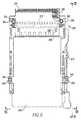
- a memory card connector 1 according to the present invention comprises a header 10 and a carrier 12 connected to the header 10.
- the connection between the header 10 and the carrier 12 can be fixed or separated in the known manner, which is not the characteristic feature of the invention and is omitted in the description hereinafter.
- the header 10 is provided with a plurality of pins 101 extended in both inward and outward directions.
- the inward pins 101 extending from the inward edge 102 of the header are used for inserting a memory card (not shown) to be received in the carrier 12.
- a vertical circuit board 14 is electrically and securely connected to the outward pins 103 extending from the outward edge 104 of the header 10.
- a connector 3 is securely mounted to the surface of a mainboard 2 for mounting the memory card connector 1.
- the lower end of the vertical circuit board 14 is detachably inserted into the connector 3 to effect electrical connection.
- the lower end of the circuit board 14 is directly plugged to the connector 3 and the bottom of connector 1 is horizontally supported by four studs 21 provided on the mainboard 2.
- the connector 1 can be fastened to the studs 21 by using screws (not shown) respectively received in the four studs 21 passing through four screw mounting holes 120 of connector 1.
- the height of the circuit board 14 is set according to the requirement of a specific application of the memory card connector so that the space between the memory card connector 1 and the mainboard 2 can be property utilized.
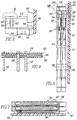
- FIG. 3 two memory card connectors 1 and 1' are stacked together and installed on the mainboard 2.
- the outward pins 103' of the upper connector 1' are longer than the outward pins 103 of the lower connector 1.
- Circuit board 14' in the upper connector 1' is larger to fit the real height as required.
- Two vertical circuit boards 14' and 14 respectively connected to the upper and lower connectors 1' and 1 are detachably and vertically connected to two corresponding connectors 3' and 3 of the mainboard 2 separately.
- a conventional memory connector 4 installed on a mainboard 5 is illustrated.
- the connector 4 comprises a plurality of bending pins 41 which are directly soldered to the mainboard 5 by using SMT.
- SMT serial to metal bus
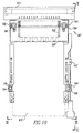
- a composite of stacked memory card connectors 201 and 201' according to another embodiment of the present invention comprises headers 210' and 210 and carriers 212' and 212 connected respectively to the headers 210' and 210. Similar to the embodiment shown in Fig. 3, two memory card connectors 201 and 201' are stacked together and installed on a mainboard 202. As with the first two embodiments, the connection between the header and the carrier can be fixed or separated in the known manner, which is not the characteristic feature of the invention and is omitted in the description hereinafter.
- the header is provided with a plurality of pins extending in both directions as in an inward direction 328' and in an outward direction as at 330' and 332' and 330 and 332.
- the inward pins extending from the inward edge of the header are used for inserting memory cards shown as at 216' in phantom lines in Fig. 5 to be received in the carrier.
- Vertical circuit boards 214' and 214 are electrically and securely connected to the outward pins extending from the outward edge of the header.
- Connectors 203' and 203 are securely mounted to the surface of a mainboard for mounting the memory card connector.
- a suitable connector would be one of the CONAN series receptacles available from Berg Electronics, Inc. of St. Louis, Missouri.
- ground plane connection between the vertical circuit board and the connector will preferably be generally equally distributed over the connector length.
- the lower end of the vertical circuit board is detachably inserted into the connector to effect electrical connection.
- the lower end of the circuit board 214' is directly plugged to the connector 203' and the lower end of circuit board 214 is directly plugged into the connector 203.
- the bottom of connector 201 and 201' are horizontally supported by four studs 333, 334, 336 and 338 provided on the mainboard.
- the connector can be fastened to the studs by using screws 340, 342, 344 and 346 respectively received in the four studs passing through four screw mounting holes as at 320 of the connector.
- the height of the circuit board 214' is set according to the requirement of a specific application of the memory card connector so that the space between the memory card connector and the mainboard can be properly utilized. It will also be seen that lower and upper memory card connectors 201 and 201' are stacked together to be installed over the mainboard.
- the outward upper pins as at 203' of the upper connector 201' are connected to the vertical board 214'.
- a conductive ground shield 322' overlaps the pins as at 330' and 332' extending from connector 201'.
- Another conductive ground shield 322 overlaps the pins as at 330 and 332 and separates those lower pins from the upper pins as at 330' and 332'.
- the vertical circuit board 214' has a central metallic ground plane 350' and opposed lateral metallic signal planes 352' and 354' which are parallel to and spaced from ground plane 350' at equal distances. These ground and signal planes extend downwardly to connector 203' to effect grounding and connection respectively to the mainboard. It will also be observed that the conductive shield 322' is isolated from signal planes 352' and 354' and contacts ground plane 350' to be grounded through that ground plane and connector 203' to the mainboard.
- pin 330' is isolated from ground plane 350' and signal plane 354' to contact signal plane 352' and to be connected through that signal plane 352' and connector 203' to the mainboard.
- Pin 332' is also isolated from ground plane 350' and signal plane 352' to contact signal plane 354' to be connected through that signal plane 354' and connector 203' to the mainboard. It will also be understood that the other outwardly extending pins which are horizontally aligned with pin 330' will contact and be connected to the mainboard through signal plane 352' and the other outwardly extending pins which are horizontally aligned with pin 332' will contact and be connected to the mainboard through signal plane 354'.
- a vertical board 214 which is connected to connector 203.
- This vertical board has an internal medial ground plane (not shown) and opposed signal planes (not shown) which are parallel to and equal distanced from the ground plane and which are essentially similar to the ones described above in connection with board 214'.
- shield 322 and pins 330 and 322 are each connected to one of said separate parallel signal planes for impedance controlled grounding and signal transmission to the mainboard.
- the use of a medial ground plane with such equally spaced parallel lateral signal planes generally allows sufficient impedance control so that various heights of the vertical boards can be used without adversely affecting performance.
- Both shields 322 and 322' shields are connected to an adjacent memory card by means of fingers as at 326 and 326'. This connection is preferably in accordance with the PCMCIA/JEIDA PC standard released February, 1995 (Document No. 0295-03-1500).
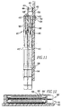
- FIG. 10-12 another composite of stacked memory card connectors 401 and 401' is shown.
- carriers 412 and 412' are connected respectively to headers 410 and 410'.
- Memory card connectors 401 and 401' are stacked together and installed on a mainboard 402.
- the connection between the header and the carrier can be fixed or separated in the known manner.
- the header is provided with a plurality of pins extending in both inward and outward directions. The inward pins extending from the inward edge of the header are used for inserting memory cards as at shown in Figure 10 in phantom lines at 416' to be received in the carrier.
- a horizontal circuit board 414 is electrically and securely connected to outward pins as at 530' and 530 extending respectively from the outward edges of both headers 410' and 410.
- a plug 404 is securely mounted to the surface of a mainboard 402 for mounting the memory card connector.
- the bottom side of the horizontal circuit board is soldered to a receptacle 403 which is engaged with plug 404 to effect electrical connection between board 414 and the mainboard.
- the bottom of connectors 401 and 401' are horizontally supported by four studs 533, 534, 536 and 538 provided on the mainboard.
- the connectors can be fastened to the studs by using screws 540, 542, 544 and 536 respectively received in the four studs passing through four screw mounting holes as at 520 of the connector.
- the horizontal circuit board 414 may be constructed similar to the vertical circuit board 214' described above with a medial ground plane interposed between parallel, equally spaced signal planes. It will also be seen that lower and upper memory card connectors 401 and 401' are stacked together to be installed over the mainboard. The outward upper pins as at 530' of the upper connector 401' extends diagonally downwardly to engage the horizontal board 414. Lower pins as at 530 from the lower board 401 extend diagonally upwardly to engage the horizontal circuit board.
- a conductive ground shield 522' overlaps the pins as at 530' extending from connector 401'.
- Another conductive ground shield 522 overlaps the pins as at 530 and separates those lower pins from the upper pins as at 530'.
- the upper and lower pins contact conductive pads respectively on the top and bottom surfaces of the horizontal circuit board and then to the signal planes.
- the shields contact conductive pads on the top and bottom surfaces of the horizontal circuit board and are then connected to the medial ground plane in the horizontal circuit board.
- Both shields 522' and 522 are connected to an adjacent memory card by means of fingers as at 526 and 526'. This connection is preferably in accordance with the PCMCIA/JEIDA PC standard released February, 1995 (Document No. 0295-03-1500).
Description
Claims (22)
- A memory card connector (201, 201'; 401, 401') for connecting a memory card (216'; 416') to a main circuit board (2; 202; 402) comprising:a. a header (210, 210'; 410, 410') having a plurality of inwardly extending pins (328'; 528') and a plurality of outwardly extending pins (230'; 330; 330', 332'; 530, 530'); andb. conductive shielding means (322, 322'; 522, 522') electrically connectable to said main circuit board (2; 202; 402) for grounding and at least partially enclosing said outwardly extending pins (103; 230'; 330; 330', 332'; 530, 530'); characterized by further comprisingc. an electric circuit board (214, 214'; 414) connectable to said outwardly extending pins (230'; 330', 332'; 330, 530, 530') and to said main circuit board (202; 402) havingc1. a conductive ground plane (350') to effect grounding of said memory card connector (201, 201'; 401, 401') to said main circuit board (202; 402), andc2. at least one separate conductive signal plane (352', 354') connected to at least some of said outwardly extending pins (330', 332') to effect electrical connection to said main circuit board (202; 402).
- The memory card connector (1, 1'; 201, 201'; 401, 401') of claim 1, characterized in that said conductive shielding means (322, 322'; 522, 522') can be grounded using said conductive ground plane (350').
- The memory card connector (1, 1'; 201, 201'; 401, 401') of claim 1, characterized in that said header (10; 210', 210; 410, 410') has an inward edge (102) and said inwardly extending pins (101'; 328'; 528') extend from said inward edge (102) of said header (10; 210, 210'; 410, 410').
- The memory card connector (1, 1'; 201, 201'; 401, 401') of claim 3, characterized in that said header (10; 210, 210'; 410, 410') has an outward edge (104) and said outwardly extending pins (103; 230'; 330', 332'; 330, 530, 530') extend from said outward edge (104) of said header (10; 210, 210'; 410, 410').
- The memory card connector (1, 1'; 201, 201'; 401, 401') of claim 2, characterized in that said electric circuit board (14, 14'; 214, 214'; 414) comprises two separate conductive signal planes (352'; 354') positioned at equal distances from said ground plane (350').
- The memory card connector (1, 1'; 201, 201'; 401, 401') of claim 5 characterized in that a first group of said outwardly extending pins (330') is connected to one signal plane (352') and a second group of said outwardly extending pins (332') is connected to said other signal plane (354').
- The memory card connector (1, 1'; 201, 201'; 401, 401') of claim 6, characterized in that said ground plane (350') is interposed in parallel spaced relation between said signal planes (352', 354').
- The memory card connector (1, 1'; 201, 201') of claim 1 characterized in that said circuit board (14, 14'; 214, 214') is positioned in generally perpendicular relation to said outwardly extending pins (103; 230'; 330', 332'; 330).
- The memory card connector (1, 1'; 201, 201') of claim 8, characterized in that said circuit board (14, 14'; 214, 214') is positioned in generally perpendicular relation to said main circuit board (2; 202).
- The memory card connector (1, 1'; 201, 201') of claim 9, characterized by further comprising a connector (3, 3'; 203; 203') on said main circuit board (2; 202) wherein a lower end of said circuit board (214; 214') is detachably inserted into said connector (203; 203').
- The memory card connector (1, 1'; 201, 201') of claim 10, characterized in that a second memory card connector (1'; 201') is positioned in spaced parallel relation to said first memory card connector (1; 201).
- The memory card connector (1, 1'; 201, 201') of claim 11, characterized in that said second memory card connector (1'; 201') comprises (a) a header (210') having a plurality of inwardly extending pins (328') and a plurality of outwardly extending pins (330', 332'); and (b) an electric circuit board (14'; 214') connected to said outwardly extending pins (103', 330', 332').
- The memory card connector (1, 1'; 201, 201') of claim 12, characterized in that at least a part of said shielding means (322) is interposed in parallel relation between said first (1; 201) and said second memory card connector (1'; 201').
- The memory card connector (1, 1'; 201, 201') of claim 11 characterized in that at least a part of said shielding means (322') is superimposed over said first (1; 201) and said second memory card connector (1', 201').
- The memory card connector (401, 401') of claim 1, characterized in that said circuit board (414) is positioned in generally parallel relation to said main circuit board (402).
- The memory card connector (401, 401') of claim 15, characterized in that said outwardly extending pins (530, 530') are oriented diagonally with respect to said circuit board (414).
- The memory card connector (401, 401') of claim 16, characterized in that said circuit board (414) is connected to said main circuit board (402) by an electrical connector (403, 404) extending perpendicularly between said circuit board (414) and main circuit board (402).
- The memory card connector (401, 401') of claim 15, characterized in that a second memory card connector (401') is positioned in spaced parallel relation to said first memory card connector (401).
- The memory card connector (401, 401') of claim 18, characterized in that said second memory card connector (401') comprises (a) a header (410') having a plurality of inwardly extending pins (528') and a plurality of outwardly extending pins (530'), and (b) an electric circuit board (414) connected to said outwardly extending pins (530').
- The memory card connector (401, 401') of claim 19, characterized in that at least a part of said shielding means (522) is interposed in parallel relation between said first (401) and said second memory card connector (401').
- The memory card connector (401, 401') of claim 20, characterized in that at least a part of said shielding means (522') is superimposed over said first (401) and said second memory card connector (401').
- A memory card connector (1, 1'; 201, 201'; 401, 401') of claim 1, characterized in that said memory card connector (1, 1'; 201, 201'; 401, 401') is connected to said main circuit board (2; 202; 402).
Applications Claiming Priority (5)
| Application Number | Priority Date | Filing Date | Title |
|---|---|---|---|
| US36961495A | 1995-01-06 | 1995-01-06 | |
| US369614 | 1995-01-06 | ||
| US48792295A | 1995-07-11 | 1995-07-11 | |
| US487922 | 1995-07-11 | ||
| PCT/US1996/000257 WO1996021257A1 (en) | 1995-01-06 | 1996-01-11 | Shielded memory card connector |
Publications (3)
| Publication Number | Publication Date |
|---|---|
| EP0801823A1 EP0801823A1 (en) | 1997-10-22 |
| EP0801823A4 EP0801823A4 (en) | 1998-03-18 |
| EP0801823B1 true EP0801823B1 (en) | 2003-05-02 |
Family
ID=27004648
Family Applications (1)
| Application Number | Title | Priority Date | Filing Date |
|---|---|---|---|
| EP96902625A Expired - Lifetime EP0801823B1 (en) | 1995-01-06 | 1996-01-11 | Shielded memory card connector |
Country Status (7)
| Country | Link |
|---|---|
| US (1) | US5711679A (en) |
| EP (1) | EP0801823B1 (en) |
| JP (1) | JP3553964B2 (en) |
| KR (1) | KR100392581B1 (en) |
| CN (1) | CN1068711C (en) |
| DE (1) | DE69627818T2 (en) |
| WO (1) | WO1996021257A1 (en) |
Families Citing this family (17)
| Publication number | Priority date | Publication date | Assignee | Title |
|---|---|---|---|---|
| JP2872618B2 (en) * | 1995-07-05 | 1999-03-17 | ヒロセ電機株式会社 | PC card connector |
| AU3961597A (en) * | 1996-07-22 | 1998-02-10 | Whitaker Corporation, The | Assembly of connector and printed circuit board |
| JP3301924B2 (en) * | 1996-10-17 | 2002-07-15 | アルプス電気株式会社 | PC card connector |
| JPH11119861A (en) * | 1997-10-09 | 1999-04-30 | Molex Inc | Connector device for card with eject mechanism |
| TW361737U (en) * | 1997-11-24 | 1999-06-11 | Hon Hai Prec Ind Co Ltd | Power connector assembly |
| US6357023B1 (en) | 1998-04-08 | 2002-03-12 | Kingston Technology Co. | Connector assembly for testing memory modules from the solder-side of a PC motherboard with forced hot air |
| US6027365A (en) * | 1998-05-28 | 2000-02-22 | The Whitaker Corporation | Test card receptacle and header |
| MY123239A (en) * | 1998-12-18 | 2006-05-31 | Molex Inc | Card-receiving connector with grounding terminal |
| JP3391721B2 (en) * | 1998-12-25 | 2003-03-31 | タイコエレクトロニクスアンプ株式会社 | Circuit board for card connector |
| TW395578U (en) * | 1998-12-31 | 2000-06-21 | Hon Hai Prec Ind Co Ltd | Electronic card connector |
| CN100452556C (en) * | 2002-01-15 | 2009-01-14 | 翠伯泰克有限公司 | Woven multiple-contact connector |
| TWM261893U (en) * | 2004-08-27 | 2005-04-11 | Molex Taiwan Ltd | Electrical connector |
| DE102006008015B3 (en) * | 2006-02-21 | 2007-04-12 | Harting Electronics Gmbh & Co. Kg | Circuit board plug set and group has plastic body by the board having two contact groups with contacts to the board on the same side of the body and plug ends on mutually opposite sides |
| US7581967B2 (en) * | 2006-08-16 | 2009-09-01 | Sandisk Corporation | Connector with ESD protection |
| CN101546875B (en) * | 2008-03-25 | 2012-06-20 | 富士康(昆山)电脑接插件有限公司 | Electronic card connector module |
| GB201205123D0 (en) * | 2012-03-23 | 2012-05-09 | Pace Plc | Mounting system for electronic components and housing therefor |
| CN106159521A (en) * | 2015-03-24 | 2016-11-23 | 鸿富锦精密工业(武汉)有限公司 | Storage device connection system, adapter and data wire |
Citations (1)
| Publication number | Priority date | Publication date | Assignee | Title |
|---|---|---|---|---|
| US5288247A (en) * | 1992-08-10 | 1994-02-22 | The Whitaker Corporation | Grounding shroud for an electrical connector |
Family Cites Families (39)
| Publication number | Priority date | Publication date | Assignee | Title |
|---|---|---|---|---|
| SE347103B (en) * | 1964-10-30 | 1972-07-24 | Olivetti & Co Spa | |
| FR1604177A (en) * | 1968-12-27 | 1971-07-26 | ||
| FR2114169A6 (en) * | 1970-11-18 | 1972-06-30 | Honeywell Bull | |
| US3676746A (en) * | 1970-12-23 | 1972-07-11 | Honeywell Inf Systems | Compatible modular circuit board connector |
| US3871728A (en) * | 1973-11-30 | 1975-03-18 | Itt | Matched impedance printed circuit board connector |
| US4600256A (en) * | 1984-12-31 | 1986-07-15 | Motorola, Inc. | Condensed profile electrical connector |
| US4858070A (en) * | 1987-04-24 | 1989-08-15 | Racal Data Communications Inc. | Modular expandable housing arrangement for electronic apparatus |
| US4755911A (en) * | 1987-04-28 | 1988-07-05 | Junkosha Co., Ltd. | Multilayer printed circuit board |
| JPH0633656Y2 (en) * | 1987-12-21 | 1994-08-31 | 株式会社村田製作所 | Surface mount type connector |
| US5113317A (en) * | 1990-02-20 | 1992-05-12 | Allen-Bradley Company, Inc. | Support for auxiliary circuit card |
| US4997377A (en) * | 1990-02-22 | 1991-03-05 | Amp Incorporated | Adaptor for computers |
| US5151033A (en) * | 1990-09-13 | 1992-09-29 | Hirose Electric Co., Ltd. | Electrical connector |
| US5085590A (en) * | 1990-10-30 | 1992-02-04 | Amp Incorporated | Shielded stackable connector assembly |
| US5224019A (en) * | 1991-03-15 | 1993-06-29 | Amkly Systems, Inc. | Modular computer assembly |
| US5201662A (en) * | 1991-08-23 | 1993-04-13 | Molex Incorporated | Electrical connector for mounting on a printed circuit board |
| JP2659030B2 (en) * | 1991-09-12 | 1997-09-30 | デュポン・シンガポール・ピーティーイー・リミテッド | Connector device |
| US5299089A (en) * | 1991-10-28 | 1994-03-29 | E. I. Dupont De Nemours & Co. | Connector device having two storage decks and three contact arrays for one hard disk drive package or two memory cards |
| US5194010A (en) * | 1992-01-22 | 1993-03-16 | Molex Incorporated | Surface mount electrical connector assembly |
| US5224865A (en) * | 1992-02-24 | 1993-07-06 | Hughes Aircraft Company | Sliding wedge electrical connector |
| US5225968A (en) * | 1992-03-10 | 1993-07-06 | Ma Hsi K | Connecting apparatus for connecting computer functional cards to a mother board |
| US5161999A (en) * | 1992-03-18 | 1992-11-10 | Amp Incorporated | Surface mount electrical cohnnector and shield therefor |
| US5260854A (en) * | 1992-05-14 | 1993-11-09 | Sun Microsystems, Inc. | Modular circuit board placement system |
| US5259783A (en) * | 1992-05-15 | 1993-11-09 | Sun Microsystems, Inc. | Dual height card retainer |
| US5318452A (en) * | 1992-08-10 | 1994-06-07 | The Whitaker Corporation | Electrical connector |
| US5297966A (en) * | 1992-08-10 | 1994-03-29 | The Whitaker Corporation | Mounting bracket for an electrical connector |
| US5290174A (en) * | 1992-08-10 | 1994-03-01 | The Whitaker Corporation | Electrical connector for a card reader |
| US5268820A (en) * | 1992-08-18 | 1993-12-07 | Mitac International Corp. | Mother board assembly |
| US5277615A (en) * | 1992-09-24 | 1994-01-11 | Compaq Computer Corporation | Apparatus for removably supporting a plurality of hot plug-connected hard disk drives |
| US5305182A (en) * | 1992-10-14 | 1994-04-19 | Chen Teng Ka | Read/write unit for two integrated circuit cards |
| US5415569A (en) * | 1992-10-19 | 1995-05-16 | Molex Incorporated | Filtered electrical connector assembly |
| US5408386A (en) * | 1992-10-30 | 1995-04-18 | Intel Corporation | Socket assembly including a first circuit board located between a receptacle housing and a second circuit board |
| US5286207A (en) * | 1992-12-21 | 1994-02-15 | Foxconn International, Inc. | Memory card connector |
| JP2603509Y2 (en) * | 1992-12-28 | 2000-03-15 | 日本エー・エム・ピー株式会社 | Card edge connector |
| US5334046A (en) * | 1993-02-22 | 1994-08-02 | Augat Inc. | Circuit card interface system |
| JP2567629Y2 (en) * | 1993-03-23 | 1998-04-02 | バーグ・テクノロジー・インコーポレーテッド | Connector device |
| US5316488A (en) * | 1993-06-04 | 1994-05-31 | Molex Incorporated | Connector apparatus for IC packs |
| US5267876A (en) * | 1993-06-16 | 1993-12-07 | The Whitaker Corporation | Board saving stacked electrical connector assembly |
| US5399105A (en) * | 1994-04-29 | 1995-03-21 | The Whitaker Corporation | Conductive shroud for electrical connectors |
| US5478260A (en) * | 1994-07-29 | 1995-12-26 | The Whitaker Corporation | Grounding for electrical connectors |
-
1996
- 1996-01-11 WO PCT/US1996/000257 patent/WO1996021257A1/en active IP Right Grant
- 1996-01-11 CN CN96191370A patent/CN1068711C/en not_active Expired - Lifetime
- 1996-01-11 JP JP52125896A patent/JP3553964B2/en not_active Expired - Fee Related
- 1996-01-11 EP EP96902625A patent/EP0801823B1/en not_active Expired - Lifetime
- 1996-01-11 DE DE69627818T patent/DE69627818T2/en not_active Expired - Lifetime
- 1996-11-20 US US08/752,756 patent/US5711679A/en not_active Expired - Lifetime
-
1997
- 1997-07-05 KR KR10-1997-0704628A patent/KR100392581B1/en not_active IP Right Cessation
Patent Citations (1)
| Publication number | Priority date | Publication date | Assignee | Title |
|---|---|---|---|---|
| US5288247A (en) * | 1992-08-10 | 1994-02-22 | The Whitaker Corporation | Grounding shroud for an electrical connector |
Also Published As
| Publication number | Publication date |
|---|---|
| EP0801823A1 (en) | 1997-10-22 |
| EP0801823A4 (en) | 1998-03-18 |
| CN1068711C (en) | 2001-07-18 |
| CN1168199A (en) | 1997-12-17 |
| KR19980701239A (en) | 1998-05-15 |
| DE69627818D1 (en) | 2003-06-05 |
| JP3553964B2 (en) | 2004-08-11 |
| KR100392581B1 (en) | 2003-08-19 |
| DE69627818T2 (en) | 2004-04-08 |
| WO1996021257A1 (en) | 1996-07-11 |
| US5711679A (en) | 1998-01-27 |
| JP2001508915A (en) | 2001-07-03 |
Similar Documents
| Publication | Publication Date | Title |
|---|---|---|
| EP0801823B1 (en) | Shielded memory card connector | |
| EP0578888B1 (en) | Data card perimeter shield | |
| EP0935912B1 (en) | Pcmcia card with metal cover, connector, frame with cross beam and exposed ground plate disposed on connector | |
| US5713747A (en) | Memory card connector | |
| US5688130A (en) | Electrical connector assembly for pc cards | |
| KR100307308B1 (en) | Shielded PC Card Holder | |
| US6183292B1 (en) | Shielded modular jack | |
| EP0682322B1 (en) | An IC card | |
| EP0740373B9 (en) | High performance card edge connector | |
| US6932626B2 (en) | Electrical card connector | |
| US20030220020A1 (en) | High speed connector with matched impedance | |
| US6091605A (en) | Memory card connector and cover apparatus and method | |
| JPH10506222A (en) | Improved ground shroud for electrical connectors | |
| US5807137A (en) | Shielded electrical receptacle connector assembly | |
| US7014506B2 (en) | Board mounted memory card connector | |
| JP2004146271A (en) | Multiple step type electric connector | |
| JPH11317259A (en) | Boxy shield of modular structure | |
| US6634905B2 (en) | Stacked electrical card connector assembly | |
| US6322392B1 (en) | Ground plate structure for a PC card connector assembly | |
| US6551132B1 (en) | Stacked electrical card connector assembly | |
| US5584706A (en) | IC card connector having two grounding contacts | |
| CN2596577Y (en) | Electronic card connector |
Legal Events
| Date | Code | Title | Description |
|---|---|---|---|
| PUAI | Public reference made under article 153(3) epc to a published international application that has entered the european phase |
Free format text: ORIGINAL CODE: 0009012 |
|
| 17P | Request for examination filed |
Effective date: 19970702 |
|
| AK | Designated contracting states |
Kind code of ref document: A1 Designated state(s): DE FR GB |
|
| RIN1 | Information on inventor provided before grant (corrected) |
Inventor name: LU, LEIN, WAN Inventor name: AMANO, KAZUTOSHI Inventor name: SPICKLER, JOHN, M. Inventor name: HSAI, CHIH-HUI |
|
| A4 | Supplementary search report drawn up and despatched |
Effective date: 19980130 |
|
| AK | Designated contracting states |
Kind code of ref document: A4 Designated state(s): DE FR GB |
|
| RAP1 | Party data changed (applicant data changed or rights of an application transferred) |
Owner name: BERG ELECTRONICS MANUFACTURING B.V. |
|
| 17Q | First examination report despatched |
Effective date: 20000613 |
|
| GRAH | Despatch of communication of intention to grant a patent |
Free format text: ORIGINAL CODE: EPIDOS IGRA |
|
| RAP1 | Party data changed (applicant data changed or rights of an application transferred) |
Owner name: FCI |
|
| GRAH | Despatch of communication of intention to grant a patent |
Free format text: ORIGINAL CODE: EPIDOS IGRA |
|
| GRAA | (expected) grant |
Free format text: ORIGINAL CODE: 0009210 |
|
| RIC1 | Information provided on ipc code assigned before grant |
Ipc: 7H 01R 12/20 B Ipc: 7H 01R 12/18 B Ipc: 7H 01R 12/16 B Ipc: 7H 01R 12/32 B Ipc: 7H 01R 12/04 A |
|
| AK | Designated contracting states |
Designated state(s): DE FR GB |
|
| REG | Reference to a national code |
Ref country code: GB Ref legal event code: FG4D |
|
| REF | Corresponds to: |
Ref document number: 69627818 Country of ref document: DE Date of ref document: 20030605 Kind code of ref document: P |
|
| ET | Fr: translation filed | ||
| PLBE | No opposition filed within time limit |
Free format text: ORIGINAL CODE: 0009261 |
|
| STAA | Information on the status of an ep patent application or granted ep patent |
Free format text: STATUS: NO OPPOSITION FILED WITHIN TIME LIMIT |
|
| 26N | No opposition filed |
Effective date: 20040203 |
|
| PGFP | Annual fee paid to national office [announced via postgrant information from national office to epo] |
Ref country code: GB Payment date: 20101215 Year of fee payment: 16 |
|
| REG | Reference to a national code |
Ref country code: FR Ref legal event code: CA |
|
| PGFP | Annual fee paid to national office [announced via postgrant information from national office to epo] |
Ref country code: FR Payment date: 20120111 Year of fee payment: 17 |
|
| PGFP | Annual fee paid to national office [announced via postgrant information from national office to epo] |
Ref country code: DE Payment date: 20120131 Year of fee payment: 17 |
|
| REG | Reference to a national code |
Ref country code: DE Ref legal event code: R082 Ref document number: 69627818 Country of ref document: DE Representative=s name: BEETZ & PARTNER PATENT- UND RECHTSANWAELTE, DE Effective date: 20120419 Ref country code: DE Ref legal event code: R081 Ref document number: 69627818 Country of ref document: DE Owner name: FCI, FR Free format text: FORMER OWNER: FCI, PARIS, FR Effective date: 20120419 |
|
| GBPC | Gb: european patent ceased through non-payment of renewal fee |
Effective date: 20130111 |
|
| REG | Reference to a national code |
Ref country code: FR Ref legal event code: ST Effective date: 20130930 |
|
| PG25 | Lapsed in a contracting state [announced via postgrant information from national office to epo] |
Ref country code: DE Free format text: LAPSE BECAUSE OF NON-PAYMENT OF DUE FEES Effective date: 20130801 |
|
| REG | Reference to a national code |
Ref country code: DE Ref legal event code: R119 Ref document number: 69627818 Country of ref document: DE Effective date: 20130801 |
|
| PG25 | Lapsed in a contracting state [announced via postgrant information from national office to epo] |
Ref country code: GB Free format text: LAPSE BECAUSE OF NON-PAYMENT OF DUE FEES Effective date: 20130111 Ref country code: FR Free format text: LAPSE BECAUSE OF NON-PAYMENT OF DUE FEES Effective date: 20130131 |