EP0789439A1 - Device for controlling the charging voltage of a battery which is charged by an alternator depending on a reference voltage and the rotational speed of the alternator - Google Patents
Device for controlling the charging voltage of a battery which is charged by an alternator depending on a reference voltage and the rotational speed of the alternator Download PDFInfo
- Publication number
- EP0789439A1 EP0789439A1 EP97400264A EP97400264A EP0789439A1 EP 0789439 A1 EP0789439 A1 EP 0789439A1 EP 97400264 A EP97400264 A EP 97400264A EP 97400264 A EP97400264 A EP 97400264A EP 0789439 A1 EP0789439 A1 EP 0789439A1
- Authority
- EP
- European Patent Office
- Prior art keywords
- signal
- alternator
- voltage
- speed
- comparator means
- Prior art date
- Legal status (The legal status is an assumption and is not a legal conclusion. Google has not performed a legal analysis and makes no representation as to the accuracy of the status listed.)
- Withdrawn
Links
Images


Classifications
-
- H—ELECTRICITY
- H02—GENERATION; CONVERSION OR DISTRIBUTION OF ELECTRIC POWER
- H02J—CIRCUIT ARRANGEMENTS OR SYSTEMS FOR SUPPLYING OR DISTRIBUTING ELECTRIC POWER; SYSTEMS FOR STORING ELECTRIC ENERGY
- H02J7/00—Circuit arrangements for charging or depolarising batteries or for supplying loads from batteries
- H02J7/14—Circuit arrangements for charging or depolarising batteries or for supplying loads from batteries for charging batteries from dynamo-electric generators driven at varying speed, e.g. on vehicle
- H02J7/1446—Circuit arrangements for charging or depolarising batteries or for supplying loads from batteries for charging batteries from dynamo-electric generators driven at varying speed, e.g. on vehicle in response to parameters of a vehicle
-
- Y—GENERAL TAGGING OF NEW TECHNOLOGICAL DEVELOPMENTS; GENERAL TAGGING OF CROSS-SECTIONAL TECHNOLOGIES SPANNING OVER SEVERAL SECTIONS OF THE IPC; TECHNICAL SUBJECTS COVERED BY FORMER USPC CROSS-REFERENCE ART COLLECTIONS [XRACs] AND DIGESTS
- Y02—TECHNOLOGIES OR APPLICATIONS FOR MITIGATION OR ADAPTATION AGAINST CLIMATE CHANGE
- Y02T—CLIMATE CHANGE MITIGATION TECHNOLOGIES RELATED TO TRANSPORTATION
- Y02T10/00—Road transport of goods or passengers
- Y02T10/80—Technologies aiming to reduce greenhouse gasses emissions common to all road transportation technologies
- Y02T10/92—Energy efficient charging or discharging systems for batteries, ultracapacitors, supercapacitors or double-layer capacitors specially adapted for vehicles
Definitions
- the present invention relates generally to devices for regulating the charging voltage of a battery by an alternator in a motor vehicle.
- It relates more particularly to a new regulating device intended to ensure satisfactory regulation in association with combustion engines exhibiting, at low rotation speeds, significant acyclism, that is to say large variations in the rotation speed of the engine.
- the regulating device provides for controlling the excitation of the alternator no longer as a function of the current demanded by consumers, but as a function of a law of admissible reduction in the speed of rotation of the engine or of the alternator.
- the law of authorized reduction in speed (or authorized increase in period, signal VP2 in FIG. 1 of FR-A-2 691 020) is established from a value of actual period taken on the fly from an alternator phase signal. This value of real period varying in large proportions due to acyclism, it is very likely that the aforementioned law will present an incorrect starting point, namely either a period too low, or a period too high.
- the present invention aims to overcome these drawbacks of the known technique, and to propose a new regulation device which overcomes the problems associated with acyclism at idle of the associated combustion engine.
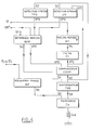
- FIG. 1 there is shown a block diagram of a circuit for regulating the charging voltage of a battery by an alternator according to the invention.
- It includes a block M1 intended to measure the instantaneous period of rotation of the alternator, on the basis of a signal ⁇ obtained itself from phase signals taken from the stator windings of the alternator.
- This block delivers an analog signal P1 representative of the value of this period.
- the signal ⁇ is preferably not a simple potential difference taken directly from the stator windings of the alternator, but consists of a clean rectangular signal whose period is proportional to the rotation period of l 'alternator.
- An embodiment of a circuit capable of developing the signal ⁇ as a function of phase potentials ⁇ 1 and ⁇ 2 taken from the stator windings will be described later.
- the signal P1 is applied to the input of a block F1 which has the role of filtering the signal P1 to obtain an average value of the period of rotation, denoted VP1.
- the circuit also includes a block designated by RFP, which has the purpose of generating a period reference signal, noted VP2.
- This signal is produced as a function of the value of the battery voltage UB + taken on the output of the alternator or on the battery itself, relative to a fixed reference voltage, and this within a determined operating range.
- this RFP block receives on an input a signal S1 constituting said reference voltage, to which the voltage UB + or a predetermined fraction of this voltage obtained using a resistive divider bridge is compared.
- the block COMP constitutes an analog comparator which receives on a first comparison input the signal of average period VP1 and on a second comparison input the reference signal of period VP2, and which outputs a logic signal S2 from which, as we will see, the alternator excitation control signal will be developed.
- the filtering carried out by the block F1 advantageously has a filtering rate such that its output signal VP1 retains a substantial alternative component, while the signal VP2 evolves much slower, practically without any alternative component.
- the comparison between the signals VP1 and VP2 makes it possible to provide an output signal S2 chopped at a relatively high frequency, in synchronism with the phase signal delivered by the alternator.
- the frequency of the signal S2 is typically 1500 Hz. This value may prove to be too large and cause in the organ of power switching of the excitation winding of significant switching losses.
- a circuit TP1 which constitutes a time delay intended to extend the duration of the signal S2 in such a situation, in order to limit the switching losses.
- the frequency of the excitation signal is limited to a value of 500 Hz, which is entirely acceptable.
- the output signal S3 of the circuit TP1 is applied to the input of a power stage (block EX) which supplies the excitation winding IND of the alternator, for example from the battery voltage.
- the circuit of FIG. 1 further comprises a phase regulation block, denoted RP, intended to cause a priority increase in the excitation when the amplitude of a phase signal ⁇ 1 or ⁇ 2 taken on a stator winding of the the alternator becomes less than a predetermined limit, in order to increase this amplitude.
- RP phase regulation block
- VP2 tends to converge towards VP1 and, when the two values are close to each other, the device behaves practically like a conventional voltage regulator.
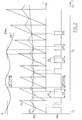
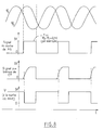
- This operating phase is illustrated between times t1 and t2 in FIG. 2.
- the signal VP1 can, through the play of a limited filtering rate, present a significant residual alternative component, as illustrated in FIG. 2.
- the signal d is split up. excitation S2 applied to the input of the block TP1, with in this signal rising or falling edges each time that the signal VP1 crosses the signal VP2 down and up, respectively. This does not prevent, as we saw above, to see the value of VP2 converge towards the average value of VP1.
- the average value of the period signal VP1 decreases faster than the reference signal VP2.
- the comparison made between VP1 and VP2 when UB + is less than Ureg therefore tends to increase the excitation of the alternator, since the durations during which VP1 is located below VP2 become longer.
- the authorized drop in speed without limiting the alternator flow rate is determined by the growth slope of the signal VP2.
- the drop in speed is caused by the commissioning in the on-board network of a load consuming a large amount of current, the supply of the loads will remain correct if this drop in speed does not exceed the value imposed by the slope of VP2.
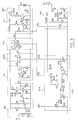
- the period measurement block M1 is constructed around the transistor stages T1, T2, T3 and T4.
- the capacitor C2 is charged by a constant current source constituted by T3 and R7, then suddenly discharged by T4 each time this transistor is passed through a positive edge of the phase signal transmitted via T1, T2 and C1.
- the filtering function performed by the block F1 is constructed around the operational amplifier A1, the charge of the capacitor C3 depending on the comparison between the output signal VP1 and the input signal P1 performed by said operational amplifier.
- a filtered signal VP1 is therefore obtained at the output, but retaining, by an appropriate choice of the values of C3 and the associated resistances, an alternative component as illustrated in FIG. 2.
- the COMP block consists of a simple operational amplifier A2 mounted as a comparator and outputting the signal S2.
- the function TP1 is an ordinary time delay carried out for example by a logic counter circuit CL1 controlled by a clock CK, to form the signal S3.
- the power circuit for excitation control (block EX) is of conventional design, with a power transistor T8 in this case bipolar.
- the freewheeling diode associated with the excitation winding IND consists of D4.
- the circuit corresponding to the RFP block includes a resistive divider bridge R18, R19 receiving the voltage UB +.
- the components R20 and C4 provide filtering before the divided signal is compared to an external voltage reference S1 at the level of an operational amplifier A3 mounted as a comparator.
- the signal S4 is obtained at the output of the stage built around T4 and receiving the output signal from A3.
- the period reference signal VP2 is obtained by charging and discharging the capacitor C5, the charging taking place via R26 and R25 when T10 is blocked and the discharging taking place via R25 and T10 when T10 is on, this transistor T10 being driven by the output of comparator A3.
- the priority character of the signal S4 at the input of the timer circuit TP1 to suppress the excitation is achieved by using said signal S4 as reset signal of the timer CL1, which, after the timer duration (for example 2 ms as indicated above), blocks the excitation.
- the RP block includes a diode D5 and a capacitor C6 which memorize the peak value of the phase signal ⁇ 1 or ⁇ 2 applied at the input. In normal operation, this stored value is greater than the threshold voltage of the zener diode DZ1, which then leads in reverse. The transistor T11 is therefore conducting, while T12 is blocked. There is therefore no influence on the operation of the regulation, because the signal S5 is in high impedance. On the other hand, if the phase signal ⁇ 1 or ⁇ 2 sees its amplitude decreasing excessively, the value memorized in the capacitor C6 becomes lower than the threshold voltage of DZ1, which blocks T11 and makes T12 conductive. The signal S5 then takes a value close to 0 volts, which forces the excitation to be restored via the EX block whatever the state of its control signal S3.
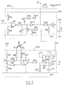
- FIGS. 4 and 5 there is shown, in the form of a block diagram and in the form of an analog circuit diagram, an alternative embodiment of the device of FIGS. 1 and 3, which is remarkable in that it comprises in in addition to a peak detection device, designated by TP2, and a speed detection device, denoted DV.
- TP2 peak detection device
- DV speed detection device
- the purpose of the TP2 block is to deal with the particular situation in which the alternator is in "full field", that is to say that following a large current demand, the excitation is carried out continuously for a substantial period.
- the values of VP1 and of VP2 diverge, since the voltage UB + being lower than Ureg for an extended period, VP2 increases during this entire period.
- the signal VP2 after having crossed the signal VP1 upwards, leaves in abutment on a positive limit constituted by the supply voltage Vcc of the circuits (typically 5 volts) or a voltage close to the latter.
- the purpose of the circuit TP2 is to limit the growth of the signal VP2 during the full field regime to an upper limit lower than that determined by the supply voltage of the circuits, and in l 'species at a value equal to the peak value of the signal VP1.
- the block TP2 comprises a time delay, for example of a value of 240 ms and constituted by a logic counter circuit CL2 clocked by the clock CK and whose reset input is controlled by a logic inverter INV1 receiving the signal S2 as an input.
- a time delay TP2 is reset to zero, so that the transistor T14 remains blocked.
- the TP2 block therefore has no influence on the VP2 signal, which continues to grow.
- the DV block constitutes a speed detector whose object is to limit the operating range of the regulation by the signals VP1 and VP2 to a given range of rotation speeds of the alternator.
- This regulation based on the period is indeed of great interest mainly in the case of a rotation of the heat engine at idle, in order to stabilize this idle speed in the event that large current demands appear on the vehicle's on-board network. , which corresponds for example to an upper limit of 2000 revolutions / minute at the alternator.
- the speed detector DV comprises an operational amplifier A4 mounted as a comparator, which compares the value of the signal VP1 with a threshold voltage S5 'established by a resistive divider bridge R31, R32.
- the output of comparator A4 drives an input e1 of a NOR logic gate designated by NOR1, the other input e2 of which selectively receives, using a switch IC, either the signal S2 or a zero voltage ( mass).
- the output of this gate controls a transistor T13 developing a signal VP3 applied to the RFP block.
- the input e2 of the gate NOR1 can also, using the switch IC, receive the signal S2.
- the resistor R33 causes, by means of the load of C5, the signal VP2 beyond the peak value of VP1.
- T13 is blocked and the rapid charging of C5 via the resistor R33 is interrupted.
- the switch IC can be controlled according to an appropriate logic so that the block DV can take the place of both a speed detection circuit and a peak detection circuit for speeds in this case greater than 2500 rpm.
- the timer circuit TP1 remains useful in a normal regulation mode to avoid erratic regulation taking place on the residual AC component of the rectified output voltage of the alternator.
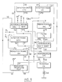
- FIG. 6 shows, in the form of a block diagram, another alternative embodiment of the invention which, compared to that of FIGS. 4 and 5, is enriched with two new functions constituted by the DVA and DPH blocks.
- An example of electronic construction of these blocks is illustrated in FIG. 7.
- the purpose of the DPH block is to detect the start of the alternator rotation by measuring the difference in electromotive force (fem) noted between two windings of the stator ST of the alternator, whose potentials are noted ⁇ 1 and ⁇ 2 , respectively.
- the threshold for this detection corresponds to a difference of about 0.2 V between the aforementioned potentials.
- Its output signal, noted S6, attacks an input of the DVA block.
- the latter which is preferably integrated into the COMP block, fulfills a function of detecting the priming speed of the alternator, for example around 1200 rpm. To this end, it receives on an input the signal VP1, which is compared with a set value.
- the purpose of the DVA circuit is to maintain the capacitor C5 of the RFP circuit, by acting on the signal line VP2, in the discharged state until the alternator has reached its aforementioned ignition rotation speed. .
- the S7 output of the DVA block attacks an input of the regulation block on the RP phase, for purposes explained below.
- the DPH block comprises an operational amplifier A5 mounted as a comparator, with a set of associated resistances R39 to R42, this comparator receiving the winding potentials ⁇ 1 and ⁇ 2 on its two respective inputs.
- the diode D7 connected in series with two resistors R37 and R38 between the voltage UB + and the ground is intended to fix, by its direct junction voltage, the detection threshold of the potential difference ⁇ 1 and ⁇ 2.
- this junction voltage is 0.8 volts and if the ratio between the ohmic values of R39, R40 on the one hand, and R41, R42 on the other hand, is equal to four, then we obtain a threshold of 0.2 volt detection as mentioned above.
- This comparator stage is followed by an asymmetrical filter constituted by the components R43, R44, D8 and C7.
- the purpose of this filter is, by keeping the capacity C7 discharged as soon as the frequency of the signal at the output of A5 has a high value, for example greater than 20 kHz, to avoid taking into account when detecting the high frequency components. passing through the potentials ⁇ 1 and ⁇ 2 due to radio interference (radio telephones, "Citizen Band” devices, police transmitters, port stations, etc.).
- the output of this filter attacks the reset input RESET of a time delay constituted by a logic counter CL3 controlled by the clock signal CK.
- the time delay value here is 50 ms.
- Zener DZ2 diode The purpose of the Zener DZ2 diode is to limit the voltage delivered by A5 to a value compatible with the reset input of the circuit CL3 (typically 5 volts).
- the timer CL3 delivers as an output a signal S6 which attacks, as will be seen below, an input of the DVA block, the value of the signal S6 being a logic "1" (5 volts) if the alternator is stopped, and a logical "0" (ground) as soon as the alternator starts to rotate.
- the DPH circuit is advantageously used here to construct the signal ⁇ described above, the period of which is proportional to the period of rotation of the alternator.
- a logic inverter circuit INV2 outputs the phase signal ⁇ from the signal taken from the upper terminal of C7.
- FIG. 8 shows, from top to bottom, the phase signals ⁇ 1 and ⁇ 2, the signal at the output of comparator A5, the signal at the terminals of capacitor C7 (after filtering), and finally the signal ⁇ at output of l INV2 logic inverter.
- the DVA circuit comprises an operational amplifier A6 mounted as a comparator, which compares the mean period signal VP1 with a set value fixed by the divider bridge R45, R46 connected between the DC supply voltage Vcc and the ground.
- the capacitor C8 charges as soon as said average value VP1 becomes lower than this setpoint.
- the capacitor C8 is then locked in its charged state by the circuit constituted by the logic inverters INV3 and INV4, the resistor R48 and the diode D9 as long as the alternator remains in rotation at a speed at least equal to the priming speed. . More precisely, C8 can only discharge when the signal S6 delivered by the DPH block goes to the high logic level, which makes the transistor T15 conductive, that is to say only when no rotation of the alternator is detected by the DPH block.
- the charge of C8 itself causes, by the play of the inverter INV3, the blocking of T16, which then authorizes the charge of C5 and therefore the increase in the value of the signal VP2.
- the DVA circuit therefore makes it possible to ensure a delay of the rise in excitation of the alternator, this delay extending as long as the signal VP2 is less than VP1 from the moment when the alternator has reached its ignition regime.
- the DVA detection block also includes an S7 output which is intended to avoid a permanent excitation is caused by the RP phase regulation block below the alternator priming speed, or even when the alternator is stopped.
- the signal S7 taken at the output of the inverter INV3, attacks via a resistor the base of the transistor T11 of the block RP, to block the operation of the latter under these conditions.
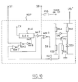
- a priority regulation block denoted RGP, is added to the regulation circuit described above, intended to maintain a minimum voltage level on the battery (for example around 9.75 volts) when such a level voltage has been exceeded at least once for a period greater than or equal to a threshold (for example 0.5 seconds) when starting the vehicle.
- RGP a priority regulation block
- This priority regulation function is intended to enter into action as soon as the DVA unit has detected a rotation of the alternator greater than its priming speed.
- This RGP circuit is shown in detail in Figure 10.
- It includes a stage for detecting the level of the battery voltage UB + constituted by the transistor T17, the resistors R53 to R56, the diode D10 and the Zener diode DZ3. It also includes a timer built around a logic counter CL4, and a logic circuit consisting of a set of gates NOR1 ', NOR2 and NOR3 (NOR gates) and INV5, IN6 and INV7 (logic inverters), this receiving circuit at an input of the NOR2 gate the signal S7 delivered by the DVA block. It is also planned
- the transistor T17 compares the battery voltage UB + to a threshold voltage constituted by the avalanche voltage of the Zener diode DZ3, and is in the blocked state when UB + is greater than said avalanche voltage, fixed at 9.75 volts for example.
- the signal S7 When the alternator speed is lower than its ignition speed (here 1200 rpm), the signal S7 is at logic level "1", which maintains via NOR2 and INV6 the reset of timer CL4 at level of its reset input. As soon as the alternator speed has crossed the threshold of 1200 rpm, the signal S7 goes to logic level "0" and the time delay can run, provided that the transistor T17 is blocked, that is to say say that a logic level "1" is applied to the corresponding input of gate NOR1 via the logic inverter INV5.
- a priority regulation signal S9 on 9.75 volts developed via INV7 and NOR3 from the timer output, is applied to the RFP block via a MEL mixing circuit represented as being incorporated therein. block.
- phase regulation (with an amplitude of for example 7.5 volts) can only be carried out when the battery voltage is maintained above 9.75 volts. Any charge of the battery is therefore avoided by the phase regulation circuit before the end of the time delay produced by the circuit CL4.
- FIG. 11 illustrates an alternative embodiment of FIG. 5
- FIG. 11 illustrates an alternative embodiment of FIG. 5
- the RFP period reference circuit is associated with a mixing circuit MEL which replaces the transistor T9 which on the Figure 5 was associated with the RFP circuit.
- This MEL circuit consists of two NOR gates designated by NOR4 and NOR5.
- phase regulation carried out in the RP block can be put into service, as desired, either directly by the priming detection circuit DVA, via the signal S7 , or by the priority regulation circuit RGP, via the signal S8.
- signal used throughout this specification may mean, depending on the case, an analog voltage, a logic value “0” or “1” or even a digital word of N bits, N being chosen in particular as a function the processing precision required.
Abstract
Description
La présente invention a trait d'une façon générale aux dispositifs régulateurs de la tension de charge d'une batterie par un alternateur dans un véhicule automobile.The present invention relates generally to devices for regulating the charging voltage of a battery by an alternator in a motor vehicle.
Elle concerne plus particulièrement un nouveau dispositif régulateur destiné à assurer une régulation satisfaisante en association avec des moteurs à combustion présentant, à des régimes de rotation faibles, un acyclisme important, c'est-à-dire de fortes variations de la vitesse de rotation du moteur.It relates more particularly to a new regulating device intended to ensure satisfactory regulation in association with combustion engines exhibiting, at low rotation speeds, significant acyclism, that is to say large variations in the rotation speed of the engine.
On connaît par FR-A-2 691 020 au nom de la Demanderesse un dispositif de régulation destiné, lors de la mise en service de consommateurs de courant important, à éviter que le couple résistant présenté au moteur thermique par l'alternateur ne vienne réduire encore un régime de rotation déjà bas et risque de faire hoqueter ou caler le moteur.We know from FR-A-2 691 020 in the name of the Applicant a regulation device intended, during the commissioning of large current consumers, to prevent the resistive torque presented to the heat engine by the alternator from reducing still an already low rotation speed and risks making the engine hiccup or stall.
A cet effet, le dispositif de régulation selon ce document prévoit de contrôler l'excitation de l'alternateur non plus en fonction du courant demandé par les consommateurs, mais en fonction d'une loi de diminution admissible de la vitesse de rotation du moteur ou de l'alternateur.To this end, the regulating device according to this document provides for controlling the excitation of the alternator no longer as a function of the current demanded by consumers, but as a function of a law of admissible reduction in the speed of rotation of the engine or of the alternator.
Cette solution s'avère tout à fait satisfaisante pour des moteurs thermiques présentant un régime de rotation au ralenti relativement stable.This solution proves to be entirely satisfactory for internal combustion engines having a relatively stable idling speed.
L'acyclisme du régime de rotation au ralenti des moteurs thermiques est cependant un phénomène que l'on rencontre de plus en plus souvent dans les moteurs thermiques modernes. Plus précisément, afin notamment de diminuer la pollution et la consommation de carburant, on tend aujourd'hui à donner aux moteurs un régime de ralenti extrêmement réduit, avec lequel les compressions et les injections de carburant successives au niveau des cylindres provoquent des variations importantes de la vitesse de rotation du moteur au ralenti, et ces variations perturbent le fonctionnement du dispositif de régulation du document précité.The acyclism of the idling speed of heat engines is, however, a phenomenon that is increasingly encountered in modern heat engines. More specifically, in order in particular to reduce pollution and fuel consumption, there is today a tendency to give the engines an extremely reduced idling speed, with which the successive compressions and injections of fuel at the cylinders cause significant variations in engine idling speed, and these variations disturb the operation of the regulation device of the above-mentioned document.
Plus précisément, dans ce dispositif de régulation connu, pour un débit donné de l'alternateur défini par les charges électriques en service, un accroissement de la vitesse de rotation provoque une diminution du rapport cyclique de la commande d'excitation, tandis qu'une diminution de la vitesse de rotation provoque au contraire un accroissement de ce rapport cyclique. Ces fortes variations de rapport cyclique peuvent en particulier amener le régulateur dans un état de fonctionnement plein champ, ce qui est détecté par le dispositif régulateur pour entrer accidentellement dans le mode de régulation en fonction de la vitesse et non plus en fonction de la tension de sortie de l'alternateur, alors qu'aucune nouvelle charge n'a été mise en service.More precisely, in this known regulation device, for a given flow rate of the alternator defined by the electrical charges in service, an increase in the speed of rotation causes a reduction in the duty cycle of the excitation control, while a decreasing the speed of rotation, on the contrary, causes an increase in this duty cycle. These large variations in duty cycle can in particular bring the regulator into a full field operating state, which is detected by the regulating device to accidentally enter the regulation mode as a function of the speed and no longer as a function of the voltage. alternator output, while no new load has been put into service.
En outre, dans le régulateur connu, la loi de diminution autorisée de la vitesse (ou d'accroissement autorisé de la période, signal VP2 sur la figure 1 de FR-A-2 691 020) est établie à partir d'une valeur de période réelle prise à la volée à partir d'un signal de phase de l'alternateur. Cette valeur de période réelle variant dans de grandes proportions du fait de l'acyclisme, il est très probable que la loi précitée présentera un point de départ incorrect, à savoir soit une période trop faible, soit une période trop élevée.In addition, in the known regulator, the law of authorized reduction in speed (or authorized increase in period, signal VP2 in FIG. 1 of FR-A-2 691 020) is established from a value of actual period taken on the fly from an alternator phase signal. This value of real period varying in large proportions due to acyclism, it is very likely that the aforementioned law will present an incorrect starting point, namely either a period too low, or a period too high.
Dans le premier cas, il en résulte une suppression de l'excitation pendant une durée prolongée, et une sous-alimentation indésirable des charges. Dans le second cas, il en résulte au contraire une reprise hâtive de l'excitation, et une diminution indésirable du régime de ralenti.In the first case, this results in a suppression of the excitation for a prolonged period, and an undesirable undernourishment of the loads. In the second case, on the contrary, this results in a hasty resumption of the excitation, and an undesirable reduction in the idling speed.
Ainsi la régulation conforme à l'antériorité ne peut fonctionner correctement en présence d'acyclisme.Thus the regulation conforming to the anteriority cannot function correctly in the presence of acyclism.
Au surplus, le faible régime de ralenti du moteur et son acyclisme amènent la régulation à s'effectuer à fréquence particulièrement basse et de façon instable, ce qui se traduit par de fortes variations de débit en sortie d'alternateur. Ces variations sont désavantageuses en ce qu'elles diminuent la durée de vie de la batterie qui doit les supporter.In addition, the low idle speed of the engine and its acyclism cause regulation to take place at particularly low and unstable frequency, which results in large variations in flow rate at the alternator output. These variations are disadvantageous in that they shorten the life of the battery which must support them.
La présente invention vise à pallier ces inconvénients de la technique connue, et à proposer un nouveau dispositif de régulation qui s'affranchisse des problèmes liés à l'acyclisme au ralenti du moteur à combustion associé.The present invention aims to overcome these drawbacks of the known technique, and to propose a new regulation device which overcomes the problems associated with acyclism at idle of the associated combustion engine.
Ainsi la présente invention propose un dispositif régulateur de la tension de charge d'une batterie par un alternateur, notamment dans un véhicule automobile, du type comprenant :
- des premiers moyens comparateurs pour comparer la tension aux bornes de la batterie à une tension de régulation, et
- des moyens pour engendrer un signal représentatif de la vitesse de rotation de l'alternateur et des seconds moyens comparateurs pour comparer ledit signal avec un signal variable de référence, dispositif caractérisé en ce que :
- les premiers moyens comparateurs sont aptes à supprimer l'excitation de l'alternateur lorsque la tension aux bornes de la batterie est supérieure à ladite tension de régulation, et
- les seconds moyens comparateurs sont aptes à sélectivement établir et supprimer l'excitation de l'alternateur en fonction de la comparaison entre ledit signal représentatif de la vitesse de rotation et ledit signal variable de référence lorsque la tension aux bornes de la batterie est inférieure à ladite tension de régulation.
- first comparator means for comparing the voltage at the terminals of the battery with a regulation voltage, and
- means for generating a signal representative of the speed of rotation of the alternator and second comparator means for comparing said signal with a variable reference signal, device characterized in that:
- the first comparator means are capable of suppressing the excitation of the alternator when the voltage across the terminals of the battery is greater than said regulation voltage, and
- the second comparator means are capable of selectively establishing and suppressing the excitation of the alternator as a function of the comparison between said signal representative of the speed of rotation and said variable reference signal when the voltage across the battery is lower than said regulation voltage.
Des aspects préférés, mais non limitatifs, du dispositif selon l'invention sont les suivants :
- le dispositif comprend des moyens pour établir ledit signal variable de référence en fonction du résultat de la comparaison par les premiers moyens comparateurs.
- ledit signal variable de référence est un signal représentatif d'une valeur de référence de période de rotation de l'alternateur, et les moyens pour établir ledit signal de référence de période comprennent des moyens pour engendrer un signal qui décroît si la tension aux bornes de la batterie est supérieure à ladite tension de régulation et qui croît si la tension aux bornes de la batterie est inférieure à ladite tension de régulation.
- la vitesse de croissance dudit signal de référence de période est plus faible que sa vitesse de décroissance.
- ledit signal représentatif de la vitesse de rotation de l'alternateur est obtenu à partir d'un signal en dents de scie, la largeur desdites dents étant proportionnelle à la période de rotation de l'alternateur, et le dispositif comprend en outre un premier moyen de filtrage du signal en dents de scie avec un taux de filtrage tel qu'il y subsiste une composante alternative, la comparaison du signal filtré avec ledit signal variable de référence provoquant un hachage à fréquence élevée du signal d'excitation de l'alternateur.
- le dispositif comprend en outre un premier moyen de temporisation prévu en aval des seconds moyens comparateurs, destinés à limiter la fréquence dudit signal d'excitation.
- le dispositif comprend en outre des troisièmes moyens comparateurs destinés à comparer un signal de phase pris sur un bobinage de stator de l'alternateur avec une tension de référence et à forcer l'excitation de l'alternateur à s'établir prioritairement lorsque ledit signal de phase est inférieur à ladite tension de référence.
- le dispositif comprend en outre des moyens pour limiter la valeur dudit signal variable de référence à une valeur n'excédant pas la valeur de crête dudit signal filtré.
- lesdits moyens de limitation comprennent un second moyen de temporisation prévu entre les seconds moyens comparateurs et des moyens pour établir ledit signal variable de référence.
- le second moyen de temporisation est apte à appliquer auxdits moyens d'établissement du signal de référence de période un signal qui bloque la croissance de ce signal.
- le dispositif comprend en outre des quatrièmes moyens comparateurs pour comparer la vitesse de rotation de l'alternateur à une vitesse limite et pour au moins atténuer la fonction des seconds moyens comparateurs lorsque ladite vitesse limite est dépassée.
- les quatrièmes moyens comparateurs reçoivent ledit signal filtré et délivrent un signal de sortie à des moyens pour établir ledit signal variable de référence de manière à modifier l'évolution de celui-ci.
- ledit signal de sortie des quatrièmes moyens comparateurs provoque une augmentation de la vitesse de croissance du signal de référence de période.
- le dispositif comprend en outre des cinquièmes moyens comparateurs recevant en entrée des signaux de phase pris sur des bobinages de stator de l'alternateur, pour détecter l'entrée en rotation de l'alternateur lorsque l'amplitude d'un signal combinant ces signaux de phase dépasse une valeur de seuil donnée.
- il est prévu en association avec les cinquièmes moyens comparateurs un second moyen de filtrage.
- lesdits cinquièmes moyens comparateurs sont utilisés pour établir un signal à partir duquel ledit signal représentatif de la vitesse de rotation de l'alternateur est établi.
- le dispositif comprend en outre des sixièmes moyens comparateurs pour comparer ledit signal représentatif de la vitesse de rotation de l'alternateur avec une valeur de seuil, de manière à retarder l'excitation de l'alternateur jusqu'à l'instant auquel une vitesse d'amorçage de l'alternateur a été atteinte.
- les sixièmes moyens comparateurs engendrent un signal de sortie apte à interdire la croissance du signal de référence de période avant que la vitesse d'amorçage n'ait été atteinte.
- les sixièmes moyens comparateurs appliquent un signal auxdits troisièmes moyens comparateurs pour neutraliser l'action de ces derniers aussi longtemps que la vitesse d'amorçage n'a pas été atteinte.
- le dispositif comprend en outre des septièmes moyens comparateurs destinés à comparer la tension aux bornes de la batterie avec une valeur de sécurité et à assurer une excitation prioritaire de l'alternateur dès que ladite tension aux bornes de la batterie devient inférieure à ladite valeur de sécurité, à la condition que la vitesse de rotation de l'alternateur soit supérieure à sa vitesse d'amorçage.
- the device comprises means for establishing said variable reference signal as a function of the result of the comparison by the first comparator means.
- said variable reference signal is a signal representative of a reference value of the alternator rotation period, and the means for establishing said period reference signal include means for generating a signal which decreases if the voltage across the terminals of the battery is higher than said regulation voltage and which increases if the voltage across the terminals of the battery is lower than said regulation voltage.
- the rate of growth of said period reference signal is lower than its rate of decay.
- said signal representative of the speed of rotation of the alternator is obtained from a sawtooth signal, the width of said teeth being proportional to the period of rotation of the alternator, and the device further comprises a first means filtering the sawtooth signal with a filtering rate such that there is an alternative component, the comparison of the filtered signal with said variable reference signal causing a high frequency chopping of the alternator excitation signal.
- the device further comprises a first delay means provided downstream of the second comparator means, intended to limit the frequency of said excitation signal.
- the device further comprises third comparator means intended to compare a phase signal taken from a stator winding of the alternator with a reference voltage and to force the excitation of the alternator to be established as a priority when said signal phase is less than said reference voltage.
- the device further comprises means for limiting the value of said variable reference signal to a value not exceeding the peak value of said filtered signal.
- said limitation means comprise a second delay means provided between the second comparator means and means for establishing said variable reference signal.
- the second time delay means is adapted to apply to said means for establishing the period reference signal a signal which blocks the growth of this signal.
- the device further comprises fourth comparator means for comparing the rotational speed of the alternator with a limit speed and for at least attenuating the function of the second comparator means when said limit speed is exceeded.
- the fourth comparator means receive said filtered signal and deliver an output signal to means for establishing said variable reference signal so as to modify the evolution thereof.
- said output signal from the fourth comparator means causes the growth rate of the period reference signal to increase.
- the device further comprises fifth comparator means receiving as input phase signals taken from the stator windings of the alternator, for detecting the rotation input of the alternator when the amplitude of a signal combining these signals phase exceeds a given threshold value.
- a second filtering means is provided in association with the fifth comparator means.
- said fifth comparator means are used to establish a signal from which said signal representative of the speed of rotation of the alternator is established.
- the device further comprises sixth comparator means for comparing said signal representative of the speed of rotation of the alternator with a value of threshold, so as to delay the excitation of the alternator until the moment at which an alternator priming speed has been reached.
- the sixth comparator means generate an output signal capable of preventing the growth of the period reference signal before the priming speed has been reached.
- the sixth comparator means apply a signal to said third comparator means to neutralize the action of the latter as long as the priming speed has not been reached.
- the device further comprises seventh comparator means intended to compare the voltage at the terminals of the battery with a safety value and to ensure priority excitation of the alternator as soon as said voltage at the terminals of the battery becomes lower than said safety value , provided that the alternator's rotational speed is greater than its priming speed.
D'autres aspects, buts et avantages de la présente invention apparaîtront mieux à la lecture de la description détaillée suivante d'une forme de réalisation préférée de celle-ci, donnée à titre d'exemple et faite en référence aux dessins annexés, sur lesquels :
- la figure 1 est un schéma-bloc d'une première forme de réalisation d'un dispositif régulateur de l'invention,
- la figure 2 est un chronogramme illustrant l'évolution dans le temps de certains signaux du dispositif de la figure 1,
- la figure 3 est un schéma détaillé d'un circuit réalisé conformément à l'architecture de la figure 1,
- la figure 4 est un schéma-bloc d'une première variante de réalisation du dispositif régulateur,
- la figure 5 est un schéma détaillé d'un circuit correspondant à cette première variante de réalisation,
- la figure 6 est un schéma-bloc d'une deuxième variante de réalisation du dispositif régulateur,
- la figure 7 est un schéma détaillé de deux blocs du schéma-bloc de la figure 6,
- la figure 8 est un chronogramme illustrant l'évolution dans le temps de certains signaux des circuits de la figure 7,
- la figure 9 est un schéma-bloc d'une troisième variante de réalisation du dispositif régulateur,
- la figure 10 est un schéma détaillé de l'un des blocs du schéma-bloc de la figure 9, et
- la figure 11 est un schéma détaillé d'un circuit correspondant au dispositif de la figure 9.
- FIG. 1 is a block diagram of a first embodiment of a regulating device of the invention,
- FIG. 2 is a timing diagram illustrating the evolution over time of certain signals of the device of FIG. 1,
- FIG. 3 is a detailed diagram of a circuit produced in accordance with the architecture of FIG. 1,
- FIG. 4 is a block diagram of a first alternative embodiment of the regulating device,
- FIG. 5 is a detailed diagram of a circuit corresponding to this first alternative embodiment,
- FIG. 6 is a block diagram of a second alternative embodiment of the regulating device,
- FIG. 7 is a detailed diagram of two blocks of the block diagram of FIG. 6,
- FIG. 8 is a timing diagram illustrating the evolution over time of certain signals of the circuits of FIG. 7,
- FIG. 9 is a block diagram of a third alternative embodiment of the regulating device,
- FIG. 10 is a detailed diagram of one of the blocks of the block diagram of FIG. 9, and
- FIG. 11 is a detailed diagram of a circuit corresponding to the device of FIG. 9.
On notera préliminairement que, d'une figure à l'autre, des éléments ou parties identiques ou similaires ont été désignés dans la mesure du possible par les mêmes signes de référence, et ne sont pas décrits à nouveau à chaque fois.It should be noted at the outset that, from one figure to another, identical or similar elements or parts have been designated as far as possible by the same reference signs, and are not described again each time.
En référence tout d'abord à la figure 1, on a représenté un schéma-bloc d'un circuit de régulation de la tension de charge d'une batterie par un alternateur selon l'invention.Referring first to Figure 1, there is shown a block diagram of a circuit for regulating the charging voltage of a battery by an alternator according to the invention.
Il comprend un bloc M1 destiné à mesurer la période instantanée de la rotation de l'alternateur, à partir d'un signal ϕ obtenu lui-même à partir de signaux de phase pris sur les bobinages de stator de l'alternateur. Ce bloc délivre un signal analogique P1 représentatif de la valeur de cette période.It includes a block M1 intended to measure the instantaneous period of rotation of the alternator, on the basis of a signal ϕ obtained itself from phase signals taken from the stator windings of the alternator. This block delivers an analog signal P1 representative of the value of this period.
On observera ici que le signal ϕ est de préférence non pas une simple différence de potentiel prise directement sur les bobinages de stator de l'alternateur, mais est constitué d'un signal rectangulaire propre dont la période est proportionnelle à la période de rotation de l'alternateur. On décrira plus loin une forme de réalisation d'un circuit capable d'élaborer le signal ϕ en fonction de potentiels de phase ϕ1 et ϕ2 pris sur les bobinages de stator.It will be observed here that the signal ϕ is preferably not a simple potential difference taken directly from the stator windings of the alternator, but consists of a clean rectangular signal whose period is proportional to the rotation period of l 'alternator. An embodiment of a circuit capable of developing the signal ϕ as a function of phase potentials ϕ1 and ϕ2 taken from the stator windings will be described later.
Le signal P1 est appliqué à l'entrée d'un bloc F1 qui a pour rôle de filtrer le signal P1 pour obtenir une valeur moyenne de la période de rotation, notée VP1.The signal P1 is applied to the input of a block F1 which has the role of filtering the signal P1 to obtain an average value of the period of rotation, denoted VP1.
Le circuit comporte en outre un bloc désigné par RFP, qui a pour objet d'engendrer un signal de référence de période, noté VP2. Ce signal, comme on le verra plus loin, est élaboré en fonction de la valeur de la tension de batterie UB+ prise sur la sortie de l'alternateur ou sur la batterie elle-même, par rapport à une tension de référence fixe, et ceci dans une gamme de fonctionnement déterminée. A cet effet, ce bloc RFP reçoit sur une entrée un signal S1 constituant ladite tension de référence, à laquelle est comparée la tension UB+ ou une fraction prédéterminée de cette tension obtenue à l'aide d'un pont diviseur résistif.The circuit also includes a block designated by RFP, which has the purpose of generating a period reference signal, noted VP2. This signal, as will be seen below, is produced as a function of the value of the battery voltage UB + taken on the output of the alternator or on the battery itself, relative to a fixed reference voltage, and this within a determined operating range. To this end, this RFP block receives on an input a signal S1 constituting said reference voltage, to which the voltage UB + or a predetermined fraction of this voltage obtained using a resistive divider bridge is compared.
Le bloc COMP constitue un comparateur analogique qui reçoit sur une première entrée de comparaison le signal de période moyenne VP1 et sur une seconde entrée de comparaison le signal de référence de période VP2, et qui délivre en sortie un signal logique S2 à partir duquel, comme on va le voir, le signal de commande d'excitation de l'alternateur va être élaboré.The block COMP constitutes an analog comparator which receives on a first comparison input the signal of average period VP1 and on a second comparison input the reference signal of period VP2, and which outputs a logic signal S2 from which, as we will see, the alternator excitation control signal will be developed.
On observera ici que le filtrage réalisé par le bloc F1 présente avantageusement un taux de filtrage tel que son signal de sortie VP1 conserve une composante alternative substantielle, tandis que le signal VP2 évolue de façon beaucoup plus lente, pratiquement sans composante alternative.It will be observed here that the filtering carried out by the block F1 advantageously has a filtering rate such that its output signal VP1 retains a substantial alternative component, while the signal VP2 evolves much slower, practically without any alternative component.
De la sorte, la comparaison entre les signaux VP1 et VP2 permet de fournir un signal de sortie S2 haché à une fréquence relativement élevée, en synchronisme avec le signal de phase délivré par l'alternateur.In this way, the comparison between the signals VP1 and VP2 makes it possible to provide an output signal S2 chopped at a relatively high frequency, in synchronism with the phase signal delivered by the alternator.
Dans le cas où l'alternateur tourne à une vitesse élevée, par exemple de 15000 tours/minute, la fréquence du signal S2 est typiquement de 1500 Hz. Cette valeur peut s'avérer trop importante et provoquer dans l'organe de commutation de puissance de l'enroulement d'excitation des pertes par commutation importantes. Aussi prévoit-on en outre dans cette forme de réalisation un circuit TP1 qui constitue une temporisation destinée à prolonger la durée du signal S2 dans une telle situation, afin de limiter les pertes par commutation.In the case where the alternator rotates at a high speed, for example 15000 revolutions / minute, the frequency of the signal S2 is typically 1500 Hz. This value may prove to be too large and cause in the organ of power switching of the excitation winding of significant switching losses. Also provided in this embodiment is a circuit TP1 which constitutes a time delay intended to extend the duration of the signal S2 in such a situation, in order to limit the switching losses.
Par exemple, en donnant à la temporisation réalisée par TP1 une valeur de 2 ms, on limite la fréquence du signal d'excitation à une valeur de 500 Hz, tout à fait acceptable.For example, by giving the delay produced by TP1 a value of 2 ms, the frequency of the excitation signal is limited to a value of 500 Hz, which is entirely acceptable.
Le signal de sortie S3 du circuit TP1 est appliqué à l'entrée d'un étage de puissance (bloc EX) qui alimente l'enroulement d'excitation IND de l'alternateur par exemple à partir de la tension de batterie.The output signal S3 of the circuit TP1 is applied to the input of a power stage (block EX) which supplies the excitation winding IND of the alternator, for example from the battery voltage.
Le bloc RFP décrit plus haut fonctionne de la façon suivante :
- il assure une première fonction de régulation sur tension, qui permet de supprimer l'excitation en toutes circonstances dès que la tension UB+ dépasse la tension de référence fixée par la valeur de S1, et notée Ureg; ceci constitue une partie de la fonction classique de régulation sur tension. Dans cette situation, le bloc RFP applique au bloc TP1 un signal S4 de manière à assurer via ledit bloc TP1 la coupure de l'excitation.
- en revanche, lorsque la tension batterie UB+ est inférieure à la limite Ureg, l'excitation n'est pas rétablie comme dans le cas d'une régulation classique sur tension, mais la régulation s'effectue alors par comparaison entre les signaux VP1 et VP2. A cet effet, le bloc RFP élabore en permanence le signal de référence de période VP2 selon les critères suivants :
- . si UB+ est supérieure à Ureg, alors le bloc RFP provoque une diminution de la valeur du signal VP2 (bien que, dans cette situation, le signal VP2 n'intervienne pas directement dans la régulation);
- . si au contraire UB+ est inférieure à Ureg, alors le bloc RFP provoque un accroissement, plus lent que la diminution précitée, de la valeur du signal VP2.
- it provides a first voltage regulation function, which makes it possible to suppress excitation in all circumstances as soon as the voltage UB + exceeds the reference voltage fixed by the value of S1, and denoted Ureg; this is part of the classic voltage regulation function. In this situation, the block RFP applies to the block TP1 a signal S4 so as to ensure via said block TP1 the interruption of the excitation.
- on the other hand, when the battery voltage UB + is lower than the limit Ureg, the excitation is not restored as in the case of a conventional voltage regulation, but the regulation is then carried out by comparison between the signals VP1 and VP2 . To this end, the RFP block continuously prepares the period reference signal VP2 according to the following criteria:
- . if UB + is greater than Ureg, then the RFP block causes a decrease in the value of the signal VP2 (although, in this situation, the signal VP2 does not intervene directly in the regulation);
- . if on the contrary UB + is less than Ureg, then the block RFP causes an increase, slower than the abovementioned decrease, of the value of the signal VP2.
Le circuit de la figure 1 comporte en outre un bloc de régulation sur phase, noté RP, destiné à provoquer un accroissement prioritaire de l'excitation lorsque l'amplitude d'un signal de phase ϕ1 ou ϕ2 pris sur un enroulement de stator de l'alternateur devient inférieure à une limite prédéterminée, afin d'accroître cette amplitude. De cette manière, on garantit que l'établissement du signal ϕ (obtenu à partir de ϕ1 et ϕ2) et la mesure de sa période par le bloc M1 ne soient jamais perturbés par une amplitude excessivement faible des signaux de phase. Cet accroissement prioritaire de l'excitation est réalisé par le signal S5 de sortie du bloc RP, qui attaque directement le circuit de puissance EX.The circuit of FIG. 1 further comprises a phase regulation block, denoted RP, intended to cause a priority increase in the excitation when the amplitude of a phase signal ϕ1 or ϕ2 taken on a stator winding of the the alternator becomes less than a predetermined limit, in order to increase this amplitude. In this way, it is guaranteed that the establishment of the signal ϕ (obtained from ϕ1 and ϕ2) and the measurement of its period by the block M1 are never disturbed by an excessively low amplitude of the phase signals. This priority increase in excitation is achieved by the signal S5 of the RP block output, which directly attacks the power circuit EX.
On va maintenant décrire, en référence aux figures 1 et 2, le comportement du circuit de la figure 1 dans différentes circonstances.We will now describe, with reference to Figures 1 and 2, the behavior of the circuit of Figure 1 in different circumstances.
Tout d'abord, lorsque la tension à réguler UB+ est supérieure à la tension de régulation Ureg fixée par la valeur de S1, alors l'excitation est coupée, comme dans le cas d'une régulation classique sur tension. Ainsi, dans ce cas, c'est le signal S4 délivré par le bloc RFP qui est prioritaire à l'entrée du bloc de temporisation TP1.First of all, when the voltage to be regulated UB + is greater than the regulation voltage Ureg fixed by the value of S1, then the excitation is cut off, as in the case of a conventional voltage regulation. Thus, in this case, it is the signal S4 delivered by the RFP block which has priority at the input of the timer block TP1.
Lorsque la tension UB+ devient inférieure à Ureg, alors une excitation est effectuée seulement si la valeur du signal VP1 délivré par le filtre F1, représentative de la valeur de la période du signal de phase, est inférieure à la valeur du signal de référence VP2 délivré par le bloc RFP, cette condition étant établie par le bloc comparateur COMP.When the voltage UB + becomes lower than Ureg, then an excitation is carried out only if the value of the signal VP1 delivered by the filter F1, representative of the value of the period of the phase signal, is lower than the value of the reference signal VP2 delivered by the RFP block, this condition being established by the comparator block COMP.
On va démontrer ci-dessous que la loi d'évolution du signal VP2, telle qu'expliquée plus haut, est telle que lorsque la vitesse de rotation de l'alternateur est constante, il se produit une convergence de la valeur de VP2 vers la valeur de VP1, et une régulation de la tension UB+ autour de Ureg. A cet égard, on peut considérer trois cas :
- (1) si UB+ est supérieure à Ureg, alors, l'excitation étant supprimée, UB+ finit par diminuer; en outre, le signal VP2 décroît pendant toute cette phase;
- (2) si UB+ est inférieure à Ureg et si VP2 est inférieur à VP1, alors l'excitation est ici encore supprimée, et UB+ diminue encore; en outre, le signal VP2 croît;
- (3) enfin si UB+ est inférieure à Ureg et si VP2 est supérieur à VP1, alors l'excitation est rétablie, et UB+ finit par augmenter; en outre, le signal VP2 croît toujours.
- (1) if UB + is greater than Ureg, then, the excitation being suppressed, UB + ends up decreasing; in addition, the signal VP2 decreases during this entire phase;
- (2) if UB + is less than Ureg and if VP2 is less than VP1, then the excitation is here again suppressed, and UB + decreases further; furthermore, the signal VP2 increases;
- (3) finally if UB + is less than Ureg and if VP2 is greater than VP1, then the excitation is restored, and UB + ends up increasing; furthermore, the signal VP2 always increases.
Ainsi, dans la situation (2), l'excitation est retardée par le fait que VP2 est inférieur à VP1, bien que la tension UB+ soit trop basse. Toutefois, VP2 s'accroît pendant toute cette phase et finit par devenir supérieur à VP1, et l'on se retrouve dans la situation (3), dans laquelle une excitation se produit et UB+ augmente. On aboutit alors à la situation (1), dans laquelle l'excitation est supprimée et VP2 décroît à nouveau.Thus, in situation (2), the excitation is delayed by the fact that VP2 is less than VP1, although the voltage UB + is too low. However, VP2 increases during this whole phase and eventually becomes higher than VP1, and we find ourselves in situation (3), in which an excitation occurs and UB + increases. We then arrive at situation (1), in which the excitation is suppressed and VP2 decreases again.
Ainsi VP2 tend à converger vers VP1 et, lorsque les deux valeurs sont proches l'une de l'autre, le dispositif se comporte pratiquement comme un régulateur sur tension classique.Thus VP2 tends to converge towards VP1 and, when the two values are close to each other, the device behaves practically like a conventional voltage regulator.
Cette phase de fonctionnement est illustrée entre les instants t1 et t2 sur la figure 2.This operating phase is illustrated between times t1 and t2 in FIG. 2.
Comme on l'a indiqué plus haut, le signal VP1 peut, par le jeu d'un taux de filtrage limité, présenter une composante alternative résiduelle importante, comme illustré sur la figure 2. Dans ce cas, on réalise un découpage du signal d'excitation S2 appliqué à l'entrée du bloc TP1, avec dans ce signal des fronts montants ou descendants à chaque fois que le signal VP1 franchit le signal VP2 vers le bas et vers le haut, respectivement. Ceci n'empêche pas, comme on l'a vu plus haut, de voir la valeur de VP2 converger vers la valeur moyenne de VP1.As indicated above, the signal VP1 can, through the play of a limited filtering rate, present a significant residual alternative component, as illustrated in FIG. 2. In this case, the signal d is split up. excitation S2 applied to the input of the block TP1, with in this signal rising or falling edges each time that the signal VP1 crosses the signal VP2 down and up, respectively. This does not prevent, as we saw above, to see the value of VP2 converge towards the average value of VP1.
Ce filtrage limité et le découpage correspondant permettent avantageusement d'assurer une commande de l'excitation à fréquence élevée, ce qui évite les problèmes d'instabilité de régulation. En même temps, la temporisation TP1 permet d'éviter que cette fréquence ne s'accroisse excessivement et induise des pertes importantes par commutation dans le bloc EX.This limited filtering and the corresponding breakdown advantageously make it possible to ensure control of the excitation at high frequency, which avoids the problems of regulation instability. At the same time, the delay TP1 makes it possible to prevent this frequency from increasing excessively and inducing significant losses by switching in the EX block.
On va maintenant décrire le fonctionnement du dispositif dans le cas où la vitesse de rotation du moteur thermique, et donc de l'alternateur, augmentent.We will now describe the operation of the device in the case where the speed of rotation of the heat engine, and therefore of the alternator, increases.
Dans ce cas, la valeur moyenne du signal de période VP1 diminue plus rapidement que le signal de référence VP2. La comparaison effectuée entre VP1 et VP2 lorsque UB+ est inférieure à Ureg tend donc à accroître l'excitation de l'alternateur, car les durées pendant lesquelles VP1 se situe au-dessous de VP2 deviennent plus longues.In this case, the average value of the period signal VP1 decreases faster than the reference signal VP2. The comparison made between VP1 and VP2 when UB + is less than Ureg therefore tends to increase the excitation of the alternator, since the durations during which VP1 is located below VP2 become longer.
Et dès que la tension UB+ devient de ce fait supérieure à Ureg, le bloc RFP et le signal S4 interviennent pour couper l'excitation. On réalise donc dans ce cas une régulation sensiblement identique à une régulation sur tension, pour maintenir en permanence la valeur de UB+ proche de Ureg.And as soon as the voltage UB + becomes thereby higher than Ureg, the block RFP and the signal S4 intervene to cut the excitation. In this case, therefore, regulation is carried out which is substantially identical to voltage regulation, in order to permanently maintain the value of UB + close to Ureg.
Dans le cas où la vitesse de rotation du moteur et de l'alternateur diminue, alors au contraire la valeur moyenne de VP1 s'accroît plus rapidement que la valeur de VP2. Cette situation est illustrée dans la partie droite de la figure 2, entre les instants t2 et t3. La comparaison entre VP1 et VP2 tend à faire diminuer l'excitation, ce qui correspond au fait que les créneaux découpés du signal S3 deviennent de plus en plus courts, et la tension UB+ baisse donc.If the speed of rotation of the engine and the alternator decreases, then on the contrary the average value of VP1 increases more quickly than the value of VP2. This situation is illustrated in the right part of FIG. 2, between the instants t2 and t3. The comparison between VP1 and VP2 tends to decrease the excitation, which corresponds to the fact that the cut slots of the signal S3 become shorter and shorter, and the voltage UB + therefore drops.
Ainsi, lorsqu'une baisse de régime se produit alors que le moteur tourne déjà au ralenti, on soulage celui-ci en diminuant rapidement mais progressivement l'excitation et donc le débit de l'alternateur, pour diminuer son couple résistant et atténuer de façon contrôlée la baisse de régime.Thus, when a drop in speed occurs while the engine is already idling, this is relieved by rapidly but gradually decreasing the excitation and therefore the alternator flow, to reduce its resistive torque and attenuate the drop in speed in a controlled manner.
On comprend ici que la baisse de régime autorisée sans limiter le débit de l'alternateur est déterminée par la pente de croissance du signal VP2. Ainsi, lorsque la baisse de régime est provoquée par la mise en service dans le réseau de bord d'une charge forte consommatrice de courant, l'alimentation des charges restera correcte si cette baisse de régime n'excède pas la valeur imposée par la pente de VP2.It will be understood here that the authorized drop in speed without limiting the alternator flow rate is determined by the growth slope of the signal VP2. Thus, when the drop in speed is caused by the commissioning in the on-board network of a load consuming a large amount of current, the supply of the loads will remain correct if this drop in speed does not exceed the value imposed by the slope of VP2.
On réalise donc dans ce cas une régulation sur la vitese de rotation de l'alternateur.In this case, regulation is therefore made on the speed of rotation of the alternator.
Dans le cas de variations brutales de régime :
- en cas d'augmentation brutale, on réalise une régulation analogue à une régulation sur tension ordinaire;
- en cas de diminution brutale, l'excitation est rapidement complètement coupée jusqu'à ce que le signal VP2 rejoigne la valeur moyenne de VP1 au niveau auquel celle-ci s'est stabilisée.
- in the event of a sudden increase, regulation similar to regulation on ordinary voltage is carried out;
- in the event of an abrupt decrease, the excitation is quickly completely cut off until the signal VP2 rejoins the average value of VP1 at the level at which the latter has stabilized.
Maintenant en référence à la figure 3, on va décrire une forme de réalisation concrète du dispositif régulateur de la figure 1, réalisé en technologie analogique.Now with reference to FIG. 3, we will describe a concrete embodiment of the regulating device of FIG. 1, produced in analog technology.
Par souci de légèreté, on ne décrira pas l'ensemble des divers composants et de leur cablâge, la référence à la figure étant à cet égard suffisante, mais l'on décrira les composants essentiels et leur comportement.For the sake of lightness, we will not describe all of the various components and their wiring, the reference to the figure being sufficient in this regard, but we will describe the essential components and their behavior.
Le bloc de mesure de période M1 est construit autour des étages à transistors T1, T2, T3 et T4. Le condensateur C2 est chargé par une source de courant constant constituée par T3 et R7, puis déchargé brutalement par T4 à chaque fois que ce transistor est rendu passant par un front positif du signal de phase transmis via T1, T2 et C1. On produit donc en sortie un signal de phase P1 en dents de scie (voir figure 2), chaque crête étant d'autant plus haute que la période du signal de phase est longue.The period measurement block M1 is constructed around the transistor stages T1, T2, T3 and T4. The capacitor C2 is charged by a constant current source constituted by T3 and R7, then suddenly discharged by T4 each time this transistor is passed through a positive edge of the phase signal transmitted via T1, T2 and C1. We therefore produce a sawtooth phase signal P1 as an output (see Figure 2), each peak being higher the longer the period of the phase signal.
La fonction de filtrage réalisée par le bloc F1 est construite autour de l'amplificateur opérationnel A1, la charge du condensateur C3 dépendant de la comparaison entre le signal de sortie VP1 et le signal d'entrée P1 réalisée par ledit amplificateur opérationnel.The filtering function performed by the block F1 is constructed around the operational amplifier A1, the charge of the capacitor C3 depending on the comparison between the output signal VP1 and the input signal P1 performed by said operational amplifier.
On obtient donc en sortie un signal VP1 filtré mais conservant, par un choix approprié des valeurs de C3 et des résistances associées, une composante alternative comme illustré sur la figure 2.A filtered signal VP1 is therefore obtained at the output, but retaining, by an appropriate choice of the values of C3 and the associated resistances, an alternative component as illustrated in FIG. 2.
Le bloc COMP est constitué par un simple amplificateur opérationnel A2 monté en comparateur et délivrant en sortie le signal S2.The COMP block consists of a simple operational amplifier A2 mounted as a comparator and outputting the signal S2.
La fonction TP1 est une temporisation ordinaire réalisée par exemple par un circuit compteur logique CL1 piloté par une horloge CK, pour former le signal S3.The function TP1 is an ordinary time delay carried out for example by a logic counter circuit CL1 controlled by a clock CK, to form the signal S3.
Le circuit de puissance pour la commande d'excitation (bloc EX) est de conception classique, avec un transistor de puissance T8 en l'espèce bipolaire. La diode de roue libre associée à l'enroulement d'excitation IND est constituée par D4.The power circuit for excitation control (block EX) is of conventional design, with a power transistor T8 in this case bipolar. The freewheeling diode associated with the excitation winding IND consists of D4.
Le circuit correspondant au bloc RFP comprend un pont diviseur résistif R18, R19 recevant la tension UB+. Les composants R20 et C4 assurent un filtrage avant que le signal divisé ne soit comparé à une référence de tension externe S1 au niveau d'un amplificateur opérationnel A3 monté en comparateur.The circuit corresponding to the RFP block includes a resistive divider bridge R18, R19 receiving the voltage UB +. The components R20 and C4 provide filtering before the divided signal is compared to an external voltage reference S1 at the level of an operational amplifier A3 mounted as a comparator.
Le signal S4 est obtenu en sortie de l'étage construit autour de T4 et recevant le signal de sortie de A3. Le signal de référence de période VP2 est obtenu en chargeant et en déchargant le condensateur C5, la charge s'effectuant via R26 et R25 lorsque T10 est bloqué et la décharge s'effectuant via R25 et T10 lorsque T10 est passant, ce transistor T10 étant piloté par la sortie du comparateur A3.The signal S4 is obtained at the output of the stage built around T4 and receiving the output signal from A3. The period reference signal VP2 is obtained by charging and discharging the capacitor C5, the charging taking place via R26 and R25 when T10 is blocked and the discharging taking place via R25 and T10 when T10 is on, this transistor T10 being driven by the output of comparator A3.
Le caractère prioritaire du signal S4 au niveau de l'entrée du circuit de temporisation TP1 pour supprimer l'excitation est réalisé en utilisant ledit signal S4 comme signal de remise à zéro du temporisateur CL1, ce qui, après la durée de temporisation (par exemple 2 ms comme indiqué plus haut), bloque l'excitation.The priority character of the signal S4 at the input of the timer circuit TP1 to suppress the excitation is achieved by using said signal S4 as reset signal of the timer CL1, which, after the timer duration (for example 2 ms as indicated above), blocks the excitation.
Le bloc RP comprend une diode D5 et un condensateur C6 qui mémorisent la valeur de crête du signal de phase ϕ1 ou ϕ2 appliqué en entrée. En fonctionnement normal, cette valeur mémorisée est supérieure à la tension de seuil de la diode zéner DZ1, qui alors conduit en inverse. Le transistor T11 est donc passant, tandis que T12 est bloqué. Il n'y a donc aucune influence sur le fonctionnement de la régulation, car le signal S5 est en haute impédance. En revanche, si le signal de phase ϕ1 ou ϕ2 voit son amplitude baisser excessivement, la valeur mémorisée dans le condensateur C6 devient inférienre à la tension de seuil de DZ1, ce qui bloque T11 et rend T12 conducteur. Le signal S5 prend alors une valeur proche de 0 volt, ce qui force l'excitation à se rétablir via le bloc EX quel que soit l'état de son signal de commande S3.The RP block includes a diode D5 and a capacitor C6 which memorize the peak value of the phase signal ϕ1 or ϕ2 applied at the input. In normal operation, this stored value is greater than the threshold voltage of the zener diode DZ1, which then leads in reverse. The transistor T11 is therefore conducting, while T12 is blocked. There is therefore no influence on the operation of the regulation, because the signal S5 is in high impedance. On the other hand, if the phase signal ϕ1 or ϕ2 sees its amplitude decreasing excessively, the value memorized in the capacitor C6 becomes lower than the threshold voltage of DZ1, which blocks T11 and makes T12 conductive. The signal S5 then takes a value close to 0 volts, which forces the excitation to be restored via the EX block whatever the state of its control signal S3.
On notera que ce rétablissement de l'excitation n'accroît pas le couple résistant appliqué par l'alternateur au moteur thermique, car la tension de crête de ϕ1 ou ϕ2 est toujours, dans cette situation, sensiblement inférieure à UB+, et l'alternateur ne débite pas.It will be noted that this re-establishment of the excitation does not increase the resistive torque applied by the alternator to the heat engine, since the peak voltage of ϕ1 or ϕ2 is always, in this situation, significantly less than UB +, and the alternator does not charge.
Maintenant en référence aux figures 4 et 5, on a représenté, sous forme de schéma-bloc et sous forme de schéma de circuit analogique, une variante de réalisation du dispositif des figures 1 et 3, qui est remarquable en ce qu'elle comprend en outre un dispositif de détection de crêtes, désigné par TP2, et un dispositif de détection de vitesse, noté DV.Now with reference to FIGS. 4 and 5, there is shown, in the form of a block diagram and in the form of an analog circuit diagram, an alternative embodiment of the device of FIGS. 1 and 3, which is remarkable in that it comprises in in addition to a peak detection device, designated by TP2, and a speed detection device, denoted DV.
Le bloc TP2 a pour objet de traiter la situation particulière dans laquelle l'alternateur est en régime de "plein champ", c'est-à-dire qu'à la suite d'une demande importante de courant, l'excitation est effectuée en permanence pendant une durée substantielle. Dans ce cas, les valeurs de VP1 et de VP2 divergent, du fait que la tension UB+ étant inférieure à Ureg pendant une durée prolongée, VP2 croît pendant toute cette durée.The purpose of the TP2 block is to deal with the particular situation in which the alternator is in "full field", that is to say that following a large current demand, the excitation is carried out continuously for a substantial period. In this case, the values of VP1 and of VP2 diverge, since the voltage UB + being lower than Ureg for an extended period, VP2 increases during this entire period.
Le signal VP2, après avoir franchi le signal VP1 vers le haut, part en butée sur une limite positive constituée par la tension d'alimentation Vcc des circuits (typiquement 5 volts) ou une tension proche de celle-ci.The signal VP2, after having crossed the signal VP1 upwards, leaves in abutment on a positive limit constituted by the supply voltage Vcc of the circuits (typically 5 volts) or a voltage close to the latter.
Lorsque la situation de plein champ se termine, le retour à un mode de régulation par la vitesse par comparaison entre VP1 et VP2 s'effectue avec un certain retard, correspondant à la durée nécessaire pour que VP2 achève sa convergence sur VP1, et pendant cette période, c'est une régulation sur tension qui s'effectue.When the full field situation ends, the return to a speed regulation mode by comparison between VP1 and VP2 takes place with a certain delay, corresponding to the time necessary for VP2 to complete its convergence on VP1, and during this period, voltage regulation takes place.
Pour réduire la durée de cette période transitoire indésirable, le circuit TP2 a pour objet de limiter la croissance du signal VP2 pendant le régime de plein champ à une limite supérieure plus basse que celle déterminée par la tension d'alimentation des circuits, et en l'espèce à une valeur égale à la valeur de crête du signal VP1.To reduce the duration of this undesirable transient period, the purpose of the circuit TP2 is to limit the growth of the signal VP2 during the full field regime to an upper limit lower than that determined by the supply voltage of the circuits, and in l 'species at a value equal to the peak value of the signal VP1.
A cet effet, le bloc TP2 comprend une temporisation, par exemple d'une valeur de 240 ms et constituée par un circuit compteur logique CL2 cadencé par l'horloge CK et dont l'entrée de remise à zéro est commandée par un inverseur logique INV1 recevant en entrée le signal S2. Chaque fois que ce signal S2 est au niveau zéro, ce qui correspond au fait que le signal VP2 est inférieur au signal VP1, cette temporisation TP2 est remise à zéro, de sorte que le transistor T14 reste bloqué. Le bloc TP2 n'a donc pas d'influence sur le signal VP2, qui continue à croître. En revanche, lorsque VP2 devient supérieur à la crête positive de VP1 pendant une durée supérieure à la valeur de la temporisation TP2, alors la sortie du compteur CL2 passe au niveau logique "1" et le transistor devient conducteur et force le condensateur C5 du bloc RFP à se décharger via les résistances R25 et R36. Ainsi la valeur du signal VP2, à la temporisation près, ne peut pas dépasser la valeur de crête supérieure du signal VP1. La charge de C5 reprend alors, jusqu'à ce que la même situation se produise à nouveau.For this purpose, the block TP2 comprises a time delay, for example of a value of 240 ms and constituted by a logic counter circuit CL2 clocked by the clock CK and whose reset input is controlled by a logic inverter INV1 receiving the signal S2 as an input. Each time this signal S2 is at zero level, which corresponds to the fact that the signal VP2 is less than the signal VP1, this time delay TP2 is reset to zero, so that the transistor T14 remains blocked. The TP2 block therefore has no influence on the VP2 signal, which continues to grow. On the other hand, when VP2 becomes greater than the positive peak of VP1 for a duration greater than the value of timer TP2, then the output of counter CL2 goes to logic level "1" and the transistor becomes conductive and forces the capacitor C5 of the RFP block to discharge via the resistors R25 and R36. Thus the value of the signal VP2, apart from the time delay, cannot exceed the upper peak value of the signal VP1. Charging of C5 then resumes, until the same situation occurs again.
Le bloc DV constitue un détecteur de vitesse dont l'objet est de limiter la plage de fonctionnement de la régulation par les signaux VP1 et VP2 à un domaine donné de vitesses de rotation de l'alternateur.The DV block constitutes a speed detector whose object is to limit the operating range of the regulation by the signals VP1 and VP2 to a given range of rotation speeds of the alternator.
Cette régulation basée sur la période présente en effet tout son intérêt principalement dans le cas d'une rotation du moteur thermique au ralenti, afin de stabiliser ce régime de ralenti dans le cas où des demandes de courant important apparaissent sur le réseau de bord du véhicule, ce qui correspond par exemple à une limite supérieure de 2000 tours/minute au niveau de l'alternateur.This regulation based on the period is indeed of great interest mainly in the case of a rotation of the heat engine at idle, in order to stabilize this idle speed in the event that large current demands appear on the vehicle's on-board network. , which corresponds for example to an upper limit of 2000 revolutions / minute at the alternator.
Ainsi, au delà d'une valeur légèrement supérieure à 2000 t/mn, et par exemple égale à 2500 t/mn, la fonction de régulation sur la période peut être progressivement supprimée.Thus, beyond a value slightly greater than 2000 rpm, and for example equal to 2500 rpm, the regulation function over the period can be gradually eliminated.
A cet effet, le détecteur de vitesse DV comprend un amplificateur opérationnel A4 monté en comparateur, qui compare la valeur du signal VP1 à une tension de seuil S5' établie par un pont diviseur résistif R31, R32. La sortie du comparateur A4 attaque une entrée e1 d'une porte logique NON-OU désignée par NOR1, dont l'autre entrée e2 reçoit sélectivement, à l'aide d'un commutateur IC, soit le signal S2, soit une tension nulle (masse). La sortie de cette porte commande un transistor T13 élaborant un signal VP3 appliqué au bloc RFP.To this end, the speed detector DV comprises an operational amplifier A4 mounted as a comparator, which compares the value of the signal VP1 with a threshold voltage S5 'established by a resistive divider bridge R31, R32. The output of comparator A4 drives an input e1 of a NOR logic gate designated by NOR1, the other input e2 of which selectively receives, using a switch IC, either the signal S2 or a zero voltage ( mass). The output of this gate controls a transistor T13 developing a signal VP3 applied to the RFP block.
Si l'entrée e2 de NOR1 est à la masse, et si le signal VP1 est inférieur au seuil S5', c'est-à-dire que la vitesse est plus haute qu'un seuil de vitesse (par exemple 2500 t/mn comme indiqué plus haut) lié à la valeur de S5', alors T13 est passant et la résistance R33, dont la valeur ohmique est relativement faible, est mise en parallèle avec R26, R36 de valeurs plus élevées, pour charger rapidement le condensateur C5 via R33 et la diode D6 aussi longtemps que T10 est bloqué. Lorsque T10 devient passant, la décharge de C5 s'effectue normalement, comme décrit plus haut, via R25 et T10.If the input e2 of NOR1 is to ground, and if the signal VP1 is less than the threshold S5 ', that is to say that the speed is higher than a speed threshold (for example 2500 rpm as indicated above) linked to the value of S5 ', then T13 is conducting and the resistor R33, whose ohmic value is relatively low, is put in parallel with R26, R36 of higher values, to quickly charge the capacitor C5 via R33 and the diode D6 as long as T10 is blocked. When T10 turns on, the discharge of C5 takes place normally, as described above, via R25 and T10.
Ainsi, au-dessus d'une vitesse de rotation d'alternateur de 2500 t/mn, la régulation par comparaison de VP1 et VP2 continue à s'effectuer, mais elle a un effet pratiquement négligeable car la valeur de VP2 est capable de croître très rapidement, c'est-à-dire d'assurer un rétablissement de l'excitation pratiquement dès que UB+ est devenue inférieure à Ureg.Thus, above an alternator rotation speed of 2500 rpm, the regulation by comparison of VP1 and VP2 continues to be carried out, but it has a practically negligible effect because the value of VP2 is capable of increasing very quickly, that is to say to restore the excitation practically as soon as UB + has become lower than Ureg.
On observera ici que l'entrée e2 de la porte NOR1 peut aussi, à l'aide du commutateur IC, recevoir le signal S2. On évite dans ce cas, d'une façon analogue au circuit TP2 en termes de résultat, que la résistance R33 entraîne, par le biais de la charge de C5, le signal VP2 au delà de la valeur de crête de VP1. En effet, dès que le signal S2 est à un niveau haut, indiquant que VP2 excède VP1, T13 se bloque et la charge rapide de C5 via la résistance R33 est interrompue.It will be observed here that the input e2 of the gate NOR1 can also, using the switch IC, receive the signal S2. In this case, it is avoided, in a manner analogous to the circuit TP2 in terms of result, that the resistor R33 causes, by means of the load of C5, the signal VP2 beyond the peak value of VP1. In fact, as soon as the signal S2 is at a high level, indicating that VP2 exceeds VP1, T13 is blocked and the rapid charging of C5 via the resistor R33 is interrupted.
Ainsi, avantageusement, le commutateur IC peut être commandé selon une logique appropriée pour que le bloc DV puisse tenir lieu à la fois de circuit de détection de vitesse et de détection de crêtes pour des vitesses supérieures en l'espèce à 2500 t/mn.Thus, advantageously, the switch IC can be controlled according to an appropriate logic so that the block DV can take the place of both a speed detection circuit and a peak detection circuit for speeds in this case greater than 2500 rpm.
On observera ici que, même si le bloc DV est prévu, le circuit de temporisation TP1 reste utile dans un mode de régulation normal pour éviter une régulation erratique s'effectuant sur la composante alternative résiduelle de la tension de sortie redressée de l'alternateur.It will be observed here that, even if the DV block is provided, the timer circuit TP1 remains useful in a normal regulation mode to avoid erratic regulation taking place on the residual AC component of the rectified output voltage of the alternator.
On a représenté sur la figure 6, sous forme de schéma-bloc, une autre variante de réalisation de l'invention qui, par rapport à celle des figures 4 et 5, est enrichie de deux nouvelles fonctions constituées par les blocs DVA et DPH. Un exemple de construction électronique de ces blocs est illustrée sur la figure 7.FIG. 6 shows, in the form of a block diagram, another alternative embodiment of the invention which, compared to that of FIGS. 4 and 5, is enriched with two new functions constituted by the DVA and DPH blocks. An example of electronic construction of these blocks is illustrated in FIG. 7.
Ces fonctions additionnelles ont pour objet essentiel de régir le fonctionnement du dispositif régulateur selon l'invention pendant la phase de démarrage du moteur thermique associé.These additional functions have the essential object of governing the operation of the regulating device according to the invention during the start-up phase of the associated thermal engine.
Ainsi le bloc DPH a pour objet de détecter le début de la rotation de l'alternateur en mesurant la différence de force électro-motrice (f.e.m.) relevée entre deux bobinages du stator ST de l'alternateur, dont les potentiels sont notés ϕ1 et ϕ2, respectivement. De préférence, le seuil de cette détection correspond à une différence d'environ 0,2 V entre les potentiels précités. Son signal de sortie, noté S6, attaque une entrée du bloc DVA. Ce dernier, qui est de préférence intégré au bloc COMP, remplit une fonction de détection de la vitesse d'amorçage de l'alternateur, par exemple d'environ 1200 t/mn. A cet effet, il reçoit sur une entrée le signal VP1, qui est comparé à une valeur de consigne. Plus précisément, le circuit DVA a pour objet de maintenir le condensateur C5 du circuit RFP, en agissant sur la ligne de signal VP2, à l'état déchargé jusqu'à ce que l'alternateur ait atteint sa vitesse de rotation d'amorçage précitée. Subsidiairement, la sortie S7 du bloc DVA attaque une entrée du bloc de régulation sur phase RP, à des fins expliquées plus loin.Thus the purpose of the DPH block is to detect the start of the alternator rotation by measuring the difference in electromotive force (fem) noted between two windings of the stator ST of the alternator, whose potentials are noted ϕ1 and ϕ2 , respectively. Preferably, the threshold for this detection corresponds to a difference of about 0.2 V between the aforementioned potentials. Its output signal, noted S6, attacks an input of the DVA block. The latter, which is preferably integrated into the COMP block, fulfills a function of detecting the priming speed of the alternator, for example around 1200 rpm. To this end, it receives on an input the signal VP1, which is compared with a set value. More specifically, the purpose of the DVA circuit is to maintain the capacitor C5 of the RFP circuit, by acting on the signal line VP2, in the discharged state until the alternator has reached its aforementioned ignition rotation speed. . Alternatively, the S7 output of the DVA block attacks an input of the regulation block on the RP phase, for purposes explained below.
On va maintenant décrire plus en détail les blocs DPH et DVA en référence à la figure 7.We will now describe in more detail the DPH and DVA blocks with reference to FIG. 7.
Le bloc DPH comprend un amplificateur opérationnel A5 monté en comparateur, avec un jeu de résistances associées R39 à R42, ce comparateur recevant les potentiels de bobinages ϕ1 et ϕ2 sur ses deux entrées respectives. La diode D7 montée en série avec deux résistances R37 et R38 entre la tension UB+ et la masse a pour objet de fixer, par sa tension de jonction en direct, le seuil de détection de la différence de potentiel ϕ1 et ϕ2. Ainsi, si cette tension de jonction est de 0,8 volt et si le rapport entre les valeurs ohmiques de R39, R40 d'une part, et R41, R42 d'autre part, est égal à quatre, alors on obtient un seuil de détection de 0,2 volt comme précité.The DPH block comprises an operational amplifier A5 mounted as a comparator, with a set of associated resistances R39 to R42, this comparator receiving the winding potentials ϕ1 and ϕ2 on its two respective inputs. The diode D7 connected in series with two resistors R37 and R38 between the voltage UB + and the ground is intended to fix, by its direct junction voltage, the detection threshold of the potential difference ϕ1 and ϕ2. Thus, if this junction voltage is 0.8 volts and if the ratio between the ohmic values of R39, R40 on the one hand, and R41, R42 on the other hand, is equal to four, then we obtain a threshold of 0.2 volt detection as mentioned above.
Cet étage comparateur est suivi d'un filtre dissymétrique constitué par les composants R43, R44, D8 et C7. Ce filtre a pour objet, en maintenant la capacité C7 déchargée dès que la fréquence du signal en sortie de A5 présente une valeur élevée, par exemple supérieure à 20 kHz, d'éviter de prendre en compte lors de la détection les composantes de haute fréquence transitant dans les potentiels ϕ1 et ϕ2 du fait de perturbations radioélectriques (radio-téléphones, appareils "Citizen Band", émetteurs de police, de stations portuaires, etc....).This comparator stage is followed by an asymmetrical filter constituted by the components R43, R44, D8 and C7. The purpose of this filter is, by keeping the capacity C7 discharged as soon as the frequency of the signal at the output of A5 has a high value, for example greater than 20 kHz, to avoid taking into account when detecting the high frequency components. passing through the potentials ϕ1 and ϕ2 due to radio interference (radio telephones, "Citizen Band" devices, police transmitters, port stations, etc.).
La sortie de ce filtre attaque l'entrée de remise à zéro RAZ d'une temporisation constituée par un compteur logique CL3 piloté par le signal d'horloge CK. La valeur de la temporisation est ici de 50 ms.The output of this filter attacks the reset input RESET of a time delay constituted by a logic counter CL3 controlled by the clock signal CK. The time delay value here is 50 ms.
La diode Zéner DZ2 a pour objet quant à elle de limiter la tension délivrée par A5 à une valeur compatible avec l'entrée RAZ du circuit CL3 (typiquement 5 volts).The purpose of the Zener DZ2 diode is to limit the voltage delivered by A5 to a value compatible with the reset input of the circuit CL3 (typically 5 volts).
La temporisation CL3 délivre en sortie un signal S6 qui attaque comme on le verra ci-dessous une entrée du bloc DVA, la valeur du signal S6 étant un "1" logique (5 volts) si l'alternateur est à l'arrêt, et un "0" logique (masse) dès que l'alternateur entre en rotation.The timer CL3 delivers as an output a signal S6 which attacks, as will be seen below, an input of the DVA block, the value of the signal S6 being a logic "1" (5 volts) if the alternator is stopped, and a logical "0" (ground) as soon as the alternator starts to rotate.
Par ailleurs, le circuit DPH est avantageusement utilisé ici pour construire le signal ϕ décrit plus haut, dont la période est proportionnelle à la période de rotation de l'alternateur.Furthermore, the DPH circuit is advantageously used here to construct the signal ϕ described above, the period of which is proportional to the period of rotation of the alternator.
A cet effet, un circuit inverseur logique INV2 délivre en sortie le signal de phase ϕ à partir du signal pris sur la borne haute de C7.To this end, a logic inverter circuit INV2 outputs the phase signal ϕ from the signal taken from the upper terminal of C7.
On a représenté sur la figure 8, de haut en bas, les signaux de phase ϕ1 et ϕ2, le signal en sortie du comparateur A5, le signal aux bornes du condensateur C7 (après filtrage), et enfin le signal ϕ en sortie de l'inverseur logique INV2.FIG. 8 shows, from top to bottom, the phase signals ϕ1 and ϕ2, the signal at the output of comparator A5, the signal at the terminals of capacitor C7 (after filtering), and finally the signal ϕ at output of l INV2 logic inverter.
Le circuit DVA comporte un amplificateur opérationnel A6 monté en comparateur, qui compare le signal de période moyenne VP1 avec une valeur de consigne fixée par le pont diviseur R45, R46 branché entre la tension d'alimentation continue Vcc et la masse. Le condensateur C8 se charge dès que ladite valeur moyenne VP1 devient inférieure à cette consigne. Le condensateur C8 est ensuite verrouillé dans son état chargé par le circuit constitué par les inverseurs logiques INV3 et INV4, la résistance R48 et la diode D9 aussi longtemps que l'alternateur reste en rotation à une vitesse au moins égale à la vitesse d'amorçage. Plus précisément, C8 ne peut se décharger que lorsque le signal S6 délivré par le bloc DPH passe au niveau logique haut, ce qui rend le transistor T15 conducteur, c'est-à-dire que lorsqu'aucune rotation de l'alternateur n'est détectée par le bloc DPH.The DVA circuit comprises an operational amplifier A6 mounted as a comparator, which compares the mean period signal VP1 with a set value fixed by the divider bridge R45, R46 connected between the DC supply voltage Vcc and the ground. The capacitor C8 charges as soon as said average value VP1 becomes lower than this setpoint. The capacitor C8 is then locked in its charged state by the circuit constituted by the logic inverters INV3 and INV4, the resistor R48 and the diode D9 as long as the alternator remains in rotation at a speed at least equal to the priming speed. . More precisely, C8 can only discharge when the signal S6 delivered by the DPH block goes to the high logic level, which makes the transistor T15 conductive, that is to say only when no rotation of the alternator is detected by the DPH block.
La charge de C8 provoque elle-même, par le jeu de l'inverseur INV3, le blocage de T16, ce qui autorise alors la charge de C5 et donc l'accroissement de la valeur du signal VP2.The charge of C8 itself causes, by the play of the inverter INV3, the blocking of T16, which then authorizes the charge of C5 and therefore the increase in the value of the signal VP2.
Le circuit DVA permet donc d'assurer une temporisation de la montée en excitation de l'alternateur, cette temporisation se prolongeant aussi longtemps que le signal VP2 est inférieur à VP1 à partir du moment où l'alternateur a atteint son régime d'amorçage.The DVA circuit therefore makes it possible to ensure a delay of the rise in excitation of the alternator, this delay extending as long as the signal VP2 is less than VP1 from the moment when the alternator has reached its ignition regime.
On observera également que le bloc de détection DVA comporte également une sortie S7 qui a pour objet d'éviter qu'une excitation permanente soit provoquée par le bloc de régulation sur phase RP en dessous du régime d'amorçage de l'alternateur, voire lorsque l'alternateur est à l'arrêt. A cet effet, le signal S7, pris en sortie de l'inverseur INV3, attaque via une résistance la base du transistor T11 du bloc RP, pour bloquer le fonctionnement de celui-ci dans ces conditions.It will also be observed that the DVA detection block also includes an S7 output which is intended to avoid a permanent excitation is caused by the RP phase regulation block below the alternator priming speed, or even when the alternator is stopped. To this end, the signal S7, taken at the output of the inverter INV3, attacks via a resistor the base of the transistor T11 of the block RP, to block the operation of the latter under these conditions.
On va maintenant décrire en référence aux figures 9 à 11, une autre variante de réalisation de la présente invention. Cette variante est particulièrement destinée à assurer dans de bonnes conditions l'alimentation électrique de certains équipements du véhicule, touchant à sa sécurité (notamment système d'anti-blocage des freins, direction assistée électrique, contrôle électronique du moteur, etc...) pendant la phase de temporisation au démarrage assurée par le circuit DVA.We will now describe with reference to Figures 9 to 11, another alternative embodiment of the present invention. This variant is particularly intended to ensure in good conditions the electrical supply of certain equipment of the vehicle, affecting its safety (in particular anti-lock braking system, electric power steering, electronic engine control, etc ...) during the start delay period provided by the DVA circuit.
Plus précisément, au cours de la phase de démarrage du moteur à combustion, il peut se trouver que des consommateurs électriques de forte puissance (dégivrage, etc...) soient mis en service pendant cette temporisation. Il en résulte une baisse significative de la tension de batterie UB+, qui peut perturber le fonctionnement des équipements de sécurité précités, ce qui peut s'avérer particulièrement dangereux si le véhicule a déjà commencé à rouler.More specifically, during the start-up phase of the combustion engine, it may happen that high power electrical consumers (defrosting, etc.) are put into service during this time delay. This results in a significant drop in the battery voltage UB +, which can disturb the operation of the aforementioned safety equipment, which can be particularly dangerous if the vehicle has already started to roll.
Pour résoudre ce problème, on ajoute au circuit de régulation décrit plus haut un bloc de régulation prioritaire, noté RGP, destiné à maintenir un niveau de tension minimal sur la batterie (par exemple d'environ 9,75 volts) lorsqu'un tel niveau de tension a été dépassé au moins une fois pendant une durée supérieure ou égale à un seuil (par exemple 0,5 seconde) lors du démarrage du véhicule.To solve this problem, a priority regulation block, denoted RGP, is added to the regulation circuit described above, intended to maintain a minimum voltage level on the battery (for example around 9.75 volts) when such a level voltage has been exceeded at least once for a period greater than or equal to a threshold (for example 0.5 seconds) when starting the vehicle.
La valeur citée de 9,75 volts s'explique par le fait que de nombreux circuits électroniques entrent en action seulement lorsqu'ils ont détecté à leur borne d'alimentation une tension de batterie supérieure à cette valeur, et la tension ne doit pas redescendre au-dessous de cette valeur lorsque le véhicule roule.The cited value of 9.75 volts is explained by the fact that many electronic circuits come into action only when they have detected a battery voltage above this value at their supply terminal, and the voltage must not drop below this value when the vehicle is moving.
Cette fonction de régulation prioritaire est destinée à entrer en action dès que le bloc DVA a détecté une rotation de l'alternateur supérieure à sa vitesse d'amorçage.This priority regulation function is intended to enter into action as soon as the DVA unit has detected a rotation of the alternator greater than its priming speed.
Ce circuit RGP est représenté en détail sur la figure 10.This RGP circuit is shown in detail in Figure 10.
Il comprend un étage de détection du niveau de la tension de batterie UB+ constitué par le transistor T17, les résistances R53 à R56, la diode D10 et la diode Zéner DZ3. Il comprend également une temporisation construite autour d'un compteur logique CL4, et un circuit logique constitué par un ensemble de portes NOR1', NOR2 et NOR3 (portes NON-OU) et INV5, IN6 et INV7 (inverseurs logiques), ce circuit recevant au niveau d'une entrée de la porte NOR2 le signal S7 délivré par le bloc DVA. Il est prévu égalementIt includes a stage for detecting the level of the battery voltage UB + constituted by the transistor T17, the resistors R53 to R56, the diode D10 and the Zener diode DZ3. It also includes a timer built around a logic counter CL4, and a logic circuit consisting of a set of gates NOR1 ', NOR2 and NOR3 (NOR gates) and INV5, IN6 and INV7 (logic inverters), this receiving circuit at an input of the NOR2 gate the signal S7 delivered by the DVA block. It is also planned
Le transistor T17 compare la tension batterie UB+ à une tension de seuil constituée par la tension d'avalanche de la diode Zéner DZ3, et se trouve à l'état bloqué lorsque UB+ est supérieure à ladite tension d'avalanche, fixée à 9,75 volts par exemple.The transistor T17 compares the battery voltage UB + to a threshold voltage constituted by the avalanche voltage of the Zener diode DZ3, and is in the blocked state when UB + is greater than said avalanche voltage, fixed at 9.75 volts for example.
Lorsque le régime de l'alternateur est inférieur à son régime d'amorçage (ici 1200 t/mn), le signal S7 est au niveau logique "1", ce qui maintient via NOR2 et INV6 la remise à zéro de la temporisation CL4 au niveau de son entrée RAZ. Dès que le régime de l'alternateur a franchi le seuil de 1200 t/mn, le signal S7 passe au niveau logique "0" et la temporisation peut se dérouler, pour autant que le transistor T17 soit bloqué, c'est-à-dire qu'un niveau logique "1" soit appliqué à l'entrée correspondante de la porte NOR1 via l'inverseur logique INV5.When the alternator speed is lower than its ignition speed (here 1200 rpm), the signal S7 is at logic level "1", which maintains via NOR2 and INV6 the reset of timer CL4 at level of its reset input. As soon as the alternator speed has crossed the threshold of 1200 rpm, the signal S7 goes to logic level "0" and the time delay can run, provided that the transistor T17 is blocked, that is to say say that a logic level "1" is applied to the corresponding input of gate NOR1 via the logic inverter INV5.
Si pendant cette période UB+ redevient inférieure à 9,75 volts, T17 devient conducteur, un niveau logique "0" est appliqué à l'entrée de NOR1 et la temporisation CL4 est remise à zéro.If during this period UB + becomes less than 9.75 volts, T17 becomes conductive, a logic level "0" is applied to the input of NOR1 and the timer CL4 is reset to zero.
Mais si au contraire une telle situation n'est pas intervenue avant la fin de la temporisation, alors à cet instant la sortie du compteur CL4 bascule sur le niveau logique "1" et reste dans cet état grâce à la réaction assurée via NOR1 jusqu'au prochain arrêt du moteur.But if on the contrary such a situation did not occur before the end of the time delay, then at this instant the output of the counter CL4 switches to logic level "1" and remains in this state thanks to the reaction ensured via NOR1 until at the next engine stop.
A partir de ce moment, un signal S9 de régulation prioritaire sur 9,75 volts, élaboré via INV7 et NOR3 à partir de la sortie de la temporisation, est appliqué au bloc RFP via un circuit de mélange MEL représenté comme étant incorporé à ce dernier bloc.From this moment, a priority regulation signal S9 on 9.75 volts, developed via INV7 and NOR3 from the timer output, is applied to the RFP block via a MEL mixing circuit represented as being incorporated therein. block.
Selon une variante de réalisation illustrée en tiretés sur la figure 10, on peut substituer à la commande du transistor T11 par le signal S7 délivré par le bloc DVA (comme décrit sur la figure 7), une commande de ce même transistor, via la même résistance R53, par un signal S8 pris en sortie de l'inverseur INV7, ce qui a pour effet de maintenir T11 à l'état conducteur aussi longtemps que la temporisation au niveau du circuit CL4 n'a pas fini de s'écouler.According to an alternative embodiment illustrated in dashed lines in FIG. 10, it is possible to replace the control of the transistor T11 by the signal S7 delivered by the DVA block (as described in FIG. 7), a control of this same transistor, via the same resistor R53, by a signal S8 taken at the output of the inverter INV7, which has the effect of maintaining T11 in the conducting state as long as the time delay at the level of the circuit CL4 has not finished elapsing.
Grâce à cette variante, la régulation sur phase (avec une amplitude de par exemple 7,5 volts) ne peut s'effectuer que lorsque la tension de batterie se maintient au-dessus de 9,75 volts. On évite donc toute charge de la batterie par le circuit de régulation sur phase avant la fin de l'écoulement de la temporisation réalisée par le circuit CL4.Thanks to this variant, the phase regulation (with an amplitude of for example 7.5 volts) can only be carried out when the battery voltage is maintained above 9.75 volts. Any charge of the battery is therefore avoided by the phase regulation circuit before the end of the time delay produced by the circuit CL4.
Maintenant en référence aux figures 9 et 11, dans lesquelles la figure 11 illustre une variante de réalisation de la figure 5, on va décrire en détail l'influence du signal S9 sur le fonctionnement du circuit régulateur.Now with reference to FIGS. 9 and 11, in which FIG. 11 illustrates an alternative embodiment of FIG. 5, we will describe in detail the influence of the signal S9 on the operation of the regulator circuit.
Comme indiqué plus haut et illustré sur ces figures, au circuit de référence de période RFP est associé un circuit de mélange MEL qui remplace le transistor T9 qui sur la figure 5 était associé au circuit RFP. Ce circuit MEL est constitué par deux portes NON-OU désignées par NOR4 et NOR5.As indicated above and illustrated in these figures, the RFP period reference circuit is associated with a mixing circuit MEL which replaces the transistor T9 which on the Figure 5 was associated with the RFP circuit. This MEL circuit consists of two NOR gates designated by NOR4 and NOR5.
Ce circuit mélangeur combine :
- le signal représentatif de la position de la valeur de UB+ par rapport au seuil S1, prise en sortie du comparateur A3;
- le signal S2, résultat de la comparaison entre les signaux VP1 et VP2 faite au niveau du comparateur A2; et
- le signal S9 de régulation prioritaire à 9,75 volts, pris sur la sortie de la porte NOR3.
- the signal representative of the position of the value of UB + with respect to the threshold S1, taken at the output of the comparator A3;
- signal S2, result of the comparison between signals VP1 and VP2 made at the level of comparator A2; and
- the priority regulation signal S9 at 9.75 volts, taken from the output of the NOR3 gate.
On notera en particulier que le signal S2 passe par le mélangeur MEL alors qu'il était, sur la figure 5, relié directement à l'entrée de remise à zéro RAZ du circuit de temporisation TP1.It will be noted in particular that the signal S2 passes through the mixer MEL while it was, in FIG. 5, connected directly to the reset input RAZ of the timer circuit TP1.
Le circuit mélangeur MEL fonctionne de la façon suivante :
- si UB+ > Ureg, la sortie de A3 est au niveau logique "1", et la sortie de NOR5 est donc à "0", cette valeur étant appliquée à l'entrée de remise à zéro de la temporisation TP1 (compteur logique CL1); en conséquence, cette temporisation se déroule et le signal d'excitation est supprimé après celle-ci (dans l'exemple, 2 ms).
- si au contraire UB+ < Ureg, la sortie de A3 est au niveau "0" et les portes NOR4 et NOR5 transmettent soit le signal d'excitation issu de la comparaison entre VP1 et VP2 par le comparateur A2, soir le signal S9 de régulation prioritaire à 9,75 volts.
- if UB +> Ureg, the output of A3 is at logic level "1", and the output of NOR5 is therefore at "0", this value being applied to the reset input of timer TP1 (logic counter CL1) ; as a consequence, this time delay takes place and the excitation signal is suppressed after it (in the example, 2 ms).
- if on the contrary UB + <Ureg, the output of A3 is at level "0" and the gates NOR4 and NOR5 transmit either the excitation signal resulting from the comparison between VP1 and VP2 by the comparator A2, evening the signal S9 of priority regulation at 9.75 volts.
On observera pour terminer que, dans le schéma-bloc de la figure 9, la régulation sur phase réalisée dans le bloc RP peut être mise en service, au choix, soit directement par le circuit de détection d'amorçage DVA, via le signal S7, soit par le circuit de régulation prioritaire RGP, via le signal S8.Finally, it will be observed that, in the block diagram of FIG. 9, the phase regulation carried out in the RP block can be put into service, as desired, either directly by the priming detection circuit DVA, via the signal S7 , or by the priority regulation circuit RGP, via the signal S8.
Bien entendu, la présente invention n'est nullement limitée aux formes de réalisation décrites ci-dessus et représentées sur les dessins, mais l'homme de l'art saura y apporter toute variante ou modification conforme à son esprit.Of course, the present invention is in no way limited to the embodiments described above and shown in the drawings, but those skilled in the art will be able to make any variant or modification in accordance with his spirit.
En particulier, les différents circuits décrits ci-dessus et réalisés en technologie mixte analogique/logique, peuvent avantageusement être réalisés en technologie numérique, l'homme du métier pouvant effectuer sans difficulté les transpositions nécessaires et en particulier:
- le remplacement des condensateurs par des compteurs-décompteurs numériques, une incrémentation correspondant à une charge et une décrémentation à une décharge;
- le remplacement des comparateurs analogiques par des comparateurs numériques.
- replacing the capacitors with digital up-down counters, an increment corresponding to a charge and a decrement to a discharge;
- replacing analog comparators with digital comparators.
A cet égard, le terme "signal" utilisé dans tout le présent mémoire pourra signifier selon les cas, une tension analogique, une valeur logique "0" ou "1" ou encore un mot numérique de N bits, N étant choisi notamment en fonction de la précision de traitement requise.In this regard, the term "signal" used throughout this specification may mean, depending on the case, an analog voltage, a logic value "0" or "1" or even a digital word of N bits, N being chosen in particular as a function the processing precision required.
Claims (20)
Applications Claiming Priority (2)
| Application Number | Priority Date | Filing Date | Title |
|---|---|---|---|
| FR9601544A FR2744853B1 (en) | 1996-02-08 | 1996-02-08 | DEVICE FOR REGULATING THE CHARGE VOLTAGE OF A BATTERY BY AN ALTERNATOR, AS A FUNCTION OF A REFERENCE VOLTAGE AND THE ROTATION SPEED OF THE ALTERNATOR |
| FR9601544 | 1996-02-08 |
Publications (1)
| Publication Number | Publication Date |
|---|---|
| EP0789439A1 true EP0789439A1 (en) | 1997-08-13 |
Family
ID=9488980
Family Applications (1)
| Application Number | Title | Priority Date | Filing Date |
|---|---|---|---|
| EP97400264A Withdrawn EP0789439A1 (en) | 1996-02-08 | 1997-02-06 | Device for controlling the charging voltage of a battery which is charged by an alternator depending on a reference voltage and the rotational speed of the alternator |
Country Status (2)
| Country | Link |
|---|---|
| EP (1) | EP0789439A1 (en) |
| FR (1) | FR2744853B1 (en) |
Cited By (5)
| Publication number | Priority date | Publication date | Assignee | Title |
|---|---|---|---|---|
| GB2346596A (en) * | 1999-02-15 | 2000-08-16 | Automobile Ass Limited The | Operation of a vehicle alternator |
| EP1050945A1 (en) * | 1998-11-18 | 2000-11-08 | Mitsubishi Denki Kabushiki Kaisha | Controller of ac generator for vehicle |
| US8429095B1 (en) | 1995-03-10 | 2013-04-23 | Michael C. Ryan | Fluid delivery control nozzle |
| US10059627B2 (en) | 2013-07-16 | 2018-08-28 | Sika Technology Ag | Combination of ternary binders with aqueous epoxy resin system |
| CN116207816A (en) * | 2022-12-31 | 2023-06-02 | 常柴股份有限公司 | Unmanned aerial vehicle charging system and method |
Citations (4)
| Publication number | Priority date | Publication date | Assignee | Title |
|---|---|---|---|---|
| EP0408055A2 (en) * | 1989-07-13 | 1991-01-16 | Mitsubishi Denki Kabushiki Kaisha | Vehicle AC generator control device |
| FR2674382A1 (en) * | 1991-03-18 | 1992-09-25 | Mitsuba Electric Mfg Co | Device for regulating the output voltage of an alternator |
| EP0510527A1 (en) * | 1991-04-22 | 1992-10-28 | MAGNETI MARELLI S.p.A. | A monitoring circuit for a system for recharging a motor vehicle battery |
| EP0569284A1 (en) * | 1992-05-05 | 1993-11-10 | Valeo Equipements Electriques Moteur | Apparatus and method for regulating the output voltage delivered by an alternator, especially for motor vehicles |
-
1996
- 1996-02-08 FR FR9601544A patent/FR2744853B1/en not_active Expired - Fee Related
-
1997
- 1997-02-06 EP EP97400264A patent/EP0789439A1/en not_active Withdrawn
Patent Citations (4)
| Publication number | Priority date | Publication date | Assignee | Title |
|---|---|---|---|---|
| EP0408055A2 (en) * | 1989-07-13 | 1991-01-16 | Mitsubishi Denki Kabushiki Kaisha | Vehicle AC generator control device |
| FR2674382A1 (en) * | 1991-03-18 | 1992-09-25 | Mitsuba Electric Mfg Co | Device for regulating the output voltage of an alternator |
| EP0510527A1 (en) * | 1991-04-22 | 1992-10-28 | MAGNETI MARELLI S.p.A. | A monitoring circuit for a system for recharging a motor vehicle battery |
| EP0569284A1 (en) * | 1992-05-05 | 1993-11-10 | Valeo Equipements Electriques Moteur | Apparatus and method for regulating the output voltage delivered by an alternator, especially for motor vehicles |
Cited By (8)
| Publication number | Priority date | Publication date | Assignee | Title |
|---|---|---|---|---|
| US8429095B1 (en) | 1995-03-10 | 2013-04-23 | Michael C. Ryan | Fluid delivery control nozzle |
| EP1050945A1 (en) * | 1998-11-18 | 2000-11-08 | Mitsubishi Denki Kabushiki Kaisha | Controller of ac generator for vehicle |
| EP1050945A4 (en) * | 1998-11-18 | 2001-04-04 | Mitsubishi Electric Corp | Controller of ac generator for vehicle |
| US6271649B1 (en) | 1998-11-18 | 2001-08-07 | Mitsubishi Denki Kabushiki Kaisha | Control apparatus for vehicle AC generator |
| GB2346596A (en) * | 1999-02-15 | 2000-08-16 | Automobile Ass Limited The | Operation of a vehicle alternator |
| US10059627B2 (en) | 2013-07-16 | 2018-08-28 | Sika Technology Ag | Combination of ternary binders with aqueous epoxy resin system |
| CN116207816A (en) * | 2022-12-31 | 2023-06-02 | 常柴股份有限公司 | Unmanned aerial vehicle charging system and method |
| CN116207816B (en) * | 2022-12-31 | 2024-03-29 | 常柴股份有限公司 | Unmanned aerial vehicle charging system and method |
Also Published As
| Publication number | Publication date |
|---|---|
| FR2744853A1 (en) | 1997-08-14 |
| FR2744853B1 (en) | 1998-04-30 |
Similar Documents
| Publication | Publication Date | Title |
|---|---|---|
| EP0330561B1 (en) | Multiple function controller using synchronous rhythms of the alternator | |
| EP0110775A1 (en) | Low drop-out voltage regulator | |
| EP0611215B1 (en) | Regulator circuit with progressive excitation for battery charge from an alternator | |
| EP1274105B1 (en) | Supercapacity balancing procedure and system | |
| FR2782204A1 (en) | CIRCUIT FOR REMOVING MAGNETIC ENERGY STORED IN A GENERATOR DRIVE WIND | |
| FR2811490A1 (en) | VOLTAGE CONTROL UNIT FOR A VEHICLE AC GENERATOR | |
| EP0569284B1 (en) | Apparatus and method for regulating the output voltage delivered by an alternator, especially for motor vehicles | |
| EP0789439A1 (en) | Device for controlling the charging voltage of a battery which is charged by an alternator depending on a reference voltage and the rotational speed of the alternator | |
| EP0488881B1 (en) | Apparatus for regulating the charge voltage of a battery, delivered by an alternator | |
| EP2823179B1 (en) | Method for limiting an inrush current in an electrical power circuit of a motor vehicle starter, and corresponding electrical circuit, current limiter and starter | |
| EP0551053B1 (en) | Stopping device for an induction machine with capacitor | |
| EP0766886B1 (en) | Method of stepwise voltage control for supplying an induction motor | |
| EP0561707B1 (en) | Alternator circuit for modified start-up control | |
| FR2674382A1 (en) | Device for regulating the output voltage of an alternator | |
| EP0726633B1 (en) | Voltage regulator for charging a battery with an alternator provided with means for initiating, especially for motor vehicle | |
| FR2467996A1 (en) | Speed limiter for motor - interrupts primary current of ignition coil in synchronism with ignition signal to prevent premature ignition | |
| FR2562737A1 (en) | METHOD AND CIRCUIT FOR CONTROLLING A STEPPED MOTOR SUPPLIED BY CONTINUOUS VOLTAGE | |
| EP0148467B1 (en) | Process and electronic device for the regulation of the current of an electric motor fed by a dc source with a fixed voltage | |
| FR3082686A1 (en) | METHOD FOR THERMAL PROTECTION OF A ROTATING ELECTRIC MACHINE | |
| FR2634960A1 (en) | System for protecting the rectifier bridge of a motor vehicle alternator against load-shedding overvoltage | |
| EP3127212B1 (en) | System for stabilizing a supply voltage of an onboard electrical network of an automotive vehicle | |
| FR2524728A1 (en) | Conduction interval timing circuit for transistorised ignition system - uses controlled current sources supplying capacitors and responding to ignition coil currents | |
| FR2728405A1 (en) | Automobile alternator with overriding off=loading on start=up | |
| FR2629957A1 (en) | Regulator of the charging voltage of a battery to the peak value of the alternator voltage | |
| FR2642580A1 (en) | Multifunction governor with synchronous clocking of the alternator |
Legal Events
| Date | Code | Title | Description |
|---|---|---|---|
| PUAI | Public reference made under article 153(3) epc to a published international application that has entered the european phase |
Free format text: ORIGINAL CODE: 0009012 |
|
| AK | Designated contracting states |
Kind code of ref document: A1 Designated state(s): DE ES GB IT |
|
| 17P | Request for examination filed |
Effective date: 19980112 |
|
| 17Q | First examination report despatched |
Effective date: 20000317 |
|
| GRAH | Despatch of communication of intention to grant a patent |
Free format text: ORIGINAL CODE: EPIDOS IGRA |
|
| STAA | Information on the status of an ep patent application or granted ep patent |
Free format text: STATUS: THE APPLICATION IS DEEMED TO BE WITHDRAWN |
|
| 18D | Application deemed to be withdrawn |
Effective date: 20020829 |