EP0773669B1 - Circuit, pixel, device and method for reducing fixed pattern noise in solid state imaging devices - Google Patents
Circuit, pixel, device and method for reducing fixed pattern noise in solid state imaging devices Download PDFInfo
- Publication number
- EP0773669B1 EP0773669B1 EP96870133A EP96870133A EP0773669B1 EP 0773669 B1 EP0773669 B1 EP 0773669B1 EP 96870133 A EP96870133 A EP 96870133A EP 96870133 A EP96870133 A EP 96870133A EP 0773669 B1 EP0773669 B1 EP 0773669B1
- Authority
- EP
- European Patent Office
- Prior art keywords
- pixel
- amplifying
- recited
- voltage
- circuit
- Prior art date
- Legal status (The legal status is an assumption and is not a legal conclusion. Google has not performed a legal analysis and makes no representation as to the accuracy of the status listed.)
- Expired - Lifetime
Links
- 238000003384 imaging method Methods 0.000 title claims description 31
- 238000000034 method Methods 0.000 title claims description 29
- 239000007787 solid Substances 0.000 title claims description 11
- 230000015654 memory Effects 0.000 claims description 38
- 239000003990 capacitor Substances 0.000 claims description 29
- 239000011159 matrix material Substances 0.000 claims description 21
- 230000005855 radiation Effects 0.000 claims description 11
- 230000010354 integration Effects 0.000 claims description 7
- 238000006243 chemical reaction Methods 0.000 claims description 3
- 229910044991 metal oxide Inorganic materials 0.000 claims description 3
- 150000004706 metal oxides Chemical class 0.000 claims description 3
- 239000004065 semiconductor Substances 0.000 claims description 3
- 238000005516 engineering process Methods 0.000 description 8
- 230000006870 function Effects 0.000 description 6
- 238000004519 manufacturing process Methods 0.000 description 4
- 230000008901 benefit Effects 0.000 description 3
- 108091008695 photoreceptors Proteins 0.000 description 3
- 238000003491 array Methods 0.000 description 2
- 230000008859 change Effects 0.000 description 2
- 238000001914 filtration Methods 0.000 description 2
- 238000005286 illumination Methods 0.000 description 2
- 238000002347 injection Methods 0.000 description 2
- 239000007924 injection Substances 0.000 description 2
- 230000003287 optical effect Effects 0.000 description 2
- 230000001105 regulatory effect Effects 0.000 description 2
- 238000005070 sampling Methods 0.000 description 2
- 230000003213 activating effect Effects 0.000 description 1
- 230000003321 amplification Effects 0.000 description 1
- 230000006399 behavior Effects 0.000 description 1
- 239000000872 buffer Substances 0.000 description 1
- 238000010586 diagram Methods 0.000 description 1
- 230000000694 effects Effects 0.000 description 1
- 230000005670 electromagnetic radiation Effects 0.000 description 1
- 230000008030 elimination Effects 0.000 description 1
- 238000003379 elimination reaction Methods 0.000 description 1
- 229910052733 gallium Inorganic materials 0.000 description 1
- 230000006872 improvement Effects 0.000 description 1
- 229910052751 metal Inorganic materials 0.000 description 1
- 239000002184 metal Substances 0.000 description 1
- 238000003199 nucleic acid amplification method Methods 0.000 description 1
- 230000003071 parasitic effect Effects 0.000 description 1
- 239000002245 particle Substances 0.000 description 1
- 230000008569 process Effects 0.000 description 1
- 230000004044 response Effects 0.000 description 1
- 239000000126 substance Substances 0.000 description 1
- 230000001629 suppression Effects 0.000 description 1
- 230000002123 temporal effect Effects 0.000 description 1
Images


Classifications
-
- H—ELECTRICITY
- H04—ELECTRIC COMMUNICATION TECHNIQUE
- H04N—PICTORIAL COMMUNICATION, e.g. TELEVISION
- H04N25/00—Circuitry of solid-state image sensors [SSIS]; Control thereof
- H04N25/60—Noise processing, e.g. detecting, correcting, reducing or removing noise
- H04N25/616—Noise processing, e.g. detecting, correcting, reducing or removing noise involving a correlated sampling function, e.g. correlated double sampling [CDS] or triple sampling
-
- H—ELECTRICITY
- H04—ELECTRIC COMMUNICATION TECHNIQUE
- H04N—PICTORIAL COMMUNICATION, e.g. TELEVISION
- H04N25/00—Circuitry of solid-state image sensors [SSIS]; Control thereof
- H04N25/60—Noise processing, e.g. detecting, correcting, reducing or removing noise
- H04N25/67—Noise processing, e.g. detecting, correcting, reducing or removing noise applied to fixed-pattern noise, e.g. non-uniformity of response
- H04N25/671—Noise processing, e.g. detecting, correcting, reducing or removing noise applied to fixed-pattern noise, e.g. non-uniformity of response for non-uniformity detection or correction
- H04N25/677—Noise processing, e.g. detecting, correcting, reducing or removing noise applied to fixed-pattern noise, e.g. non-uniformity of response for non-uniformity detection or correction for reducing the column or line fixed pattern noise
-
- H—ELECTRICITY
- H04—ELECTRIC COMMUNICATION TECHNIQUE
- H04N—PICTORIAL COMMUNICATION, e.g. TELEVISION
- H04N25/00—Circuitry of solid-state image sensors [SSIS]; Control thereof
- H04N25/70—SSIS architectures; Circuits associated therewith
- H04N25/71—Charge-coupled device [CCD] sensors; Charge-transfer registers specially adapted for CCD sensors
- H04N25/75—Circuitry for providing, modifying or processing image signals from the pixel array
-
- H—ELECTRICITY
- H04—ELECTRIC COMMUNICATION TECHNIQUE
- H04N—PICTORIAL COMMUNICATION, e.g. TELEVISION
- H04N25/00—Circuitry of solid-state image sensors [SSIS]; Control thereof
- H04N25/70—SSIS architectures; Circuits associated therewith
- H04N25/76—Addressed sensors, e.g. MOS or CMOS sensors
- H04N25/767—Horizontal readout lines, multiplexers or registers
-
- H—ELECTRICITY
- H04—ELECTRIC COMMUNICATION TECHNIQUE
- H04N—PICTORIAL COMMUNICATION, e.g. TELEVISION
- H04N25/00—Circuitry of solid-state image sensors [SSIS]; Control thereof
- H04N25/70—SSIS architectures; Circuits associated therewith
- H04N25/76—Addressed sensors, e.g. MOS or CMOS sensors
- H04N25/77—Pixel circuitry, e.g. memories, A/D converters, pixel amplifiers, shared circuits or shared components
-
- H—ELECTRICITY
- H04—ELECTRIC COMMUNICATION TECHNIQUE
- H04N—PICTORIAL COMMUNICATION, e.g. TELEVISION
- H04N25/00—Circuitry of solid-state image sensors [SSIS]; Control thereof
- H04N25/70—SSIS architectures; Circuits associated therewith
- H04N25/76—Addressed sensors, e.g. MOS or CMOS sensors
- H04N25/78—Readout circuits for addressed sensors, e.g. output amplifiers or A/D converters
Definitions
- the present invention relates to solid state imaging devices being manufactured in a CMOS- or MOS-technology. More particularly, an amplifying circuit and a method for eliminating fixed pattern noise in the output signal of a pixel or of an image sensor are disclosed.
- Solid state image sensors are well known. Commonly solid state image sensors are implemented in a CCD-technology or in a CMOS- or MOS-technology. Solid state image sensors find a widespread use in camera systems. In this embodiment a matrix of pixels comprising light sensitive elements constitutes an image sensor, which is mounted in the camera system. The signal of said matrix is measured and multiplexed to a so-called video-signal.
- CCD-based camera systems have less noise fluctuations in the image compared to CMOS- or MOS-based camera systems. Therefore CCD-based camera systems are nowadays preferred in applications wherein a high image quality is required such as video or still camera applications. Due to the further miniaturisation of the CMOS electronics technology, it is possible to realise complex CMOS- or MOS-based pixels as small as CCD-based pixels. It is a further advantage of CMOS- or MOS-based pixels that CMOS is a technology being offered by most foundries whereas CCD-technology is rarily offered and a more complex and expensive one.
- CMOS or MOS image sensors with passive pixels are distinguished.
- An active pixel is configured with means integrated in the pixel to amplify the charge that is collected on the light sensitive element. Passive pixels do not have said means and require a charge-sensitive amplifier that is not integrated in the pixel and is connected with a long line towards the pixel. For this reason, active pixel image sensors are potentially less sensitive to noise fluctuations than passive pixels. Due to the additional electronics in the active pixel, an active pixel image sensor may be equipped to execute more sophisticated functions, which can be advantageous for the performance of the camera system. Said functions can include filtering, operation at higher speed or operation in more extreme illumination conditions.
- Document US-A-4274113 discloses a solid state imaging device having a sensor portion and a signal processing circuit.
- Said signal processing circuit comprises means to eliminate fixed pattern noise.
- the charge collected on a passive pixel is measured on a common charge amplifier.
- the pixel is sampled two times consecutively, and the difference of charges is constituting the signal.
- the first sampling is taken with the pixel not connected to the output, the second sampling is taken with the pixels connected to the output for a short time, so that the charge is integrated in the output.
- This method to eliminate FPN however is not suited for active pixels which have not a charge output, but which have a voltage output or current output or similar.
- reading charge over a large bus with high capacitance deteriorates the temporal noise in the final sensor image.
- the patent application WO92/16999 discloses a circuit for minimising the variation in characteristics across different parts of an imaging device caused by manufacturing process variations between a plurality of inverting amplifiers in said imaging device.
- Said circuit comprises at least one transistor connected in series with a power supply terminal on each of the inverting amplifiers so as to provide a new reference level for each inverting amplifier whereby the switching threshold of the inverting amplifier is controllable by a voltage applied to a control input connection of said transistor. This method applies only for an imaging device with passive pixels.
- Document EP-A-0665685 discloses an active pixel image sensor. This patent describes a method to cancel non-uniformity of the pixel response. This method is based on the fact that all pixels outputs are fed through switches and column/row buses to a common output, without passing trough intermediate (column) buffers. This method is viable, but it requires the output stage of every individual pixel to be powerful enough to drive the buses/output lines at a high readout speed. The proposed method furthermore adds additional fixed pattern noise by the multiplexing structures.
- Document US-A-4 580 103 discloses an amplifying circuit for amplifying an input ac signal thereby aiming to eliminate the offset present in the input ac signal and thereby amplifying the inherent input amplifier offset with a gain of about unity.
- the circuit as disclosed in D1 does not remove the inherent offset of the amplifier (amplifying element) of the amplifying circuit but reduces this offset influence on the output signal by amplifying the input signal more strongly and holding the gain of the offset at a factor of about one. Thus the offset errors induced by the amplifying element are reduced but remain.
- Document US-A-5 321 528 provides an image sensor chip which includes means for generating a signal allowing the offset voltage within a chip to be separated and compensated for by another circuit wherein the chip is later integrated.
- a signal can be generated that excludes an image signal but includes an offset level. The further processing of such signal is to occur on an image sensor per image sensor basis.
- the present invention discloses a device such as an image sensor which permits to reduce fixed pattern noise (FPN) which is invariant in time, without introducing noise of other origin.
- This device comprises a matrix of active pixels as well as electronic components or circuits located by preference at the edges or border of the matrix of pixels. At the expense of forming an image sensor with an unusual large area, said electronic components or circuits can also be integrated in said pixels.
- Said electronic components or circuits comprise at least one amplifying circuit which is common to a group of pixels such as a column or a row in said matrix.
- said device has an output line that is preferably common to said matrix.
- the amplifying circuit comprises an amplifying element and a memory element that are connected to circuitry that is provided to change the signal in the output terminal of said amplifying element to a known level, and to store the corresponding level, or a measure thereof, in the control terminal of said amplifying element on said memory element.
- the active pixels are adapted for being brought in a state corresponding to an amount of radiation collected on said pixel, and can therefore be changed in to a first state. It is required that this first state can be compared to a second state that is different.
- Said first state can correspond to an amount of collected radiation or light on the radiation or light sensitive element in said pixel.
- Said first state can also correspond to the reset state of the pixels or to a non-illuminated or dark condition of the pixel.
- Said second state can correspond to a non-illuminated or dark condition of the pixel, or to an amount of collected radiation or light on the radiation or light sensitive element in said pixel, or to the reset state of the pixel.
- the amplifying element is a transistor and more particularly of the type of metal oxide semiconductor transistors wherein said output terminal is the source or the drain of the transistor and wherein the control terminal is the gate of said transistor. It also can be a more complex amplifier in its own.
- the memory element is preferably a capacitor or a nonvolatile memory element as used in ROMs, EPPROMs, EEPROMs, or flash EEPROMs.
- an amplifying circuit comprising:
- said externally predetermined voltage is directly forced on the output terminal through a switch or a resistor or a current source or a device that can keep the output terminal at said predetermined voltage.
- said memory element is an analog memory element or a non-volatile memory element as used in analog EPROMS, EEPROMS or flash EEPROMS, and more particularly a capacitor.
- the means mentioned hereabove are adjusting/forcing circuits.
- a predetermined voltage level is directly applied on said output terminal and wherein said corresponding voltage level is indirectly adjusted on the control terminal of said amplifying element by circuit functioning of said means.
- said amplifying element is a transistor, said output terminal being the source or drain of said transistor, and said control terminal being the gate of said transistor.
- Said transistor is preferably a transistor of the type of metal oxide semiconductor transistors.
- a pixel adapted for integration in an imaging device, comprising the amplifying circuit as hereabove described and further comprising a radiation sensitive element is disclosed.
- said pixel further comprises an AC-coupled amplifier with a capacitive feedback circuit in between said amplifying element and said memory element.
- said pixel has an amplifying element with a first terminal being connected to said photosensitive element and a control terminal being connected to said memory element, a second terminal of said amplifying element being connected through a capacitor with said first terminal.
- a device for imaging applications comprising the amplifying circuit as hereabove described.
- Said device comprises:
- said matrix is arranged in columns and rows and wherein each amplifying circuit is common to a group of pixels such as a column or a row in said matrix.
- said predetermined level is common for essentially all columns of said matrix.
- a method for eliminating fixed pattern noise which is invariant in time, in the output signal of an image sensor, making use of said device.
- the method is as follows:
- said externally predetermined voltage is directly forced on the output terminal through a switch or a resistor or a current source or a device that can keep the output terminal at said predetermined voltage.
- said first and second state of said pixel are read out consecutively. More preferably, said first state or said second state corresponds to an amount of radiation or light collected on the light sensitive element in said pixel or to the dark condition of said pixel or to the reset state of said pixel. Said predetermined output voltage level is derived from a supply voltage of said solid state imaging device.
- the voltage level stored in the memory element includes preferably the offset voltage of said amplifying element.
- the use is disclosed of said imaging device and said method in camera systems and in imaging applications requiring a high image quality.
- An example of such camera system is a video or still camera or a camera integrated in a multimedia device such as a Personal Computer equipped with video functionality or with video and speech functionality.
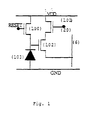
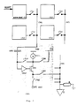
- FIG. 1 An example of an active pixel (1) containing three transistors (100),(101),(102) and a photodiode (103) that can be used in the present invention is shown in figure 1.
- Switch (20) and line (6) have the same function as the parts (21),(23),(71),(73), and (6),(56) respectively in the figures 2 and 5.
- a pulsed signal on gate “RESET” will zero the accumulated charges on the photodiode node (103), i.e. its forces the pixels in a "reference state".
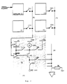
- a device to readout active pixels or parts of an imager with active pixels is the scheme represented in figure 2.
- an arbitrary array of 2 by 2 active pixels (1),(2),(3),(4) is drawn with one column amplifier (in this text also referred to as the amplifying circuit) (5).
- Said column amplifier (5) may as well be integrated within each pixel (1),(2),(3),(4), so as to form a more elaborate active pixel in its own, at the cost of area.
- This integration may be a preferred option for imaging devices and for a sensor device for non-optical applications which are arranged in a fashion which is not row/column wise, for instance, linear image sensor.
- the output signal of an active pixel (1),(2),(3),(4) is via an optional switch (21),(22),(23),(24) read out over a line (6), (7) and is passed to a common output bus (8) via an optional switch (25).
- Non-uniformities of different signals on the different lines (6) and (7) of different such column amplifiers (5) are compensated at the output bus (8).
- the relative offsets of the input signals (6) and (7), including the offset non-uniformity induced by the output transistor (in this text also referred to as the amplifying element) (9) itself, is compensated by adjusting an offset compensation input of a second amplifier (11). This adjustment or calibration is carried out while forcing the active pixel that is being read out, or the signal on line (6) or (7) in general, to a reference state.
- the Source of transistor (9) is thus forced to a known voltage (30).
- This known voltage (30) can be a supply voltage of the imaging device and is preferably common for all columns of the matrix of pixels.
- the voltage at the drain and gate of the transistor (9) will settle to an equilibrium value.
- One can predict the behavior of such circuits by the use of analog circuit simulators such as HSpice, commercialized by the company Metasoft.
- the offset needed to accomplish the equilibrium is stored in an analog memory which is represented as a capacitor (10) and a switch (27).
- Other ways to implement analog memory known to the man skilled in the art, can be used for this purpose too.
- switches (27) and (26) are opened.
- Switch (28) is closed to allow for a large supply current for transistor (9).
- the optional switch (25) is used for each column amplifier (5) separately to connect to the bus (8) in sequential or in a random addressed manner.
- the multiplexing done in this way through switch (25) may as well be accomplished in different ways.
- the transistor (9) is preferably a MOSFET, but other types of active elements like bipolar transistors or thyristors, or JFETs are also appropriate.
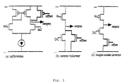
- the second amplifier (11),(61) in figures 2, 5 respectively is generic. Many known types of amplifiers can be used for this purpose, as long as there is provided means to adjust their offset voltage by an external voltage or current. Three of such second amplifiers, according to the art are shown in figure 3, with an offset adjusting means drawn in thick lines. The amplifier of figure 11 can be used for the same purpose. Note that the offset adjusting input is a voltage input in each of these cases. However, the input device is a MOSFET used as current source, so an input current could be applied as offset means directly as well. Note also that the second input of a two-input amplifier in itself can be considered also as an offset adjusting input, and can be used for that purpose.
- the second amplifier (11) is not necessarily a unity amplifier. It may include also a filter function to improve e.g. signal to noise ratio.
- the use of a source follower transistor for second amplifier (11) is a simple and straightforward implementation.
- the capacitor (10) in figure 2 is a means for analog memory.
- Other types of analog memory may be used instead, e.g. based on techniques used for the fabrication of non-volatile memories (ROM, EPROM, EEPROM), known to those skilled in the art.
- Analog memory can also be implemented by a combination of ADC and DAC and digital memory.
- the current source (12) may be implemented in well-known ways, as e.g. a MOSFET with a voltage at the gate. In this way however, the currents of different column amplifiers (5) will have different values due to non-uniformities of the electronic devices. This non-uniformity of the currents will have second order effects on the uniformity of the final outputs on the bus (8).
- One method consists in the use of one single current source for all said column amplifiers in the imaging array.
- the said single current source is applied to all column amplifiers in turn by means of switches.
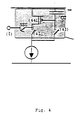
- Another method consists of the calibration of the current sources which are residing in each column amplifier during those time intervals that these currents are not in use: e.g. during the time that switch (28) in figure 2 is closed. This can be accomplished by a circuit configuration as depicted in figure 4.
- the output (I )of this subcircuit is the current source (12) depicted in figure 2.
- the switches (42) and (43) serve to connect and calibrate the MOSFET (44) for a known current level.
- Another method is the use of circuit components which are not MOSFETs and thus suffer less from non-uniformities, as resistors, Bipolar transistors or JFETs.
- FIG. 5 An implementation of the imaging device according to another preferred embodiment of the present invention is shown in figure 5.
- a matrix of 2 x 2 active pixels is drawn. Every pixel (51),(52),(53),(54) can, via a switch (71),(72), (73),(74), impose its output signal to the column lines (56),(52).
- a pixel can be switched in its reference state, e.g. via a "reset signal" (this is a common but not exclusive way to do such).
- the signal on line (56) changes. But this new signal contains the unwanted offset either via the capacitor (60) the change of this signal is applied to the gate of transistor (59), and when (75) is closed, to the output amplifier of the imaging device.
- circuit in figure 5 is a special case of the circuit in figure 2.
- the combination of (60) and (61) in figure 5 is a second amplifier with AC-coupled input. This too is to be considered as an amplifier with offset adjustment terminal.
- the real input and the offset input are at both end of the said capacitor (60).
- the active pixels to be used with this type of readout must obey only to one criterium, that they can be set in two or more different states, corresponding to different amounts of collected light, or to different signal levels in general.
- the signal path that generates the FPN should be in common for both states, i.e. pass through the same amplifying path in the pixel.
- a timing scheme of the FPN elimination method according to the present invention is shown in figure 7.
- the signals to be expected at terminals of the preferred embodiments (see figures hereabove), while reading two pixels on the same column are shown.
- the shown applied binary signals are (77),(27),(76),(26),(78),(28) and (75),(25) (which are the same for simplicity; but in combination with a multiplexer (not drawn) (75), (25) is different from (78), (28), and Reset, which sets the pixel in a reset state or not (indicated as "first state” and "second state”).
- Two analog signals are shown: (6), (56), the voltage of the column line which reflects the output of the pixel(s) connected to it, and which is the input of the column amplifier (5),(55); and the voltage at the source of transistor (9), (59), which is the output of the column amplifier (5), (55).
- the white arrows indicate the difference of the resulting signal going from pixel (1) to pixel (2).
- FIG. 8 Another embodiment of the present invention is shown in figure 8.
- a pixel incorporating a photosensitive element and an amplifying circuit comprising an amplifying element (101) and a memory element (102) is shown. Furthermore shown are connections and circuits to adjust the signal in an output terminal of said amplifying element (101) to a known level, a measure of the corresponding level in a control terminal of said amplifying element being stored on said memory element.
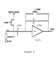
- a prior art amplifying circuit is shown in figure 9.
- the pixel shown in figure 9 advantageously is used in case the photo-current of a photosensitive element or a detector is readout by an amplifier (107) with capacitive feedback (108), which integrates this photo-current and gives an output voltage that is proportional to the photo-current and integration time.
- the integration time is determined by timing signals, the photo-current and an integration capacitor (108).
- Another (second) capacitor (106) is needed to allow the voltage (Bias minus zero-Bias) across the photo detector to be controlled in a precise way. Specific applications require such features for reasons of photometric performance.
- One operational disadvantage of the amplifying circuit of figure 9 is that, for good suppression of the parasitic effects at the input, the ratio of the capacitances of both capacitors (106) and (108) should be as large as possible.
- this ratio should be larger than 1000.
- the capacitance of said integration capacitor (108) is 1 pF as imposed by the magnitude of photo detector current.
- the second capacitor (106) should be 1 nF in such cases. Such a large capacitor cannot be integrated on chip.
- a new charge amplifying circuit making use of the present invention is therefore disclosed in figure 8.
- a pixel as shown in figure 8 is proposed.
- Said amplifying circuit is referred to as the AC-coupled direct injection circuit (ACI).
- An AC-coupled amplifier in the feedback loop (103) is used to adjust the input mode of the amplifying element (101), preferably a MOSFET transistor.
- the photo-current is integrated on a third capacitor (104).
- the column amplifier of the present invention is used in combination with a photo receptor forming thus a pixel.
- the capacitors in this embodiment may have small values, the circuit can be integrated easily on chip, as a single element or as pixel arrays. Another advantage of this circuit is that the variation and drift of the bias voltage across the photo receptor is very low.
- FIG 10. Another improvement of the AC-coupled transimpedance amplifier is shown in figure 10. This circuit is referred to as AC-regulated transimpedance amplifier (AR)
- the memory element (112) is combined with a switch "reset”.
- An amplifier (111) with an extra offset input is used as the feedback amplifier and at the same time as the amplifying element.
- the photo detector's current is integrated on the capacitor (114).
- the current is integrated on a feedback capacitor (114). Yet during reset, the zero-bias voltage is enforced on the amplifier's input (111) and the offset imbalance is stored on the capacitor (112).
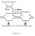
- the circuit as shown in figure 11 is an example of a differential amplifier with two negative and two positive input nodes which could be used in amplifier (111).
- circuits of figures 8 and 10 can be combined in one circuit.
- Such combined circuit AC-regulated direct injection (ARI) circuit
- the memory element (122) is a capacitor in combination with a switch S3.
- the analog signal on this memory element is the input on an additional offset correcting input of a second amplifier (123) which in turn adjust the gate voltage of the amplifying element (121).
- said pixels can be used in cryogenic readout amplifiers possibly in stressed GeGa detector arrays.
- the Germanium-Gallium (Ge:Ga) detectors should be operated at 1.6 Kelvin, at a bias voltage of 20 mV.
- the closely coupled readout electronics should be operated at the same temperature and maintained this bias with an accuracy of 0.1 mV.
Description
- The present invention relates to solid state imaging devices being manufactured in a CMOS- or MOS-technology. More particularly, an amplifying circuit and a method for eliminating fixed pattern noise in the output signal of a pixel or of an image sensor are disclosed.
- Solid state image sensors are well known. Commonly solid state image sensors are implemented in a CCD-technology or in a CMOS- or MOS-technology. Solid state image sensors find a widespread use in camera systems. In this embodiment a matrix of pixels comprising light sensitive elements constitutes an image sensor, which is mounted in the camera system. The signal of said matrix is measured and multiplexed to a so-called video-signal.
- CCD-based camera systems have less noise fluctuations in the image compared to CMOS- or MOS-based camera systems. Therefore CCD-based camera systems are nowadays preferred in applications wherein a high image quality is required such as video or still camera applications. Due to the further miniaturisation of the CMOS electronics technology, it is possible to realise complex CMOS- or MOS-based pixels as small as CCD-based pixels. It is a further advantage of CMOS- or MOS-based pixels that CMOS is a technology being offered by most foundries whereas CCD-technology is rarily offered and a more complex and expensive one.
- Of the image sensors implemented in a CMOS- or MOS-technology, CMOS or MOS image sensors with passive pixels and CMOS or MOS image sensors with active pixels are distinguished. An active pixel is configured with means integrated in the pixel to amplify the charge that is collected on the light sensitive element. Passive pixels do not have said means and require a charge-sensitive amplifier that is not integrated in the pixel and is connected with a long line towards the pixel. For this reason, active pixel image sensors are potentially less sensitive to noise fluctuations than passive pixels. Due to the additional electronics in the active pixel, an active pixel image sensor may be equipped to execute more sophisticated functions, which can be advantageous for the performance of the camera system. Said functions can include filtering, operation at higher speed or operation in more extreme illumination conditions. It remains however a main drawback of active pixel CMOS or MOS image sensors, hampering their use in applications requiring a high image quality, that their output signal has an additional non-uniformity caused by the statistical spread on the characteristics of the electronic components composing the active pixel. An example of such characteristic being subject to manufacturing process variations is the threshold voltage of MOS transistors integrated in the pixel. If no precautions are taken, this non-uniformity, called fixed pattern noise or FPN, is seen as a "snow-like" shade over the image being taken with a CMOS or MOS image sensor with active pixels.
- Document US-A-4274113 discloses a solid state imaging device having a sensor portion and a signal processing circuit. Said signal processing circuit comprises means to eliminate fixed pattern noise. In this device the charge collected on a passive pixel is measured on a common charge amplifier. The pixel is sampled two times consecutively, and the difference of charges is constituting the signal. The first sampling is taken with the pixel not connected to the output, the second sampling is taken with the pixels connected to the output for a short time, so that the charge is integrated in the output. This method to eliminate FPN however is not suited for active pixels which have not a charge output, but which have a voltage output or current output or similar. Also, as disclosed in the preferred embodiment of US-4274113, reading charge over a large bus with high capacitance deteriorates the temporal noise in the final sensor image.
- Document US-A-4809074 discloses a solid state imager having a signal processing circuit for reducing noise, in particular FPN. Each pixel has two switches, which makes it possible to read a pixel charge with less noise and FPN than in pixels with only one switch. The FPN cancellation is performed by reading twice the charge on the output node. Again, the method disclosed in this patent is not suited for active pixel imaging sensors.
- The patent application WO92/16999 discloses a circuit for minimising the variation in characteristics across different parts of an imaging device caused by manufacturing process variations between a plurality of inverting amplifiers in said imaging device. Said circuit comprises at least one transistor connected in series with a power supply terminal on each of the inverting amplifiers so as to provide a new reference level for each inverting amplifier whereby the switching threshold of the inverting amplifier is controllable by a voltage applied to a control input connection of said transistor. This method applies only for an imaging device with passive pixels.
- Document EP-A-0665685 discloses an active pixel image sensor. This patent describes a method to cancel non-uniformity of the pixel response. This method is based on the fact that all pixels outputs are fed through switches and column/row buses to a common output, without passing trough intermediate (column) buffers. This method is viable, but it requires the output stage of every individual pixel to be powerful enough to drive the buses/output lines at a high readout speed. The proposed method furthermore adds additional fixed pattern noise by the multiplexing structures.
- Document US-A-4 580 103 discloses an amplifying circuit for amplifying an input ac signal thereby aiming to eliminate the offset present in the input ac signal and thereby amplifying the inherent input amplifier offset with a gain of about unity. The circuit as disclosed in D1 does not remove the inherent offset of the amplifier (amplifying element) of the amplifying circuit but reduces this offset influence on the output signal by amplifying the input signal more strongly and holding the gain of the offset at a factor of about one. Thus the offset errors induced by the amplifying element are reduced but remain.
- Document IBM TDB, Vol. 23, No. 9, pp. 4195-4196 discloses an amplifier circuit that introduces means for reducing offset error voltages of amplifiers in the circuit. The offset error is reduced but is not suppressed; moreover one can note that the output voltage of the amplifying circuit is influenced by the offset of one of the amplifiers. The amplifier circuit furthermore can not be forced to an externally predetermined uniform offset correction.
- Document US-A-5 321 528 provides an image sensor chip which includes means for generating a signal allowing the offset voltage within a chip to be separated and compensated for by another circuit wherein the chip is later integrated. Thus a signal can be generated that excludes an image signal but includes an offset level. The further processing of such signal is to occur on an image sensor per image sensor basis.
- Document US-A-5 296 696 discloses an amplifier circuit for reducing Fixed Pattern Noise (FPN) in an image taken with a pixel array, the FPN being caused by the imaging circuit. The amplifier circuit however introduces an offset caused by the amplifying element 16. Thus there will remain a source of FPN in the final image caused by the amplifying element and this FPN will be different for at least each column of a pixel array.
- The present invention discloses a device such as an image sensor which permits to reduce fixed pattern noise (FPN) which is invariant in time, without introducing noise of other origin. This device comprises a matrix of active pixels as well as electronic components or circuits located by preference at the edges or border of the matrix of pixels. At the expense of forming an image sensor with an unusual large area, said electronic components or circuits can also be integrated in said pixels. Said electronic components or circuits comprise at least one amplifying circuit which is common to a group of pixels such as a column or a row in said matrix. Furthermore, said device has an output line that is preferably common to said matrix. The amplifying circuit comprises an amplifying element and a memory element that are connected to circuitry that is provided to change the signal in the output terminal of said amplifying element to a known level, and to store the corresponding level, or a measure thereof, in the control terminal of said amplifying element on said memory element.
- The active pixels are adapted for being brought in a state corresponding to an amount of radiation collected on said pixel, and can therefore be changed in to a first state. It is required that this first state can be compared to a second state that is different. Said first state can correspond to an amount of collected radiation or light on the radiation or light sensitive element in said pixel. Said first state can also correspond to the reset state of the pixels or to a non-illuminated or dark condition of the pixel. Said second state can correspond to a non-illuminated or dark condition of the pixel, or to an amount of collected radiation or light on the radiation or light sensitive element in said pixel, or to the reset state of the pixel.
- Preferably, the amplifying element is a transistor and more particularly of the type of metal oxide semiconductor transistors wherein said output terminal is the source or the drain of the transistor and wherein the control terminal is the gate of said transistor. It also can be a more complex amplifier in its own. The memory element is preferably a capacitor or a nonvolatile memory element as used in ROMs, EPPROMs, EEPROMs, or flash EEPROMs.
- In a first aspect of the present invention, an amplifying circuit is disclosed, comprising:
- an amplifying element having an output terminal and a control terminal, and said amplifying element including a transistor;
- a memory element;
- Preferably, said externally predetermined voltage is directly forced on the output terminal through a switch or a resistor or a current source or a device that can keep the output terminal at said predetermined voltage.
- Preferably, said memory element is an analog memory element or a non-volatile memory element as used in analog EPROMS, EEPROMS or flash EEPROMS, and more particularly a capacitor.
Preferably, the means mentioned hereabove are adjusting/forcing circuits. - According to a preferred embodiment, a predetermined voltage level is directly applied on said output terminal and wherein said corresponding voltage level is indirectly adjusted on the control terminal of said amplifying element by circuit functioning of said means. Preferably, said amplifying element is a transistor, said output terminal being the source or drain of said transistor, and said control terminal being the gate of said transistor. Said transistor is preferably a transistor of the type of metal oxide semiconductor transistors.
- In a second aspect of the present invention, a pixel, adapted for integration in an imaging device, comprising the amplifying circuit as hereabove described and further comprising a radiation sensitive element is disclosed.
- According to a preferred embodiment, said pixel further comprises an AC-coupled amplifier with a capacitive feedback circuit in between said amplifying element and said memory element.
- According to another preferred embodiment, said pixel has an amplifying element with a first terminal being connected to said photosensitive element and a control terminal being connected to said memory element, a second terminal of said amplifying element being connected through a capacitor with said first terminal.
- In a third aspect of the present invention, a device for imaging applications comprising the amplifying circuit as hereabove described is disclosed. Said device comprises:
- a matrix of active pixels arranged in a geometric configuration, said pixels yielding electrical signal outputs generated by photoelectric conversion, and being adapted for being brought in a state corresponding to an amount of radiation collected on said pixels;
- at least one amplifying circuit being common to a group of pixels of said matrix; and
- an output line being common to the matrix of pixels.
- Preferably, said matrix is arranged in columns and rows and wherein each amplifying circuit is common to a group of pixels such as a column or a row in said matrix. Preferably, said predetermined level is common for essentially all columns of said matrix.
- In a fourth aspect of the present invention, a method is disclosed for eliminating fixed pattern noise which is invariant in time, in the output signal of an image sensor, making use of said device.
- The method is as follows:
- reading out the signal of a pixel in a first state while forcing directly an externally predetermined offset correction voltage on the output terminal of an amplifying element, thereby defining a corresponding voltage level on the control terminal of said amplifying element and storing said corresponding voltage level or a measure thereof on a memory element that is connected to said pixel, and thereby defining a first voltage at the output of said amplifying element;
- subtracting said first voltage at the output of said amplifying element of a second voltage at the output of said amplifying element, said second voltage being defined by the output signal of the same pixel in a second state and said second voltage including the voltage level stored on said memory element, whereby the output voltage of the amplifying element shifts proportionally to the difference of the signal of said pixel in said first and said second state;
- transferring the subtracted signal to an output line that is common for said group; and
- repeating this operation for all or part of pixels of the imaging device.
- Preferably, said externally predetermined voltage is directly forced on the output terminal through a switch or a resistor or a current source or a device that can keep the output terminal at said predetermined voltage.
- Preferably, said first and second state of said pixel are read out consecutively. More preferably, said first state or said second state corresponds to an amount of radiation or light collected on the light sensitive element in said pixel or to the dark condition of said pixel or to the reset state of said pixel. Said predetermined output voltage level is derived from a supply voltage of said solid state imaging device.
- The voltage level stored in the memory element includes preferably the offset voltage of said amplifying element.
- In a fifth aspect of the present invention, the use is disclosed of said imaging device and said method in camera systems and in imaging applications requiring a high image quality. An example of such camera system is a video or still camera or a camera integrated in a multimedia device such as a Personal Computer equipped with video functionality or with video and speech functionality.
-
- Figure 1
- shows an example of an active pixel containing three transistors, and a photodiode that can be used in the present invention.
- Figure 2
- shows an embodiment of the device for imaging applications according to the present invention.
- Figure 3
- shows three amplifiers that can be integrated as components (11), (61), (103), (111), (123) in the device for imaging applications according to the present invention.
- Figure 4
- shows current sources that can be used in the column amplifiers of the device for imaging applications according to the present invention.
- Figure 5
- shows another embodiment of the device for imaging applications according to the present invention.
- Figure 6
- shows two pixels of a structure that could be part of an array shown in figure 2 or 5.
- Figure 7
- schematically shows the timing diagram of the method for eliminating fixed pattern noise in a solid sate imaging device according to the present invention.
- Figure 8
- shows an embodiment (further referred to as ACI) of the present invention with the amplifying circuit in connection with a photosensitive element.
- Figure 9
- shows a prior art amplifying circuit
- Figure 10
- shows another embodiment (further referred to as AR) of the present invention with the amplifying circuit in connection with a photosensitive element.
- Figure 11
- shows a differential amplifier with similar use as the amplifiers of figure 3.
- Figure 12
- shows another embodiment (further referred to as ARI) of the present invention with the amplifying circuit in connection with a photosensitive element.
- In the sequel and for the purpose of teaching only an implementation of the image sensor as a sensor with nxm pixels in a double metal, single poly 0.7 µm CMOS process can be assumed. The size of such image sensor with 384x288 pixels is 6,3x5,7 mm. The dimensions of the light sensitive elements in the photodiodes of the pixels are 14x14 µm. Photodiodes of this size generate currents of about 1 nA at light illumination level of lmW/cm2. It is obvious that these numbers represent only one option within the art and that many other implementations will be evident for those skilled in the art. An example of an active pixel (1) containing three transistors (100),(101),(102) and a photodiode (103) that can be used in the present invention is shown in figure 1. Switch (20) and line (6) have the same function as the parts (21),(23),(71),(73), and (6),(56) respectively in the figures 2 and 5. A pulsed signal on gate "RESET" will zero the accumulated charges on the photodiode node (103), i.e. its forces the pixels in a "reference state".
- A device to readout active pixels or parts of an imager with active pixels is the scheme represented in figure 2. In this figure an arbitrary array of 2 by 2 active pixels (1),(2),(3),(4) is drawn with one column amplifier (in this text also referred to as the amplifying circuit) (5). Said column amplifier (5) may as well be integrated within each pixel (1),(2),(3),(4), so as to form a more elaborate active pixel in its own, at the cost of area. This integration may be a preferred option for imaging devices and for a sensor device for non-optical applications which are arranged in a fashion which is not row/column wise, for instance, linear image sensor.
- The output signal of an active pixel (1),(2),(3),(4) is via an optional switch (21),(22),(23),(24) read out over a line (6), (7) and is passed to a common output bus (8) via an optional switch (25). Non-uniformities of different signals on the different lines (6) and (7) of different such column amplifiers (5) are compensated at the output bus (8). The relative offsets of the input signals (6) and (7), including the offset non-uniformity induced by the output transistor (in this text also referred to as the amplifying element) (9) itself, is compensated by adjusting an offset compensation input of a second amplifier (11). This adjustment or calibration is carried out while forcing the active pixel that is being read out, or the signal on line (6) or (7) in general, to a reference state.
- For adjustment or calibration, switches (27) and (26) are closed. The Source of transistor (9) is thus forced to a known voltage (30). This known voltage (30) can be a supply voltage of the imaging device and is preferably common for all columns of the matrix of pixels. With appropriate circuit components and applied voltages and currents, which are straightforward for those skilled in the art, the voltage at the drain and gate of the transistor (9) will settle to an equilibrium value. One can predict the behavior of such circuits by the use of analog circuit simulators such as HSpice, commercialized by the company Metasoft. The offset needed to accomplish the equilibrium is stored in an analog memory which is represented as a capacitor (10) and a switch (27). Other ways to implement analog memory, known to the man skilled in the art, can be used for this purpose too. For the normal read out operation, the switches (27) and (26) are opened. Switch (28) is closed to allow for a large supply current for transistor (9). The optional switch (25) is used for each column amplifier (5) separately to connect to the bus (8) in sequential or in a random addressed manner.
- The multiplexing done in this way through switch (25) may as well be accomplished in different ways.
- The transistor (9) is preferably a MOSFET, but other types of active elements like bipolar transistors or thyristors, or JFETs are also appropriate. The second amplifier (11),(61) in figures 2, 5 respectively is generic. Many known types of amplifiers can be used for this purpose, as long as there is provided means to adjust their offset voltage by an external voltage or current. Three of such second amplifiers, according to the art are shown in figure 3, with an offset adjusting means drawn in thick lines. The amplifier of figure 11 can be used for the same purpose. Note that the offset adjusting input is a voltage input in each of these cases. However, the input device is a MOSFET used as current source, so an input current could be applied as offset means directly as well. Note also that the second input of a two-input amplifier in itself can be considered also as an offset adjusting input, and can be used for that purpose.
- The second amplifier (11) is not necessarily a unity amplifier. It may include also a filter function to improve e.g. signal to noise ratio. The use of a source follower transistor for second amplifier (11) is a simple and straightforward implementation.
- The capacitor (10) in figure 2 is a means for analog memory. Other types of analog memory may be used instead, e.g. based on techniques used for the fabrication of non-volatile memories (ROM, EPROM, EEPROM), known to those skilled in the art. Analog memory can also be implemented by a combination of ADC and DAC and digital memory.
- The current source (12) may be implemented in well-known ways, as e.g. a MOSFET with a voltage at the gate. In this way however, the currents of different column amplifiers (5) will have different values due to non-uniformities of the electronic devices. This non-uniformity of the currents will have second order effects on the uniformity of the final outputs on the bus (8). One can implement means to obtain more uniform or reproducible current sources (12). Those skilled in the art are aware about many such methods been devised in the past, e.g. for the fabrication of analog-digital convertors or digital-analog convertors.
- One method consists in the use of one single current source for all said column amplifiers in the imaging array. The said single current source is applied to all column amplifiers in turn by means of switches.
- Another method consists of the calibration of the current sources which are residing in each column amplifier during those time intervals that these currents are not in use: e.g. during the time that switch (28) in figure 2 is closed. This can be accomplished by a circuit configuration as depicted in figure 4. The output (I )of this subcircuit is the current source (12) depicted in figure 2. The switches (42) and (43) serve to connect and calibrate the MOSFET (44) for a known current level. Another method is the use of circuit components which are not MOSFETs and thus suffer less from non-uniformities, as resistors, Bipolar transistors or JFETs.
- An implementation of the imaging device according to another preferred embodiment of the present invention is shown in figure 5. A matrix of 2 x 2 active pixels is drawn. Every pixel (51),(52),(53),(54) can, via a switch (71),(72), (73),(74), impose its output signal to the column lines (56),(52).
- A pixel can be switched in its reference state, e.g. via a "reset signal" (this is a common but not exclusive way to do such).
- During the first of the two states, switches (77) and (76) are closed, and (78) and (75) remain open. The current source (62) delivers a small fixed current. For this reason, the source of MOSFET (59) comes to a fixed potential, and the gate of this MOSFET is forced to an equilibrium value. This value is memorised on the capacitor (60). The amplifier (61) at the gate of the MOSFET is not absolutely necessary, it may be shunted.
- The possibly unwanted offset of the pixel signal stands now over the capacitor (60).
- Before the second phase, the switches (77) and (76) are opened, and (78) and (75) potentially too are closed. Consequently, on the source of the MOSFET (59) appears the signal that was there already during the first phase, except from a small fixed shift. This signal is offered to the common output amplifier "U" of the imaging device, which does not contribute to the FPN because it is common to the whole matrix.
- During the second of the two states of the active pixel, the signal on line (56) changes. But this new signal contains the unwanted offset either via the capacitor (60) the change of this signal is applied to the gate of transistor (59), and when (75) is closed, to the output amplifier of the imaging device.
- Many column amplifiers are in parallel on the output bus (58). One can then scan these amplifiers by activating their respective switches (75).
- We draw the attention to the fact that the circuit in figure 5 is a special case of the circuit in figure 2. The combination of (60) and (61) in figure 5 is a second amplifier with AC-coupled input. This too is to be considered as an amplifier with offset adjustment terminal. The real input and the offset input are at both end of the said capacitor (60).
- In fact the variant of the circuit in figure 2, where amplifier (11) is just a short circuit, thus the said combination of (60) and (61) being only a capacitor, should be considered for this reason as trivial case of an amplifier with offset correction too. This may be sufficient for the required functionality.
- Other embodiments of the present invention are described in the sequel.
- The active pixels to be used with this type of readout must obey only to one criterium, that they can be set in two or more different states, corresponding to different amounts of collected light, or to different signal levels in general. The signal path that generates the FPN should be in common for both states, i.e. pass through the same amplifying path in the pixel. Obvious variants are:
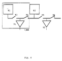
- Not limited to a simple pixel. An active pixel may be constructed so as to take its signal from different places and times, as e.g. from different photodiodes that may be shared with other active pixels, or from information that is acquired at different times. Such array is shown in figure 6 in a most simple form. Two pixels of an array are shown, only relevant parts of the pixels are shown: (81),(82) are photo detectors, (91), (92) are schematic representations of the amplifying part of the pixel.
- The switches (83), and (84) are closed and open respectively. Either one of the detectors (81) or (82)is tied to the amplifier (91) (and similarly for all other members of the array). The reference state for such a reading may be during the time that (81) is tied to (91), and the reading state is then during the time that (82) is tied to (91). Somewhere down the signal path the output of (91) is corrected using the amplifying circuit (5) as shown in figure 2. The function that is realised in this particular way is a spatio-temporal filter where the intensity at one pixel at one time is subtracted from the intensity of another pixel at another time. Several pixels in a neighbourhood could be tied at the same node, at the same or different times, thus realising more complex spatio-temporal filters. In principle the rectangles (81) and (82) may represent active pixels themselves, thus creating a hierarchic structure.
- An array may be different from the classic two-dimensional (rectangular) array. E.g. a linear array, a circular, a log-polar, even a random array is possible. If the technology allows so, a 3-dimensional array may become possible. The array could be made up of other types of detectors than optical detectors, as sensors for electro-magnetic radiation, elementary particles, pressure waves (sound), chemicals, ...
- In figures 2 & 5, the current source (12),(62) may be replaced by a resistor, or it may be combined with switch (28), (78) in one component (note that e.g. both a current source or a switch can be realized with a MOSFET)
- As mentioned before, second amplifier (11),(61) may be omitted (shunted). The circuit could be tuned to operate without second amplifier (11),(61) or it may include also filtering or a voltage offset which may contribute to a better operation (high speed, low noise, operation in required voltage range etc.).
- Switch (26), (76) in figures 2 & 5 may be replaced by a current source or a resistance or any device that can keep the source of (9),(59) at a certain voltage that must not be explicitly applied.
- In the above disclosure for simplicity it is supposed that the active pixels (1),(2),(3),(4),(51),(52),(53), (54) output is a voltage. In practice, an active pixel may output its signal via a transistor, of which the load is common for the bus, and resides outside the pixel. The transistor together with the external load element (being a passive component like a resistor, or an active component like a MOSFET), is a transistor amplifier, typically a source follower, an inverting amplifier, or a differential amplifier.
- It is obvious that active pixels (1),(2),(3),(4),(51),(52),(53),(54) which output a current instead of a voltage may be used as well. A current may be converted to a voltage over a resistor or a switched capacitor.
- It is obvious that, wherever MOSFETs are mentioned in this text, other types of controlled amplification devices can be thought, as far as they can realise the same functions, as bipolar transistors or J-FETs.
- As the difference between active pixel and passive pixel lies merely in the presence of an amplifying element in the pixel, the method may be applied to cancel the FPN of passive pixels too. For this purpose the charges of the passive pixel can first be converted.
- It is possible to realise an FPN-free reading of an active pixel array in other ways:
- by reading the said two states separately and doing the subtraction outside the imaging device, in analog or in digital mode after AD-conversion. Such an approach requires a double readout speed, and some kind of analog or digital memory.
- by using other types of differential amplifiers at the column edges. The signals of the two states may be stored on a capacitor, and the differential amplifier read the difference. This is a viable way of reading the active pixel signal, and removing the FPN of the active pixels, but it does not cancel FPN that is generated in the differential amplifier itself.
- A timing scheme of the FPN elimination method according to the present invention is shown in figure 7. The signals to be expected at terminals of the preferred embodiments (see figures hereabove), while reading two pixels on the same column are shown. The shown applied binary signals are (77),(27),(76),(26),(78),(28) and (75),(25) (which are the same for simplicity; but in combination with a multiplexer (not drawn) (75), (25) is different from (78), (28), and Reset, which sets the pixel in a reset state or not (indicated as "first state" and "second state"). Two analog signals are shown: (6), (56), the voltage of the column line which reflects the output of the pixel(s) connected to it, and which is the input of the column amplifier (5),(55); and the voltage at the source of transistor (9), (59), which is the output of the column amplifier (5), (55). The white arrows indicate the difference of the resulting signal going from pixel (1) to pixel (2).
- Another embodiment of the present invention is shown in figure 8. A pixel incorporating a photosensitive element and an amplifying circuit comprising an amplifying element (101) and a memory element (102) is shown. Furthermore shown are connections and circuits to adjust the signal in an output terminal of said amplifying element (101) to a known level, a measure of the corresponding level in a control terminal of said amplifying element being stored on said memory element. A prior art amplifying circuit is shown in figure 9.
- The pixel shown in figure 9 advantageously is used in case the photo-current of a photosensitive element or a detector is readout by an amplifier (107) with capacitive feedback (108), which integrates this photo-current and gives an output voltage that is proportional to the photo-current and integration time. The integration time is determined by timing signals, the photo-current and an integration capacitor (108). Another (second) capacitor (106) is needed to allow the voltage (Bias minus zero-Bias) across the photo detector to be controlled in a precise way. Specific applications require such features for reasons of photometric performance. One operational disadvantage of the amplifying circuit of figure 9 is that, for good suppression of the parasitic effects at the input, the ratio of the capacitances of both capacitors (106) and (108) should be as large as possible. In some cases, this ratio should be larger than 1000. Yet for some applications, the capacitance of said integration capacitor (108) is 1 pF as imposed by the magnitude of photo detector current. Thus, the second capacitor (106) should be 1 nF in such cases. Such a large capacitor cannot be integrated on chip.
- A new charge amplifying circuit making use of the present invention is therefore disclosed in figure 8.
- In order to overcome the need of a large number of discrete capacitors in the circuit of figure 9, a pixel as shown in figure 8 is proposed. Here, an amplifying circuit based on the present invention is presented. Said amplifying circuit is referred to as the AC-coupled direct injection circuit (ACI). An AC-coupled amplifier in the feedback loop (103) is used to adjust the input mode of the amplifying element (101), preferably a MOSFET transistor. The photo-current is integrated on a third capacitor (104). The column amplifier of the present invention is used in combination with a photo receptor forming thus a pixel. As the capacitors in this embodiment may have small values, the circuit can be integrated easily on chip, as a single element or as pixel arrays. Another advantage of this circuit is that the variation and drift of the bias voltage across the photo receptor is very low.
- Another improvement of the AC-coupled transimpedance amplifier is shown in figure 10. This circuit is referred to as AC-regulated transimpedance amplifier (AR)
- Here, the drawback of using a large second capacitor is solved by using an amplifying circuit according to the present invention. The memory element (112) is combined with a switch "reset". An amplifier (111) with an extra offset input is used as the feedback amplifier and at the same time as the amplifying element. The photo detector's current is integrated on the capacitor (114).
- As a normal transimpedance amplifier configuration, the current is integrated on a feedback capacitor (114). Yet during reset, the zero-bias voltage is enforced on the amplifier's input (111) and the offset imbalance is stored on the capacitor (112).
- The circuit as shown in figure 11 is an example of a differential amplifier with two negative and two positive input nodes which could be used in amplifier (111).
- The circuits of figures 8 and 10 can be combined in one circuit. Such combined circuit (AC-regulated direct injection (ARI) circuit) is represented in figure 12. The memory element (122) is a capacitor in combination with a switch S3. The analog signal on this memory element is the input on an additional offset correcting input of a second amplifier (123) which in turn adjust the gate voltage of the amplifying element (121).
- This circuit combines the following advantages:
- precise control of the BIAS-ZERO BIAS voltage over the photo detector,
- no need for large capacitor, the amplifier can be integrated on chip in combination with a photo receptor (120)
- Advantageously, said pixels can be used in cryogenic readout amplifiers possibly in stressed GeGa detector arrays. For space applications and for low leakage applications, the Germanium-Gallium (Ge:Ga) detectors should be operated at 1.6 Kelvin, at a bias voltage of 20 mV. The closely coupled readout electronics should be operated at the same temperature and maintained this bias with an accuracy of 0.1 mV.
Claims (21)
- An amplifying circuit (5), (55) comprising:an amplifying element (9), (59), (101), (111), (121) having an output terminal and a control terminal, and said amplifying element including a transistor;a memory element (10), (60), (102), (112), (122);and being characterised in that said amplifying circuit further comprises means for forcing an externally predetermined offset correction voltage directly on the output terminal of said amplifying element, and for adjusting a corresponding voltage level on the control terminal of said amplifying element, said corresponding voltage level being determined by said predetermined voltage and by said means, and said means further having a part for storing on said memory element said corresponding voltage level or a measure of said corresponding voltage level.
- The amplifying circuit as recited in claim 1 wherein said externally predetermined voltage is directly forced on the output terminal through a switch or a resistor or a current source or a device that can keep the output terminal at said predetermined voltage.
- The amplifying circuit as recited in claim 1 wherein said memory element is an analog memory element or a non-volatile memory element as used in analog EPROMS, EEPROMS or flash EEPROMS.
- The amplifying circuit as recited in claim 3 wherein said memory element is a capacitor.
- The amplifying circuit as recited in claim 1 wherein said means are an adjusting/forcing circuit.
- The amplifying circuit as recited in claim 5 wherein said corresponding voltage level is indirectly adjusted on the control terminal of said amplifying element by circuit functioning of said means.
- The amplifying circuit as recited in claim 1, wherein said amplifying element is a transistor, said output terminal being the source or drain of said transistor, and said control terminal being the gate of said transistor.
- The amplifying circuit as recited in claim 7, wherein said transistor is a transistor of the type of metal oxide semiconductor transistors.
- A pixel, adapted for integration in an imaging device, comprising the amplifying circuit as recited in claim 1 and further comprising a radiation sensitive element.
- The pixel as recited in claim 9 further comprising an AC-coupled amplifier with a capacitive feedback circuit (103), (123) in between said amplifying element (101), (121) and said memory element (102), (122).
- The pixel as recited in claim 9, wherein said amplifying element (111) has a first terminal being connected to said photosensitive element (110) and a control terminal being connected to said memory element (112), a second terminal of said amplifying element being connected through a capacitor (114) with said first terminal.
- A device for imaging applications comprising the amplifying circuit (5),(55) as recited in claim 1 and further comprising:a matrix of active pixels (1,2,3,4), (51), (52), (53), (54) arranged in a geometric configuration, said pixels yielding electrical signal outputs generated by photoelectric conversion, and being adapted for being brought in a state corresponding to an amount of radiation collected on said pixels;at least one amplifying circuit (5), (55) being common to a group of pixels (1,2), (51), (52) of said matrix; andan output line (8), (58) being common to the matrix of pixels (1,2,3,4), (51), (52), (53), (54).
- The device as recited in claim 12, wherein said matrix is arranged in columns and rows and wherein each amplifying circuit is common to a group of pixels such as a column or a row in said matrix.
- The device as recited in Claim 13, wherein said predetermined level is common for essentially all columns of said matrix.
- A method for reducing noise in a solid state imaging device having a group of active pixels, said method comprising the steps of:reading out the signal of a pixel (1) in a first state while forcing directly an externally predetermined offset correction voltage on the output terminal of an amplifying element (9) (59) that is connected to said pixel (1), thereby defining a corresponding voltage level on the control terminal of said amplifying element and storing said corresponding voltage level or a measure thereof on a memory element (10) (60) that is connected to said pixel, and thereby defining a first voltage at the output of said amplifying element (9) (59);subtracting said first voltage at the output of said amplifying element (9) (59) of a second voltage at the output of said amplifying element (9) (59), said second voltage being defined by the output signal of the same pixel in a second state and said second voltage including the voltage level stored on said memory element, whereby the output voltage of the amplifying element (9) shifts proportionally to the difference of the signal of said pixel (1) in said first and said second state;transferring the subtracted signal to an output line that is common for said group; andrepeating this operation for all or part of pixels of the imaging device.
- The method as recited in claim 15, wherein said externally predetermined voltage is directly forced on the output terminal through a switch or a resistor or a current source or a device that can keep the output terminal at said predetermined voltage.
- The method as recited in claim 15, wherein said first and second state of said pixel are read out consecutively.
- The method as recited in claim 15, wherein said first state or said second state corresponds to an amount of radiation or light collected on the light sensitive element in said pixel or to the dark condition of said pixel or to the reset state of said pixel.
- The method as recited in any one of the claims 15-18, wherein said predetermined output voltage level is derived from a supply voltage of said solid state imaging device.
- The method as recited in any one of the claims 15-19, wherein the voltage level stored on said memory element includes the offset voltage of said amplifying element.
- Use of the circuit or pixel or device as recited in any one of the claims 1 to 14 or of the method as recited in any one of the claims 15 to 20 for a camera system.
Applications Claiming Priority (6)
| Application Number | Priority Date | Filing Date | Title |
|---|---|---|---|
| US708795P | 1995-10-31 | 1995-10-31 | |
| US7087 | 1995-10-31 | ||
| EP96870025 | 1996-03-05 | ||
| EP96870025 | 1996-03-05 | ||
| US2634596P | 1996-09-19 | 1996-09-19 | |
| US26345 | 1996-09-19 |
Publications (3)
| Publication Number | Publication Date |
|---|---|
| EP0773669A2 EP0773669A2 (en) | 1997-05-14 |
| EP0773669A3 EP0773669A3 (en) | 1998-03-18 |
| EP0773669B1 true EP0773669B1 (en) | 2000-01-12 |
Family
ID=27237889
Family Applications (1)
| Application Number | Title | Priority Date | Filing Date |
|---|---|---|---|
| EP96870133A Expired - Lifetime EP0773669B1 (en) | 1995-10-31 | 1996-10-29 | Circuit, pixel, device and method for reducing fixed pattern noise in solid state imaging devices |
Country Status (3)
| Country | Link |
|---|---|
| US (1) | US20010010551A1 (en) |
| EP (1) | EP0773669B1 (en) |
| DE (1) | DE69606147T2 (en) |
Cited By (2)
| Publication number | Priority date | Publication date | Assignee | Title |
|---|---|---|---|---|
| US7750958B1 (en) | 2005-03-28 | 2010-07-06 | Cypress Semiconductor Corporation | Pixel structure |
| US7808022B1 (en) | 2005-03-28 | 2010-10-05 | Cypress Semiconductor Corporation | Cross talk reduction |
Families Citing this family (34)
| Publication number | Priority date | Publication date | Assignee | Title |
|---|---|---|---|---|
| US5953060A (en) * | 1995-10-31 | 1999-09-14 | Imec Vzw | Method for reducing fixed pattern noise in solid state imaging devices |
| US6469740B1 (en) * | 1997-02-04 | 2002-10-22 | Matsushita Electric Industrial Co., Ltd. | Physical quantity distribution sensor and method for driving the same |
| US6815791B1 (en) | 1997-02-10 | 2004-11-09 | Fillfactory | Buried, fully depletable, high fill factor photodiodes |
| US5920345A (en) * | 1997-06-02 | 1999-07-06 | Sarnoff Corporation | CMOS image sensor with improved fill factor |
| US7289148B1 (en) | 1997-09-22 | 2007-10-30 | Cypress Semiconductor Corporation (Belgium) Bvba | Devices and methods for improving the image quality in an image sensor |
| US8063963B2 (en) | 1998-02-09 | 2011-11-22 | On Semiconductor Image Sensor | Imaging device having a pixel structure with high dynamic range read-out signal |
| US7106373B1 (en) | 1998-02-09 | 2006-09-12 | Cypress Semiconductor Corporation (Belgium) Bvba | Method for increasing dynamic range of a pixel by multiple incomplete reset |
| KR100265364B1 (en) * | 1998-06-27 | 2000-09-15 | 김영환 | Cmos image sensor with wide dynamic range |
| US6781624B1 (en) | 1998-07-30 | 2004-08-24 | Canon Kabushiki Kaisha | Signal processing apparatus |
| DE69822459T2 (en) * | 1998-09-10 | 2005-01-20 | Agilent Technologies, Inc. (n.d.Ges.d.Staates Delaware), Palo Alto | Photodiode array |
| JP4326050B2 (en) * | 1998-09-22 | 2009-09-02 | ハイスペック合資会社 | High-speed image sensor |
| US7268809B2 (en) | 1998-09-23 | 2007-09-11 | San Disk Corporation | Analog buffer memory for high-speed digital image capture |
| US6760068B2 (en) * | 1998-12-31 | 2004-07-06 | Sandisk Corporation | Correction of corrupted elements in sensors using analog/multi-level non-volatile memory |
| US6677996B1 (en) * | 1999-04-21 | 2004-01-13 | Pictos Technologies, Inc. | Real time camera exposure control |
| US6844897B1 (en) * | 1999-06-15 | 2005-01-18 | Micron Technology, Inc. | Active pixel sensor (APS) readout structure with amplification |
| US6888568B1 (en) * | 1999-08-19 | 2005-05-03 | Dialog Semiconductor Gmbh | Method and apparatus for controlling pixel sensor elements |
| US8310577B1 (en) | 1999-08-19 | 2012-11-13 | Youliza, Gehts B.V. Limited Liability Company | Method and apparatus for color compensation |
| US6393098B1 (en) | 1999-08-31 | 2002-05-21 | General Electric Company | Amplifier offset and gain correction system for X-ray imaging panel |
| JP4181703B2 (en) * | 1999-09-02 | 2008-11-19 | キヤノン株式会社 | Photoelectric conversion device |
| GB9929501D0 (en) | 1999-12-14 | 2000-02-09 | Koninkl Philips Electronics Nv | Image sensor |
| DE10006525C2 (en) * | 2000-02-15 | 2002-01-24 | Micronas Munich Gmbh | Exposure sensor cell |
| US7268815B1 (en) | 2000-10-06 | 2007-09-11 | Cypress Semiconductor Corporation (Belgium) Bvba | Differential readout of a pixel array with elimination of pixel- and column-wise fixed pattern noise |
| WO2002080376A2 (en) | 2001-03-29 | 2002-10-10 | Given Imaging Ltd. | A method for timing control |
| DE10301598A1 (en) * | 2002-09-13 | 2004-03-25 | Conti Temic Microelectronic Gmbh | Photodetector structure for e.g. 3D telemetric image cameras for motor vehicles, has a photodetector unit to record and determine a photoelectric current and an integrated unit to compensate for unwanted signal portions |
| GB0224770D0 (en) * | 2002-10-24 | 2002-12-04 | Council Cent Lab Res Councils | Imaging device |
| JP2005026805A (en) * | 2003-06-30 | 2005-01-27 | Renesas Technology Corp | Semiconductor integrated circuit |
| US7046284B2 (en) * | 2003-09-30 | 2006-05-16 | Innovative Technology Licensing Llc | CMOS imaging system with low fixed pattern noise |
| JP4018644B2 (en) * | 2004-01-29 | 2007-12-05 | キヤノン株式会社 | Photoelectric conversion device and imaging system using the same |
| KR100604865B1 (en) * | 2004-06-08 | 2006-07-26 | 삼성전자주식회사 | An Active Pixel Sensor cells having improved signal to noise ratio |
| US7313288B2 (en) | 2005-04-20 | 2007-12-25 | Cypress Semiconductor Corporation | Defect pixel correction in an image sensor |
| US8094223B1 (en) | 2007-05-30 | 2012-01-10 | On Semiconductor Trading Ltd. | Bus driving in an image sensor |
| US8476567B2 (en) | 2008-09-22 | 2013-07-02 | Semiconductor Components Industries, Llc | Active pixel with precharging circuit |
| US10580809B2 (en) * | 2016-12-07 | 2020-03-03 | Stmicroelectronics (Grenoble 2) Sas | Image sensor with improved settling time |
| JP7076649B2 (en) * | 2018-10-04 | 2022-05-27 | レイセオン カンパニー | Automatic zero of buffered direct injection pixels |
Family Cites Families (7)
| Publication number | Priority date | Publication date | Assignee | Title |
|---|---|---|---|---|
| JPS55105480A (en) | 1979-02-07 | 1980-08-13 | Hitachi Ltd | Solid state pickup device |
| US4580103A (en) * | 1984-06-22 | 1986-04-01 | At&T Bell Laboratories | Amplifier circuit arrangement for eliminating input signal offset in the output |
| DE3719967A1 (en) | 1986-06-16 | 1987-12-17 | Hitachi Ltd | SOLID BODY IMAGE CONVERTER |
| JP2931088B2 (en) * | 1990-11-30 | 1999-08-09 | キヤノン株式会社 | Multi-chip type photoelectric conversion device |
| WO1992016999A1 (en) | 1991-03-13 | 1992-10-01 | Vlsi Vision Limited | Apparatus for compensating manufacturing process variation |
| JP2965777B2 (en) * | 1992-01-29 | 1999-10-18 | オリンパス光学工業株式会社 | Solid-state imaging device |
| JP3277056B2 (en) * | 1993-12-09 | 2002-04-22 | シャープ株式会社 | Signal amplification circuit and image display device using the same |
-
1996
- 1996-10-29 DE DE69606147T patent/DE69606147T2/en not_active Expired - Fee Related
- 1996-10-29 EP EP96870133A patent/EP0773669B1/en not_active Expired - Lifetime
- 1996-10-31 US US08/742,241 patent/US20010010551A1/en not_active Abandoned
Cited By (2)
| Publication number | Priority date | Publication date | Assignee | Title |
|---|---|---|---|---|
| US7750958B1 (en) | 2005-03-28 | 2010-07-06 | Cypress Semiconductor Corporation | Pixel structure |
| US7808022B1 (en) | 2005-03-28 | 2010-10-05 | Cypress Semiconductor Corporation | Cross talk reduction |
Also Published As
| Publication number | Publication date |
|---|---|
| US20010010551A1 (en) | 2001-08-02 |
| DE69606147T2 (en) | 2000-06-29 |
| DE69606147D1 (en) | 2000-02-17 |
| EP0773669A3 (en) | 1998-03-18 |
| EP0773669A2 (en) | 1997-05-14 |
Similar Documents
| Publication | Publication Date | Title |
|---|---|---|
| EP0773669B1 (en) | Circuit, pixel, device and method for reducing fixed pattern noise in solid state imaging devices | |
| US5953060A (en) | Method for reducing fixed pattern noise in solid state imaging devices | |
| US7576788B2 (en) | Image pickup apparatus including a plurality of pixels, each having a photoelectric conversion element and an amplifier whose output is prevented from falling below a predetermined level | |
| JP4362156B2 (en) | Sequential correlation double sampling method for CMOS area array sensor | |
| JP2976242B2 (en) | Integrated circuit, camera using the integrated circuit, and method for detecting incident light incident on an image sensor manufactured using the integrated circuit technology | |
| US7183531B2 (en) | Amplification with feedback capacitance for photodetector signals | |
| EP0879530B1 (en) | Current-mediated active-pixel image sensing device with current reset | |
| US8199235B2 (en) | Image sensing device and imaging system | |
| US7723661B2 (en) | Solid-state imaging device with column amplifier | |
| EP0908957A2 (en) | Image sensing apparatus, signal detection apparatus, and signal accumulation apparatus | |
| US7544921B2 (en) | Linear distributed pixel differential amplifier having mirrored inputs | |
| US8023022B2 (en) | Solid-state imaging apparatus | |
| US20080169952A1 (en) | Column-parallel sigma-delta anolog-to-digital conversion with gain and offset control | |
| JPH05207220A (en) | Solid-state image pickup device and its driving system | |
| US6822211B2 (en) | Solid-state image-sensing device | |
| US20120006973A1 (en) | Image sensor with sample and hold circuitry for addressing time variant noise | |
| JP2001339643A (en) | Black level generating circuit for solid-state image pickup device and solid-state image pickup device | |
| US7830425B2 (en) | Areal active pixel image sensor with programmable row-specific gain for hyper-spectral imaging | |
| US6642496B1 (en) | Two dimensional optical shading gain compensation for imaging sensors | |
| US20090295966A1 (en) | Solid-state imaging device and camera | |
| KR20010070481A (en) | Active pixel sensor with improved reference signal | |
| JPH11274463A (en) | Solid image pickup element | |
| US20230051657A1 (en) | Self calibrating barrier modulation pixel | |
| US7199828B2 (en) | Active pixel sensor cell array | |
| US6798452B1 (en) | Amplifying solid-state imaging device, method for driving the same and physical quantity distribution sensing semiconductor device |
Legal Events
| Date | Code | Title | Description |
|---|---|---|---|
| PUAI | Public reference made under article 153(3) epc to a published international application that has entered the european phase |
Free format text: ORIGINAL CODE: 0009012 |
|
| 17P | Request for examination filed |
Effective date: 19961119 |
|
| AK | Designated contracting states |
Kind code of ref document: A2 Designated state(s): BE CH DE FR GB IT LI NL SE |
|
| PUAL | Search report despatched |
Free format text: ORIGINAL CODE: 0009013 |
|
| AK | Designated contracting states |
Kind code of ref document: A3 Designated state(s): BE CH DE FR GB IT LI NL SE |
|
| 17Q | First examination report despatched |
Effective date: 19980717 |
|
| GRAG | Despatch of communication of intention to grant |
Free format text: ORIGINAL CODE: EPIDOS AGRA |
|
| GRAG | Despatch of communication of intention to grant |
Free format text: ORIGINAL CODE: EPIDOS AGRA |
|
| GRAH | Despatch of communication of intention to grant a patent |
Free format text: ORIGINAL CODE: EPIDOS IGRA |
|
| GRAH | Despatch of communication of intention to grant a patent |
Free format text: ORIGINAL CODE: EPIDOS IGRA |
|
| GRAA | (expected) grant |
Free format text: ORIGINAL CODE: 0009210 |
|
| AK | Designated contracting states |
Kind code of ref document: B1 Designated state(s): BE CH DE FR GB IT LI NL SE |
|
| PG25 | Lapsed in a contracting state [announced via postgrant information from national office to epo] |
Ref country code: LI Free format text: LAPSE BECAUSE OF FAILURE TO SUBMIT A TRANSLATION OF THE DESCRIPTION OR TO PAY THE FEE WITHIN THE PRESCRIBED TIME-LIMIT Effective date: 20000112 Ref country code: CH Free format text: LAPSE BECAUSE OF FAILURE TO SUBMIT A TRANSLATION OF THE DESCRIPTION OR TO PAY THE FEE WITHIN THE PRESCRIBED TIME-LIMIT Effective date: 20000112 |
|
| REG | Reference to a national code |
Ref country code: CH Ref legal event code: EP |
|
| REF | Corresponds to: |
Ref document number: 69606147 Country of ref document: DE Date of ref document: 20000217 |
|
| ET | Fr: translation filed | ||
| ITF | It: translation for a ep patent filed |
Owner name: STUDIO TORTA S.R.L. |
|
| RAP2 | Party data changed (patent owner data changed or rights of a patent transferred) |
Owner name: FILL FACTORY |
|
| REG | Reference to a national code |
Ref country code: CH Ref legal event code: PL |
|
| NLT2 | Nl: modifications (of names), taken from the european patent patent bulletin |
Owner name: FILL FACTORY |
|
| PGFP | Annual fee paid to national office [announced via postgrant information from national office to epo] |
Ref country code: BE Payment date: 20001017 Year of fee payment: 5 |
|
| PGFP | Annual fee paid to national office [announced via postgrant information from national office to epo] |
Ref country code: NL Payment date: 20001020 Year of fee payment: 5 |
|
| PGFP | Annual fee paid to national office [announced via postgrant information from national office to epo] |
Ref country code: SE Payment date: 20001024 Year of fee payment: 5 |
|
| PLBE | No opposition filed within time limit |
Free format text: ORIGINAL CODE: 0009261 |
|
| STAA | Information on the status of an ep patent application or granted ep patent |
Free format text: STATUS: NO OPPOSITION FILED WITHIN TIME LIMIT |
|
| 26N | No opposition filed | ||
| PG25 | Lapsed in a contracting state [announced via postgrant information from national office to epo] |
Ref country code: SE Free format text: LAPSE BECAUSE OF NON-PAYMENT OF DUE FEES Effective date: 20011030 |
|
| PG25 | Lapsed in a contracting state [announced via postgrant information from national office to epo] |
Ref country code: BE Free format text: LAPSE BECAUSE OF NON-PAYMENT OF DUE FEES Effective date: 20011031 |
|
| REG | Reference to a national code |
Ref country code: GB Ref legal event code: IF02 |
|
| BERE | Be: lapsed |
Owner name: INTERUNIVERSITAIR MICRO-ELEKTRONICA CENTRUM VZW Effective date: 20011031 |
|
| PG25 | Lapsed in a contracting state [announced via postgrant information from national office to epo] |
Ref country code: NL Free format text: LAPSE BECAUSE OF NON-PAYMENT OF DUE FEES Effective date: 20020501 |
|
| EUG | Se: european patent has lapsed |
Ref document number: 96870133.4 |
|
| NLV4 | Nl: lapsed or anulled due to non-payment of the annual fee |
Effective date: 20020501 |
|
| REG | Reference to a national code |
Ref country code: GB Ref legal event code: 732E |
|
| PGFP | Annual fee paid to national office [announced via postgrant information from national office to epo] |
Ref country code: GB Payment date: 20021004 Year of fee payment: 7 |
|
| PGFP | Annual fee paid to national office [announced via postgrant information from national office to epo] |
Ref country code: FR Payment date: 20021029 Year of fee payment: 7 |
|
| PG25 | Lapsed in a contracting state [announced via postgrant information from national office to epo] |
Ref country code: GB Free format text: LAPSE BECAUSE OF NON-PAYMENT OF DUE FEES Effective date: 20031029 |
|
| REG | Reference to a national code |
Ref country code: FR Ref legal event code: TP |
|
| GBPC | Gb: european patent ceased through non-payment of renewal fee |
Effective date: 20031029 |
|
| PG25 | Lapsed in a contracting state [announced via postgrant information from national office to epo] |
Ref country code: FR Free format text: LAPSE BECAUSE OF NON-PAYMENT OF DUE FEES Effective date: 20040630 |
|
| REG | Reference to a national code |
Ref country code: FR Ref legal event code: ST |
|
| PG25 | Lapsed in a contracting state [announced via postgrant information from national office to epo] |
Ref country code: IT Free format text: LAPSE BECAUSE OF NON-PAYMENT OF DUE FEES Effective date: 20051029 |
|
| PGFP | Annual fee paid to national office [announced via postgrant information from national office to epo] |
Ref country code: DE Payment date: 20061130 Year of fee payment: 11 |
|
| PG25 | Lapsed in a contracting state [announced via postgrant information from national office to epo] |
Ref country code: DE Free format text: LAPSE BECAUSE OF NON-PAYMENT OF DUE FEES Effective date: 20080501 |