EP0749089A2 - Circuit for transferring data to a print head - Google Patents
Circuit for transferring data to a print head Download PDFInfo
- Publication number
- EP0749089A2 EP0749089A2 EP96102645A EP96102645A EP0749089A2 EP 0749089 A2 EP0749089 A2 EP 0749089A2 EP 96102645 A EP96102645 A EP 96102645A EP 96102645 A EP96102645 A EP 96102645A EP 0749089 A2 EP0749089 A2 EP 0749089A2
- Authority
- EP
- European Patent Office
- Prior art keywords
- data
- input
- register
- clock
- flop
- Prior art date
- Legal status (The legal status is an assumption and is not a legal conclusion. Google has not performed a legal analysis and makes no representation as to the accuracy of the status listed.)
- Withdrawn
Links
Images

Classifications
-
- G—PHYSICS
- G06—COMPUTING; CALCULATING OR COUNTING
- G06K—GRAPHICAL DATA READING; PRESENTATION OF DATA; RECORD CARRIERS; HANDLING RECORD CARRIERS
- G06K15/00—Arrangements for producing a permanent visual presentation of the output data, e.g. computer output printers
- G06K15/02—Arrangements for producing a permanent visual presentation of the output data, e.g. computer output printers using printers
- G06K15/10—Arrangements for producing a permanent visual presentation of the output data, e.g. computer output printers using printers by matrix printers
-
- G—PHYSICS
- G06—COMPUTING; CALCULATING OR COUNTING
- G06K—GRAPHICAL DATA READING; PRESENTATION OF DATA; RECORD CARRIERS; HANDLING RECORD CARRIERS
- G06K2215/00—Arrangements for producing a permanent visual presentation of the output data
- G06K2215/0002—Handling the output data
- G06K2215/0077—Raster outputting to the print element(s)
Definitions
- the invention relates to a circuit for transferring data to a print head according to the preambles of claims 1 and 4.
- printheads - in particular thermal printheads - transmit the data to be printed out in serial form.
- Each print line to be transferred to a recording medium is converted into serial form by data word and is transferred via a data line, ie a cable, from the main board of the printer to the data input of a register attached directly to the thermal print head.
- a data line ie a cable
- the actual printing process takes place; the heating elements are activated according to the data stored in the register.
- a second cable, the synchronization line is used to synchronize the data transmission.
- Individual data are transferred from the data input to the register if and only if the state of the clock input connected to the synchronization line changes from zero One (or alternatively from one to zero) changes.
- the data contained in the register are shifted one memory cell at a time. After a number of synchronization pulses, which corresponds to the number of memory cells in the register, all memory cells are filled and the printing process is carried out.
- a disadvantage here is that the physical properties of the lines can lead to data transmission errors. Since the output resistances of conventional circuits are much higher than the characteristic impedances of the cables, it is not possible to correctly adapt the input and output resistances of the circuits used to the cables. The mismatch creates undesirable reflections at the data and clock input of the printhead, which are noticeable by exponentially decaying vibrations at the reversal points of the originally rectangular signals. It is therefore sometimes no longer possible to distinguish whether the signal at the data input is now zero or one. The disadvantageous consequence is errors in the printed image.
- the object of the present invention is to provide a circuit of the generic type which is distinguished by fast and low-error transmission of data to be printed out to the print head.
- the object is achieved in that the signals at the clock input are delayed in phase by a fixed phase angle compared to the signals at the data input.
- the main idea is to only apply a signal to the clock input when the unwanted vibrations at the data input caused by reflections have subsided. Since the clock input is delayed, i.e. phase-shifted, signals is applied, the rising or falling edge of the synchronization signal arrives only after a time-constant signal that is no longer affected by the reflections is present at the data input of the register, so that data errors are no longer possible.
- the advantages of the invention consist primarily in the fact that errors in the transmission of data to the printhead caused by reflections are no longer to be feared.
- the control circuit according to the invention is inexpensive, inexpensive to implement and reliable. It also makes it possible to increase the speed of data transmission with a reduced error rate.
- the invention can be implemented in a manner known per se by means of a parallel-serial converter.
- the latter is loaded by the microprocessor with the data to be printed out, word by word, via a data bus.
- a rectangular synchronization signal is present at a clock input of the converter, which controls the serial transmission of the data - via the data line - to the print head.
- the synchronization signal is still shifted in phase and placed on the clock input of the printhead.
- the phase shift can take place on the main circuit board of the printer or directly on the printhead and can take place, for example, by means of a low-pass filter (RC element).
- RC element low-pass filter
- the error rate of data transmission in a circuit for transmitting data to a printhead in which the data are brought into serial form by means of a parallel-serial converter and via a data line to a data input associated with the printhead Registers are transmitted, wherein a synchronization signal is applied to a clock input of the parallel-serial converter
- a flip-flop is present, in which an input state appears delayed by a clock signal at an output, that the output of the flip-flop with is connected to the data input of the register, that a data input of the flip-flop is connected to the output of the parallel-serial converter, that the output signal of an oscillator is halved in frequency and applied to the clock input of the parallel-serial converter, and that the output signal of the oscillator via a phase shifter a clock input of the flip-flop is transmitted.
- a so-called D flip-flop is used, in which the respective input state appears delayed by a clock signal at the output.
- the output of the flip-flop is connected to the data input of the register of the printhead, while the data input of the flip-flop is connected to the output of the parallel-serial converter.
- the clock input of the flip-flop and the clock input of the converter are controlled by an oscillator, which can be contained in a microprocessor - which generally controls the entire printer.
- the oscillator is connected to the clock input of the converter by a frequency bisector and also connected to the clock input of the flip-flop via a phase shifter.
- the synchronization signal present at the clock input of the converter thus has half the frequency of the signal at the clock input of the flip-flop.
- a data bit (ie a voltage that corresponds to either zero or one) is applied to the data input of the flip-flop. It is crucial here that a pulse delayed by the phase shifter arrives at the clock input of the flip-flop. The data bit present at the output of the converter is therefore only transferred to the flip-flop after a certain time has passed, so that any vibrations caused by mismatches have already subsided. At the same time, the data bit transmitted in the previous clock is present at the output of the flip-flop.
- phase shifter between the output of the oscillator and the input of the flip-flop, in addition to a low-pass filter (RC element), an inverter is particularly suitable.
- the phase shift of 180 ° caused by him corresponds to - due to the frequency halving - exactly a delay of a quarter of the cycle time of the synchronization signal at the clock input of the parallel-serial converter.
- the flip-flop can be attached in two positions. On the one hand, it can be used directly on the printhead and serve to reduce the interference (ie reflections) caused by the lines between the motherboard and the printhead. On the other hand, it can also be located near the data line connector on the printer main board and remove the reflections that occur between the parallel-serial converter and the connector.
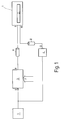
- the circuit shown in Figure 1 consists in its basic structure of a microprocessor 5, a parallel-serial converter 3 and a printhead 1.
- the latter is a thermal printhead for printing on a recording medium with a number of individually activatable heating elements which can be activated by means of a Register 2 can be controlled. Between the heating elements and a counter-pressure roller, the recording medium and - if the latter cannot be activated thermally - the effective run of an ink ribbon is arranged, so that a current flowing through the heating elements results in melting of particles of the ink ribbon and their transfer to the recording medium.
- the heating elements are activated during the printing process in accordance with the state stored by the individual elements of register 2.
- the register 2 is supplied with the data to be printed by a data line 11 through which the data are transmitted in serial form.
- the data are parallelized in the print head 1 by means of the register 2 in each case corresponding to a print line and are used for control the driver circuits of the heating elements.
- the microprocessor 5 transmits a print release signal to the print head 1, so that electrical current flows through the heating elements and a print series is printed on the recording medium .
- the data to be printed out is written into the parallel-serial converter 3 by data from the microprocessor 5 via a bus 7 (e.g. with 16 bits each).
- Clock signals of the microprocessor 5 are present at a clock input 6 of the converter 3. With each rising edge at the clock input 6, one bit is placed on an output 8 of the converter 3 and transmitted via the data line 11 to a data input 9 of the register 2.
- the clock signals of the microprocessor 5 are forwarded via a phase shifter 4, the function of which is described below, via a synchronization line 12 to a clock input 10 of the register 2.
- the state at the data input 9 is transferred to the first memory cell of the register 2 precisely when a rising edge is present at the clock input 10.
- Register 2 is thus a shift register. After a data word has been transferred to the register 2, the subsequent data words are successively written into the parallel-serial converter 3 via the bus 7 and transferred serially into the register 2 through the data line 11.
- the phase shifter 4 is provided, for example as an RC low-pass filter is feasible.
- a signal is present at its output 13, which is delayed in phase by approximately 90 ° with respect to the clock signal of the microprocessor 5.
- the phase shift thus corresponds to approximately a quarter of the clock time of the clock signal at the clock input 6 of the converter 3. Since a delayed signal is present at the clock input 10 of the register 2, the state of the data input 9 is only transferred to the register 2 after the by Vibrations caused by reflection have subsided. As a result, there is no longer any risk of data errors in register 2.
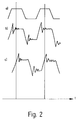
- Curve a) shows the curve shape at output 8 of parallel-serial converter 3. It is roughly rectangular with sloping flanks.
- the curve shown in b) corresponds to data input 9. Due to the mismatch of the input and output resistances of register 2 and converter 3 with the characteristic impedance of data line 11, superimposed oscillations occur on the rising and falling edges of the rectangular pulses, which decay exponentially. After a quarter of the cycle time, they have dropped to a negligible level.
- Curve c) represents the waveforms at clock input 10 of register 2. The square wave signals are also superimposed with vibrations at the reversal points. At the points in time identified by vertical lines in FIG.
- a D flip-flop 16 is used to improve the signal profiles at the data input 9.
- the state of the input 18 is around a clock signal delayed at output 19.
- the latter is connected to data input 9 of register 2 by data line 11.
- the input 18 of the flip-flop 16 is connected via a further line 20 to the output 8 of the parallel-serial converter 3.
- the clock output of the microprocessor 5 ′ is connected via a frequency bisector 14 to the clock input 6 of the parallel-serial converter 3 and the phase shifter 4, which in turn feeds the clock input 10.
- the clock frequency of the microprocessor 5 ' is therefore doubled compared to FIG. 1 with the same data transmission rate in line 11.
- phase shifter 15 is connected to the clock output of the microprocessor 5 ', the output of which feeds a clock input 17 of the flip-flop 16.
- the function of the parallel-serial converter 3, the phase shifter 4 and the register 2 correspond to the circuit shown in FIG. 1.
- the flip-flop 16 is arranged on the circuit board of the printer in the vicinity of the connection of the line 11 to the printhead; it serves to eliminate the reflections of the line 20, which is arranged between the parallel-serial converter 3 and the connection of the line 11. It would alternatively be conceivable to mount the flip-flop 16 on the print head 1, the line 11 being omitted.
- the flip-flop 16 initially takes over at a suitable time - determined by the phase shifter 15 - the state of its input 18 and transfers it to the register 2 at the second clock pulse.
- the phase shifter 15 can actually be an inverter.
- the data is then transferred into the flip-flop 16 after a quarter of a clock of the parallel-serial converter 3 has elapsed.
Abstract
Description
Die Erfindung bezieht sich auf eine Schaltung zur Übertragung von Daten auf einen Druckkopf gemäß der Oberbegriffe der Ansprüche 1 und 4.The invention relates to a circuit for transferring data to a print head according to the preambles of
Im Stande der Technik, wie er beispielsweise aus der EP-A-645 249 bekannt geworden ist, werden Druckköpfen - insbesondere Thermodruckköpfen - die auszudruckenden Daten in serieller Form übertragen. Jede auf einen Aufzeichnungsträger zu übertragende Druckzeile wird datenwortweise in serielle Form umgewandelt und über eine Datenleitung, d.h. ein Kabel, von der Hauptplatine des Druckers auf den Dateneingang eines direkt am Thermodruckkopf angebrachten Registers übertragen. Nachdem eine komplette Druckzeile, also eine der Zahl der Heizelemente des Druckkopfs entsprechende Zahl von Daten in das Register eingeschrieben ist, erfolgt der eigentliche Druckvorgang; die Heizelelemente werden entsprechend den im Register gespeicherten Daten aktiviert. Zur Synchronisation der Datenübertragung dient ein zweites Kabel, die Synchronisationsleitung. Es werden genau dann einzelne Daten vom Dateneingang in das Register übernommen, wenn sich der Zustand des mit der Synchronisationsleitung verbundenen Takteingangs von Null auf Eins (oder alternativ von Eins auf Null) ändert. Die im Register enthaltenen Daten werden dabei jeweils um eine Speicherzelle weitergeschoben. Nach einer Anzahl von Synchronisationsimpulsen, die der Zahl der Speicherzellen des Registers entspricht, sind alle Speicherzellen gefüllt, der Druckvorgang wird durchgeführt.In the prior art, as has become known, for example, from EP-A-645 249, printheads - in particular thermal printheads - transmit the data to be printed out in serial form. Each print line to be transferred to a recording medium is converted into serial form by data word and is transferred via a data line, ie a cable, from the main board of the printer to the data input of a register attached directly to the thermal print head. After a complete print line, that is to say a number of data corresponding to the number of heating elements of the print head, has been written into the register, the actual printing process takes place; the heating elements are activated according to the data stored in the register. A second cable, the synchronization line, is used to synchronize the data transmission. Individual data are transferred from the data input to the register if and only if the state of the clock input connected to the synchronization line changes from zero One (or alternatively from one to zero) changes. The data contained in the register are shifted one memory cell at a time. After a number of synchronization pulses, which corresponds to the number of memory cells in the register, all memory cells are filled and the printing process is carried out.
Als nachteilig ist dabei anzusehen, daß die physikalischen Eigenschaften der Leitungen zu Datenübertragungsfehlern führen können. Da die Ausgangswiderstände konventioneller Schaltkreise wesentlich höher als die Wellenwiderstände der Leitungen sind, ist es nicht möglich, eine korrekte Anpassung der Eingangs- und Ausgangswiderstände der verwendeten Schaltungen an die Leitungen vorzunehmen. Durch die Fehlanpassung entstehen am Daten- und Takteingang des Druckkopfes unerwünschte Reflexionen, die sich durch exponentiell abklingende Schwingungen an den Umkehrpunkten der ursprünglich rechteckförmigen Signale bemerkbar machen. Es ist somit mitunter nicht mehr unterscheidbar, ob das Signal am Dateneingang nun auf Null oder Eins liegt. Die nachteilige Folge sind Fehler im Druckbild.A disadvantage here is that the physical properties of the lines can lead to data transmission errors. Since the output resistances of conventional circuits are much higher than the characteristic impedances of the cables, it is not possible to correctly adapt the input and output resistances of the circuits used to the cables. The mismatch creates undesirable reflections at the data and clock input of the printhead, which are noticeable by exponentially decaying vibrations at the reversal points of the originally rectangular signals. It is therefore sometimes no longer possible to distinguish whether the signal at the data input is now zero or one. The disadvantageous consequence is errors in the printed image.
Die Aufgabe der vorliegenden Erfindung besteht darin, eine Schaltung gattungsgemäßer Art zu schaffen, die sich durch schnelle und fehlerarme Übertragung von auszudruckenden Daten auf den Druckkopf auszeichnet.The object of the present invention is to provide a circuit of the generic type which is distinguished by fast and low-error transmission of data to be printed out to the print head.
Im folgenden werden zwei Lösungen der Aufgabe vorgeschlagen, die separat oder gemeinsam zur Anwendung kommen können. Eine Lösung bezieht sich auf die Phasenlage der Signale am Dateneingang des Registers, während die zweite ein separates Flipflop zur Verbesserung der Kurvenform am Dateneingang vorschlägt.In the following, two solutions to the problem are proposed, which can be used separately or together. One solution relates to the phase relationship of the signals at the data input of the register, while the second suggests a separate flip-flop to improve the curve shape at the data input.
Erfindungsgemäß wird die Aufgabe dadurch gelöst, daß die Signale am Takteingang um einen festen Phasenwinkel gegenüber den Signalen am Dateneingang in der Phase verzögert sind.According to the invention the object is achieved in that the signals at the clock input are delayed in phase by a fixed phase angle compared to the signals at the data input.
Der Kerngedanke besteht darin, erst dann ein Signal an den Takteingang anzulegen, wenn die durch Reflexionen bedingten, unerwünschten Schwingungen am Dateneingang abgeklungen sind. Da der Takteingang mit zeitlich verzögerten, d.h. phasenverschobenen, Signalen beaufschlagt wird, kommt die ansteigende bzw. abfallende Flanke des Synchronisationssignales erst dort an, nachdem am Dateneingang des Registers ein zeitlich konstantes, nicht mehr durch die Reflexionen beeinträchtigtes Signal anliegt, so daß keine Datenfehler mehr möglich sind.The main idea is to only apply a signal to the clock input when the unwanted vibrations at the data input caused by reflections have subsided. Since the clock input is delayed, i.e. phase-shifted, signals is applied, the rising or falling edge of the synchronization signal arrives only after a time-constant signal that is no longer affected by the reflections is present at the data input of the register, so that data errors are no longer possible.
Die Vorteile der Erfindung bestehen vornehmlich darin, daß durch Reflexionen bedingte Fehler in der Übertragung von Daten auf den Druckkopf nicht mehr zu befürchten sind. Die erfindungsgemäße Steuerschaltung ist wenig aufwendig, preiswert realisierbar und betriebssicher. Sie ermöglicht weiterhin, die Geschwindigkeit der Datenübertragung bei verminderter Fehlerrate zu vergrößern.The advantages of the invention consist primarily in the fact that errors in the transmission of data to the printhead caused by reflections are no longer to be feared. The control circuit according to the invention is inexpensive, inexpensive to implement and reliable. It also makes it possible to increase the speed of data transmission with a reduced error rate.
Im konkreten bietet sich an, die Signale des Takteingangs um etwa 90° gegenüber denen des Dateneingangs zu verzögern. Dieser Phasenwinkel entspricht einem Viertel eines Taktzyklus. Das Taktsignal kommt erst am Register des Druckkopfs an, nachdem die Amplitude der reflexionsbedingten Schwingungen am Dateneingang auf einen unkritischen Wert abgefallen sind.In concrete terms, it is advisable to delay the signals of the clock input by about 90 ° compared to those of the data input. This phase angle corresponds to a quarter of a clock cycle. The clock signal only arrives at the register of the printhead after the amplitude of the reflection-related vibrations at the data input have dropped to an uncritical value.
Die Erfindung kann in an sich bekannter Weise mittels eines Parallel-Seriell-Wandlers realisiert werden. Letzterer wird von einem Mikroprozessor über einen Datenbus datenwortweise mit den auszudruckenden Daten beaufschlagt. An einem Clock-Eingang des Wandlers liegt ein rechteckförmiges Synchronisationssignal an, das die serielle Übertragung der Daten - über die Datenleitung - zum Druckkopf steuert. Das Synchronisationssignal wird weiterhin in der Phase verschoben und auf den Takteingang des Druckkopfs gelegt. Die Phasenverschiebung kann auf der Hauptplatine des Druckers oder direkt am Druckkopf geschehen und beispielsweise durch einen Tiefpaß (RC-Glied) erfolgen.The invention can be implemented in a manner known per se by means of a parallel-serial converter. The latter is loaded by the microprocessor with the data to be printed out, word by word, via a data bus. A rectangular synchronization signal is present at a clock input of the converter, which controls the serial transmission of the data - via the data line - to the print head. The synchronization signal is still shifted in phase and placed on the clock input of the printhead. The phase shift can take place on the main circuit board of the printer or directly on the printhead and can take place, for example, by means of a low-pass filter (RC element).
Alternativ oder zusätzlich zu den bisher beschriebenen Maßnahmen kann die Fehlerrate der Datenübertragung bei einer Schaltung zur Übertragung von Daten auf einen Druckkopf, bei der die Daten mittels eines Parallel-Seriell-Wandlers in serielle Form gebracht und über eine Datenleitung an einen Dateneingang eines dem Druckkopf zugeordneten Registers übermittelt werden, wobei ein Synchronisationssignal an einen Clock-Eingang des Parallel-Seriell-Wandlers angelegt wird, dadurch verbessert werden, daß ein Flipflop vorhanden ist, bei dem ein Eingangszustand um ein Taktsignal verzögert an einem Ausgang erscheint, daß der Ausgang des Flipflops mit dem Dateneingang des Registers verbunden ist, daß ein Dateneingang des Flipflops am Ausgang des Parallel-Seriell-Wandlers angeschlossen ist, daß das Ausgangssignal eines Oszillators frequenzhalbiert und an den Clock-Eingang des Parallel-Seriell-Wandlers gelegt wird, und daß das Ausgangssignal des Oszillators über einen Phasenschieber auf einen Takteingang des Flipflops übertragen wird.As an alternative or in addition to the measures described hitherto, the error rate of data transmission in a circuit for transmitting data to a printhead, in which the data are brought into serial form by means of a parallel-serial converter and via a data line to a data input associated with the printhead Registers are transmitted, wherein a synchronization signal is applied to a clock input of the parallel-serial converter, can be improved in that a flip-flop is present, in which an input state appears delayed by a clock signal at an output, that the output of the flip-flop with is connected to the data input of the register, that a data input of the flip-flop is connected to the output of the parallel-serial converter, that the output signal of an oscillator is halved in frequency and applied to the clock input of the parallel-serial converter, and that the output signal of the oscillator via a phase shifter a clock input of the flip-flop is transmitted.
Es kommt ein sogenanntes D-Flipflop, bei dem der jeweilige Eingangszustand um ein Taktsignal verzögert am Ausgang erscheint, zum Einsatz. Der Ausgang des Flipflops wird mit dem Dateneingang des Registers des Druckkopfes verbunden, während der Dateneingang des Flipflops am Ausgang des Parallel-Seriell-Wandlers angeschlossen ist. Der Takteingang des Flipflops und der Clock-Eingang des Wandlers wird durch einen Oszillator gesteuert, der in einem Mikroprozessor - der in der Regel die Steuerung des gesamten Druckers durchführt - enthalten sein kann. Der Oszillator ist mit dem Clock-Eingang des Wandlers durch einen Frequenzhalbierer verbunden und ebenfalls über einen Phasenschieber am Takteingang des Flipflops angeschlossen. Das am Clock-Eingang des Wandlers anliegende Synchronisationssignal weist also die halbe Frequenz des Signals am Takteingang des Flipflops auf. Die Funktion der Schaltung ist folgende: Bei einer ansteigenden Flanke am Clock-Eingang des Wandlers wird ein Datenbit (d.h. eine Spannung, die entweder Null oder Eins entspricht) an den Dateneingang des Flipflops angelegt. Entscheidend ist hier, daß am Takteingang des Flipflops ein durch den Phasenschieber zeitlich verzögerter Impuls eintrifft. Das am Ausgang des Wandlers anliegende Datenbit wird also erst nach dem Ablauf einer bestimmten Zeit in das Flipflop übernommen, so daß eventuelle, durch Fehlanpassungen bedingte Schwingungen bereits abgeklungen sind. Am Ausgang des Flipflops liegt währenddessen zunächst noch das im vorhergehenden Takt übertragene Datenbit an. Erst nachdem der Takteingang des Flipflops mit einem zweiten Impuls beaufschlagt ist - da an diesem Eingang ein Signal mit der doppelten Frequenz des Synchronisationssignals anliegt, kommen dort während eines Taktes des Wandlers zwei Rechteckimpulse an - wird das Datenbit auf den Ausgang des Flipflops und den Dateneingang des Registers übertragen. Es findet hier also ebenfalls eine zeitliche Verzögerung der Übernahme der Daten statt, die zur Verringerung der Fehlerrate beiträgt.A so-called D flip-flop is used, in which the respective input state appears delayed by a clock signal at the output. The output of the flip-flop is connected to the data input of the register of the printhead, while the data input of the flip-flop is connected to the output of the parallel-serial converter. The clock input of the flip-flop and the clock input of the converter are controlled by an oscillator, which can be contained in a microprocessor - which generally controls the entire printer. The oscillator is connected to the clock input of the converter by a frequency bisector and also connected to the clock input of the flip-flop via a phase shifter. The synchronization signal present at the clock input of the converter thus has half the frequency of the signal at the clock input of the flip-flop. The function of the circuit is as follows: With a rising edge at the clock input of the converter, a data bit (ie a voltage that corresponds to either zero or one) is applied to the data input of the flip-flop. It is crucial here that a pulse delayed by the phase shifter arrives at the clock input of the flip-flop. The data bit present at the output of the converter is therefore only transferred to the flip-flop after a certain time has passed, so that any vibrations caused by mismatches have already subsided. At the same time, the data bit transmitted in the previous clock is present at the output of the flip-flop. Only after a second pulse is applied to the clock input of the flip-flop - since a signal with twice the frequency of the synchronization signal is present at this input, two square-wave pulses arrive there during a clock of the converter - is the data bit transferred to the output of the flip-flop and the data input of the Register. There is therefore also a time delay in the transfer of the data, which contributes to reducing the error rate.
Als Phasenschieber zwischen dem Ausgang des Oszillators und dem Eingang des Flipflops kommt außer einem Tiefpaß (RC-Glied) insbesondere ein Inverter in Frage. Die von ihm bewirkte Phasenverschiebung von 180° entspricht - wegen der Frequenzhalbierung - genau einer Verzögerung von einem Viertel der Taktzeit des Synchronisationssignals am Clock-Eingang des Parallel-Seriell-Wandlers.As a phase shifter between the output of the oscillator and the input of the flip-flop, in addition to a low-pass filter (RC element), an inverter is particularly suitable. The phase shift of 180 ° caused by him corresponds to - due to the frequency halving - exactly a delay of a quarter of the cycle time of the synchronization signal at the clock input of the parallel-serial converter.
Das Flipflop kann im speziellen an zwei Positionen angebracht werden. Einerseits kann es direkt am Druckkopf zum Einsatz kommen und dazu dienen, die Störungen (d.h. Reflexionen), die durch die Leitungen zwischen der Hauptplatine und dem Druckkopf entstehen, zu beseitigen. Andererseits kann es auch in der Nähe des Anschlusses der Datenleitung auf der Hauptplatine des Druckers angeordnet sein und die Reflexionen entfernen, die zwischen dem Parallel-Seriell-Wandler und dem Anschluß auftreten.In particular, the flip-flop can be attached in two positions. On the one hand, it can be used directly on the printhead and serve to reduce the interference (ie reflections) caused by the lines between the motherboard and the printhead. On the other hand, it can also be located near the data line connector on the printer main board and remove the reflections that occur between the parallel-serial converter and the connector.
Im folgenden werden Ausführungsformen der Erfindung anhand der Zeichnungen näher erläutert. Sie zeigen in schematischer Darstellung in
- Figur 1:
- eine erfindungsgemäße Schaltung;
- Figur 2:
- ein Impulsdiagramm der Schaltung in Figur 1;
- Figur 3:
- eine Schaltung mit einem Flipflop.
- Figure 1:
- a circuit according to the invention;
- Figure 2:
- a timing diagram of the circuit in Figure 1;
- Figure 3:
- a circuit with a flip-flop.
Die in Figur 1 wiedergegebene Schaltung besteht in ihrem grundsätzlichen Aufbau aus einem Mikroprozessor 5, einem Parallel-Seriell-Wandler 3 und einem Druckkopf 1. Letzterer ist im dargestellten Beispiel ein zum Bedrucken eines Aufzeichnungsträgers dienender Thermodruckkopf mit einer Reihe einzeln aktivierbarer Heizelemente, die mittels eines Registers 2 gesteuert werden. Zwischen den Heizelementen und einer Gegendruckrolle ist der Aufzeichnungsträger und - falls letzterer nicht thermisch aktivierbar ist - das wirksame Trum eines Farbbandes angeordnet, so daß ein die Heizelemente durchfließender Strom ein Schmelzen von Partikeln des Farbbandes und ihre Übertragung auf den Aufzeichnungsträger zur Folge hat. Entsprechend des von den einzelnen Elementen des Registers 2 gespeicherten Zustandes werden die Heizelemente beim Druckvorgang aktiviert. Die Versorgung des Registers 2 mit den zu druckenden Daten erfolgt durch eine Datenleitung 11, durch die die Daten in serieller Form übertragen werden. Die Daten werden im Druckkopf 1 mittels des Registers 2 jeweils einer Druckzeile entsprechend parallelisiert und dienen zur Ansteuerung der Treiberschaltungen der Heizelemente. Nachdem das gesamte Register 2 mit den entsprechenden Daten beaufschlagt ist, also eine vollständige Druckreihe auf den Druckkopf 1 übertragen wurde, übermittelt der Mikroprozessor 5 dem Druckkopf 1 ein Druckfreigabesignal, so daß die Heizelemente von elektrischem Strom durchflossen werden und eine Druckreihe auf den Aufzeichnungsträger gedruckt wird.The circuit shown in Figure 1 consists in its basic structure of a
Die auszudruckenden Daten werden datenwortweise (z.B. mit jeweils 16 bit) über einen Bus 7 vom Mikroprozessor 5 in den Parallel-Seriell-Wandler 3 eingeschrieben. An einem Clock-Eingang 6 des Wandlers 3 liegen Taktsignale des Mikroprozessors 5 an. Bei jeder ansteigenden Flanke am Clock-Eingang 6 wird jeweils ein Bit auf einen Ausgang 8 des Wandlers 3 gelegt und über die Datenleitung 11 an einen Dateneingang 9 des Registers 2 übertragen. Außerdem werden die Taktsignale des Mikroprozessors 5 über einen Phasenschieber 4, dessen Funktion weiter unten beschrieben wird, über eine Synchronisationsleitung 12 an einen Takteingang 10 des Registers 2 weitergeleitet. Der Zustand am Dateneingang 9 wird genau dann in die erste Speicherzelle des Registers 2 übernommen, wenn am Takteingang 10 eine ansteigende Flanke anliegt. Gleichzeitig werden die Inhalte der übrigen Speicherzellen des Registers 2 um eine Stelle weitergeschoben. Das Register 2 ist somit ein Schieberegister. Nachdem ein Datenwort auf das Register 2 übertragen wurde, werden sukzessive die nachfolgenden Datenworte über den Bus 7 in den Parallel-Seriell-Wandler 3 geschrieben und durch die Datenleitung 11 seriell in das Register 2 übertragen.The data to be printed out is written into the parallel-
Da der Ausgangswiderstand des Parallel-Seriell-Wandlers 3 und der Eingangswiderstand des Dateneingangs 9 des Registers wesentlich höher als der Wellenwiderstand der Datenleitung 11 sind, entstehen am Dateneingang 9 unerwünschte Reflexionen, die zu Übertragungsfehlern führen können. Als Abhilfe ist der Phasenschieber 4 vorgesehen, der beispielsweise als RC-Tiefpaß realisierbar ist. An seinem Ausgang 13 liegt ein Signal an, das um etwa 90° gegenüber dem Taktsignal des Mikroprozessors 5 in der Phase verzögert ist. Die Phasenverschiebung entspricht also etwa einem Viertel der Taktzeit des Taktsignals am Clock-Eingang 6 des Wandlers 3. Da am Takteingang 10 des Registers 2 ein derart verzögertes Signal anliegt, wird der Zustand des Dateneingangs 9 erst dann in das Register 2 übernommen, nachdem die durch Reflexion bedingten Schwingungen abgeklungen sind. Somit sind keine Datenfehler im Register 2 mehr zu befürchten.Since the output resistance of the parallel-
In Figur 2 sind die Verläufe der relevanten Spannungen als Funktion der Zeit illustriert. Die Kurve a) gibt den Kurvenverlauf am Ausgang 8 des Parallel-Seriell-Wandlers 3 wieder. Er ist etwa rechteckförmig mit abgeschrägten Flanken. Die in b) dargestellte Kurve entspricht dem Dateneingang 9. Aufgrund der Fehlanpassung der Eingangs- und Ausgangswiderstände des Registers 2 und des Wandlers 3 mit dem Wellenwiderstand der Datenleitung 11 entstehen an den auf- und absteigenden Flanken der Rechteckpulse überlagerte Schwingungen, die exponentiell abklingen. Nach einem Viertel der Taktzeit sind sie auf ein vernachlässigbares Maß abgesunken. Die Kurve c) stellt die Signalverläufe am Takteingang 10 des Registers 2 dar. Die Rechtecksignale sind an den Umkehrpunkten ebenfalls mit Schwingungen überlagert. An den in Figur 2 durch vertikale Linien gekennzeichneten Zeitpunkten erreicht die Spannung am Takteingang 10 einen Wert, der als Eins akzeptiert wird, woraufhin der Zustand des Dateneingangs 9 in das Register 2 übernommen wird. Aufgrund der Phasenverschiebung koinzidiert dieser Zeitpunkt mit dem Abklingen der überlagerten Schwingung am Dateneingang 9, so daß letztere keine nachteilige Auswirkung mehr haben kann.The courses of the relevant voltages as a function of time are illustrated in FIG. Curve a) shows the curve shape at
In Figur 3 findet ein D-Flipflop 16 Verwendung zur Verbesserung der Signalverläufe am Dateneingang 9. Bei diesem Flipflop 16 liegt der Zustand des Eingangs 18 um ein Taktsignal verzögert am Ausgang 19 an. Letzter ist durch die Datenleitung 11 mit dem Dateneingang 9 des Registers 2 verbunden. Der Eingang 18 des Flipflops 16 ist über eine weitere Leitung 20 am Ausgang 8 des Parallel-Seriell-Wandlers 3 angeschlossen. Außerdem ist der Taktausgang des Mikroprozessors 5' über einen Frequenzhalbierer 14 mit dem Clock-Eingang 6 des Parallel-Seriell-Wandlers 3 und dem Phasenschieber 4 verbunden, der seinerseits den Takteingang 10 speist. Die Taktfrequenz des Mikroprozessors 5' ist also bei gleicher Datenübertragungsrate in der Leitung 11 gegenüber Figur 1 verdoppelt. Außerdem ist mit dem Taktausgang des Mikroprozessors 5' ein weiterer Phasenschieber 15 verbunden, dessen Ausgang einen Takteingang 17 des Flipflops 16 speist. Die Funktion des Parallel-Seriell-Wandlers 3, des Phasenschiebers 4 und des Registers 2 entsprechen der in Figur 1 wiedergegebenen Schaltung. Das Flipflop 16 ist auf der Platine des Druckers in der Nähe des Anschlusses der Leitung 11 zum Druckkopf angeordnet; es dient dazu, die Reflexionen der Leitung 20, die zwischen dem Parallel-Seriell-Wandler 3 und dem Anschluß der Leitung 11 angeordnet ist, zu beseitigen. Es wäre alternativ denkbar, das Flipflop 16 auf dem Druckkopf 1 anzubringen, wobei die Leitung 11 entfallen würde. Seine Funktion ist wie folgt: Die durch die Leitung 20 mit unerwünschten Schwingungen überlagerten Signale des Ausgangs 8 des Parallel-Seriell-Wandlers 3 liegen am Eingang 18 des Flipflops 16 an und werden von diesem übernommen, wenn am Takteingang 17 eine ansteigende Flanke anliegt. Der Phasenschieber 15 bewirkt, daß diese Flanke gegenüber dem Taktsignal am Clock-Eingang 6 zeitlich verzögert ist und erst dann ankommt, wenn die Schwingungen bereits abgeklungen sind. Bei einem zweiten Taktimpuls am Takteingang 17 wird der Zustand des Flipflops 16 auf seinen Ausgang 19 und über die Leitung 11 auf den Dateneingang 9 des Registers 2 übertragen. Der Frequenzhalbierer 14 hat zur Folge, daß das Flipflop 16 zwei Taktimpulse erhält, während am Clock-Eingang 6 des Parallel-Seriell-Wandlers 3 nur ein Impuls anliegt. Während dieser zwei Taktimpulse übernimmt das Flipflop 16 zunächst an einem geeigneten - durch den Phasenschieber 15 determinierten - Zeitpunkt den Zustand von seinem Eingang 18 und überträgt ihm beim zweiten Taktimpuls auf das Register 2. Der Phasenschieber 15 kann im konkreten ein Inverter sein. Die Daten werden dann nach dem Ablauf eines Viertels eines Taktes des Parallel-Seriell-Wandlers 3 in das Flipflop 16 übertragen.In FIG. 3, a D flip-
Claims (6)
Applications Claiming Priority (2)
| Application Number | Priority Date | Filing Date | Title |
|---|---|---|---|
| DE19521463 | 1995-06-13 | ||
| DE1995121463 DE19521463A1 (en) | 1995-06-13 | 1995-06-13 | Circuit for transferring data to a printhead |
Publications (2)
| Publication Number | Publication Date |
|---|---|
| EP0749089A2 true EP0749089A2 (en) | 1996-12-18 |
| EP0749089A3 EP0749089A3 (en) | 1998-04-08 |
Family
ID=7764259
Family Applications (1)
| Application Number | Title | Priority Date | Filing Date |
|---|---|---|---|
| EP96102645A Withdrawn EP0749089A3 (en) | 1995-06-13 | 1996-02-22 | Circuit for transferring data to a print head |
Country Status (3)
| Country | Link |
|---|---|
| EP (1) | EP0749089A3 (en) |
| JP (1) | JPH091848A (en) |
| DE (1) | DE19521463A1 (en) |
Cited By (1)
| Publication number | Priority date | Publication date | Assignee | Title |
|---|---|---|---|---|
| US7452041B2 (en) | 2003-08-07 | 2008-11-18 | Lexmark International, Inc. | Ink jet heater chip with internally generated clock signal |
Families Citing this family (2)
| Publication number | Priority date | Publication date | Assignee | Title |
|---|---|---|---|---|
| US6116767A (en) | 1997-04-30 | 2000-09-12 | Compaq Computer Corporation | Displaying audio disk track number in portable computer system |
| JP4750297B2 (en) * | 2000-02-28 | 2011-08-17 | キヤノン株式会社 | COMMUNICATION DEVICE, METHOD, IMAGE FORMING DEVICE USING THE SAME, UNIT CONNECTED TO IMAGE FORMING DEVICE, AND IMAGE FORMING SYSTEM |
Citations (2)
| Publication number | Priority date | Publication date | Assignee | Title |
|---|---|---|---|---|
| EP0573936A1 (en) * | 1992-06-08 | 1993-12-15 | Eastman Kodak Company | Printhead modulator integrated circuit chip having SRAM addressing circuitry |
| US5315320A (en) * | 1990-09-29 | 1994-05-24 | Kyocera Corporation | Mirror image printing printhead |
Family Cites Families (4)
| Publication number | Priority date | Publication date | Assignee | Title |
|---|---|---|---|---|
| JPH0775893B2 (en) * | 1984-04-03 | 1995-08-16 | キヤノン株式会社 | Recording controller for printer |
| DE3732868A1 (en) * | 1987-09-25 | 1989-04-06 | Siemens Ag | Thermal printing method and device |
| DE4016189A1 (en) * | 1990-05-19 | 1991-11-28 | Philips Patentverwaltung | DEVICE FOR PHASE JITTER REDUCTION |
| DE4020719A1 (en) * | 1990-06-29 | 1992-01-02 | Broadcast Television Syst | Digital data signal transmission system - performs halving of parallel clock signal frequency before transmission |
-
1995
- 1995-06-13 DE DE1995121463 patent/DE19521463A1/en not_active Withdrawn
-
1996
- 1996-02-22 EP EP96102645A patent/EP0749089A3/en not_active Withdrawn
- 1996-04-26 JP JP10753496A patent/JPH091848A/en active Pending
Patent Citations (2)
| Publication number | Priority date | Publication date | Assignee | Title |
|---|---|---|---|---|
| US5315320A (en) * | 1990-09-29 | 1994-05-24 | Kyocera Corporation | Mirror image printing printhead |
| EP0573936A1 (en) * | 1992-06-08 | 1993-12-15 | Eastman Kodak Company | Printhead modulator integrated circuit chip having SRAM addressing circuitry |
Cited By (1)
| Publication number | Priority date | Publication date | Assignee | Title |
|---|---|---|---|---|
| US7452041B2 (en) | 2003-08-07 | 2008-11-18 | Lexmark International, Inc. | Ink jet heater chip with internally generated clock signal |
Also Published As
| Publication number | Publication date |
|---|---|
| DE19521463A1 (en) | 1996-12-19 |
| EP0749089A3 (en) | 1998-04-08 |
| JPH091848A (en) | 1997-01-07 |
Similar Documents
| Publication | Publication Date | Title |
|---|---|---|
| EP0489944B1 (en) | Master-slave data communication method with flexible one-wire bus | |
| DE19649258A1 (en) | Bus system and method for data transmission | |
| DE1774082A1 (en) | Circuit arrangement for compensating for timing errors in signals, preferably color television signals, which are taken from a, preferably tape-shaped, magnetic memory | |
| EP0225396B1 (en) | Digital phase measuring circuit | |
| DE102005009806A1 (en) | Buffer component for use in e.g. dynamic random access memory module, has control unit setting control signal for activating memory chips group with consecutive address and command signals, so that signals are taken to memory chips of group | |
| EP0749089A2 (en) | Circuit for transferring data to a print head | |
| DE3801993C2 (en) | Timer system | |
| DE102007036648B4 (en) | Method and device for checking the position of a receiving window | |
| DE60036841T2 (en) | Process for interfacing with an inkjet pen | |
| DE10241385A1 (en) | Integrated circuit for mobile radio equipment having function blocks with individual control systems | |
| DE1774302B2 (en) | PROCEDURE AND CIRCUIT ARRANGEMENT FOR COMPENSATING TIME ERRORS IN ELECTRICAL SIGNALS ACCEPTED FROM AN INFORMATION CARRIER | |
| DE19818430B4 (en) | Bidirectional data input / output circuit of a synchronizing memory element and method for controlling the same | |
| DE19724716A1 (en) | Device for the synchronous transfer of series data. | |
| DE4413013A1 (en) | Video interface system | |
| WO1996016370A1 (en) | Arrangement with a master unit and a plurality of slave units | |
| DE112005002545T5 (en) | Clock generator and tester | |
| EP0166274A2 (en) | Circuit for detecting a defined bit pattern in binary signals appearing serially | |
| DE19834190C2 (en) | Output delay circuit | |
| EP0175947B1 (en) | Circuit arrangement for demodulating a binary fm signal | |
| EP0263960B1 (en) | Circuitry for the transmission of data signals | |
| DE3331572C2 (en) | Highly integrated module with a reduced number of connections for signal processing and / or storage | |
| DE2536508A1 (en) | COUNTING | |
| DE19948598B4 (en) | Microcomputer with sampling function of a repeat request signal in synchronization with a sampling signal | |
| EP0154774B1 (en) | Data transmission with a bidirectionel data bus | |
| EP0283662B1 (en) | Method and device for processing asynchronous digital data |
Legal Events
| Date | Code | Title | Description |
|---|---|---|---|
| PUAI | Public reference made under article 153(3) epc to a published international application that has entered the european phase |
Free format text: ORIGINAL CODE: 0009012 |
|
| AK | Designated contracting states |
Kind code of ref document: A2 Designated state(s): DE ES FR |
|
| PUAL | Search report despatched |
Free format text: ORIGINAL CODE: 0009013 |
|
| RAP1 | Party data changed (applicant data changed or rights of an application transferred) |
Owner name: METO INTERNATIONAL GMBH |
|
| AK | Designated contracting states |
Kind code of ref document: A3 Designated state(s): DE ES FR |
|
| 17P | Request for examination filed |
Effective date: 19980305 |
|
| STAA | Information on the status of an ep patent application or granted ep patent |
Free format text: STATUS: THE APPLICATION HAS BEEN WITHDRAWN |
|
| 18W | Application withdrawn |
Withdrawal date: 19990415 |