EP0747961A2 - Zero-power SRAM with patterned buried oxide isolation - Google Patents
Zero-power SRAM with patterned buried oxide isolation Download PDFInfo
- Publication number
- EP0747961A2 EP0747961A2 EP96303776A EP96303776A EP0747961A2 EP 0747961 A2 EP0747961 A2 EP 0747961A2 EP 96303776 A EP96303776 A EP 96303776A EP 96303776 A EP96303776 A EP 96303776A EP 0747961 A2 EP0747961 A2 EP 0747961A2
- Authority
- EP
- European Patent Office
- Prior art keywords
- transistors
- semiconductor material
- region
- field
- regions
- Prior art date
- Legal status (The legal status is an assumption and is not a legal conclusion. Google has not performed a legal analysis and makes no representation as to the accuracy of the status listed.)
- Withdrawn
Links
Images


Classifications
-
- H—ELECTRICITY
- H01—ELECTRIC ELEMENTS
- H01L—SEMICONDUCTOR DEVICES NOT COVERED BY CLASS H10
- H01L27/00—Devices consisting of a plurality of semiconductor or other solid-state components formed in or on a common substrate
- H01L27/02—Devices consisting of a plurality of semiconductor or other solid-state components formed in or on a common substrate including semiconductor components specially adapted for rectifying, oscillating, amplifying or switching and having at least one potential-jump barrier or surface barrier; including integrated passive circuit elements with at least one potential-jump barrier or surface barrier
- H01L27/12—Devices consisting of a plurality of semiconductor or other solid-state components formed in or on a common substrate including semiconductor components specially adapted for rectifying, oscillating, amplifying or switching and having at least one potential-jump barrier or surface barrier; including integrated passive circuit elements with at least one potential-jump barrier or surface barrier the substrate being other than a semiconductor body, e.g. an insulating body
- H01L27/1203—Devices consisting of a plurality of semiconductor or other solid-state components formed in or on a common substrate including semiconductor components specially adapted for rectifying, oscillating, amplifying or switching and having at least one potential-jump barrier or surface barrier; including integrated passive circuit elements with at least one potential-jump barrier or surface barrier the substrate being other than a semiconductor body, e.g. an insulating body the substrate comprising an insulating body on a semiconductor body, e.g. SOI
-
- H—ELECTRICITY
- H01—ELECTRIC ELEMENTS
- H01L—SEMICONDUCTOR DEVICES NOT COVERED BY CLASS H10
- H01L27/00—Devices consisting of a plurality of semiconductor or other solid-state components formed in or on a common substrate
- H01L27/02—Devices consisting of a plurality of semiconductor or other solid-state components formed in or on a common substrate including semiconductor components specially adapted for rectifying, oscillating, amplifying or switching and having at least one potential-jump barrier or surface barrier; including integrated passive circuit elements with at least one potential-jump barrier or surface barrier
- H01L27/04—Devices consisting of a plurality of semiconductor or other solid-state components formed in or on a common substrate including semiconductor components specially adapted for rectifying, oscillating, amplifying or switching and having at least one potential-jump barrier or surface barrier; including integrated passive circuit elements with at least one potential-jump barrier or surface barrier the substrate being a semiconductor body
- H01L27/08—Devices consisting of a plurality of semiconductor or other solid-state components formed in or on a common substrate including semiconductor components specially adapted for rectifying, oscillating, amplifying or switching and having at least one potential-jump barrier or surface barrier; including integrated passive circuit elements with at least one potential-jump barrier or surface barrier the substrate being a semiconductor body including only semiconductor components of a single kind
- H01L27/085—Devices consisting of a plurality of semiconductor or other solid-state components formed in or on a common substrate including semiconductor components specially adapted for rectifying, oscillating, amplifying or switching and having at least one potential-jump barrier or surface barrier; including integrated passive circuit elements with at least one potential-jump barrier or surface barrier the substrate being a semiconductor body including only semiconductor components of a single kind including field-effect components only
- H01L27/088—Devices consisting of a plurality of semiconductor or other solid-state components formed in or on a common substrate including semiconductor components specially adapted for rectifying, oscillating, amplifying or switching and having at least one potential-jump barrier or surface barrier; including integrated passive circuit elements with at least one potential-jump barrier or surface barrier the substrate being a semiconductor body including only semiconductor components of a single kind including field-effect components only the components being field-effect transistors with insulated gate
- H01L27/092—Devices consisting of a plurality of semiconductor or other solid-state components formed in or on a common substrate including semiconductor components specially adapted for rectifying, oscillating, amplifying or switching and having at least one potential-jump barrier or surface barrier; including integrated passive circuit elements with at least one potential-jump barrier or surface barrier the substrate being a semiconductor body including only semiconductor components of a single kind including field-effect components only the components being field-effect transistors with insulated gate complementary MIS field-effect transistors
- H01L27/0921—Means for preventing a bipolar, e.g. thyristor, action between the different transistor regions, e.g. Latchup prevention
-
- H—ELECTRICITY
- H01—ELECTRIC ELEMENTS
- H01L—SEMICONDUCTOR DEVICES NOT COVERED BY CLASS H10
- H01L27/00—Devices consisting of a plurality of semiconductor or other solid-state components formed in or on a common substrate
- H01L27/02—Devices consisting of a plurality of semiconductor or other solid-state components formed in or on a common substrate including semiconductor components specially adapted for rectifying, oscillating, amplifying or switching and having at least one potential-jump barrier or surface barrier; including integrated passive circuit elements with at least one potential-jump barrier or surface barrier
- H01L27/04—Devices consisting of a plurality of semiconductor or other solid-state components formed in or on a common substrate including semiconductor components specially adapted for rectifying, oscillating, amplifying or switching and having at least one potential-jump barrier or surface barrier; including integrated passive circuit elements with at least one potential-jump barrier or surface barrier the substrate being a semiconductor body
- H01L27/08—Devices consisting of a plurality of semiconductor or other solid-state components formed in or on a common substrate including semiconductor components specially adapted for rectifying, oscillating, amplifying or switching and having at least one potential-jump barrier or surface barrier; including integrated passive circuit elements with at least one potential-jump barrier or surface barrier the substrate being a semiconductor body including only semiconductor components of a single kind
- H01L27/085—Devices consisting of a plurality of semiconductor or other solid-state components formed in or on a common substrate including semiconductor components specially adapted for rectifying, oscillating, amplifying or switching and having at least one potential-jump barrier or surface barrier; including integrated passive circuit elements with at least one potential-jump barrier or surface barrier the substrate being a semiconductor body including only semiconductor components of a single kind including field-effect components only
- H01L27/088—Devices consisting of a plurality of semiconductor or other solid-state components formed in or on a common substrate including semiconductor components specially adapted for rectifying, oscillating, amplifying or switching and having at least one potential-jump barrier or surface barrier; including integrated passive circuit elements with at least one potential-jump barrier or surface barrier the substrate being a semiconductor body including only semiconductor components of a single kind including field-effect components only the components being field-effect transistors with insulated gate
- H01L27/092—Devices consisting of a plurality of semiconductor or other solid-state components formed in or on a common substrate including semiconductor components specially adapted for rectifying, oscillating, amplifying or switching and having at least one potential-jump barrier or surface barrier; including integrated passive circuit elements with at least one potential-jump barrier or surface barrier the substrate being a semiconductor body including only semiconductor components of a single kind including field-effect components only the components being field-effect transistors with insulated gate complementary MIS field-effect transistors
- H01L27/0922—Combination of complementary transistors having a different structure, e.g. stacked CMOS, high-voltage and low-voltage CMOS
-
- H—ELECTRICITY
- H10—SEMICONDUCTOR DEVICES; ELECTRIC SOLID-STATE DEVICES NOT OTHERWISE PROVIDED FOR
- H10B—ELECTRONIC MEMORY DEVICES
- H10B10/00—Static random access memory [SRAM] devices
- H10B10/12—Static random access memory [SRAM] devices comprising a MOSFET load element
Definitions
- the present inventions relate to integrated circuit devices and processes, and particularly to CMOS devices and processes which are highly resistant to latchup.
- CMOS Complementary MOS
- CMOS-to-PMOS spacing One of the important limitations to the scaling down of Complementary MOS (CMOS) devices is the design rule for the NMOS-to-PMOS spacing. While all other circuit design rules for the current technology are well below 1 ⁇ m, the design rule for NMOS-to-PMOS spacing is still typically in the neighborhood of 2-3 micrometers. This rule originates from the need of separate deep implantation of the n- and p-type dopants followed by a drive-in. The lateral distribution of the dopant makes the transition region between the n-well and the p-well very wide, and no active devices can be built there. For that reason, placing small and repetitive elements of CMOS circuitry such as memory cells next to each other requires a large amount of area, and is usually avoided if possible. However, such placement may become indispensable for certain applications such as zero-power SRAM devices.
- Latchup considerations also place some limitations on n+ to p+ spacing in bulk CMOS technologies. Latchup is one of the basic problems of CMOS technology. Consider the sequence of a PMOS source region, the surrounding N-well region, a p-well region (or p-type epitaxial layer), and an NMOS source region. This sequence of regions will inevitably occur in normal bulk CMOS designs, and it defines a thyristor. This thyristor is referred to as "parasitic,” since it is not created intentionally.
- a thyristor is a bipolar device which has an extremely low on-resistance. Once the thyristor turns on (or "fires”), it will remain on for as long as it can draw its minimum holding current.
- An SRAM cell consists typically of two n-channel pass transistors (which selectably connect the cell latch to a pair of bit-lines), two cross-coupled n-channel driver transistors, and two more active or passive devices acting as the load (or pull-up) devices.
- the parameters of these pull-ups are non-critical, and they can be made of material with relatively poor electrical properties, such as polysilicon.
- the pull-ups can be stacked on top of the n-channel MOSFETs (which have their channels in the monocrystalline substrate). This ensures that the cell area is kept to a minimum, while the n-MOSFETs still have the necessary quality.
- One of the drawbacks of this approach is the relatively high leakage current of the cell and its high temperature coefficient; but this is not a critical drawback in commodity SRAM specifications.
- zero-power SRAM cells In "zero-power" applications the information in an SRAM cell must be retained for an extended period (e.g. 10 years) while sustained only by a small battery. For such applications it is important that the leakage of the SRAM cell be minimal. Thus, such applications usually form the PMOS pull-up devices in the substrate, but this means the NMOS-to-PMOS spacing rules degrade density. For this reason the density of zero-power SRAM cells is only about half that of mainstream commodity SRAMs.
- One possible way to bypass the need for wells is to build one of the device types as an SOI (silicon-on-insulator) structure. This avoids the need for NMOS-to-PMOS design rules.
- SOI silicon-on-insulator
- One such architecture is described in commonly-owned prior application 08/397,654 filed 2/28/95 (and now pending), which is hereby incorporated by reference.
- the present application is intended to provide improvements over the approach described in the 08/397,654 application, including improved topography, avoidance of the need for selective epitaxy and/or recrystallization of polysilicon, and avoidance of excessive oxide growth steps.
- the present application discloses a memory cell process in which a patterned buried oxide layer is formed under the PMOS devices by a high-dose high-energy oxygen implant.
- a hardmask screens this implant from the NMOS device areas.
- the patterned oxygen implant provides a buried oxide layer. This provides dielectric isolation under the PMOS devices, and thus: avoids NMOS-to-PMOS spacing rules; reduces leakage as compared to thin-film transistors; and makes latchup impossible.
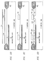
- Figure 1 is a sectional view of a sample CMOS structure according to the disclosed inventions.
- a p-type substrate 102 contains areas of thick field oxide 110 (e.g. 4000-5000 ⁇ thick) which define active device areas 114 therebetween. At least some areas of the field oxide 110 optionally overlie a conventional channel stop implant 112, but this is not necessarily present in all embodiments.
- thick field oxide 110 e.g. 4000-5000 ⁇ thick
- the active device regions include first portions 114A , which the surface monocrystalline portion overlies a buried oxide layer 120 , and second portions 114B in which the surface monocrystalline portion does not overlie the buried oxide layer 120 .
- the first active portions 114A include PMOS devices, of which a representative one is shown.
- the illustrated PMOS device includes a P+ source diffusion 130S and a P+ drain diffusion 130D , separated by an N- channel region 130C . Note that all of these regions overlie the buried oxide layer 120,
- the second active portions 114B include NMOS devices, of which a representative one is shown.
- the illustrated NMOS device includes an N+ source diffusion 132S and an N+ drain diffusion 132D , separated by a P- channel region 132C . Note that all of these regions overlie the p-type substrate 102.
- the PMOS and NMOS devices both have insulated gates which (in this embodiment) are formed from a thin-film polysilicon layer 140 . (Alternatively, of course, this could be a polycide layer, or the PMOS and NMOS gates can be formed from separate thin-film layers.)
- a passivation layer 150 overlies the transistor structures, except where patterned contact holes permit a patterned thin-film metal layer 160 to contact the polysilicon 140 or the active area 114.
- the layer 160 can also be polysilicon or silicide, with additional patterned conductor layers being formed in metal.
- CMOS output-nodes including the two data storage nodes of an SRAM cell.
- Figures 2A-2E show sequential steps in fabricating the structure of Figure 1.
- a p-type silicon substrate 102 is cleaned up, and a hardmask is formed and patterned.
- the hardmask covers area 102B and exposes area 102A .
- the hardmask itself may be, e.g. , 3000 ⁇ of low-temperature plasma oxide (or alternatively aluminum) over 2000 ⁇ of polyimide. (Of course a photoresist layer is also used to pattern the hardmask.)
- an optional screen oxide can then be grown (or deposited) over the silicon surface, e.g. to 500 ⁇ thickness, to reduce the depth of the buried oxide layer.
- the depth of the buried oxide layer is comparable to or less than the minimum achievable activated p+ source/drain junction depth, to minimize leakage.
- the buried oxide formation process is preferably adjusted to minimize the density of implantation-induced defects, as described in the literature cited above.
- An oxygen implant is then performed (e.g . with 1.8 ⁇ 10 18 cm -2 of oxygen ions at 190 keV).
- the hardmask is stripped ( e.g . by liftoff), and a high-temperature anneal is then performed, e.g . 360 minutes at 1320°C.
- the screen oxide layer (if any) can then be stripped.
- the implant energy and the thickness of the sacrificial surface oxide layer are selected to provide a thickness, in region 114A over buried oxide 120, of e.g . 1000 ⁇ . (Alternatively this thickness can be anywhere in the range from 200-3000 ⁇ ; smaller thicknesses tend to reduce topology, and are hence preferable.) Note that the silicon surface on the left side (area 102A) shows a slight volumetric expansion.
- a LOCOS stack is now formed and patterned to cover active device areas 114.
- a channel stop implant is now optionally performed, e.g . 10 13 -10 14 cm -2 of boron at 50 keV.
- Field oxide 110 is then grown ( e.g . to 5000 ⁇ thickness). Note, however, that thickness of the field oxide 110 must be sufficient to extend down to the buried oxide 120, in order to provide dielectric isolation around the source regions.
- the LOCOS stack is then stripped.
- a masked implant into regions 114A is now performed, to turn the crystalline silicon in this area n-type (lightly doped).
- this implant is 10 13 -10 14 cm -2 of phosphorus at 35 keV. (This implant may be performed using multiple steps at different energies, to obtain the desired vertical dopant profile.) Note that this implant is not required to be wholly coincident with the PMOS active areas 114, so this implant can be used to create lateral diodes if desired.
- a masked or blanket VT implant can also optionally be performed at this point, to adjust the threshold voltage of the NMOS devices.
- a sacrificial oxide is now grown and stripped, a gate oxide is grown, and a polysilicon layer 140 is deposited and patterned. These steps result in the structure of Figure 2C .
- a masked N+ implant is used to form the N+ sources 132S and drains 132D
- a masked P+ implant is used to form the P+ sources 130S and drains 130D.
- an interlevel dielectric 150 is deposited, e.g. 3000 ⁇ of BPSG over 800 ⁇ of TEOS-deposited undoped oxide.
- the dielectric 150 is then patterned and etched to form contact holes 152, and thereafter can optionally be reflowed. These steps result in the structure of Figure 2E .
- a thin-film metal layer is deposited, patterned and etched to form the structure of Figure 1. Processing concludes with conventional steps, such as deposition and patterning a further interlevel dielectric, second metal, and protective overcoat.
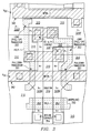
- Figure 3 shows a layout of a sample zero-power 6T SRAM cell.
- Two NMOS pull-down transistors 301 are loaded by two PMOS pull-up transistors 302.
- the active areas are separated by field oxide (isolation) areas 310.
- Masked p and n implants dope the active areas to form (where poly-1 is not present) p+ source/drain regions 320P and n+ source/drain regions 320N.
- the sources of PMOS transistors 302 are supplied by positive supply voltage V DD which is routed through metal line 340, and the sources of NMOS transistors 301 are supplied by ground voltage V SS which is routed through metal line 342.
- the drains of PMOS transistors 302 are ohmically connected to the drains of NMOS transistors 301 at merged contact locations 330.
- Each of these merged contact locations 330 corresponds to one of the data nodes of the cell, and is accessible through a pass transistor 352 (gated by word line 350 to provide connections to bitline contacts 354).
- a short metal jumper connects each of these merged contact locations 330 to the polysilicon gate lines of the transistors which drive the merged contact at the opposite node of the cell.
- FIG. 4 shows a sample zero-power SRAM memory.
- the illustrated example is the M48Z256/256Y memory, which is commercially available from SGS-Thomson, but of course the disclosed cell architecture can be used in other modules and chips too, and the specific illustrated module and chip architecture does not delimit the claimed inventions.
- the M48Z256/256Y x 8 ZEROPOWER RAM is a non-volatile 2,097,152 bit Static Ram organized as 262,144 words by 8 bits.
- the device combines two internal lithium batteries and full CMOS SRAMs in a plastic 32 pin DIP long Module.
- the ZEROPOWER RAM directly replaces industry standard SRAMs. It also fits into many EPROM and EEPROM sockets, providing the nonvolatility of PROMs without any requirement for special write timing or limitations on the number or writes that can be performed.
- the M48Z256/256Y has its own Power-fail Defect Circuit.
- the control circuitry constantly monitors the single 5V supply for an out of tolerance condition. When V CC is out of tolerance, the circuit wire protects the SRAM, providing a high degree of data security in the midst of unpredictable system operations brought on by low V CC . As V CC falls below approximately 3V, the control circuitry connects the batteries which sustain data until valid power returns.
- the M48Z256/256Y is in the Read Mode whenever W(White Enable) is high and E(Chip Enable) is low.
- the device architecture allows ripple-through access of data from eight of 2,097,152 locations in the state storage array.
- the unique address specified by the 18 Address Inputs defines which one of the 262,144 bytes of data is to be accessed.
- Valid data will be available at the Data I/O pins within t AVOV (Address Access Time) after the last address input signal is stable, providing that the E ⁇ and G ⁇ (Output Enable) access times are also satisfied. If the E ⁇ and G ⁇ access times are not met, valid data will be available after the later of Chip Enable Access Time (t ELOV ) or Output Enable Access Time (t GLOV ).
- the state of the eight three-state Data I/O signals is controlled by E ⁇ and G ⁇ . If the outputs are activated before t AVOV , the data lines will be driven to an indeterminate state until t AVOV . If the Address Inputs are changed while E ⁇ and G ⁇ remain low, output data will remain valid for t AXOX (Output Data Hold Time) but will go indeterminate until the next Address Access.
- the M48Z256/256Y is in the Write Mode whenever W and E are active.
- the start of a write is referenced from the latter occurring falling edge of W ⁇ or E ⁇ .
- a write is terminated by the earlier rising edge of W ⁇ or E ⁇ .
- An integrated circuit device structure comprising: a first field-effect transistor, having source and drain diffusions of a first conductivity type located in and defining a channel region therebetween in a first monocrystalline semiconductor region; and a second field-effect transistor, having source and drain diffusions of a second conductivity type located in and defining a channel region therebetween in a second monocrystalline semiconductor region; wherein said first and second regions are both lattice-matched to an underlying monocrystalline semiconductor substrate; and wherein said second region, but not said first region, is separated from said substrate by a buried dielectric layer having a compositional profile characteristic of implantation of an oxidizing species followed by annealing.
- An integrated circuit inverter structure comprising: a first field-effect transistor, having source and drain diffusions of a first conductivity type located in and defining a channel region therebetween in a first monocrystalline semiconductor region; and a second field-effect transistor, having source and drain diffusions of a second conductivity type located in and defining a channel region therebetween in a second monocrystalline semiconductor region; wherein said first and second regions are both lattice-matched to an underlying monocrystalline semiconductor substrate; and wherein said second region, but not said first region, is separated from said substrate by a buried dielectric layer; and wherein said first and second transistors have respective insulated gates which are connected together, and have said respective drain diffusions connected together at a shared contact location.
- An integrated circuit latch structure comprising: first and third field-effect transistors, having source and drain diffusions of a first conductivity type located in and defining a channel region therebetween in a first monocrystalline semiconductor region; and second and fourth field-effect transistors, having source and drain diffusions of a second conductivity type located in and defining a channel region therebetween in a second monocrystalline semiconductor region; wherein said first and second regions are both lattice-matched to an underlying monocrystalline semiconductor substrate, and said second region, but not said first region, is separated from said substrate by a buried dielectric layer; and wherein said first and second transistors have said respective drain diffusions connected together at a shared contact location, and are interconnected with said third and fourth transistors to form a latch.
- An integrated circuit SRAM cell structure comprising: first and third field-effect transistors, having source and drain diffusions of a first conductivity type located in and defining a channel region therebetween in a first monocrystalline semiconductor region; and second and fourth field-effect transistors, having source and drain diffusions of a second conductivity type located in and defining a channel region therebetween in a second monocrystalline semiconductor region; wherein said first and second regions are both lattice-matched to an underlying monocrystalline semiconductor substrate, and said second region, but not said first region, is separated from said substrate by a buried dielectric layer; and wherein said first and second transistors have said respective drain diffusions connected together at a shared contact location, and are interconnected with said third and fourth transistors to form a latch; and further comprising an additional transistor which is connected to provide selectable access to said shared contact location.
- An SRAM memory comprising: an array of memory cells arranged in rows and columns; address decoding circuitry, connected to receive address signals and accordingly provide decoded address outputs; and row and column selection circuitry, connected to access ones of said cells in accordance with said decoded address outputs; wherein multiple individual ones of said cells each comprise two first-conductivity-type field-effect transistors having source and drain diffusions located in and defining a channel region therebetween in a first monocrystalline semiconductor region; and two second-conductivity-type field-effect transistors having source and drain diffusions located in and defining a channel region therebetween in a second monocrystalline semiconductor region; wherein said first and second regions are both lattice-matched to an underlying monocrystalline semiconductor substrate, and wherein said second region, but not said first region, is separated from said substrate by a buried dielectric layer; said transistors being interconnected to form a latch.
- An integrated circuit fabrication method comprising the steps of: providing substantially monolithic semiconductor material; selectively forming a buried dielectric layer which underlies first, but not second, monocrystalline portions of said semiconductor material; forming field effect transistors of a first conductivity type in said first monocrystalline portions; and forming field effect transistors of a second conductivity type in said second monocrystalline portions.
- An integrated circuit fabrication method comprising the steps of: providing substantially monolithic semiconductor material; masking a portion of said semiconductor material, and implanting an unmasked portion of said semiconductor material with an oxidizing species at a dose greater than 10 17 cm -2 ; annealing said semiconductor material under conditions which cause said oxidizing species to react with said semiconductor material to thereby form a buried dielectric layer; forming field dielectric regions to separate portions of said semiconductor material, wherein said field dielectric regions define active areas of said semiconductor material therebetween; said field dielectric regions extending down into said semiconductor material at least to the depth of said buried dielectric layer; forming first-conductivity-type transistors in ones of said active areas which overlie portions of said buried dielectric layer; and forming transistors of a second conductivity type in ones of said active areas which do not overlie portions of said buried dielectric layer.
- An integrated circuit fabrication method comprising the steps of: providing substantially monolithic semiconductor material; masking a portion of said semiconductor material, and implanting an unmasked portion of said semiconductor material with an oxidizing species at a dose greater than 10 17 cm -2 ; annealing said semiconductor material under conditions which cause said oxidizing species to react with said semiconductor material to thereby form a buried dielectric layer; forming field dielectric regions to separate portions of said semiconductor material, wherein said field dielectric regions define active areas of said semiconductor material therebetween; said field dielectric regions extending down into said semiconductor material at least to the depth of said buried dielectric layer; forming first transistors, which have respective source and drain regions of a first conductivity type, in ones of said active areas which overlie portions of said buried dielectric layer; and forming second transistors, which have respective source and drain regions of a second conductivity type, in ones of said active areas which do not overlie portions of said buried dielectric layer; wherein at least some drain regions of said
- the first conductivity may be N-type.
- the semiconductor material may be silicon.
- All the transistors may be insualted gate field-effect transistors.
- the semiconductor material may be silicon, and the buried dielectric may be a buried layer of silicon oxide.
Abstract
Description
- The present inventions relate to integrated circuit devices and processes, and particularly to CMOS devices and processes which are highly resistant to latchup.
- One of the important limitations to the scaling down of Complementary MOS (CMOS) devices is the design rule for the NMOS-to-PMOS spacing. While all other circuit design rules for the current technology are well below 1 µm, the design rule for NMOS-to-PMOS spacing is still typically in the neighborhood of 2-3 micrometers. This rule originates from the need of separate deep implantation of the n- and p-type dopants followed by a drive-in. The lateral distribution of the dopant makes the transition region between the n-well and the p-well very wide, and no active devices can be built there. For that reason, placing small and repetitive elements of CMOS circuitry such as memory cells next to each other requires a large amount of area, and is usually avoided if possible. However, such placement may become indispensable for certain applications such as zero-power SRAM devices.
- Latchup considerations also place some limitations on n+ to p+ spacing in bulk CMOS technologies. Latchup is one of the basic problems of CMOS technology. Consider the sequence of a PMOS source region, the surrounding N-well region, a p-well region (or p-type epitaxial layer), and an NMOS source region. This sequence of regions will inevitably occur in normal bulk CMOS designs, and it defines a thyristor. This thyristor is referred to as "parasitic," since it is not created intentionally. A thyristor is a bipolar device which has an extremely low on-resistance. Once the thyristor turns on (or "fires"), it will remain on for as long as it can draw its minimum holding current. This behavior is extremely undesirable in integrated circuits, since when such a parasitic thyristor fires it may destroy the integrated circuit (by drawing excessive current), or may rapidly discharge a portable system's battery, or may simply cause the chip to remain in a "stuck" condition, and hence become unusable, until the power supply is disconnected.
- An SRAM cell consists typically of two n-channel pass transistors (which selectably connect the cell latch to a pair of bit-lines), two cross-coupled n-channel driver transistors, and two more active or passive devices acting as the load (or pull-up) devices. Ordinarily, the parameters of these pull-ups are non-critical, and they can be made of material with relatively poor electrical properties, such as polysilicon. In this case the pull-ups can be stacked on top of the n-channel MOSFETs (which have their channels in the monocrystalline substrate). This ensures that the cell area is kept to a minimum, while the n-MOSFETs still have the necessary quality. One of the drawbacks of this approach is the relatively high leakage current of the cell and its high temperature coefficient; but this is not a critical drawback in commodity SRAM specifications.
- In "zero-power" applications the information in an SRAM cell must be retained for an extended period (e.g. 10 years) while sustained only by a small battery. For such applications it is important that the leakage of the SRAM cell be minimal. Thus, such applications usually form the PMOS pull-up devices in the substrate, but this means the NMOS-to-PMOS spacing rules degrade density. For this reason the density of zero-power SRAM cells is only about half that of mainstream commodity SRAMs.
- One possible way to bypass the need for wells is to build one of the device types as an SOI (silicon-on-insulator) structure. This avoids the need for NMOS-to-PMOS design rules. One such architecture is described in commonly-owned prior application 08/397,654 filed 2/28/95 (and now pending), which is hereby incorporated by reference.
- The present application is intended to provide improvements over the approach described in the 08/397,654 application, including improved topography, avoidance of the need for selective epitaxy and/or recrystallization of polysilicon, and avoidance of excessive oxide growth steps.
- The present application discloses a memory cell process in which a patterned buried oxide layer is formed under the PMOS devices by a high-dose high-energy oxygen implant. A hardmask screens this implant from the NMOS device areas. After a high-temperature anneal, the patterned oxygen implant provides a buried oxide layer. This provides dielectric isolation under the PMOS devices, and thus:
avoids NMOS-to-PMOS spacing rules;
reduces leakage as compared to thin-film transistors; and
makes latchup impossible. - The disclosed inventions will be described with reference to the accompanying drawings, which show important sample embodiments of the invention and which are incorporated in the specification hereof by reference, wherein:
- Figure 1 is a sectional view of a sample CMOS structure according to the disclosed inventions.
- Figures 2A-2E show sequential steps in fabricating the structure of Figure 1.
- Figure 3 shows a layout of a sample zero-power 6T SRAM cell.
- Figure 4 shows a sample zero-power SRAM memory.
- The numerous innovative teachings of the present application will be described with particular reference to the presently preferred embodiment (by way of example, and not of limitation), in which:
- Figure 1 is a sectional view of a sample CMOS structure according to the disclosed inventions.
- A p-
type substrate 102 contains areas of thick field oxide 110 (e.g. 4000-5000Å thick) which defineactive device areas 114 therebetween. At least some areas of thefield oxide 110 optionally overlie a conventionalchannel stop implant 112, but this is not necessarily present in all embodiments. - The active device regions include
first portions 114A, which the surface monocrystalline portion overlies a buriedoxide layer 120, andsecond portions 114B in which the surface monocrystalline portion does not overlie the buriedoxide layer 120. - The first
active portions 114A include PMOS devices, of which a representative one is shown. The illustrated PMOS device includes aP+ source diffusion 130S and aP+ drain diffusion 130D, separated by an N-channel region 130C. Note that all of these regions overlie the buriedoxide layer 120, - The second
active portions 114B include NMOS devices, of which a representative one is shown. The illustrated NMOS device includes anN+ source diffusion 132S and anN+ drain diffusion 132D, separated by a P-channel region 132C. Note that all of these regions overlie the p-type substrate 102. - The PMOS and NMOS devices both have insulated gates which (in this embodiment) are formed from a thin-
film polysilicon layer 140. (Alternatively, of course, this could be a polycide layer, or the PMOS and NMOS gates can be formed from separate thin-film layers.) - A
passivation layer 150 overlies the transistor structures, except where patterned contact holes permit a patterned thin-film metal layer 160 to contact thepolysilicon 140 or theactive area 114. (Alternatively thelayer 160 can also be polysilicon or silicide, with additional patterned conductor layers being formed in metal.) - Note that in the structure shown the two
drain regions metal layer 160 makes contact to both drain regions. This is convenient for CMOS output-nodes, including the two data storage nodes of an SRAM cell. - Figures 2A-2E show sequential steps in fabricating the structure of Figure 1.
- Initially a p-
type silicon substrate 102 is cleaned up, and a hardmask is formed and patterned. The hardmask coversarea 102B and exposesarea 102A. The hardmask itself may be, e.g., 3000Å of low-temperature plasma oxide (or alternatively aluminum) over 2000Å of polyimide. (Of course a photoresist layer is also used to pattern the hardmask.) - At this point an optional screen oxide can then be grown (or deposited) over the silicon surface, e.g. to 500Å thickness, to reduce the depth of the buried oxide layer. Preferably the depth of the buried oxide layer is comparable to or less than the minimum achievable activated p+ source/drain junction depth, to minimize leakage. Similarly, the buried oxide formation process is preferably adjusted to minimize the density of implantation-induced defects, as described in the literature cited above.
- An oxygen implant is then performed (e.g. with 1.8×1018 cm-2 of oxygen ions at 190 keV).
- After implantation the hardmask is stripped (e.g. by liftoff), and a high-temperature anneal is then performed, e.g. 360 minutes at 1320°C. This produces the buried
oxide layer 120 shown on the left side of Figure 2A. The screen oxide layer (if any) can then be stripped. The implant energy and the thickness of the sacrificial surface oxide layer are selected to provide a thickness, inregion 114A over buriedoxide 120, of e.g. 1000Å. (Alternatively this thickness can be anywhere in the range from 200-3000Å; smaller thicknesses tend to reduce topology, and are hence preferable.) Note that the silicon surface on the left side (area 102A) shows a slight volumetric expansion. These steps result in the structure of Figure 2A. - A LOCOS stack is now formed and patterned to cover
active device areas 114. A channel stop implant is now optionally performed, e.g. 1013-1014 cm-2 of boron at 50 keV.Field oxide 110 is then grown (e.g. to 5000Å thickness). Note, however, that thickness of thefield oxide 110 must be sufficient to extend down to the buriedoxide 120, in order to provide dielectric isolation around the source regions. The LOCOS stack is then stripped. - A masked implant into
regions 114A is now performed, to turn the crystalline silicon in this area n-type (lightly doped). In a sample embodiment, this implant is 1013-1014 cm-2 of phosphorus at 35 keV. (This implant may be performed using multiple steps at different energies, to obtain the desired vertical dopant profile.) Note that this implant is not required to be wholly coincident with the PMOSactive areas 114, so this implant can be used to create lateral diodes if desired. - A masked or blanket VT implant can also optionally be performed at this point, to adjust the threshold voltage of the NMOS devices.
- These steps result in the structure of Figure 2B. Note that one
part 114A of theactive area 114 overlies the buriedoxide 120, while anotherpart 114B does not. - A sacrificial oxide is now grown and stripped, a gate oxide is grown, and a
polysilicon layer 140 is deposited and patterned. These steps result in the structure of Figure 2C. - Thereafter, a masked N+ implant is used to form the
N+ sources 132S and drains 132D, and a masked P+ implant is used to form theP+ sources 130S and drains 130D. (These are self-aligned to thegate layer 140, or may optionally be self-aligned to optional sidewall spacers on thegate layer 140.) These steps result in the structure of Figure 2D. - Thereafter an
interlevel dielectric 150 is deposited, e.g. 3000Å of BPSG over 800Å of TEOS-deposited undoped oxide. The dielectric 150 is then patterned and etched to form contact holes 152, and thereafter can optionally be reflowed. These steps result in the structure of Figure 2E. - Thereafter, a thin-film metal layer is deposited, patterned and etched to form the structure of Figure 1. Processing concludes with conventional steps, such as deposition and patterning a further interlevel dielectric, second metal, and protective overcoat.
- Figure 3 shows a layout of a sample zero-power 6T SRAM cell. Two NMOS pull-down
transistors 301 are loaded by two PMOS pull-uptransistors 302. The active areas are separated by field oxide (isolation)areas 310. Masked p and n implants dope the active areas to form (where poly-1 is not present) p+ source/drain regions 320P and n+ source/drain regions 320N. The sources ofPMOS transistors 302 are supplied by positive supply voltage VDD which is routed throughmetal line 340, and the sources ofNMOS transistors 301 are supplied by ground voltage VSS which is routed throughmetal line 342. The drains ofPMOS transistors 302 are ohmically connected to the drains ofNMOS transistors 301 atmerged contact locations 330. Each of thesemerged contact locations 330 corresponds to one of the data nodes of the cell, and is accessible through a pass transistor 352 (gated byword line 350 to provide connections to bitline contacts 354). Note that a short metal jumper connects each of thesemerged contact locations 330 to the polysilicon gate lines of the transistors which drive the merged contact at the opposite node of the cell. - Figure 4 shows a sample zero-power SRAM memory. The illustrated example is the M48Z256/256Y memory, which is commercially available from SGS-Thomson, but of course the disclosed cell architecture can be used in other modules and chips too, and the specific illustrated module and chip architecture does not delimit the claimed inventions.
- Notable features of this module include:
- It is an integrated module which combines low power SRAMs, power-fail control circuit, and batteries.
- It provides conventional SRAM operation, with unlimited write cycles.
- It provides 10 years of data retention in the absence of power.
- It provides pin and function compatible with jedec standard 256k x 8 SRAMs.
- It provides automatic power-fail chip deselect and write protection.
- It provides a choice of two write protect voltages:
in version M48Z256: 4.5V ≦ VPFD ≦ 4.75V; or
in version M48Z256Y: 4.2V ≦ VPFD ≦ 4.50V. - Its batteries are internally isolated until power is applied.
- The M48Z256/256Y x 8 ZEROPOWER RAM is a non-volatile 2,097,152 bit Static Ram organized as 262,144 words by 8 bits. The device combines two internal lithium batteries and full CMOS SRAMs in a plastic 32 pin DIP long Module.
- The ZEROPOWER RAM directly replaces industry standard SRAMs. It also fits into many EPROM and EEPROM sockets, providing the nonvolatility of PROMs without any requirement for special write timing or limitations on the number or writes that can be performed.
- The M48Z256/256Y has its own Power-fail Defect Circuit. The control circuitry constantly monitors the single 5V supply for an out of tolerance condition. When VCC is out of tolerance, the circuit wire protects the SRAM, providing a high degree of data security in the midst of unpredictable system operations brought on by low VCC. As VCC falls below approximately 3V, the control circuitry connects the batteries which sustain data until valid power returns.
- The M48Z256/256Y is in the Read Mode whenever W(White Enable) is high and E(Chip Enable) is low. The device architecture allows ripple-through access of data from eight of 2,097,152 locations in the state storage array. Thus, the unique address specified by the 18 Address Inputs defines which one of the 262,144 bytes of data is to be accessed. Valid data will be available at the Data I/O pins within tAVOV (Address Access Time) after the last address input signal is stable, providing that the E\ and G\ (Output Enable) access times are also satisfied. If the E\ and G\ access times are not met, valid data will be available after the later of Chip Enable Access Time (tELOV) or Output Enable Access Time (tGLOV).
- The state of the eight three-state Data I/O signals is controlled by E\ and G\. If the outputs are activated before tAVOV, the data lines will be driven to an indeterminate state until tAVOV. If the Address Inputs are changed while E\ and G\ remain low, output data will remain valid for tAXOX (Output Data Hold Time) but will go indeterminate until the next Address Access.
- The M48Z256/256Y is in the Write Mode whenever W and E are active. The start of a write is referenced from the latter occurring falling edge of W\ or E\. A write is terminated by the earlier rising edge of W\ or E\.
- According to a disclosed class of innovative embodiments, there is provided: An integrated circuit device structure, comprising: a first field-effect transistor, having source and drain diffusions of a first conductivity type located in and defining a channel region therebetween in a first monocrystalline semiconductor region; and a second field-effect transistor, having source and drain diffusions of a second conductivity type located in and defining a channel region therebetween in a second monocrystalline semiconductor region; wherein said first and second regions are both lattice-matched to an underlying monocrystalline semiconductor substrate; and wherein said second region, but not said first region, is separated from said substrate by a buried dielectric layer having a compositional profile characteristic of implantation of an oxidizing species followed by annealing.
- According to another disclosed class of innovative embodiments, there is provided: An integrated circuit inverter structure, comprising: a first field-effect transistor, having source and drain diffusions of a first conductivity type located in and defining a channel region therebetween in a first monocrystalline semiconductor region; and a second field-effect transistor, having source and drain diffusions of a second conductivity type located in and defining a channel region therebetween in a second monocrystalline semiconductor region; wherein said first and second regions are both lattice-matched to an underlying monocrystalline semiconductor substrate; and wherein said second region, but not said first region, is separated from said substrate by a buried dielectric layer; and wherein said first and second transistors have respective insulated gates which are connected together, and have said respective drain diffusions connected together at a shared contact location.
- According to another disclosed class of innovative embodiments, there is provided: An integrated circuit latch structure, comprising: first and third field-effect transistors, having source and drain diffusions of a first conductivity type located in and defining a channel region therebetween in a first monocrystalline semiconductor region; and second and fourth field-effect transistors, having source and drain diffusions of a second conductivity type located in and defining a channel region therebetween in a second monocrystalline semiconductor region; wherein said first and second regions are both lattice-matched to an underlying monocrystalline semiconductor substrate, and said second region, but not said first region, is separated from said substrate by a buried dielectric layer; and wherein said first and second transistors have said respective drain diffusions connected together at a shared contact location, and are interconnected with said third and fourth transistors to form a latch.
- According to another disclosed class of innovative embodiments, there is provided: An integrated circuit SRAM cell structure, comprising: first and third field-effect transistors, having source and drain diffusions of a first conductivity type located in and defining a channel region therebetween in a first monocrystalline semiconductor region; and second and fourth field-effect transistors, having source and drain diffusions of a second conductivity type located in and defining a channel region therebetween in a second monocrystalline semiconductor region; wherein said first and second regions are both lattice-matched to an underlying monocrystalline semiconductor substrate, and said second region, but not said first region, is separated from said substrate by a buried dielectric layer; and wherein said first and second transistors have said respective drain diffusions connected together at a shared contact location, and are interconnected with said third and fourth transistors to form a latch; and further comprising an additional transistor which is connected to provide selectable access to said shared contact location.
- According to another disclosed class of innovative embodiments, there is provided: An SRAM memory, comprising: an array of memory cells arranged in rows and columns; address decoding circuitry, connected to receive address signals and accordingly provide decoded address outputs; and row and column selection circuitry, connected to access ones of said cells in accordance with said decoded address outputs; wherein multiple individual ones of said cells each comprise two first-conductivity-type field-effect transistors having source and drain diffusions located in and defining a channel region therebetween in a first monocrystalline semiconductor region; and two second-conductivity-type field-effect transistors having source and drain diffusions located in and defining a channel region therebetween in a second monocrystalline semiconductor region; wherein said first and second regions are both lattice-matched to an underlying monocrystalline semiconductor substrate, and wherein said second region, but not said first region, is separated from said substrate by a buried dielectric layer; said transistors being interconnected to form a latch.
- According to another disclosed class of innovative embodiments, there is provided: An integrated circuit fabrication method, comprising the steps of: providing substantially monolithic semiconductor material; selectively forming a buried dielectric layer which underlies first, but not second, monocrystalline portions of said semiconductor material; forming field effect transistors of a first conductivity type in said first monocrystalline portions; and forming field effect transistors of a second conductivity type in said second monocrystalline portions.
- According to another disclosed class of innovative embodiments, there is provided: An integrated circuit fabrication method, comprising the steps of: providing substantially monolithic semiconductor material; masking a portion of said semiconductor material, and implanting an unmasked portion of said semiconductor material with an oxidizing species at a dose greater than 1017 cm-2; annealing said semiconductor material under conditions which cause said oxidizing species to react with said semiconductor material to thereby form a buried dielectric layer; forming field dielectric regions to separate portions of said semiconductor material, wherein said field dielectric regions define active areas of said semiconductor material therebetween; said field dielectric regions extending down into said semiconductor material at least to the depth of said buried dielectric layer; forming first-conductivity-type transistors in ones of said active areas which overlie portions of said buried dielectric layer; and forming transistors of a second conductivity type in ones of said active areas which do not overlie portions of said buried dielectric layer.
- According to another disclosed class of innovative embodiments, there is provided: An integrated circuit fabrication method, comprising the steps of: providing substantially monolithic semiconductor material; masking a portion of said semiconductor material, and implanting an unmasked portion of said semiconductor material with an oxidizing species at a dose greater than 1017 cm-2; annealing said semiconductor material under conditions which cause said oxidizing species to react with said semiconductor material to thereby form a buried dielectric layer; forming field dielectric regions to separate portions of said semiconductor material, wherein said field dielectric regions define active areas of said semiconductor material therebetween; said field dielectric regions extending down into said semiconductor material at least to the depth of said buried dielectric layer; forming first transistors, which have respective source and drain regions of a first conductivity type, in ones of said active areas which overlie portions of said buried dielectric layer; and forming second transistors, which have respective source and drain regions of a second conductivity type, in ones of said active areas which do not overlie portions of said buried dielectric layer; wherein at least some drain regions of said second transistors abut drain region regions of said first transistors at ohmic contact locations.
- As will be recognized by those skilled in the art, the innovative concepts described in the present application can be modified and varied over a tremendous range of applications, and accordingly the scope of patented subject matter is not limited by any of the specific exemplary teachings given. For example, as will be obvious to those of ordinary skill in the art, other circuit elements can be added to, or substituted into, the specific circuit topologies shown.
- The first conductivity may be N-type.
- The semiconductor material may be silicon.
- All the transistors may be insualted gate field-effect transistors.
- The semiconductor material may be silicon, and the buried dielectric may be a buried layer of silicon oxide.
Claims (18)
- An integrated circuit device structure, comprising:a first field-effect transistor, having source and drain diffusions of a first conductivity type located in and defining a channel region therebetween in a first monocrystalline semiconductor region; anda second field-effect transistor, having source and drain diffusions of a second conductivity type located in and defining a channel region therebetween in a second monocrystalline semiconductor region;
wherein said first and second regions are both lattice-matched to an underlying monocrystalline semiconductor substrate;
and wherein said second region, but not said first region, is separated from said substrate by a buried dielectric layer having a compositional profile characteristic of implantation of an oxidizing species followed by annealing. - An integrated circuit inverter structure, comprising:a first field-effect transistor, having source and drain diffusions of a first conductivity type located in and defining a channel region therebetween in a first monocrystalline semiconductor region; anda second field-effect transistor, having source and drain diffusions of a second conductivity type located in and defining a channel region therebetween in a second monocrystalline semiconductor region;
wherein said first and second regions are both lattice-matched to an underlying monocrystalline semiconductor substrate;
and wherein said second region, but not said first region, is separated from said substrate by a buried dielectric layer;
and wherein said first and second transistors have respective insulated gates which are connected together, and have said respective drain diffusions connected together at a shared contact location. - An integrated circuit latch structure, comprising:first and third field-effect transistors, having source and drain diffusions of a first conductivity type located in and defining a channel region therebetween in a first monocrystalline semiconductor region; andsecond and fourth field-effect transistors, having source and drain diffusions of a second conductivity type located in and defining a channel region therebetween in a second monocrystalline semiconductor region;
wherein said first and second regions are both lattice-matched to an underlying monocrystalline semiconductor substrate, and said second region, but not said first region, is separated from said substrate by a buried dielectric layer;
and wherein said first and second transistors have said respective drain diffusions connected together at a shared contact location, and are interconnected with said third and fourth transistors to form a latch. - An integrated circuit SRAM cell structure, comprising:first and third field-effect transistors, having source and drain diffusions of a first conductivity type located in and defining a channel region therebetween in a first monocrystalline semiconductor region; andsecond and fourth field-effect transistors, having source and drain diffusions of a second conductivity type located in and defining a channel region therebetween in a second monocrystalline semiconductor region;
wherein said first and second regions are both lattice-matched to an underlying monocrystalline semiconductor substrate, and said second region, but not said first region, is separated from said substrate by a buried dielectric layer;
and wherein said first and second transistors have said respective drain diffusions connected together at a shared contact location, and are interconnected with said third and fourth transistors to form a latch; and further comprising
an additional transistor which is connected to provide selectable access to said shared contact location. - The integrated circuit structure of any one of claims 1 to 4 wherein said third and first transistors are NMOS, and said second and fourth transistors are PMOS.
- An SRAM memory, comprising:an array of memory cells arranged in rows and columns;address decoding circuitry, connected to receive address signals and accordingly provide decoded address outputs; androw and column selection circuitry, connected to access ones of said cells in accordance with said decoded address outputs;
wherein multiple individual ones of said cells each comprisetwo first-conductivity-type field-effect transistors having source and drain diffusions located in and defining a channel region therebetween in a first monocrystalline semiconductor region; andtwo second-conductivity-type field-effect transistors having source and drain diffusions located in and defining a channel region therebetween in a second monocrystalline semiconductor region; wherein said first and second regions are both lattice-matched to an underlying monocrystalline semiconductor substrate, and wherein said second region, but not said first region, is separated from said substrate by a buried dielectric layer;
said transistors being interconnected to form a latch. - The integrated circuit structure of any one of claims 1 to 4 or the memory of claim 6 wherein said buried dielectric layer has a compositional profile characteristic of implantation of an oxidizing species followed by annealing.
- The memory of claim 6, wherein said second-conductivity-type transistors are PMOS.
- An integrated circuit fabrication method, comprising the steps of:(a) providing substantially monolithic semiconductor material;(b) selectively forming a buried dielectric layer which underlies first, but not second, monocrystalline portions of said semiconductor material;(c) forming field effect transistors of a first conductivity type in said first monocrystalline portions; and(d) forming field effect transistors of a second conductivity type in said second monocrystalline portions.
- The method of claim 9 wherein said buried dielectric layer is formed by implantation of an oxidizing species followed by annealing.
- The method of Claim 9, further comprising the additional step, after said step (b.), of forming field dielectric regions to separate portions of said semiconductor material, wherein said field dielectric regions define active areas of said semiconductor material therebetween; said field dielectric regions extending down into said semiconductor material at least to the depth of said buried dielectric layer;
- An integrated circuit fabrication method, comprising the steps of:(a.) providing substantially monolithic semiconductor material;(b.) masking a portion of said semiconductor material, and implanting an unmasked portion of said semiconductor material with an oxidizing species at a dose greater than 1017 cm-2;(c.) annealing said semiconductor material under conditions which cause said oxidizing species to react with said semiconductor material to thereby form a buried dielectric layer;(d.) forming field dielectric regions to separate portions of said semiconductor material, wherein said field dielectric regions define active areas of said semiconductor material therebetween; said field dielectric regions extending down into said semiconductor material at least to the depth of said buried dielectric layer;(e.) forming first-conductivity-type transistors in ones of said active areas which overlie portions of said buried dielectric layer; and(f.) forming transistors of a second conductivity type in ones of said active areas which do not overlie portions of said buried dielectric layer.
- The method of claim 12, wherein said masking step uses at least one patterned inorganic masking layer.
- An integrated circuit fabrication method, comprising the steps of:(a.) providing substantially monolithic semiconductor material;(b.) masking a portion of said semiconductor material, and implanting an unmasked portion of said semiconductor material with an oxidizing species at a dose greater than 1017 cm-2;(c.) annealing said semiconductor material under conditions which cause said oxidizing species to react with said semiconductor material to thereby form a buried dielectric layer;(d.) forming field dielectric regions to separate portions of said semiconductor material, wherein said field dielectric regions define active areas of said semiconductor material therebetween; said field dielectric regions extending down into said semiconductor material at least to the depth of said buried dielectric layer;(e.) forming first transistors, which have respective source and drain regions of a first conductivity type, in ones of said active areas which overlie portions of said buried dielectric layer; and(f.) forming second transistors, which have respective source and drain regions of a second conductivity type, in ones of said active areas which do not overlie portions of said buried dielectric layer;
wherein at least some drain regions of said second transistors abut drain region regions of said first transistors at ohmic contact locations. - The integrated circuit structure of any one of claims 1 to 4, the memory of claim 6 or the method of any one of claims 9, 12 or 14 wherein said buried dielectric is a buried oxide.
- The integrated circuit structure of any one of claims 1 to 4, the memory of claim 6 or the method of any one of claims 9, 12 or 14 wherein said implanting step uses an ion energy of at least about 100keV.
- The integrated circuit structure of any one of claims 1 to 4, the memory of claim 6 or the method of any one of claims 9, 12 or 14 wherein said first and second regions adjoin with no intervening dielectric therebetween.
- A product formed by the process of any one of claims 9, 12 or 14.
Applications Claiming Priority (2)
| Application Number | Priority Date | Filing Date | Title |
|---|---|---|---|
| US47824795A | 1995-06-07 | 1995-06-07 | |
| US478247 | 1995-06-07 |
Publications (2)
| Publication Number | Publication Date |
|---|---|
| EP0747961A2 true EP0747961A2 (en) | 1996-12-11 |
| EP0747961A3 EP0747961A3 (en) | 1998-11-11 |
Family
ID=23899140
Family Applications (1)
| Application Number | Title | Priority Date | Filing Date |
|---|---|---|---|
| EP96303776A Withdrawn EP0747961A3 (en) | 1995-06-07 | 1996-05-28 | Zero-power SRAM with patterned buried oxide isolation |
Country Status (3)
| Country | Link |
|---|---|
| US (1) | US5795800B1 (en) |
| EP (1) | EP0747961A3 (en) |
| JP (1) | JPH0922951A (en) |
Cited By (19)
| Publication number | Priority date | Publication date | Assignee | Title |
|---|---|---|---|---|
| WO2000048245A1 (en) * | 1999-02-12 | 2000-08-17 | Ibis Technology Corporation | Patterned silicon-on-insulator devices |
| US6559470B2 (en) | 2000-06-22 | 2003-05-06 | Progressed Technologies, Inc. | Negative differential resistance field effect transistor (NDR-FET) and circuits using the same |
| US6567292B1 (en) | 2002-06-28 | 2003-05-20 | Progressant Technologies, Inc. | Negative differential resistance (NDR) element and memory with reduced soft error rate |
| US6594193B2 (en) | 2000-06-22 | 2003-07-15 | Progressent Technologies, Inc. | Charge pump for negative differential resistance transistor |
| US6724655B2 (en) | 2000-06-22 | 2004-04-20 | Progressant Technologies, Inc. | Memory cell using negative differential resistance field effect transistors |
| US6795337B2 (en) | 2002-06-28 | 2004-09-21 | Progressant Technologies, Inc. | Negative differential resistance (NDR) elements and memory device using the same |
| US6806117B2 (en) | 2002-12-09 | 2004-10-19 | Progressant Technologies, Inc. | Methods of testing/stressing a charge trapping device |
| US6812084B2 (en) | 2002-12-09 | 2004-11-02 | Progressant Technologies, Inc. | Adaptive negative differential resistance device |
| US6847562B2 (en) | 2002-06-28 | 2005-01-25 | Progressant Technologies, Inc. | Enhanced read and write methods for negative differential resistance (NDR) based memory device |
| US6849483B2 (en) | 2002-12-09 | 2005-02-01 | Progressant Technologies, Inc. | Charge trapping device and method of forming the same |
| US6853035B1 (en) | 2002-06-28 | 2005-02-08 | Synopsys, Inc. | Negative differential resistance (NDR) memory device with reduced soft error rate |
| US6864104B2 (en) | 2002-06-28 | 2005-03-08 | Progressant Technologies, Inc. | Silicon on insulator (SOI) negative differential resistance (NDR) based memory device with reduced body effects |
| US6894327B1 (en) | 2001-12-21 | 2005-05-17 | Progressant Technologies, Inc. | Negative differential resistance pull up element |
| US6912151B2 (en) | 2002-06-28 | 2005-06-28 | Synopsys, Inc. | Negative differential resistance (NDR) based memory device with reduced body effects |
| US6980467B2 (en) | 2002-12-09 | 2005-12-27 | Progressant Technologies, Inc. | Method of forming a negative differential resistance device |
| US6979580B2 (en) | 2002-12-09 | 2005-12-27 | Progressant Technologies, Inc. | Process for controlling performance characteristics of a negative differential resistance (NDR) device |
| US7005711B2 (en) | 2002-12-20 | 2006-02-28 | Progressant Technologies, Inc. | N-channel pull-up element and logic circuit |
| US7012833B2 (en) | 2002-12-09 | 2006-03-14 | Progressant Technologies, Inc. | Integrated circuit having negative differential resistance (NDR) devices with varied peak-to-valley ratios (PVRs) |
| US7453083B2 (en) | 2001-12-21 | 2008-11-18 | Synopsys, Inc. | Negative differential resistance field effect transistor for implementing a pull up element in a memory cell |
Families Citing this family (23)
| Publication number | Priority date | Publication date | Assignee | Title |
|---|---|---|---|---|
| JP3556679B2 (en) * | 1992-05-29 | 2004-08-18 | 株式会社半導体エネルギー研究所 | Electro-optical device |
| US5693975A (en) * | 1995-10-05 | 1997-12-02 | Integrated Device Technology, Inc. | Compact P-channel/N-channel transistor structure |
| US5877048A (en) * | 1998-03-23 | 1999-03-02 | Texas Instruments--Acer Incorporated | 3-D CMOS transistors with high ESD reliability |
| US6172899B1 (en) * | 1998-05-08 | 2001-01-09 | Micron Technology. Inc. | Static-random-access-memory cell |
| KR100292818B1 (en) * | 1998-07-02 | 2001-11-05 | 윤종용 | MOS transistor manufacturing method |
| US6342438B2 (en) * | 1998-11-06 | 2002-01-29 | Advanced Micro Devices, Inc. | Method of manufacturing a dual doped CMOS gate |
| US5994759A (en) * | 1998-11-06 | 1999-11-30 | National Semiconductor Corporation | Semiconductor-on-insulator structure with reduced parasitic capacitance |
| KR100548593B1 (en) * | 1998-12-31 | 2006-05-12 | 주식회사 하이닉스반도체 | SRAM cell structure |
| US6336868B1 (en) * | 1999-04-06 | 2002-01-08 | American Axle & Manufacturing, Inc. | Universal joint with thrust washer |
| US6232170B1 (en) * | 1999-06-16 | 2001-05-15 | International Business Machines Corporation | Method of fabricating trench for SOI merged logic DRAM |
| US6287901B1 (en) | 2000-01-05 | 2001-09-11 | International Business Machines Corporation | Method and semiconductor structure for implementing dual plane body contacts for silicon-on-insulator (SOI) transistors |
| US6461902B1 (en) * | 2000-07-18 | 2002-10-08 | Institute Of Microelectronics | RF LDMOS on partial SOI substrate |
| US6812529B2 (en) * | 2001-03-15 | 2004-11-02 | Micron Technology, Inc. | Suppression of cross diffusion and gate depletion |
| US6531375B1 (en) | 2001-09-18 | 2003-03-11 | International Business Machines Corporation | Method of forming a body contact using BOX modification |
| US6495429B1 (en) * | 2002-01-23 | 2002-12-17 | International Business Machines Corporation | Controlling internal thermal oxidation and eliminating deep divots in SIMOX by chlorine-based annealing |
| KR100422325B1 (en) * | 2002-06-12 | 2004-03-11 | 동부전자 주식회사 | Fabricating method of semiconductor device |
| JP3684232B2 (en) * | 2003-04-25 | 2005-08-17 | 株式会社東芝 | Semiconductor device |
| KR100539243B1 (en) | 2003-10-04 | 2005-12-27 | 삼성전자주식회사 | SRAM device on partial SOI substrate |
| US7187036B2 (en) * | 2004-03-31 | 2007-03-06 | Taiwan Semiconductor Manufacturing Company | Connection structure for SOI devices |
| DE102005063092B3 (en) * | 2005-12-30 | 2007-07-19 | Advanced Micro Devices, Inc., Sunnyvale | Semiconductor device having a contact structure with increased Ätzselektivität |
| US9349436B2 (en) | 2012-03-06 | 2016-05-24 | Taiwan Semiconductor Manufacturing Co., Ltd. | Semiconductor memory and method of making the same |
| US8947902B2 (en) | 2012-03-06 | 2015-02-03 | Taiwan Semiconductor Manufacturing Co., Ltd. | Semiconductor memory and method of making the same |
| WO2024077803A1 (en) * | 2022-10-13 | 2024-04-18 | 长鑫存储技术有限公司 | Semiconductor device and preparation method therefor |
Citations (4)
| Publication number | Priority date | Publication date | Assignee | Title |
|---|---|---|---|---|
| JPS63192266A (en) * | 1987-02-04 | 1988-08-09 | Oki Electric Ind Co Ltd | Cmos integrated circuit and manufacture thereof |
| US4810664A (en) * | 1986-08-14 | 1989-03-07 | Hewlett-Packard Company | Method for making patterned implanted buried oxide transistors and structures |
| US4829359A (en) * | 1987-05-29 | 1989-05-09 | Harris Corp. | CMOS device having reduced spacing between N and P channel |
| US5422296A (en) * | 1994-04-25 | 1995-06-06 | Motorola, Inc. | Process for forming a static-random-access memory cell |
Family Cites Families (4)
| Publication number | Priority date | Publication date | Assignee | Title |
|---|---|---|---|---|
| US4700454A (en) * | 1985-11-04 | 1987-10-20 | Intel Corporation | Process for forming MOS transistor with buried oxide regions for insulation |
| JPH04345064A (en) * | 1991-05-22 | 1992-12-01 | Hitachi Ltd | Semiconductor integrated circuit device and its manufacture |
| DE69316256T2 (en) * | 1992-03-26 | 1998-08-06 | Texas Instruments Inc | High voltage structure with oxide insulated source and RESURF drift zone in solid silicon |
| JP3060706B2 (en) * | 1992-04-01 | 2000-07-10 | 日産自動車株式会社 | Semiconductor device |
-
1996
- 1996-05-28 EP EP96303776A patent/EP0747961A3/en not_active Withdrawn
- 1996-05-28 JP JP8133479A patent/JPH0922951A/en active Pending
- 1996-07-25 US US08686395 patent/US5795800B1/en not_active Expired - Lifetime
Patent Citations (4)
| Publication number | Priority date | Publication date | Assignee | Title |
|---|---|---|---|---|
| US4810664A (en) * | 1986-08-14 | 1989-03-07 | Hewlett-Packard Company | Method for making patterned implanted buried oxide transistors and structures |
| JPS63192266A (en) * | 1987-02-04 | 1988-08-09 | Oki Electric Ind Co Ltd | Cmos integrated circuit and manufacture thereof |
| US4829359A (en) * | 1987-05-29 | 1989-05-09 | Harris Corp. | CMOS device having reduced spacing between N and P channel |
| US5422296A (en) * | 1994-04-25 | 1995-06-06 | Motorola, Inc. | Process for forming a static-random-access memory cell |
Non-Patent Citations (1)
| Title |
|---|
| PATENT ABSTRACTS OF JAPAN vol. 012, no. 474 (E-692), 12 December 1988 & JP 63 192266 A (OKI ELECTRIC IND CO LTD), 9 August 1988, * |
Cited By (33)
| Publication number | Priority date | Publication date | Assignee | Title |
|---|---|---|---|---|
| WO2000048245A1 (en) * | 1999-02-12 | 2000-08-17 | Ibis Technology Corporation | Patterned silicon-on-insulator devices |
| US6724655B2 (en) | 2000-06-22 | 2004-04-20 | Progressant Technologies, Inc. | Memory cell using negative differential resistance field effect transistors |
| US6559470B2 (en) | 2000-06-22 | 2003-05-06 | Progressed Technologies, Inc. | Negative differential resistance field effect transistor (NDR-FET) and circuits using the same |
| US6594193B2 (en) | 2000-06-22 | 2003-07-15 | Progressent Technologies, Inc. | Charge pump for negative differential resistance transistor |
| US6894327B1 (en) | 2001-12-21 | 2005-05-17 | Progressant Technologies, Inc. | Negative differential resistance pull up element |
| US6933548B1 (en) | 2001-12-21 | 2005-08-23 | Synopsys, Inc. | Negative differential resistance load element |
| US6956262B1 (en) | 2001-12-21 | 2005-10-18 | Synopsys Inc. | Charge trapping pull up element |
| US6724024B1 (en) | 2001-12-21 | 2004-04-20 | Progressant Technologies, Inc. | Field effect transistor pull-up/load element |
| US7453083B2 (en) | 2001-12-21 | 2008-11-18 | Synopsys, Inc. | Negative differential resistance field effect transistor for implementing a pull up element in a memory cell |
| US7995380B2 (en) | 2001-12-21 | 2011-08-09 | Synopsys, Inc. | Negative differential resistance pull up element for DRAM |
| US6847562B2 (en) | 2002-06-28 | 2005-01-25 | Progressant Technologies, Inc. | Enhanced read and write methods for negative differential resistance (NDR) based memory device |
| US6567292B1 (en) | 2002-06-28 | 2003-05-20 | Progressant Technologies, Inc. | Negative differential resistance (NDR) element and memory with reduced soft error rate |
| US6853035B1 (en) | 2002-06-28 | 2005-02-08 | Synopsys, Inc. | Negative differential resistance (NDR) memory device with reduced soft error rate |
| US6861707B1 (en) | 2002-06-28 | 2005-03-01 | Progressant Technologies, Inc. | Negative differential resistance (NDR) memory cell with reduced soft error rate |
| US6864104B2 (en) | 2002-06-28 | 2005-03-08 | Progressant Technologies, Inc. | Silicon on insulator (SOI) negative differential resistance (NDR) based memory device with reduced body effects |
| US7012842B2 (en) | 2002-06-28 | 2006-03-14 | Progressant Technologies, Inc. | Enhanced read and write methods for negative differential resistance (NDR) based memory device |
| US6912151B2 (en) | 2002-06-28 | 2005-06-28 | Synopsys, Inc. | Negative differential resistance (NDR) based memory device with reduced body effects |
| US6795337B2 (en) | 2002-06-28 | 2004-09-21 | Progressant Technologies, Inc. | Negative differential resistance (NDR) elements and memory device using the same |
| US6727548B1 (en) | 2002-06-28 | 2004-04-27 | Progressant Technologies, Inc. | Negative differential resistance (NDR) element and memory with reduced soft error rate |
| US7187028B2 (en) | 2002-06-28 | 2007-03-06 | Synopsys, Inc. | Silicon on insulator (SOI) negative differential resistance (NDR) based memory device with reduced body effects |
| US7016224B2 (en) | 2002-06-28 | 2006-03-21 | Tsu-Jae King | Two terminal silicon based negative differential resistance device |
| US6990016B2 (en) | 2002-06-28 | 2006-01-24 | Progressant Technologies, Inc. | Method of making memory cell utilizing negative differential resistance devices |
| US6806117B2 (en) | 2002-12-09 | 2004-10-19 | Progressant Technologies, Inc. | Methods of testing/stressing a charge trapping device |
| US7012833B2 (en) | 2002-12-09 | 2006-03-14 | Progressant Technologies, Inc. | Integrated circuit having negative differential resistance (NDR) devices with varied peak-to-valley ratios (PVRs) |
| US7015536B2 (en) | 2002-12-09 | 2006-03-21 | Progressant Technologies, Inc. | Charge trapping device and method of forming the same |
| US6979580B2 (en) | 2002-12-09 | 2005-12-27 | Progressant Technologies, Inc. | Process for controlling performance characteristics of a negative differential resistance (NDR) device |
| US7060524B2 (en) | 2002-12-09 | 2006-06-13 | Progressant Technologies, Inc. | Methods of testing/stressing a charge trapping device |
| US7186621B2 (en) | 2002-12-09 | 2007-03-06 | Progressant Technologies, Inc. | Method of forming a negative differential resistance device |
| US6980467B2 (en) | 2002-12-09 | 2005-12-27 | Progressant Technologies, Inc. | Method of forming a negative differential resistance device |
| US7254050B2 (en) | 2002-12-09 | 2007-08-07 | Synopsys, Inc. | Method of making adaptive negative differential resistance device |
| US6849483B2 (en) | 2002-12-09 | 2005-02-01 | Progressant Technologies, Inc. | Charge trapping device and method of forming the same |
| US6812084B2 (en) | 2002-12-09 | 2004-11-02 | Progressant Technologies, Inc. | Adaptive negative differential resistance device |
| US7005711B2 (en) | 2002-12-20 | 2006-02-28 | Progressant Technologies, Inc. | N-channel pull-up element and logic circuit |
Also Published As
| Publication number | Publication date |
|---|---|
| EP0747961A3 (en) | 1998-11-11 |
| US5795800A (en) | 1998-08-18 |
| US5795800B1 (en) | 2000-03-28 |
| JPH0922951A (en) | 1997-01-21 |
Similar Documents
| Publication | Publication Date | Title |
|---|---|---|
| US5795800A (en) | Integrated circuit fabrication method with buried oxide isolation | |
| US6271063B1 (en) | Method of making an SRAM cell and structure | |
| US5422499A (en) | Sixteen megabit static random access memory (SRAM) cell | |
| US5641699A (en) | Method of manufacturing a semiconductor device having a dummy cell | |
| US4603341A (en) | Stacked double dense read only memory | |
| US6777280B2 (en) | Method for fabricating an integrated circuit with a transistor electrode | |
| US5081052A (en) | ROM and process for producing the same | |
| US4742492A (en) | EEPROM memory cell having improved breakdown characteristics and driving circuitry therefor | |
| US6998722B2 (en) | Semiconductor latches and SRAM devices | |
| US6803804B2 (en) | Programmable latch array using antifuses | |
| EP0354348A2 (en) | CMOS-transistor and one-capacitor dram cell and fabrication process therefor | |
| US6657243B2 (en) | Semiconductor device with SRAM section including a plurality of memory cells | |
| US7339220B2 (en) | Memory device with surface-channel peripheral transistors | |
| US5521860A (en) | CMOS static memory | |
| US6713839B2 (en) | Antifuse structure with low resistance | |
| EP0506089B1 (en) | Static random access type semiconductor memory device | |
| US5804477A (en) | Method of making a 6-transistor compact static ram cell | |
| EP0422606B1 (en) | Semiconductor device having E2PROM and EPROM in one chip | |
| EP0043244B1 (en) | Single polycrystalline silicon static fet flip flop memory cell | |
| US5693975A (en) | Compact P-channel/N-channel transistor structure | |
| US5920097A (en) | Compact, dual-transistor integrated circuit | |
| US6191460B1 (en) | Identical gate conductivity type static random access memory cell | |
| US6384454B2 (en) | Process for manufacturing integrated circuit SRAM | |
| US20120020157A1 (en) | Novel high-temperature non-volatile memory design | |
| US6509595B1 (en) | DRAM cell fabricated using a modified logic process and method for operating same |
Legal Events
| Date | Code | Title | Description |
|---|---|---|---|
| PUAI | Public reference made under article 153(3) epc to a published international application that has entered the european phase |
Free format text: ORIGINAL CODE: 0009012 |
|
| AK | Designated contracting states |
Kind code of ref document: A2 Designated state(s): DE FR GB IT |
|
| PUAL | Search report despatched |
Free format text: ORIGINAL CODE: 0009013 |
|
| AK | Designated contracting states |
Kind code of ref document: A3 Designated state(s): DE FR GB IT |
|
| RAP3 | Party data changed (applicant data changed or rights of an application transferred) |
Owner name: STMICROELECTRONICS, INC. |
|
| 17P | Request for examination filed |
Effective date: 19990422 |
|
| 17Q | First examination report despatched |
Effective date: 19991103 |
|
| STAA | Information on the status of an ep patent application or granted ep patent |
Free format text: STATUS: THE APPLICATION HAS BEEN WITHDRAWN |
|
| 18W | Application withdrawn |
Effective date: 20041021 |