EP0745996A2 - Digital ramp generator - Google Patents
Digital ramp generator Download PDFInfo
- Publication number
- EP0745996A2 EP0745996A2 EP96401155A EP96401155A EP0745996A2 EP 0745996 A2 EP0745996 A2 EP 0745996A2 EP 96401155 A EP96401155 A EP 96401155A EP 96401155 A EP96401155 A EP 96401155A EP 0745996 A2 EP0745996 A2 EP 0745996A2
- Authority
- EP
- European Patent Office
- Prior art keywords
- voltage
- terminal
- capacitor
- switch
- circuit
- Prior art date
- Legal status (The legal status is an assumption and is not a legal conclusion. Google has not performed a legal analysis and makes no representation as to the accuracy of the status listed.)
- Granted
Links
Images


Classifications
-
- G—PHYSICS
- G11—INFORMATION STORAGE
- G11C—STATIC STORES
- G11C16/00—Erasable programmable read-only memories
- G11C16/02—Erasable programmable read-only memories electrically programmable
- G11C16/06—Auxiliary circuits, e.g. for writing into memory
- G11C16/10—Programming or data input circuits
- G11C16/12—Programming voltage switching circuits
-
- H—ELECTRICITY
- H03—ELECTRONIC CIRCUITRY
- H03K—PULSE TECHNIQUE
- H03K4/00—Generating pulses having essentially a finite slope or stepped portions
- H03K4/02—Generating pulses having essentially a finite slope or stepped portions having stepped portions, e.g. staircase waveform
- H03K4/023—Generating pulses having essentially a finite slope or stepped portions having stepped portions, e.g. staircase waveform by repetitive charge or discharge of a capacitor, analogue generators
Abstract
Description
La présente invention se rapporte à un générateur de rampe numérique. Plus particulièrement, la présente invention se rapporte à un circuit qui procure une tension de sortie pratiquement linéaire qui peut être utilisée, par exemple, pour programmer des mémoires programmables électriquement sous forme de circuit intégré.The present invention relates to a digital ramp generator. More particularly, the present invention relates to a circuit which provides a practically linear output voltage which can be used, for example, to program electrically programmable memories in the form of an integrated circuit.
La programmation des mémoires programmables électriquement sous forme intégrée, généralement connues sous le nom d'EPROM, d'EEPROM ou d'EEPROM flash lorsqu'elles sont effacées par blocs, est connue des personnes expérimentées dans la technique. Ces mémoires sont programmées en utilisant une tension élevée HI-V qui est parfois obtenue à partir de l'alimentation en tension normale Vcc du circuit et qui est parfois obtenue à partir d'une tension élevée appliquée par un circuit externe. Dans le premier cas, un circuit, que l'on appelle de façon conventionnelle une pompe de charge, est utilisé pour produire une tension élevée HI-V dans le circuit intégré.The programming of electrically programmable memories in integrated form, generally known as EPROM, EEPROM or flash EEPROM when they are erased in blocks, is known to those skilled in the art. These memories are programmed using a high voltage HI-V which is sometimes obtained from the normal voltage supply Vcc of the circuit and which is sometimes obtained from a high voltage applied by an external circuit. In the first case, a circuit, which is conventionally called a charge pump, is used to produce a high voltage HI-V in the integrated circuit.
En outre, on sait dans la technique que la véritable tension de programmation VPP est obtenue à partir de la tension élevée à l'intérieur de la mémoire intégrée elle-même. Les tensions HI-V ou VPP sont de l'ordre de 15 V ou plus, alors que la tension Vcc, à partir de laquelle la tension VPP peut être obtenue, est inférieure à la tension VPP. Par exemple, la tension Vcc peut présenter une valeur caractéristique dans la plage de 1,5 V à 5 V. Alors que la tension HI-V est destinée à présenter une valeur élevée, la tension VPP doit procurer une rampe linéaire suivie d'une valeur en palier régulée à cette valeur élevée. De façon caractéristique, la durée de la rampe est de 500 microsecondes alors que la durée du palier est d'un même ordre.Furthermore, it is known in the art that the true programming voltage VPP is obtained from the high voltage inside the built-in memory itself. The HI-V or VPP voltages are of the order of 15 V or more, while the Vcc voltage, from which the VPP voltage can be obtained, is lower than the VPP voltage. For example, the voltage Vcc may have a characteristic value in the range of 1.5 V to 5 V. While the voltage HI-V is intended to present a high value, the voltage VPP must provide a linear ramp followed by a level value regulated at this high value. Typically, the duration of the ramp is 500 microseconds while the duration of the plateau is of the same order.
L'un des problèmes associés à la programmation des mémoires mentionnées ci-dessus est que lorsque l'on accroit la tension de programmation VPP trop rapidement pendant sa rampe, la durée de vie des cellules mémoire est substantiellement réduite, du fait que le front montant de la tension VPP est directement appliqué aux cellules mémoire pendant la programmation. Une augmentation trop rapide de la tension VPP provoque un courant par effet tunnel trop fort dans les oxydes de grille des transistors à grille flottante qui constituent la cellule mémoire. Cet oxyde peut être endommagé. Afin d'éviter ces problèmes, un contrôle analogique de la rampe est prévu. Une solution de ce type est proposée dans le brevet des Etats-Unis US-A-5 175 706 Edme.One of the problems associated with the programming of the memories mentioned above is that when the programming voltage VPP increases too quickly during its ramp, the lifetime of the memory cells is substantially reduced, because the rising edge VPP voltage is directly applied to the memory cells during programming. A too rapid increase in the VPP voltage causes a too strong current by tunnel effect in the gate oxides of the floating gate transistors which constitute the memory cell. This oxide can be damaged. To avoid these problems, an analog ramp control is provided. A solution of this type is proposed in United States patent US-A-5,175,706 Edme.
Les pompes de charge actuelles utilisées pour engendrer la tension de programmation HI-V, produisent toutes une vitesse de variation de cette tension, c'est-à-dire un dHI-V/dt, qui n'est pas constante. Dans la mesure où cette vitesse dHI-V/dt n'est pas constante, elle ne peut pas être utilisée par elle-même comme une tension VPP réelle. Elle tendrait à trop contraindre les cellules mémoire pendant l'accroissement initial de la tension HI-V. En particulier, la hauteur de variation du saut de la tension HI-V au début de son accroissement est supérieure à la hauteur de variation du saut de la tension vers la fin de son accroissement. La non linéarité de dHI-V/dt est due au fait que la tension de sortie de ce circuit suit une enveloppe qui est par nature exponentielle.The current charge pumps used to generate the programming voltage HI-V, all produce a rate of variation of this voltage, that is to say a dHI-V / dt, which is not constant. Since this speed dHI-V / dt is not constant, it cannot be used by itself as an actual VPP voltage. It would tend to over-constrain memory cells during the initial increase in HI-V voltage. In particular, the height of variation of the jump in voltage HI-V at the start of its increase is greater than the height of variation of the jump in voltage towards the end of its increase. The non-linearity of dHI-V / dt is due to the fact that the output voltage of this circuit follows an envelope which is by nature exponential.
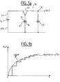
La figure 1a illustre une représentation d'un schéma de circuit de base d'un circuit de pompe de charge 10. Ce circuit de pompe de charge 10 comprend une alimentation en tension 5, procurant une tension Vin, un commutateur unipolaire à deux contacts S1 et des premier et second condensateurs C1, C2.Figure 1a illustrates a representation of a basic circuit diagram of a charge pump circuit 10. This charge pump circuit 10 comprises a
De façon à mettre en évidence ce problème de non linéarité, considérons un instant t(n) où le commutateur S1 occupe sa première position indiquée par une ligne en traits pleins, reliant le condensateur C1 à l'alimentation en tension 5. De ce fait, la première plaque 12 du condensateur C1 est reliée à la borne de tension positive Vin de l'alimentation en tension 5. La seconde plaque 14 du condensateur C1 est reliée en permanence à la borne de tension négative VSS de l'alimentation en tension 5. Le second condensateur C2, lequel est isolé du condensateur C1, présente ses première et seconde plaques reliées entre une borne de sortie 16 du circuit de pompe de charge 10 et la borne de tension négative VSS. La borne de sortie 16 fournit la tension de sortie Vout. Ainsi, à l'instant t(n), le condensateur C1 se charge jusqu'à la valeur de tension Vin, en supposant que VSS soit référencée à la masse, c'est-à-dire 0 V. Pendant cet intervalle de temps, le condensateur C2 supporte la tension Vout(n) et la charge totale stockée par les condensateurs C1 et C2 est donnée par Qt(n)=[C1.Vin + C2.Vout(n)].In order to highlight this problem of non-linearity, let us consider an instant t (n) where the switch S1 occupies its first position indicated by a line in solid lines, connecting the capacitor C1 to the
Par suite, à l'instant t(n+1), le commutateur S1 passe de sa première position à sa seconde position, la seconde position étant indiquée par des lignes en pointillés. Les condensateurs C1 et C2 sont à présent reliés en parallèle entre la borne de sortie 16 et la borne de tension négative VSS et les deux condensateurs (C1, C2) sont isolés de l'alimentation en tension 5. Ainsi, la charge totale qui a été stockée par les condensateurs C1 et C2 à l'instant t(n), c'est-à-dire Qt(n), est à présent partagée entre les condensateurs C1 et C2 et il en résulte que la tension Vout s'accroit depuis une valeur Vout(n) vers une valeur Vout(n+1). A partir du principe de la conservation de la charge, on obtient l'équation suivante :![]()
![]()
![]()
![]()
A partir de l'équation 1, on peut voir que le terme de gauche [Vout(n+1)-Vout(n)] décroît avec le temps du fait que le terme de droite Vout(n) s'approche de Vin.From
La figure 1b illustre une représentation graphique de la vitesse de variation de la tension de programmation Vout en fonction du temps, c'est-à-dire dVout/dt. Il faut noter que la hauteur de variation initiale du saut de la tension Vout est beaucoup plus grande que la hauteur de variation du saut de la tension Vout vers la fin de son accroissement. La ligne en pointillés indique l'enveloppe de la vitesse de variation dVout/dt de la tension Vout, laquelle est donnée par Vout = Vin(1-exp(-t/x)), dans lequel x est proportionnel à [C1+C2]/C1.FIG. 1b illustrates a graphic representation of the speed of variation of the programming voltage Vout as a function of time, that is to say dVout / dt. It should be noted that the initial height of variation of the jump in voltage Vout is much greater than the height of variation of the jump in voltage Vout towards the end of its increase. The dotted line indicates the envelope of the speed of variation dVout / dt of the voltage Vout, which is given by Vout = Vin (1-exp (-t / x)), in which x is proportional to [C1 + C2 ] / C1.
Il est ainsi montré qu'un circuit de pompe de charge ne produit pas une rampe linéaire. Même si la tension d'alimentation est élevée, il n'en reste pas moins que sa rampe n'est pas linéaire et ne peut pas être utilisée telle quelle pour programmer des cellules mémoire de l'EPROM.It is thus shown that a charge pump circuit does not produce a linear ramp. Even if the supply voltage is high, the fact remains that its ramp is not linear and cannot be used as it is for programming EPROM memory cells.
En fait, la tension VPP est produite, à partir d'une tension HI-V existante (à l'extérieur ou à l'intérieur du circuit intégré), par un circuit comportant un condensateur alimenté par une source de courant constant laquelle est alimentée par cette tension HI-V. Un tel circuit souffre des inconvénients d'être analogique et de la nécessité du contrôle du temps lorsque VPP atteint sa valeur nominale, et du contrôle de la durée d'une valeur en palier. Ceci est également obtenu par des circuits analogiques qui sont difficiles à régler à cause de la dispersion des caractéristiques.In fact, the VPP voltage is produced, from an existing HI-V voltage (outside or inside the integrated circuit), by a circuit comprising a capacitor supplied by a constant current source which is supplied by this voltage HI-V. Such a circuit suffers from the drawbacks of being analog and from the need to control the time when VPP reaches its nominal value, and to control the duration of a level value. This is also achieved by analog circuits which are difficult to adjust due to the dispersion of the characteristics.
Par conséquent, un but de la présente invention est d'engendrer une tension de rampe qui est obtenue à partir d'une tension donnée. La tension donnée peut, mais ceci n'est pas nécessaire, présenter une valeur inférieure à la tension de rampe nominale. Le moyen pour engendrer la tension de rampe comprend un moyen pour échantillonner la tension donnée et un moyen pour réguler la tension de rampe à une valeur souhaitée. Le moyen pour échantillonner la tension donnée est relié, commandé et encore dirigé de façon telle que la tension de rampe s'accroisse d'une façon commandée graduellement, l'accroissement graduel de la tension de rampe étant pratiquement linéaire.Therefore, an object of the present invention is to generate a ramp voltage which is obtained from a given voltage. The given voltage can, but this is not necessary, have a value lower than the nominal ramp voltage. The means for generating the ramp voltage includes means for sampling the given voltage and means for regulating the ramp voltage to a desired value. The means for sampling the given voltage is connected, controlled and further directed so that the ramp voltage increases in a gradually controlled manner, the gradual increase in the ramp voltage being substantially linear.
L'invention a donc pour objet un générateur de rampe numérique caractérisé en ce qu'il comprend un circuit d'échantillonnage commandé qui reçoit une tension d'entrée et produit une tension échantillonnée, un circuit d'addition pour additionner ladite tension échantillonnée à une tension de sortie du générateur (VPP) afin de procurer une tension nouvelle qui est supérieure à ladite tension d'entrée, et un circuit de transmission, ou circuit suiveur de tension, recevant ladite tension nouvelle et ladite tension de sortie du générateur et procurant une autre tension de sortie du générateur supérieure à la précédente tension de sortie du générateur.The subject of the invention is therefore a digital ramp generator characterized in that it comprises a controlled sampling circuit which receives an input voltage and produces a sampled voltage, an addition circuit for adding said sampled voltage to a generator output voltage (VPP) to provide a new voltage which is greater than said input voltage, and a transmission circuit, or voltage follower circuit, receiving said new voltage and said generator output voltage and providing a another generator output voltage greater than the previous generator output voltage.
La présente invention propose un générateur de rampe numérique qui comprend un circuit d'échantillonnage, lequel reçoit une première tension d'entrée qui doit être échantillonnée de façon à obtenir une tension échantillonnée correspondant à une charge électrique et un circuit de transmission, lequel reçoit et transmet la charge électrique depuis le circuit d'échantillonnage vers une sortie du générateur afin de produire une tension de sortie en rampe. Un circuit élévateur reçoit la tension de sortie en rampe et l'ajoute à la tension échantillonnée. Un circuit de commande commande les fonctionnalités des circuits d'échantillonnage, de transmission et élévateurs suivant des phases dans lesquelles,
- a) l'échantillonnage de la tension d'entrée se produit une première fois,
- b) une tension correspondant à la charge d'entrée échantillonnée est alors ajoutée à la tension d'entrée du circuit élévateur,
- c) la tension d'addition résultante est alors transmise par le circuit de transmission vers la sortie du générateur.
- a) the sampling of the input voltage occurs for the first time,
- b) a voltage corresponding to the sampled input load is then added to the input voltage of the booster circuit,
- c) the resulting addition voltage is then transmitted by the transmission circuit to the output of the generator.
Le but de la présente invention de même que d'autres buts, avantages et particularités seront mis en évidence à la lumière de la description détaillée suivante et des illustrations annexées, dont le but n'est pas limitatif, et dans lesquelles :The object of the present invention as well as other objects, advantages and features will be highlighted in the light of the following detailed description and of the appended illustrations, the aim of which is not limiting, and in which:
La figure 1a illustre une représentation déjà décrite d'un schéma d'un circuit de base d'un circuit de pompe de charge.FIG. 1a illustrates an already described representation of a diagram of a basic circuit of a charge pump circuit.
La figure 1b illustre une représentation graphique de la vitesse de variation de la tension de sortie Vout de la figure 1a.FIG. 1b illustrates a graphical representation of the rate of variation of the output voltage Vout of FIG. 1a.
La figure 2a illustre un générateur de rampe numérique conforme à la présente invention.Figure 2a illustrates a ramp generator digital according to the present invention.
La figure 2b illustre la vitesse de variation de la tension de programmation de la figure 2a en fonction du temps.FIG. 2b illustrates the speed of variation of the programming voltage of FIG. 2a as a function of time.
La figuré 2c illustre la relation de cadencement des signaux de commande des trois commutateurs tels que décrits en relation avec les figures 2a et 2b.FIG. 2c illustrates the timing relationship of the control signals of the three switches as described in relation to FIGS. 2a and 2b.
Les figures 3a, 3b et 3c illustrent un exemple d'un schéma de circuit du générateur de rampe numérique de la figure 2a.Figures 3a, 3b and 3c illustrate an example of a circuit diagram of the digital ramp generator of Figure 2a.
La figure 4 représente les signaux utilisés pour commander les circuits des figures 3a à 3c.Figure 4 shows the signals used to control the circuits of Figures 3a to 3c.
La figure 5 représente un schéma synoptique d'un générateur de signal de commande qui est utilisé afin de produire les niveaux de tension de la figure 4.Figure 5 shows a block diagram of a control signal generator which is used to produce the voltage levels of Figure 4.
La figure 2a est une illustration représentative d'un générateur de rampe numérique conforme à la présente invention. Ce générateur de rampe numérique 20 comprend deux commutateurs unipolaires à deux contacts S20 et S22, un commutateur unipolaire à un contact S24, trois condensateurs C20, C22, C24 et un suiveur de tension 22.Figure 2a is a representative illustration of a digital ramp generator according to the present invention. This
Un premier contact du commutateur S20 repéré par le noeud 23 est relié à Vcc, son second contact est repéré par le noeud 24 et son noeud commun est repéré par le noeud 25. Dans une première position du commutateur S20, le noeud 25 est relié au noeud 23. Dans une seconde position, le noeud 25 est relié au noeud 24. Un premier contact du commutateur S22 est repéré par le noeud 26, son second contact est repéré par le noeud 27 et son noeud commun est repéré par le noeud 28. Dans une première position du commutateur S22, le noeud 28 est relié au noeud 26. Dans une seconde position, le noeud 28 est relié au noeud 27. Si le noeud 23 est relié à une entrée d'alimentation Vcc, le noeud 26 est relié à une entrée de masse, soit VSS. Le condensateur C22 est relié entre le noeud 24 et la tension de référence VSS. Le noeud 24 fournit une tension en rampe. Le suiveur de tension 22 reçoit cette tension en rampe sur une première entrée et procure une tension de sortie en rampe VPP sur sa borne de sortie 29. La borne de sortie 29 est reliée à une seconde entrée du suiveur de tension 22. Le suiveur de tension 22 pourrait être un amplificateur opérationnel relié en suiveur de tension. Schématiquement, le suiveur de tension 22 est alimenté par une tension d'entrée élevée HI-V. Le commutateur 24 est relié en série entre les noeuds 27 et 29 et le condensateur C24 est relié entre le noeud 27 et la référence de tension VSS. Le condensateur C20 est relié entre les noeuds 25 et 28 des commutateurs S20 et S22, respectivement. En pratique, une tension d'alimentation en programmation non régulée HI est régulée à sa valeur requise HI-V par des moyens non représentés.A first contact of the switch S20 identified by the
Le fonctionnement de base du générateur de rampe 20 conforme à l'invention peut être décomposé en une série d'intervalles de temps. La description suivante ne prend en compte ni le seuil relativement petit et pratiquement constant, ni les pertes de commutation, etc.. A l'instant t0, (Figure 2b), on peut supposer que tous les condensateurs, C20, C22, C24 sont complètement déchargés, isolés physiquement les uns des autres, et que la valeur de la capacité du condensateur C24 est supérieure à celle de C22, dont la capacité est elle-même de valeur supérieure à celle de C20. En outre, les commutateurs S20, S22 et S24 sont supposés être commandés par les signaux de commande respectifs Φ1, Φ2 et Φ3 apparaissant sur la figure 2c.The basic operation of the
La figure 2b illustre la vitesse de variation de la tension de programmation de la figure 2a en fonction du temps.FIG. 2b illustrates the speed of variation of the programming voltage of FIG. 2a as a function of time.
Dans l'intervalle de temps défini par t0 < t < t1, les commutateurs S20 et S22 sont dans leur première position respective, comme indiqué par une ligne continue, et le commutateur S24 est ouvert : ainsi, les trois condensateurs C20, C22, C24 sont tous physiquement isolés les uns des autres. La plaque positive 25 du condensateur C20 se charge jusqu'à la valeur de tension Vcc, en supposant que la tension VSS est référencée par rapport à la masse par l'intermédiaire du commutateur S22.In the time interval defined by t0 <t <t1, switches S20 and S22 are in their respective first position, as indicated by a solid line, and switch S24 is open: thus, the three capacitors C20, C22, C24 are all physically isolated from each other. The
A l'instant t1, les commutateurs S20 et S22 basculent, au même instant, ou pratiquement au même instant, depuis leur première position respective vers leur seconde position respective, comme indiqué par des lignes en pointillés; le commutateur S24 reste ouvert.At time t1, the switches S20 and S22 switch, at the same time, or practically at the same time, from their first respective position to their second respective position, as indicated by dotted lines; switch S24 remains open.
Dans l'intervalle de temps défini par t1 < t < t2 pendant lequel les commutateurs S20 et S22 sont dans leur seconde position respective et le commutateur S24 est ouvert, les condensateurs C24 et C20 sont maintenant reliés en série. En outre, cet ensemble de condensateurs C24 et C20 reliés en série est relié en parallèle avec le condensateur C22. La plaque positive 27 du condensateur C24 est reliée à la plaque négative 28 du condensateur C20. De ceci il résulte que la plaque positive 25 du condensateur C20 est amenée à un niveau de tension qui est supérieur au niveau de tension VPP disponible précédemment à la sortie du comparateur 22.In the time interval defined by t1 <t <t2 during which the switches S20 and S22 are in their respective second position and the switch S24 is open, the capacitors C24 and C20 are now connected in series. In addition, this set of capacitors C24 and C20 connected in series is connected in parallel with the capacitor C22. The
Cependant, au début, pendant ce premier intervalle de temps particulier, la tension aux bornes du condensateur C24 est de zéro Volt. De ce fait, aucune élevation de tension ne se produit. Néanmoins, à partir du principe de la conservation de charge, on peut obtenir l'équation suivante :![]()
![]()
Cette équation 2 reste vraie même pendant les cycles suivants. On notera que l'équation 2 ne contient pas de terme VPP(t) à droite, à la différence de l'équation 1. L'absence de terme VPP(t) dans le membre de droite de l'équation 2 est à l'origine de la grande amélioration de la linéarité de la pente de la tension VPP, c'est-à-dire dVPP/dt.This
De ce fait, en intégrant l'équation 2 on obtient![]()
![]()
Comme l'implique le terme suiveur de tension, la tension VPP sur la borne de sortie 29 du suiveur de tension 22 suit ou poursuit la tension sur sa borne d'entrée 24. De ce fait, comme la borne d'entrée du suiveur de tension 22 est reliée au noeud 24, la tension VPP sur la borne de sortie 29 du suiveur de tension 22 est pratiquement égale à la tension donnée par l'équation 3.As the term voltage follower implies, the voltage VPP on the
A l'instant t2, les commutateurs S20 et S22 basculent de leur seconde position respective et retournent vers leur première position respective, le commutateur S24 reste ouvert. Ainsi, les trois condensateurs, C20, C22, C24, sont à nouveau tous isolés les uns des autres. En outre, le condensateur C20 commence à nouveau à se charger vers la valeur de tension Vcc, il recommence à prendre un échantillon de la tension Vcc.At time t2, the switches S20 and S22 switch from their respective second position and return to their respective first position, the switch S24 remains open. Thus, the three capacitors, C20, C22, C24, are again all isolated from each other. In addition, the capacitor C20 again begins to charge towards the voltage value Vcc, it begins again to take a sample of the voltage Vcc.
Dans l'intervalle défini par t2 < t < t3 : les commutateurs S20 et S22 sont dans leur première position respective, la plaque positive 25 du condensateur C20 se recharge à la valeur de tension Vcc. Le palier t2-t3 peut être très court par comparaison avec le palier t0-t1, t1-t2, ou le palier suivant t3-t4.In the interval defined by t2 <t <t3: the switches S20 and S22 are in their first respective position, the
A l'instant t3, les commutateurs S20 et S22 restent toujours dans leur première position respective, le commutateur S24 se ferme et relie la borne de sortie 29 du suiveur de tension 22 à la plaque la plus positive 27 du condensateur C24.At time t3, the switches S20 and S22 always remain in their first respective position, the switch S24 closes and connects the
Dans l'intervalle de temps défini par t3<t<t4, le condensateur C24 est chargé par la tension VPP du suiveur de tension présente sur la borne de sortie 29 du suiveur de tension 22. C'est-à-dire qu'il se charge pratiquement à la valeur de tension donnée par l'équation 3. Les charges électriques proviennent de l'alimentation HI-V.In the time interval defined by t3 <t <t4, the capacitor C24 is charged by the voltage VPP of the voltage follower present on the
A l'instant t4, les commutateurs S20 et S22 étant toujours dans leur première position respective, le commutateur S24 s'ouvre et déconnecte la borne de sortie 29 du suiveur de tension 22 de la plaque la plus positive 27 du condensateur C24, lequel conserve pratiquement sa charge.At time t4, the switches S20 and S22 being always in their first respective position, the switch S24 opens and disconnects the
Dans l'intervalle de temps défini par t4 < t < t5, les commutateurs S20 et S22 restent dans leur première position respective et le commutateur S24 reste ouvert. Il se produit un même phénomène que pendant l'intervalle de temps t0-t1, excepté que le noeud 27 n'est plus à VSS mais est amené à la valeur VPP.In the time interval defined by t4 <t <t5, the switches S20 and S22 remain in their first respective position and the switch S24 remains open. The same phenomenon occurs as during the time interval t0-t1, except that the
A l'instant t5, les commutateurs S20 et S22 basculent de leur première position respective vers leur seconde position respective comme décrit ci-dessus pour l'instant t1.At time t5, the switches S20 and S22 switch from their first respective position to their second respective position as described above. for the moment t1.
Dans l'intervalle de temps défini par t5 < t < t6, les commutateurs S20 et S22 étant dans leur seconde position respective et le commutateur S24 étant ouvert, les condensateurs C20 et C24 en série sont à présent reliés à nouveau en série. Cet ensemble de condensateurs C20 et C24 est relié en parallèle avec le condensateur C22 comme décrit ci-dessus pour l'intervalle de temps t1 < t < t2. Cependant, pendant cet intervalle de temps le condensateur C24 se charge à la tension donnée par l'équation 3, soit VPP de telle sorte que le condensateur C24 élève la plaque négative du condensateur C20 jusqu'à cette valeur de tension. L'effet de pompage ou d'élevation est que la plaque négative 28 du condensateur C20 est toujours référencée par rapport à la tension VPP de programmation précédente lorsque les commutateurs S20 et S22 sont dans leur seconde position respective. Exprimé en termes plus généraux, le condensateur d'échantillonnage d'entrée C20 comporte toujours une plaque négative 28 référencée soit à la masse, soit, au moyen d'un condensateur d'élevation de sortie C24, à la valeur courante de la tension de sortie VPP de telle façon que la tension d'entrée Vcc soit ajoutée à la tension de sortie courante VPP.In the time interval defined by t5 <t <t6, the switches S20 and S22 being in their respective second position and the switch S24 being open, the capacitors C20 and C24 in series are now connected again in series. This set of capacitors C20 and C24 is connected in parallel with the capacitor C22 as described above for the time interval t1 <t <t2. However, during this time interval the capacitor C24 charges at the voltage given by
A l'instant t6, les commutateurs S20 et S22 basculent de leur seconde position respective et retournent vers leur première position respective et le commutateur S24 reste ouvert comme décrit ci-dessus pour l'instant t2.At time t6, switches S20 and S22 switch from their respective second position and return to their first respective position and switch S24 remains open as described above for time t2.
Dans l'intervalle de temps défini par t6 < t < t7 : les commutateurs S20 et S22 sont dans leur première position respective, le commutateur S24 est ouvert et les trois condensateurs C20, C22 et C24 se trouvent tous isolés physiquement les uns des autres. La plaque positive 25 du condensateur C20 se recharge à la valeur de tension Vcc.In the time interval defined by t6 <t <t7: the switches S20 and S22 are in their first respective position, the switch S24 is open and the three capacitors C20, C22 and C24 are all physically isolated from each other. The plaque positive 25 of capacitor C20 recharges at the voltage value Vcc.
A l'instant t7, le commutateur S24 se ferme et relie la borne de sortie 29 du suiveur de tension 22 à la plaque positive 27 du condensateur C24 comme décrit ci-dessus pour l'instant t3, et ainsi de suite.At time t7, the switch S24 closes and connects the
La figure 2c illustre la relation de cadencement des signaux de commande respectifs Φ1, Φ2 et Φ3 des commutateurs respectifs S20, S22 et S24 comme décrits en relation avec les figures 2a et 2b. La durée d'un cycle va de l'instant tl à l'instant t5.Figure 2c illustrates the timing relationship of the respective control signals Φ1, Φ2 and Φ3 of the respective switches S20, S22 and S24 as described in connection with Figures 2a and 2b. The duration of a cycle goes from time tl to time t5.
On notera, à partir de la figure 2c, qu'il n'est pas obligatoire d'inclure le commutateur S24. Il pourrait en théorie être remplacé par un court-circuit si les commutateurs S20 et S22 étaient commandés de telle façon que le commutateur S20 ne soit jamais dans sa première position lorsque le commutateur S22 est dans sa seconde position (et vice versa). Bien que cela conduise à un circuit instable dans certains cas, cela pourrait fonctionner.It will be noted from FIG. 2c that it is not compulsory to include the switch S24. It could in theory be replaced by a short circuit if the switches S20 and S22 were controlled so that the switch S20 is never in its first position when the switch S22 is in its second position (and vice versa). Although this leads to an unstable circuit in some cases, it could work.
La figure 3a illustre un exemple d'un schéma de circuit du générateur de rampe numérique de la figure 2a. Ce schéma de circuit représente six transistors CMOS du type N MN1 à MN6, une diode D et les trois condensateurs C20, C22 et C24.Figure 3a illustrates an example of a circuit diagram of the digital ramp generator of Figure 2a. This circuit diagram shows six N-type CMOS transistors MN1 to MN6, a diode D and the three capacitors C20, C22 and C24.
En se référant au transistor MN1, sa borne de source représente le noeud 23 et est reliée de préférence à une tension d'alimentation VZ. La tension VZ est produite par le circuit de la figure 3b. La valeur de VZ est de l'ordre de Vcc mais sous forme pulsée. La borne de drain de MN1 représente le noeud 25 et est reliée à la plaque positive du condensateur C20. En se référant au transistor MN2, sa borne de drain représente le noeud 25 et sa borne de source représente le noeud 24, lequel est relié à la plaque positive du condensateur C22. Les transistors MN1 et MN2 sont reliés et commandés de telle manière qu'ils représentent le commutateur S20 de la figure 2a. Les bornes de grille respectives des transistors MN1 et MN2 sont commandées par les signaux de commande respectifs Φ1 et NΦ1. Le signal NΦ1 est le signal inverse de Φ1. Ceux-ci sont engendrés par le circuit de la figure 3c.Referring to transistor MN1, its source terminal represents
En se référant au transistor MN3, sa borne de drain représente le noeud 28 et est reliée à la plaque négative du condensateur C20, sa borne de source représente le noeud 26 et est reliée à la borne de tension négative VSS. En se référant au transistor MN4, sa borne de source représente le noeud 28 et sa borne de drain représente le noeud 27, lequel est relié à la plaque positive du condensateur C24. Les transistors MN3 et MN4 sont reliés et commandés de telle façon qu'ils représentent le commutateur S22 de la figure 2a. Les bornes de grille respectives des transistors MN3 et MN4 sont commandées par les signaux de commande respectifs Φ2 et NΦ2. Le signal NΦ2 est le signal inverse de Φ2. Ceux-ci peuvent également être produits par le circuit de la figure 3c.Referring to the transistor MN3, its drain terminal represents the
Le transistor MN5 est relié et commandé de telle façon qu'il représente le suiveur de tension 22 de la figure 2a. En se référant au transistor MN5, sa borne de drain est reliée, par l'intermédiaire de la diode D, au noeud 25, c'est-à-dire la plaque positive du condensateur C20. Sa borne de grille est reliée au noeud 24, c'est-à-dire la plaque positive du condensateur C22, et sa borne de source représente le noeud 29. Sa borne de drain est reliée à un noeud HI-V. La diode D est représentée par un transistor CMOS du type N branché en diode dans le sens direct dont l'anode, qui est reliée au noeud 25, est formée en reliant les bornes de grille et de drain ensemble, la cathode de cette diode, c'est-à-dire la borne de source, est reliée à la borne de drain du transistor MN5 et au noeud HI-V. Il est préférable d'inclure cette diode D dans la mesure où elle empêche toute surtension de se produire au noeud 25, laquelle peut être produite par l'effet d'élevation.The transistor MN5 is connected and controlled in such a way that it represents the
Le transistor MN6 est relié et commandé de telle façon qu'il représente le commutateur S24 de la figure 2a. En se référant au transistor MN6, sa borne de drain est reliée à la borne de source 29 du transistor MN5, sa borne de source est reliée à la plaque positive 24 du condensateur C24 et sa borne de grille est commandée par le signal de commande Φ3.The transistor MN6 is connected and controlled so that it represents the switch S24 in FIG. 2a. Referring to transistor MN6, its drain terminal is connected to the
Les signaux de commande Φ1, NΦ1, Φ2, NΦ2 et Φ3 sont de préférence obtenus à partir de circuits qui sont alimentés à partir de la tension élevée HI-V, comme décrit ci-après.The control signals Φ1, NΦ1, Φ2, NΦ2 and Φ3 are preferably obtained from circuits which are supplied from the high voltage HI-V, as described below.
Il faut noter que les transistors MN1 à MN6 sont des transistors CMOS symétriques et que leurs bornes de drain et de source respectives peuvent être respectivement interchangées. En outre, il est préférable que les transistors MN2 et MN5 soient des transistors MOS du type N natif c'est-à-dire, des transistors qui n'ont pas fait l'objet d'ajustement de tension de seuil de grille (Vth) et, en conséquence, ont un seuil de conduction faible.It should be noted that the transistors MN1 to MN6 are symmetrical CMOS transistors and that their respective drain and source terminals can be respectively interchanged. Furthermore, it is preferable that the transistors MN2 and MN5 are native N-type MOS transistors, that is to say transistors which have not been subject to gate threshold voltage adjustment (Vth ) and, consequently, have a low conduction threshold.
La figure 3b représente un circuit utilisé de préférence pour produire une tension à une valeur VZ. Du fait que des charges électriques identiques constituent le principe de base d'un signal de rampe linéaire, le condensateur d'échantillonnage C20 doit être alimenté de préférence par une tension constante.FIG. 3b represents a circuit preferably used to produce a voltage at a value VZ. Since identical electrical charges constitute the basic principle of a linear ramp signal, the sampling capacitor C20 should preferably be supplied with a constant voltage.
Comme représenté, l'alimentation VZ est produite par une diode Zener DZ, reliée entre un noeud de tension HI-V et un noeud de tension VSS, en série avec un transistor CMOS du type P MP6. En outre, un tel circuit consommant du courant, il est préférable qu'il soit commuté par un signal cyclique VE. Le signal VE permet la conduction du circuit MP6-DZ uniquement lorsque C20 doit être chargé : lorsque les commutateurs S20 et S22 basculent vers leur première position.As shown, the VZ power supply is produced by a Zener DZ diode, connected between a node HI-V voltage and a VSS voltage node, in series with a P type MP6 CMOS transistor. Furthermore, since such a circuit consumes current, it is preferable for it to be switched by a cyclic signal VE. The signal VE allows the conduction of the MP6-DZ circuit only when C20 must be charged: when the switches S20 and S22 switch to their first position.
De façon caractéristique, cette conduction se produit pendant trois microsecondes toutes les 16 microsecondes. La conduction est obtenue au moyen d'un miroir de courant comprenant le transistor MP6 dans la branche de la diode DZ et un transistor MP5 dans une branche comprenant en outre une série de deux transistors MOS du type N MN12 et MN13. Le transistor MN12 est utilisé pour conditionner la conduction de la diode DZ à la réception de signaux VE sur sa grille. La grille du transistor MP5 est connectée à la grille du transistor MP6 et à son propre drain. Le transistor MP5 agit comme un générateur de courant dont la valeur est fixée par une tension constante Vref apparaissant sur la grille du transistor MN13. La tension constante Vref est elle-même produite par un circuit miroir de WILSON classique comprenant des transistors CMOS du type P MP1 à MP4 et des transistors CMOS du type N MN10, MN11 et MN14. Ce miroir de WILSON est lui-même commuté par un signal VF qui est appliqué à la grille du transistor de copie MP1 et MP2. Lorsqu'une tension VPP n'est pas nécessaire, VF est à VZ et les transistors MP1 et MP2 sont bloqués. Lorsque VPP est nécessaire, VF est fixé à VSS. Le fait d'avoir une tension Vref stable, laquelle attaque un circuit qui lui-même procure une tension stable VZ, permet d'obtenir un courant de conduction faible dans la diode DZ sans subir les inconvénients d'une modification de la tension DZ dûs à une modification de ce courant faible.Typically, this conduction occurs for three microseconds every 16 microseconds. Conduction is obtained by means of a current mirror comprising the transistor MP6 in the branch of the diode DZ and a transistor MP5 in a branch further comprising a series of two MOS transistors of the N type MN12 and MN13. The transistor MN12 is used to condition the conduction of the diode DZ on the reception of signals VE on its gate. The gate of the transistor MP5 is connected to the gate of the transistor MP6 and to its own drain. The transistor MP5 acts as a current generator whose value is fixed by a constant voltage Vref appearing on the gate of the transistor MN13. The constant voltage Vref is itself produced by a conventional WILSON mirror circuit comprising CMOS transistors of the P type MP1 to MP4 and CMOS transistors of the N type MN10, MN11 and MN14. This WILSON mirror is itself switched by a signal VF which is applied to the gate of the copy transistor MP1 and MP2. When a voltage VPP is not necessary, VF is at VZ and the transistors MP1 and MP2 are blocked. When VPP is required, VF is set to VSS. The fact of having a stable voltage Vref, which drives a circuit which itself provides a stable voltage VZ, makes it possible to obtain a low conduction current in the diode DZ without undergoing the drawbacks of a modification of the voltage DZ due to a modification of this weak current.
La figure 3c représente un circuit inverseur haute tension destiné à engendrer les signaux de commande à tension élevée Φx et NΦx. Dans le circuit de l'invention, deux circuits de ce type sont nécessaires pour attaquer les commutateurs S20 et S24 respectivement.FIG. 3c represents a high voltage inverter circuit intended to generate the high voltage control signals Φx and NΦx. In the circuit of the invention, two circuits of this type are necessary to drive the switches S20 and S24 respectively.
L'inverseur haute tension 400 représenté comprend : un étage croisé 410; un étage cascode 420; et un étage de commutation 430. Il procure les signaux de tension élevée complémentaires Φx, NΦx.The
L'étage croisé 410 est relié à la tension HI-V et procure deux signaux de sortie complémentaires à tension élevée OUT et NOUT sur ses bornes de sortie respectives 440 et 450. L'étage croisé 410 comporte deux transistors MOS du type P croisés MP40 et MP41 dont les sources sont reliées à la tension HI-V. La grille du transistor MP40 est reliée au drain 440 du transistor MP41 et la grille du transistor MP41 est reliée au drain 450 du transistor MP40.The cross stage 410 is connected to the HI-V voltage and provides two complementary high-voltage output signals OUT and NOUT on its
Deux entrées respectives de l'étage cascode 420 sont reliées aux sorties respectives 440 et 450 de l'étage croisé 410. L'étage cascode 420 fournit les signaux de commande complémentaires à tension élevée Φx et NΦx sur ses bornes respectives 460 et 470. L'étage cascode 420 comprend deux transistors MOS du type P MP42 et MP43 dont les bornes de source sont respectivement reliées aux bornes de drain des transistors MP40 et MP41 et dont les bornes de grille sont polarisées par l'intermédiaire de la borne 480 par une tension de référence Vrefl.Two respective inputs of the
Vref1 est égale à HI-V moins environ 5 volts. Les drains des transistors MOS MP40 et MP41 de l'étage 410 sont ainsi polarisés de façon à ne pas être à une tension trop basse. Ceci limite le courant de commutation et accroit de ce fait l'efficacité puisque le circuit est alimenté par la source de tension HI-V dont la sortance est faible.Vref1 is equal to HI-V minus around 5 volts. The drains of the MOS transistors MP40 and MP41 of stage 410 are thus polarized so as not to be at one voltage too low. This limits the switching current and thereby increases the efficiency since the circuit is supplied by the HI-V voltage source whose fan-out is low.
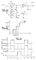
Deux bornes d'entrée respectives de l'étage de commutation 430 sont reliées aux bornes de sortie respectives 460 et 470 de l'étage cascode 420. L'étage de commutation 430 est commandé par l'intermédiaire d'une troisième borne d'entrée 490, par un signal de commande d'entrée VC ou VD (selon les signaux Φ1 ou Φ2 à produire) et est relié à la source de tension VSS. Les niveaux de tension des signaux de commande d'entrée VC ou VD sont de préférence obtenus à partir de la source de tension Vcc.Two respective input terminals of the switching
L'étage de commutation 430 comprend deux transistors MOS du type N MN40 et MN41 et un inverseur INV1, de préférence un inverseur CMOS. Les bornes de drain des transistors MN40 et MN41 sont respectivement reliées aux bornes de source des transistors MP42 et MP43. Les signaux de commande VC ou VD sont appliqués à la borne de grille du transistor MN40 et à la borne d'entrée de l'inverseur INV1. La borne de grille du transistor MN41 est reliée à la borne de sortie 495 de l'inverseur INV1. Un pôle d'alimentation haute de l'inverseur INV1 est relié à la source de tension VCC, alors que le pôle d'alimentation basse de l'inverseur INV1 est relié à la source de tension VSS.The switching
Du fait que le fonctionnement du circuit inverseur de haute tension 400 est symétrique, seul son fonctionnement dans un état logique stable haut, c'est-à-dire un niveau de tension de VCC, présent sur la borne de grille 490 du transistor MN40 sera envisagé, puisqu'une personne expérimentée dans la technique peut facilement déduire le cas inverse.Since the operation of the high-
De ce fait, le transistor MN40 est conducteur alors que le transistor MN41 n'est pas conducteur. Ainsi, le transistor MN40 abaisse la tension sur la borne de drain 470 du transistor MP42 jusqu'à un niveau approximativement égal à VSS. Du fait que le transistor MP42 (et en fait le transistor MP43) est commuté par Vrefl par l'intermédiaire de la borne 480, il est conducteur, il en résulte que la tension du noeud 450 est abaissée jusqu'à un niveau approximativement égal à VPP-Vref1+Vtp. Le supplément Vtp est dû au fait que les caissons dans lesquels sont fabriqués les transistors P MP40 etMP43 sont portés à HI-V. Du fait que les bornes respectives de drain et de grille des transistors respectifs MP40 et MP41 sont croisées, l'action d'abaisser la tension de l'une des grilles de l'un de ces transistors entraîné la tension de l'autre à s'élever, ainsi des signaux complémentaires OUT et NOUT sont procurés. Dans ce mode de réalisation particulier, le signal de commande Φx est à un niveau de tension approximativement égal à VPP, alors que le signal de commande NΦx est à un niveau de tension approximativement égal à VSS. Les signaux Φx et NΦx sont en opposition de phase alors que les signaux Φx et VC ou VD sont en phase.Therefore, the transistor MN40 is conductive while the transistor MN41 is not conductive. Thus, the transistor MN40 lowers the voltage on the
A partir de la figure 3a, on peut voir que le signal de commande NΦ2 peut être le signal de commande Φ1 et le signal de commande NΦ1 peut être le signal de commande Φ2. Ainsi, ces quatre signaux de commande Φ1, NΦ1, Φ2, NΦ2 peuvent être obtenus à partir d'un même circuit convertisseur de niveau de tension; le signal de commande Φ3 étant obtenu à partir d'un autre inverseur de haute tension. En variante, les signaux de commande Φ1, NΦ1 et Φ2, NΦ2 peuvent être obtenus à partir d'inverseurs de haute tension différents. En outre, il est possible que le transistor MN6 de la figure 3 soit commandé par le signal de commande Φ2 (ou NΦ1) à la place de Φ3.From FIG. 3a, it can be seen that the control signal NΦ2 can be the control signal Φ1 and the control signal NΦ1 can be the control signal Φ2. Thus, these four control signals Φ1, NΦ1, Φ2, NΦ2 can be obtained from the same voltage level converter circuit; the control signal Φ3 being obtained from another high voltage inverter. As a variant, the control signals Φ1, NΦ1 and Φ2, NΦ2 can be obtained from different high voltage inverters. In addition, it is possible that the transistor MN6 in FIG. 3 is controlled by the control signal Φ2 (or NΦ1) instead of Φ3.
La figure 4 représente des chronogrammes des signaux VC, VD, VE et VF présentés ci-dessus. VF est bas lorsqu'une sortie VPP doit être produite sous forme d'une rampe. VE, lequel déclenche la conduction de DZ, est actif à la fin d'une impulsion active VD, qui elle-même déclenche les commutateurs S20 et S22. Ainsi, lorsque VD est actif, et dès que VE devient actif, le condensateur C20 se charge. Ensuite, lorsque VD est bas, VC s'élève jusqu'à une tension élevée. Une tension élevée correspondant à VC est appliquée à MN6 agissant en tant que commutateur S24. Sur un niveau VC actif, S24 est fermé.FIG. 4 represents chronograms of the signals VC, VD, VE and VF presented above. VF is low when a VPP output is to be produced as a ramp. VE, which triggers the conduction of DZ, is active at the end of an active pulse VD, which itself triggers the switches S20 and S22. Thus, when VD is active, and as soon as VE becomes active, the capacitor C20 charges. Then, when VD is low, VC rises to a high voltage. A high voltage corresponding to VC is applied to MN6 acting as switch S24. On an active VC level, S24 is closed.
La figure 5 représente un schéma synoptique d'un générateur de signal de commande 500 qui est utilisé pour engendrer les signaux de la figure 4. Le générateur 500 comprend un oscillateur 510, un compteur 520 et un décodeur 530.FIG. 5 represents a block diagram of a
L'oscillateur 510 attaque le compteur 520 et le décodeur 530 reçoit du compteur 520 une pluralité de signaux en entrée I1 à In et le décodeur 530 délivre une pluralité de signaux de commande VC à VF qui présentent les relations de cadencement appropriées. Le décodeur 530 et le compteur 520 sont connus des personnes expérimentées dans la technique.The
Le fonctionnement du générateur de rampe numérique peut être commandé par un signal MARCHE/ARRET qui est reçu par le compteur 520.The operation of the digital ramp generator can be controlled by an ON / OFF signal which is received by the
De ce fait, à condition que la sortie de l'oscillateur 510 soit stable, la vitesse de variation de la tension de programmation VPP, c'est-à-dire dVPP/dt, ne dépendra que du rapport des capacités C20 et C22, c'est-à-dire C20/C22, qui est un rapport de surfaces qui peut être maîtrisé avec précision. Comme résultat de cette dépendance du rapport des surfaces des condensateurs C20 et C22, le générateur de rampe numérique conforme à l'invention est indépendant de toutes variations de processus, de température et de tension d'alimentation (VCC) et la tension de programmation VPP à la sortie 24 du générateur de rampe numérique est pratiquement linéaire.Therefore, provided that the output of
Claims (12)
Applications Claiming Priority (2)
| Application Number | Priority Date | Filing Date | Title |
|---|---|---|---|
| FR9506498 | 1995-05-31 | ||
| FR9506498A FR2734941B1 (en) | 1995-05-31 | 1995-05-31 | DIGITAL RAMP GENERATOR. |
Publications (3)
| Publication Number | Publication Date |
|---|---|
| EP0745996A2 true EP0745996A2 (en) | 1996-12-04 |
| EP0745996A3 EP0745996A3 (en) | 1997-03-12 |
| EP0745996B1 EP0745996B1 (en) | 1999-04-07 |
Family
ID=9479569
Family Applications (1)
| Application Number | Title | Priority Date | Filing Date |
|---|---|---|---|
| EP96401155A Expired - Lifetime EP0745996B1 (en) | 1995-05-31 | 1996-05-29 | Digital ramp generator |
Country Status (4)
| Country | Link |
|---|---|
| US (1) | US5774390A (en) |
| EP (1) | EP0745996B1 (en) |
| DE (1) | DE69601976T2 (en) |
| FR (1) | FR2734941B1 (en) |
Cited By (2)
| Publication number | Priority date | Publication date | Assignee | Title |
|---|---|---|---|---|
| EP0862270A1 (en) * | 1997-02-28 | 1998-09-02 | STMicroelectronics S.r.l. | Staircase adaptive voltage generator circuit |
| EP1017172A1 (en) * | 1998-12-29 | 2000-07-05 | STMicroelectronics S.r.l. | Integrated circuit generating at least a voltage linear ramp having a slow rise |
Families Citing this family (5)
| Publication number | Priority date | Publication date | Assignee | Title |
|---|---|---|---|---|
| FR2738386B1 (en) * | 1995-09-05 | 1997-10-24 | Sgs Thomson Microelectronics | METHOD AND CIRCUIT FOR PROGRAMMING AND DELETING A MEMORY |
| EP1058271B1 (en) | 1999-06-04 | 2004-12-15 | STMicroelectronics S.r.l. | CMOS switch circuit for transferring high voltages, in particular for line decoding in nonvolatile memories, with reduced consumption during switching |
| FI107478B (en) * | 1999-12-03 | 2001-08-15 | Nokia Networks Oy | Digital ramp generator with power output control |
| DE10227375A1 (en) | 2002-06-20 | 2004-01-15 | Infineon Technologies Ag | Input voltage increasing method for integrated circuit uses charge pump for pre-charging capacitor and for converting its stored charge to be transferred to output capacitor |
| US7230561B2 (en) * | 2005-01-27 | 2007-06-12 | Micron Technology, Inc. | Programmable integrating ramp generator and method of operating the same |
Citations (1)
| Publication number | Priority date | Publication date | Assignee | Title |
|---|---|---|---|---|
| US5315547A (en) * | 1988-07-11 | 1994-05-24 | Hitachi, Ltd. | Nonvolatile semiconductor memory device with selective tow erasure |
-
1995
- 1995-05-31 FR FR9506498A patent/FR2734941B1/en not_active Expired - Fee Related
-
1996
- 1996-05-29 EP EP96401155A patent/EP0745996B1/en not_active Expired - Lifetime
- 1996-05-29 DE DE69601976T patent/DE69601976T2/en not_active Expired - Fee Related
- 1996-05-30 US US08/652,710 patent/US5774390A/en not_active Expired - Lifetime
Patent Citations (1)
| Publication number | Priority date | Publication date | Assignee | Title |
|---|---|---|---|---|
| US5315547A (en) * | 1988-07-11 | 1994-05-24 | Hitachi, Ltd. | Nonvolatile semiconductor memory device with selective tow erasure |
Non-Patent Citations (2)
| Title |
|---|
| EDN ELECTRICAL DESIGN NEWS, vol. 17, no. 19, 1 Octobre 1972, NEWTON, MASSACHUSETTS US, pages 48-49, XP002013828 EDWIN E MORRIS: "Simple stair generator uses 1 IC and 3 transistors" * |
| IEEE TRANSACTIONS ON CONSUMER ELECTRONICS, vol. 38, no. 4, Novembre 1992, NEW YORK US, pages 824-829, XP000324642 YOSHIOKA ET AL: "The development of a memory card for a digital still camera using a 4 Mbit NAND EEPROM" * |
Cited By (4)
| Publication number | Priority date | Publication date | Assignee | Title |
|---|---|---|---|---|
| EP0862270A1 (en) * | 1997-02-28 | 1998-09-02 | STMicroelectronics S.r.l. | Staircase adaptive voltage generator circuit |
| US5949666A (en) * | 1997-02-28 | 1999-09-07 | Sgs-Thomson Microelectronics S.R.L. | Staircase adaptive voltage generator circuit |
| EP1017172A1 (en) * | 1998-12-29 | 2000-07-05 | STMicroelectronics S.r.l. | Integrated circuit generating at least a voltage linear ramp having a slow rise |
| US6388505B1 (en) | 1998-12-29 | 2002-05-14 | Stmicroelectronics S.R.L. | Integrated circuit generating a voltage linear ramp having a low raise |
Also Published As
| Publication number | Publication date |
|---|---|
| DE69601976D1 (en) | 1999-05-12 |
| FR2734941A1 (en) | 1996-12-06 |
| DE69601976T2 (en) | 1999-09-09 |
| EP0745996B1 (en) | 1999-04-07 |
| FR2734941B1 (en) | 1997-07-18 |
| EP0745996A3 (en) | 1997-03-12 |
| US5774390A (en) | 1998-06-30 |
Similar Documents
| Publication | Publication Date | Title |
|---|---|---|
| FR2886783A1 (en) | HIGH PERFORMANCE BI-DIRECTIONAL LOAD PUMP | |
| FR2690748A1 (en) | Very low power voltage threshold detection circuit. | |
| WO2013000849A2 (en) | Radiation detector comprising a circuit for injecting a calibrated quantity of counter-charges | |
| EP0745996B1 (en) | Digital ramp generator | |
| FR2863420A1 (en) | Power-on-reset device, e.g. for radio frequency identification tag , has two same size MOS transistors in mirror current configuration, and current sources delivering currents whose values change depending on state of signal | |
| FR3068187A1 (en) | NEGATIVE LOAD PUMP CIRCUIT | |
| EP0323367B1 (en) | Power-on reset circuit for a mos integrated circuit | |
| FR2822309A1 (en) | Circuit for translating input switching signals, comprises bistable circuit with two branches and associated current mirror circuits for accelerating the switching of bistable circuit | |
| EP0750244A1 (en) | Negative voltage generating charge pump circuit | |
| EP3806162B1 (en) | Quenching of a spad | |
| EP0902437B1 (en) | High-voltage generating circuit for programming or erasing a memory | |
| EP3032729A1 (en) | Dc-dc converter with cold starting | |
| EP0678868B1 (en) | Voltage multiplying circuit | |
| FR2797119A1 (en) | CONTROL DEVICE FOR A HIGH VOLTAGE SWITCHER OF THE TRANSLATOR TYPE | |
| EP0379454B1 (en) | MOS power transistor circuit controlled by a device with two symmetrical charging pumps | |
| FR2562356A1 (en) | NOISE ATTENUATING INTERFACE CIRCUIT FOR CLOCK SIGNAL GENERATORS WITH TWO NON-SUPERPOSED PHASES | |
| FR2490895A1 (en) | MAINTENANCE CIRCUIT FOR OSCILLATOR WITH LOW POWER CONSUMPTION | |
| CA2328575C (en) | Load reading circuit protected against overloads resulting from unwanted polarity charges | |
| EP1258975B1 (en) | Control circuit for high voltage generator | |
| FR2847717A1 (en) | Voltage-limiting circuit for use at the output of an over-voltage circuit such as charge pump used for obtaining voltage higher than the supply voltage, in particular for memory circuits | |
| FR2758021A1 (en) | Voltage level increaser circuit for dynamic memory word lines | |
| FR2759507A1 (en) | Voltage generator circuit for non-volatile memory | |
| FR2529703A1 (en) | DYNAMIC CIRCUIT GENERATOR OF INPUT SOURCE PULSES OF LOAD COUPLING DEVICE | |
| FR2677771A1 (en) | Circuit for detecting the level of reverse bias in a semiconductor memory device | |
| EP0076195A1 (en) | Device for current sensing of a quantity of electrical charges, and charge transfer filter comprising the same |
Legal Events
| Date | Code | Title | Description |
|---|---|---|---|
| PUAI | Public reference made under article 153(3) epc to a published international application that has entered the european phase |
Free format text: ORIGINAL CODE: 0009012 |
|
| AK | Designated contracting states |
Kind code of ref document: A2 Designated state(s): DE FR GB IT |
|
| PUAL | Search report despatched |
Free format text: ORIGINAL CODE: 0009013 |
|
| AK | Designated contracting states |
Kind code of ref document: A3 Designated state(s): DE FR GB IT |
|
| 17P | Request for examination filed |
Effective date: 19970729 |
|
| 17Q | First examination report despatched |
Effective date: 19971013 |
|
| GRAG | Despatch of communication of intention to grant |
Free format text: ORIGINAL CODE: EPIDOS AGRA |
|
| GRAG | Despatch of communication of intention to grant |
Free format text: ORIGINAL CODE: EPIDOS AGRA |
|
| GRAH | Despatch of communication of intention to grant a patent |
Free format text: ORIGINAL CODE: EPIDOS IGRA |
|
| GRAH | Despatch of communication of intention to grant a patent |
Free format text: ORIGINAL CODE: EPIDOS IGRA |
|
| RAP3 | Party data changed (applicant data changed or rights of an application transferred) |
Owner name: STMICROELECTRONICS S.A. |
|
| GRAA | (expected) grant |
Free format text: ORIGINAL CODE: 0009210 |
|
| AK | Designated contracting states |
Kind code of ref document: B1 Designated state(s): DE FR GB IT |
|
| REF | Corresponds to: |
Ref document number: 69601976 Country of ref document: DE Date of ref document: 19990512 |
|
| GBT | Gb: translation of ep patent filed (gb section 77(6)(a)/1977) |
Effective date: 19990528 |
|
| PLBE | No opposition filed within time limit |
Free format text: ORIGINAL CODE: 0009261 |
|
| STAA | Information on the status of an ep patent application or granted ep patent |
Free format text: STATUS: NO OPPOSITION FILED WITHIN TIME LIMIT |
|
| 26N | No opposition filed | ||
| REG | Reference to a national code |
Ref country code: GB Ref legal event code: IF02 |
|
| PGFP | Annual fee paid to national office [announced via postgrant information from national office to epo] |
Ref country code: GB Payment date: 20040526 Year of fee payment: 9 |
|
| PGFP | Annual fee paid to national office [announced via postgrant information from national office to epo] |
Ref country code: DE Payment date: 20040610 Year of fee payment: 9 |
|
| PG25 | Lapsed in a contracting state [announced via postgrant information from national office to epo] |
Ref country code: IT Free format text: LAPSE BECAUSE OF NON-PAYMENT OF DUE FEES;WARNING: LAPSES OF ITALIAN PATENTS WITH EFFECTIVE DATE BEFORE 2007 MAY HAVE OCCURRED AT ANY TIME BEFORE 2007. THE CORRECT EFFECTIVE DATE MAY BE DIFFERENT FROM THE ONE RECORDED. Effective date: 20050529 Ref country code: GB Free format text: LAPSE BECAUSE OF NON-PAYMENT OF DUE FEES Effective date: 20050529 |
|
| PG25 | Lapsed in a contracting state [announced via postgrant information from national office to epo] |
Ref country code: DE Free format text: LAPSE BECAUSE OF NON-PAYMENT OF DUE FEES Effective date: 20051201 |
|
| GBPC | Gb: european patent ceased through non-payment of renewal fee |
Effective date: 20050529 |
|
| PGFP | Annual fee paid to national office [announced via postgrant information from national office to epo] |
Ref country code: FR Payment date: 20060825 Year of fee payment: 11 |
|
| REG | Reference to a national code |
Ref country code: FR Ref legal event code: ST Effective date: 20080131 |
|
| PG25 | Lapsed in a contracting state [announced via postgrant information from national office to epo] |
Ref country code: FR Free format text: LAPSE BECAUSE OF NON-PAYMENT OF DUE FEES Effective date: 20070531 |