EP0742926B1 - Data carrier with an electronic module and process for producing the same - Google Patents
Data carrier with an electronic module and process for producing the same Download PDFInfo
- Publication number
- EP0742926B1 EP0742926B1 EP95909671A EP95909671A EP0742926B1 EP 0742926 B1 EP0742926 B1 EP 0742926B1 EP 95909671 A EP95909671 A EP 95909671A EP 95909671 A EP95909671 A EP 95909671A EP 0742926 B1 EP0742926 B1 EP 0742926B1
- Authority
- EP
- European Patent Office
- Prior art keywords
- layers
- card
- data carrier
- cardboard
- electronic module
- Prior art date
- Legal status (The legal status is an assumption and is not a legal conclusion. Google has not performed a legal analysis and makes no representation as to the accuracy of the status listed.)
- Expired - Lifetime
Links
Images


Classifications
-
- G—PHYSICS
- G06—COMPUTING; CALCULATING OR COUNTING
- G06K—GRAPHICAL DATA READING; PRESENTATION OF DATA; RECORD CARRIERS; HANDLING RECORD CARRIERS
- G06K19/00—Record carriers for use with machines and with at least a part designed to carry digital markings
- G06K19/06—Record carriers for use with machines and with at least a part designed to carry digital markings characterised by the kind of the digital marking, e.g. shape, nature, code
- G06K19/067—Record carriers with conductive marks, printed circuits or semiconductor circuit elements, e.g. credit or identity cards also with resonating or responding marks without active components
- G06K19/07—Record carriers with conductive marks, printed circuits or semiconductor circuit elements, e.g. credit or identity cards also with resonating or responding marks without active components with integrated circuit chips
- G06K19/077—Constructional details, e.g. mounting of circuits in the carrier
- G06K19/07745—Mounting details of integrated circuit chips
- G06K19/07747—Mounting details of integrated circuit chips at least one of the integrated circuit chips being mounted as a module
-
- G—PHYSICS
- G06—COMPUTING; CALCULATING OR COUNTING
- G06K—GRAPHICAL DATA READING; PRESENTATION OF DATA; RECORD CARRIERS; HANDLING RECORD CARRIERS
- G06K19/00—Record carriers for use with machines and with at least a part designed to carry digital markings
- G06K19/06—Record carriers for use with machines and with at least a part designed to carry digital markings characterised by the kind of the digital marking, e.g. shape, nature, code
- G06K19/067—Record carriers with conductive marks, printed circuits or semiconductor circuit elements, e.g. credit or identity cards also with resonating or responding marks without active components
- G06K19/07—Record carriers with conductive marks, printed circuits or semiconductor circuit elements, e.g. credit or identity cards also with resonating or responding marks without active components with integrated circuit chips
- G06K19/077—Constructional details, e.g. mounting of circuits in the carrier
-
- H—ELECTRICITY
- H01—ELECTRIC ELEMENTS
- H01L—SEMICONDUCTOR DEVICES NOT COVERED BY CLASS H10
- H01L2224/00—Indexing scheme for arrangements for connecting or disconnecting semiconductor or solid-state bodies and methods related thereto as covered by H01L24/00
- H01L2224/01—Means for bonding being attached to, or being formed on, the surface to be connected, e.g. chip-to-package, die-attach, "first-level" interconnects; Manufacturing methods related thereto
- H01L2224/42—Wire connectors; Manufacturing methods related thereto
- H01L2224/47—Structure, shape, material or disposition of the wire connectors after the connecting process
- H01L2224/48—Structure, shape, material or disposition of the wire connectors after the connecting process of an individual wire connector
- H01L2224/4805—Shape
- H01L2224/4809—Loop shape
- H01L2224/48091—Arched
-
- H—ELECTRICITY
- H01—ELECTRIC ELEMENTS
- H01L—SEMICONDUCTOR DEVICES NOT COVERED BY CLASS H10
- H01L2224/00—Indexing scheme for arrangements for connecting or disconnecting semiconductor or solid-state bodies and methods related thereto as covered by H01L24/00
- H01L2224/01—Means for bonding being attached to, or being formed on, the surface to be connected, e.g. chip-to-package, die-attach, "first-level" interconnects; Manufacturing methods related thereto
- H01L2224/42—Wire connectors; Manufacturing methods related thereto
- H01L2224/47—Structure, shape, material or disposition of the wire connectors after the connecting process
- H01L2224/48—Structure, shape, material or disposition of the wire connectors after the connecting process of an individual wire connector
- H01L2224/481—Disposition
- H01L2224/48151—Connecting between a semiconductor or solid-state body and an item not being a semiconductor or solid-state body, e.g. chip-to-substrate, chip-to-passive
- H01L2224/48221—Connecting between a semiconductor or solid-state body and an item not being a semiconductor or solid-state body, e.g. chip-to-substrate, chip-to-passive the body and the item being stacked
- H01L2224/48225—Connecting between a semiconductor or solid-state body and an item not being a semiconductor or solid-state body, e.g. chip-to-substrate, chip-to-passive the body and the item being stacked the item being non-metallic, e.g. insulating substrate with or without metallisation
- H01L2224/48227—Connecting between a semiconductor or solid-state body and an item not being a semiconductor or solid-state body, e.g. chip-to-substrate, chip-to-passive the body and the item being stacked the item being non-metallic, e.g. insulating substrate with or without metallisation connecting the wire to a bond pad of the item
- H01L2224/48228—Connecting between a semiconductor or solid-state body and an item not being a semiconductor or solid-state body, e.g. chip-to-substrate, chip-to-passive the body and the item being stacked the item being non-metallic, e.g. insulating substrate with or without metallisation connecting the wire to a bond pad of the item the bond pad being disposed in a recess of the surface of the item
-
- H—ELECTRICITY
- H01—ELECTRIC ELEMENTS
- H01L—SEMICONDUCTOR DEVICES NOT COVERED BY CLASS H10
- H01L2924/00—Indexing scheme for arrangements or methods for connecting or disconnecting semiconductor or solid-state bodies as covered by H01L24/00
- H01L2924/30—Technical effects
- H01L2924/301—Electrical effects
- H01L2924/3011—Impedance
-
- Y—GENERAL TAGGING OF NEW TECHNOLOGICAL DEVELOPMENTS; GENERAL TAGGING OF CROSS-SECTIONAL TECHNOLOGIES SPANNING OVER SEVERAL SECTIONS OF THE IPC; TECHNICAL SUBJECTS COVERED BY FORMER USPC CROSS-REFERENCE ART COLLECTIONS [XRACs] AND DIGESTS
- Y10—TECHNICAL SUBJECTS COVERED BY FORMER USPC
- Y10S—TECHNICAL SUBJECTS COVERED BY FORMER USPC CROSS-REFERENCE ART COLLECTIONS [XRACs] AND DIGESTS
- Y10S428/00—Stock material or miscellaneous articles
- Y10S428/901—Printed circuit
-
- Y—GENERAL TAGGING OF NEW TECHNOLOGICAL DEVELOPMENTS; GENERAL TAGGING OF CROSS-SECTIONAL TECHNOLOGIES SPANNING OVER SEVERAL SECTIONS OF THE IPC; TECHNICAL SUBJECTS COVERED BY FORMER USPC CROSS-REFERENCE ART COLLECTIONS [XRACs] AND DIGESTS
- Y10—TECHNICAL SUBJECTS COVERED BY FORMER USPC
- Y10T—TECHNICAL SUBJECTS COVERED BY FORMER US CLASSIFICATION
- Y10T428/00—Stock material or miscellaneous articles
- Y10T428/24—Structurally defined web or sheet [e.g., overall dimension, etc.]
- Y10T428/24802—Discontinuous or differential coating, impregnation or bond [e.g., artwork, printing, retouched photograph, etc.]
- Y10T428/24917—Discontinuous or differential coating, impregnation or bond [e.g., artwork, printing, retouched photograph, etc.] including metal layer
-
- Y—GENERAL TAGGING OF NEW TECHNOLOGICAL DEVELOPMENTS; GENERAL TAGGING OF CROSS-SECTIONAL TECHNOLOGIES SPANNING OVER SEVERAL SECTIONS OF THE IPC; TECHNICAL SUBJECTS COVERED BY FORMER USPC CROSS-REFERENCE ART COLLECTIONS [XRACs] AND DIGESTS
- Y10—TECHNICAL SUBJECTS COVERED BY FORMER USPC
- Y10T—TECHNICAL SUBJECTS COVERED BY FORMER US CLASSIFICATION
- Y10T428/00—Stock material or miscellaneous articles
- Y10T428/24—Structurally defined web or sheet [e.g., overall dimension, etc.]
- Y10T428/24802—Discontinuous or differential coating, impregnation or bond [e.g., artwork, printing, retouched photograph, etc.]
- Y10T428/24934—Discontinuous or differential coating, impregnation or bond [e.g., artwork, printing, retouched photograph, etc.] including paper layer
-
- Y—GENERAL TAGGING OF NEW TECHNOLOGICAL DEVELOPMENTS; GENERAL TAGGING OF CROSS-SECTIONAL TECHNOLOGIES SPANNING OVER SEVERAL SECTIONS OF THE IPC; TECHNICAL SUBJECTS COVERED BY FORMER USPC CROSS-REFERENCE ART COLLECTIONS [XRACs] AND DIGESTS
- Y10—TECHNICAL SUBJECTS COVERED BY FORMER USPC
- Y10T—TECHNICAL SUBJECTS COVERED BY FORMER US CLASSIFICATION
- Y10T428/00—Stock material or miscellaneous articles
- Y10T428/31504—Composite [nonstructural laminate]
- Y10T428/31971—Of carbohydrate
- Y10T428/31993—Of paper
Definitions
- the invention relates to a single or multi-layer Data carrier with an embedded electronic module, especially chip cards.
- the invention further relates to a manufacturing process for such media.
- EP-B1 0 140 230 is an IC card known, which is made up of several layers of plastic is and manufactured in the so-called laminating technology becomes.
- a structure consisting of an upper one Top layer, at least one core layer and a lower layer Cover layer provided.
- an electronic module consisting of a substrate on which an integrated Circuit with contact surfaces is placed.
- This structure is under the influence of heat and Pressure connected, the contact surfaces of the Module in recesses of the upper cover layer and the integrated Circuit in a recess in the core film too come to lie.
- the bond between the plastic layers is created in that the layers soften when laminated and connect with each other.
- finished Card is the module between the top layer and embedded in the core layer.
- An IC card is also known from EP-A1 0 493 738, which are manufactured in the so-called assembly technology becomes.
- This technique is characterized in that initially a card body with a multi-level recess provided. After that, the electronic module inserted and glued into the recess. this happens in EP-A1 0 493 738 with a thermally activated adhesive.
- the card body provided can, for. B. by lamination several layers of plastic initially without recess be generated. In a further step the Recess z. B. generated by milling.
- the card body can also be made otherwise will.
- it is from DE-A1 41 42 392 become known, the card body in injection molding technology manufacture.
- An injection mold is used for this, the Form space corresponds to the shape of a card body. While the injection molding process is almost complete the recess in the card body with a Movable stamp created that retracted into the mold space can be.
- the electronic Module glued in.
- IC cards manufactured by injection molding are also made known from EP-B1 0 277 854.
- electronic module already during the injection process insert the plastic mass into the injection mold.
- the module is powered by suction air from outside Injection mold fixed.
- the cast body of the module that the protects integrated circuit, is shaped obliquely and is safely in the surrounding injection molding material Card body held.
- EP-B1 0 412 893 describes a Injection molding process for the production of IC cards known where the IC card is already in the process of injection molding can be provided with a graphic element. This is done by a card-sized layer of paper on both sides is printed, inserted into the mold. After that, the Injection molded a transparent plastic material, so that the printed image in the finished card body can be seen from both sides of the map. In the process can be a recess for the electronic module either are generated by a stamp protruding into the mold, or it can be the module directly in the mold fixed and overmolded.
- the task is characterized by the characteristic features of the Main claim solved.
- the advantages of the invention can be seen in particular in that the paper layers required for the card structure, regardless of whether the card is one Single-layer or multi-layer cards are about the role can be provided and thus the paper IC card is to be manufactured using endless technology.
- the paper IC card is to be manufactured using endless technology.
- all Technologies known from conventional paper processing transferred to the manufacture of the paper IC card be both what the connection of the individual map layers as well as what the printing on the card layers concerned.
- those from paper technology known printing techniques inexpensively, e.g. B. used by roll or sheet printing of the layers will.
- paper technology Print quality achievable are all known from paper technology Print quality achievable.
- the paper IC card in contrast to the plastic card environmentally friendly and recyclable. Another advantage of the IC card is that they have a high thermal stability depending on the adhesive used having. Furthermore, the paper IC card is due their absorbent surface in a simple manner to be provided with individual data, for example with an inkjet printer. Finally, the paper IC card be provided with all security features that have become known from the securities area. For example it would be possible to use one of the layers of paper a security thread known from the area of banknotes to be provided and integrated into the card.
- a paper card body is first produced, in which the electronic module is glued in later.
- the card body can consist of several layers of paper or consist of a layer of cardboard.
- the electronic module during the production of the cards laminated into the card body.
- the module either embedded between two layers or else can also be glued into a recess.
- a electronic module for non-contact data exchange is suitable during the lamination process several card layers in a recess in the core layer brought in.
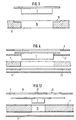
- Fig. 1 shows an IC card with an electronic module 1 in a card body 3 in supervision.
- the card body 3 has dimensions that comply with the ISO standard Designation ISO 7810 are defined.
- the electronic Module 1 is in a defined position in the card body embedded, which is also covered by an ISO standard ISO 7816/2 is specified.
- According to the invention is the card body 3 of the IC card from or off several layers of paper and / or cardboard.
- Fig. 2 shows a multi-layer card structure in cross section before the lamination of the individual card layers.
- the card structure consists of an upper cover layer 5, a core layer 7 and a lower cover layer 9.
- Die Core layer 7 is thermally activated on both sides with a thin Provided adhesive layer 11, with the help of which Layers are glued.
- windows 13 or 15 stamped so that after merging and Glue the three layers into a two-stage recess arises in the card body.
- the windows in the individual core layers from the top cover layer considered getting smaller and smaller.
- Such a map structure is particularly advantageous if the casting compound of electronic module is teardrop-shaped, such as it e.g. is shown in Fig. 9, because then the contours the recess easily adaptable to the shape of the casting compound and the bottom area of the recess is small.
- the production of the card laminate can be done in large throughputs respectively. So layers 5, 7 and 9 of rolls be provided and heated by lamination Laminating rolls are performed, between which the thermally activated adhesive layers can be activated. It an endless laminate is created, which in corresponding Clearances with the cutouts to accommodate the electronic Module is provided. From this endless laminate in a further process step the individual card bodies punched out. In the recess of the card body the electronic modules 1 are glued. The necessary Adhesive can either be located directly on the module or z. B. in the form of a liquid adhesive in the recess be introduced. The installation of the module in the card body is possible before or after the card is punched out.
- the connectivity between the module and the card body can increase instead of above the card layer lying thermo-activatable adhesive 11 the core layer 7 are provided with a fabric 8, which with a thermally activated adhesive is soaked. 2 is the fabric thermo-activated by the points in the top Layer 11 indicated.
- the fabric can be chosen this way be that there is an optimal bond strength between the electronic module and the card body allowed. This is on the finished card Tissue between the cover layer 5 and the core layer 7. Through the firm connection of the module with the tissue the module is between the finished IC card anchored to the card layers.
- the core layer 7 only in the area the window 15 to be provided with a fabric or a film. The effects mentioned above can also be achieved with this.
- the module shown in Fig. 2 carries on its surface 12 contact areas for touching contact removal.
- the IC card can also be used with an electronic one Module are provided for a contactless Data exchange is suitable.
- Such a module can be used in the Window 15 are inserted. In this case, so the window 13 in the cover layer 5 can be dispensed with, so that with the completed IC card, the module for the non-contact data exchange in the window 15 between the cover layers 5 and 9.
- Fig. 3 shows the card body of a single-layer cardboard card in cross section.
- the box 17 can also from a role. In the box are in corresponding distances window 15 punched. Further is by embossing the cardboard 17 in the area of the window 15 creates a recess 19 of shallow depth has a larger diameter than the window 15.
- the resulting recess in the cardboard box can be electronic Module 1 can be glued in, using as an adhesive layer the bottom of the recess 19 is used. The module can again with the help of an adhesive on the module, that as a thermally activated adhesive or as a pressure sensitive adhesive can be formed, or with the help of a liquid adhesive be glued into the recess.
- the card can be in front or punched out of the continuous cardboard after gluing will.
- the IC card When the IC card is finished, it can turn on a part of the back of the card in the module area Window 15 are not filled by the module is. To give the card a better look, you can this part additionally, e.g. B. by casting with a casting compound or closed by other measures will.
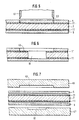
- Layers 5, 7 and 9 are identical to those from FIG. 2.
- the structure still has separate adhesive layers 21 and 23 on that also with appropriate die cuts are provided.
- the adhesive layers 21 and 23 can either be used as thermo-activatable Layers or formed as pressure-sensitive adhesive layers be. In the latter case, the windows in the Layers are created if the layers are still with are coated with a silicone tape in order to glue the Avoid punching tools. After punching the windows the silicone tapes can peel off the adhesive layers rolled up on provided roles.
- the electronic module 1 can even before the roll lamination placed in the window of the adhesive layer 21 in this way that the contact surface area on the adhesive layer 21 rests and the area of the module that the integrated circuit records itself in the window located as shown in the figure.
- laminating of the map layers shown So module simultaneously with the adhesive layer 21 in the Card body recess glued.
- the electronic module is not in the lamination of the card body can be glued into the recess , it is also possible to put the window in the adhesive layer 21 punch out the same size as the window in the top layer 5.
- the shoulder remains the two-tier Clearance when laminating the layers free of the adhesive layer so that when this layer is heated no adhesive material can penetrate the surface of the card can.
- Such an embodiment is particularly advantageous if the punched out card body as an intermediate should be stored.
- the one shown in FIG. 4 Card construction is especially useful for embedding a module for suitable for contactless data exchange. In this Fall can turn on the windows in layers 5 and 21 can be dispensed with.
- FIGS. 5-8 show exemplary embodiments, in which the recess is added later the card body is inserted.
- Fig. 5 shows a card structure consisting of a core layer 7 and the cover layers 5 and 9, the layers by means of thermally activated adhesive layers 11 are connected.
- Can be used as thermally activated adhesive layers e.g. extremely thin polyethylene (PE) film or amorphous Polyethylene terephthalate (APET) film can be used can be applied to the core layer 7 on both sides.
- PE polyethylene
- APET amorphous Polyethylene terephthalate
- the use of a cutting tool to generate the Cutting edge 43 has the advantage that in the visible area the finished chip card a cleaner and optically flawless edge arises, whereas it is in use a milling tool for producing a recess in paper cannot be avoided that it is on the edges "Fraying" occurs, as is shown in FIG Edge area of the lower part of the two-stage recess is indicated.
- a cutting tool and the recess only with a milling tool produce.
- the two-stage recess 19 of the card body is an electronic module, such as it is shown in Fig. 2, introduced and on the Shoulder 45 with the help of those exposed during the milling process thermally activated adhesive layer 11 glued.
- the electronic module additionally to be provided with an adhesive to the composite to improve the card body. Then this is special advantageous if the thermally activated adhesive layers 11 are very thin and the adhesive layer 11 in Shoulder area 45 of the recess is intended during the milling process or inadvertently damaged or eliminated becomes.
- FIG. 7 shows the same layer structure as FIG. 5, however cover layers 5 and 9 are not yet with the core layer 7 connected.
- the card layers with heating stamps 45 and 47 bonded together under the influence of heat and pressure, the heating stamps 45 and 47 in the area in which subsequently created the recess in the card body will have recesses 49 and 51.
- cutouts become when connecting the layers thermally activated layers 11 are not activated, so that no bond between the map layers in this area is created.
- Fig. 8 shows the map structure of Fig. 7, the individual Map layers are now interconnected. Due to the special design of the heating stamp the cover layer 5 with the core layer 7 in the area 53 and the cover layer 9 with the core layer 7 in the region 55 not connected. With the help of the cutting tool 41 can now the upper part of a two-stage recess are generated by first cutting tool 41 inserts at least as far into the card body, that the top layer 5 is severed. The inside of the Part of the cover layer lying on the cut edge can then be cut just remove it because this part is not bonded to the adhesive layer 11 has been received. The lower part of the two-stage recess 19 can be made in an analog manner and Create way with the cutting tool 57. It arises thus a card body, as already shown in FIG.
- the manufacturing method described in connection with FIGS. 7 and 8 is especially for card bodies that consist exclusively of paper and cardboard, suitable since the individual layers of paper do not soften when connecting be like this when laminating plastic layers happens.
- the heating stamp shown the heat is only activated by the paper Adhesive layers passed, which then activated will. So the paper layers themselves stay on the entire manufacturing process is dimensionally stable, so that it is also at the transitions to the unheated areas (see Fig. 7) to no distortion of the paper layers is coming.
- the floor area of the two-tier There is a recess in the finished card body very well trained.
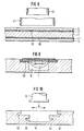
- Fig. 9 shows a single-layer card body with a two-stage recess 19 into which an electronic module 1 is glued with a liquid adhesive 59.
- a liquid adhesive 59 In everyday Use of the chip cards leads to bending loads, on the card body also in the field of electronic Act module. Because of these bending loads it can be in the embodiment shown in FIG. 9 because of the splittability of paper the paper in the shoulder area 45 (see FIG. 6) in the recess 19 directly below the liquid adhesive splits and thereby the electronic module in the course which releases time from the card body.
- a metered amount is in the two-stage recess 19
- Liquid adhesive 59 introduced, which is when the distributed electronic module 1 in the recess 19 so that the undercuts 63 with liquid adhesive 59th are filled (see Fig. 10 and 11). So that's electronic Module 1 anchored in the card body and against Forces acting perpendicular to the card surface are secured.
- the liquid adhesive now offers the entire wall area of the recess wetted, even one good protection against splitting the paper in this area.
- FIG. 12 again shows a multi-layer card body before lamination in cross section.
- the individual layers 5, 7 and 9 are with those shown in FIG Layers identical.
- the upper cover layer 5, however, has instead of window 13, two windows 25 through which a web 27 are separated.
- the electronic module 1 is so in the window 15 of the core layer before lamination 7 inserted, as can be seen in FIG. 12.
- module 1 glued to layer 7 and additionally between the Layers 5 and 7 embedded.
- finished IC card are the contact surfaces of module 1 in the Windows 25 and the embedding between the layers will brought about by the web 27.
- a module for the the above-mentioned manufacturing technique is particularly suitable, is described in detail in EP-B1 0 140 230.
- 13-16 show further embodiments, at which the electronic module by embedding parts of the module between two card layers the manufacture of the card is anchored in the card body.
- Fig. 13 shows a multi-layer card structure consisting from the cover layers 5 and 9 and the core layers 7 and 8.
- the one brought into the map structure shown electronic module 1 has an anchoring frame 65, which protrudes beyond the cast body 67 of the module and that during the production of the cards embedded between the two card layers 5 and 7 becomes.
- the anchor frame is 65 on both sides of thermally activated adhesive layers surrounded so that a good bond between the anchoring frame and the card body emerges.
- the embodiment is the anchoring frame formed as a fabric in the card making Penetrate adhesive material from the adjacent adhesive layers 11 can. This creates an indirect bond of the adjacent adhesive layers 11 and an improved one Anchoring the module in the card body.
- 14-16 show further exemplary embodiments, at which the electronic module between two card layers is embedded.
- the modules point in these figures all have the same structure and are commonly called lead frame modules designated. They consist of a metal plate 69, in which a contact layout is formed and on one side an IC module 71 is applied, which is conductively connected to the contact areas of the contact layout is. The IC chip and the conductive connections are of a protection against mechanical loads Surround the molding compound.
- the anchoring frame is made by extending the contact surfaces formed over the actual contact layout protrude and embedded between two map layers are.
- FIG. 14 shows the same card structure as FIG. 13.
- the anchoring frame is already in production the card, i.e. when connecting the individual layers, cranked into the inside of the card so that the one shown in Fig. 14 shown construction arises. So the production takes place analogous to the manufacture as already in connection was explained with Fig. 12.
- Fig. 15 shows a chip card in cross section, in which the Anchoring frame of the leadframe module is not cranked and the contact surfaces 73 of the electronic module below the map surface.
- the contact areas can in the transition area to the extensions that the Serve anchorage, provided with relief stampings 75 be so that they only have thin webs with the extensions stay connected. This leads to a mechanical Decoupling the transition area module / anchoring frame and thus a relief in this area Bending loads on the card, so that the adhesive layer 11, e.g. B. by tearing or splitting the underlying Card layer 7, not so quickly from this card layer solves.
- FIG. 16 shows the same cross section as FIG. 15.
- the adhesive layer below the anchoring frame 11 leads to the edge area of the lower one Part of the two-stage recess, which creates a Larger adhesive surface for gluing the electronic module is achieved.
- 16 is a heating stamp 77 shown, with the help of which the connection between the anchoring frame and the adhesive layers 11 in one separate station can be improved again.
- FIG. 17 shows a manufacturing method for a paper IC card that consists of two layers, the be connected by means of a pressure sensitive adhesive.
- a first Method step (Fig. 17a) are made with a Silicone tape 29 coated PSA tape 31 composite elements 33 manufactured.
- a further process step electronic modules 1 are made a module band 39 punched out and with the composite element 33 glued.
- the intermediate product shown in Fig. 17c is with a pre-punched cardboard tape 17 with windows 15th merged such that the on the paper layer 35th glued modules come to rest in the windows.
- the completed ones Paper IC cards 3 punched out of the endless belt are also possible.
- the paper card it is also possible to use the paper card to be manufactured individually. In this case, the individual map layers shown in the figures already Card size so that after connecting the individual Layers of the card body in the desired dimensions arises.
- the electronic Modules are preferably placed in a matrix in the box embedded so that finally a multi-use sheet or A multi-purpose web emerges from which individual data carriers punched out with a module.
- the bow can already Provide position markings during manufacture are used to precisely position the punch can be, so that the electronic module after punching positioned exactly to the outer edges of the data carrier is. It is also possible to bow before Punch with a print image so that the Data media already finished after punching out is. Alternatively, it is possible to use electronic Modules for contactless data exchange Multi-purpose sheets on both sides with printed cover layers provided and then punch out the individual data carriers. In this case, the position markers for the punching tool is provided in the printed image of a cover layer be so that on position marks in the Cardboard can be dispensed with.
- FIG. 18 shows a top view of a section of an endless belt, a multi-layer structure, for example 5, shown in cross section.
- the Core layer or layers of the multi-layer card structure included in the area where the punched edge 81 of the card to be punched out, through holes 79.
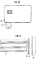
- FIG 20 shows a paper IC card already punched out in FIG At sight.
- the cards either individually or in batches of several at the same time to be edited.
- 21 shows a stack of card bodies 3 in cross section, on the edges of the protective lacquer 85 in the transfer process from the transfer belt 87 using the heating stamp 89 is transmitted.
- edges of the paper cards are then preferably with provide a protective varnish if the cards have a single layer Show card structure, because in this case the methods explained in connection with FIGS. 18 and 19 is not feasible.
- a protective lacquer the protective lacquer being the only one or an additional one Protective measure before splitting the card edge can be.
- the protective lacquer can be colored and as an additional identifier or additional security feature be used.
- IC cards are the layers that make up the top layers form the map
- printed images etc. in whole or in part can be provided
- all common Printing processes such as Embossing, relief printing, offset printing, Steel intaglio printing, screen printing, high pressure, hot stamping printing, Dough printing, wallpaper printing, hectographic printing processes etc. can be used. This can be done by using of art paper that is achievable on paper anyway high print quality can be increased again.
- the printed image can contain certain information (e.g. the credit a new phone card etc.) also in Braille be included, e.g. by embossing or by particularly thick application of paint.
- Individual layers can also be equipped with security elements, such as. a watermark, fragrances, security threads, fluorescent fibers in paper or in Add cards, color capsules in paper fibers, holograms etc. will.
- security elements such as. a watermark, fragrances, security threads, fluorescent fibers in paper or in Add cards, color capsules in paper fibers, holograms etc. will.
Abstract
Description
Die Erfindung betrifft einen ein- oder mehrschichtigen Datenträger mit einem eingebetteten elektronischen Modul, insbesondere Chip-Karten. Desweiteren betrifft die Erfindung ein Herstellungsverfahren für solche Datenträger.The invention relates to a single or multi-layer Data carrier with an embedded electronic module, especially chip cards. The invention further relates to a manufacturing process for such media.
In der Vergangenheit sind verschiedene IC-Karten bekannt geworden, die nach unterschiedlichen Verfahren hergestellt werden.Various IC cards have been known in the past become manufactured by different processes will.
So ist beispielsweise aus der EP-B1 0 140 230 eine IC-Karte bekannt, die aus mehreren Kunststoffschichten aufgebaut ist und in der sogenannten Laminiertechnik hergestellt wird. Dazu wird ein Aufbau, bestehend aus einer oberen Deckschicht, mindestens einer Kernschicht und einer unteren Deckschicht bereitgestellt. Zwischen der oberen Deckschicht und der Kernschicht wird ein elektronisches Modul, bestehend aus einem Substrat, auf dem ein integrierter Schaltkreis mit Kontaktflächen angeordnet ist, plaziert. Dieser Aufbau wird unter der Einwirkung von Wärme und Druck miteinander verbunden, wobei die Kontaktflächen des Moduls in Aussparungen der oberen Deckschicht und der integrierte Schaltkreis in einer Aussparung der Kernfolie zu liegen kommen. Der Verbund der Kunststoffschichten entsteht dadurch, daß die Schichten beim Laminieren erweichen und sich miteinander verbinden. Bei der fertiggestellten Karte ist das Modul zwischen der oberen Deckschicht und der Kernschicht eingebettet.For example, EP-B1 0 140 230 is an IC card known, which is made up of several layers of plastic is and manufactured in the so-called laminating technology becomes. For this, a structure consisting of an upper one Top layer, at least one core layer and a lower layer Cover layer provided. Between the top layer and the core layer becomes an electronic module, consisting of a substrate on which an integrated Circuit with contact surfaces is placed. This structure is under the influence of heat and Pressure connected, the contact surfaces of the Module in recesses of the upper cover layer and the integrated Circuit in a recess in the core film too come to lie. The bond between the plastic layers is created in that the layers soften when laminated and connect with each other. When finished Card is the module between the top layer and embedded in the core layer.
Aus der EP-A1 0 493 738 ist weiterhin eine IC-Karte bekannt, die in der sogenannten Montagetechnik hergestellt wird. Diese Technik zeichnet sich dadurch aus, daß zunächst ein Kartenkörper mit einer mehrstufigen Aussparung bereitgestellt wird. Danach wird das elektronische Modul in die Aussparung eingebracht und verklebt. Dies geschieht bei der EP-A1 0 493 738 mit einem thermoaktivierbaren Kleber. An IC card is also known from EP-A1 0 493 738, which are manufactured in the so-called assembly technology becomes. This technique is characterized in that initially a card body with a multi-level recess provided. After that, the electronic module inserted and glued into the recess. this happens in EP-A1 0 493 738 with a thermally activated adhesive.
Der bereitgestellte Kartenkörper kann z. B. durch Laminieren mehrerer Kunststoffschichten zunächst ohne Aussparung erzeugt werden. In einem weiteren Schritt wird dann die Aussparung z. B. durch Fräsen erzeugt.The card body provided can, for. B. by lamination several layers of plastic initially without recess be generated. In a further step the Recess z. B. generated by milling.
Der Kartenkörper kann aber auch anderweitig hergestellt werden. So ist es beispielsweise aus der DE-A1 41 42 392 bekannt geworden, den Kartenkörper in Spritzgußtechnik zu fertigen. Hierfür wird eine Spritzgußform verwendet, deren Formraum der Form eines Kartenkörpers entspricht. Während des Spritzgußvorganges wird nach nahezu vollständiger Füllung des Formraums die Aussparung im Kartenkörper mit einem beweglichen Stempel erzeugt, der in den Formraum eingefahren werden kann. Nach der Fertigstellung des Kartenkörpers wird in einem zweiten Schritt das elektronische Modul eingeklebt.The card body can also be made otherwise will. For example, it is from DE-A1 41 42 392 become known, the card body in injection molding technology manufacture. An injection mold is used for this, the Form space corresponds to the shape of a card body. While the injection molding process is almost complete the recess in the card body with a Movable stamp created that retracted into the mold space can be. After completing the card body in a second step, the electronic Module glued in.
Alternativ ist es möglich, den beweglichen Stempel direkt dazu zu nutzen, das Modul in die noch nicht erhärtete Kunststoffmasse des Kunststoffkörpers zu drücken. In diesem Fall ist die Herstellung des Kartenkörpers und die Einbettung des Moduls in einem Arbeitsgang abgeschlossen.Alternatively, it is possible to directly move the stamp to use the module in the not yet hardened Press plastic mass of the plastic body. In this Case is the manufacture of the card body and the Embedding of the module completed in one step.
In Spritzgußtechnik hergestellte IC-Karten sind auch aus der EP-B1 0 277 854 bekannt. Dort wird vorgeschlagen, das elektronische Modul bereits während des Einspritzvorgangs der Kunststoffmasse in die Spritzgußform einzulegen. Das Modul wird durch von außen angelegte Saugluft in der Spritzgußform fixiert. Der Gußkörper des Moduls, der den integrierten Schaltkreis schützt, ist schräg geformt und wird so durch das umgebende Spritzgußmaterial sicher im Kartenkörper gehalten.IC cards manufactured by injection molding are also made known from EP-B1 0 277 854. There it is proposed that electronic module already during the injection process insert the plastic mass into the injection mold. The The module is powered by suction air from outside Injection mold fixed. The cast body of the module that the protects integrated circuit, is shaped obliquely and is safely in the surrounding injection molding material Card body held.
Zusätzlich zu den Verfahrensschritten zur Herstellung des Kartenkörpers und zur Einbettung des Moduls gemäß DE-Al 41 42 392 oder EP-B1 0 277 854 sind für die Aufbringung von Druckbildern auf die Kartenoberfläche weitere Maßnahmen vorzusehen. Aus der EP-B1 0 412 893 ist hingegen ein Spritzgußverfahren zur Herstellung von IC-Karten bekannt, bei dem die IC-Karte während des Spritzgießens auch bereits mit einem grafischen Element versehen werden kann. Dazu wird eine kartengroße Papierschicht, die beidseitig bedruckt ist, in die Gußform eingelegt. Danach wird in die Gußform ein transparentes Kunststoffmaterial eingespritzt, so daß bei dem fertiggestellten Kartenkörper das Druckbild von beiden Kartenseiten zu sehen ist. Bei dem Verfahren kann eine Aussparung für das elektronische Modul entweder durch einen in die Gußform ragenden Stempel erzeugt werden, oder aber es kann das Modul direkt in der Gußform fixiert und umspritzt werden.In addition to the process steps for producing the Card body and for embedding the module according to DE-Al 41 42 392 or EP-B1 0 277 854 are for the application further measures of printed images on the card surface to provide. However, EP-B1 0 412 893 describes a Injection molding process for the production of IC cards known where the IC card is already in the process of injection molding can be provided with a graphic element. This is done by a card-sized layer of paper on both sides is printed, inserted into the mold. After that, the Injection molded a transparent plastic material, so that the printed image in the finished card body can be seen from both sides of the map. In the process can be a recess for the electronic module either are generated by a stamp protruding into the mold, or it can be the module directly in the mold fixed and overmolded.
Bei den genannten Verfahren besteht der ein- oder mehrschichtige Kartenkörper aus Kunststoffmaterial. Bei der Laminiertechnik werden die Kartenschichten dabei unter der Einwirkung von Wärme und Druck miteinander verbunden und abschließend wieder abgekühlt. Dafür ist ein relativ hoher Zeitaufwand notwendig. Obwohl derartige Karten im Stapel sogenannter Mehrnutzenbögen "paketweise" hergestellt werden und obwohl das elektronische Modul bei der Verschweißung der Kunststoffschichten bereits miteinlaminiert werden kann, ist der Durchsatz der fertiggestellten Karten pro Zeiteinheit doch stark begrenzt. Diese Begrenzung schlägt sich natürlich auch im Kartenpreis nieder.In the processes mentioned, there is a single or multi-layer Card body made of plastic material. In the The card layers are laminated under the Exposure to heat and pressure combined and finally cooled down again. For that is a relatively high one Time required. Although such cards in the stack so-called multi-use sheets are produced "in packs" and although the electronic module is being welded of the plastic layers are already laminated is the throughput of the completed cards strongly limited per unit of time. This limitation is of course also reflected in the ticket price.
Bei der Spritzgußtechnik ist die Herstellung des Kartenkörpers bzw. der IC-Karte relativ einfach und mit geringerem Zeitaufwand zu realisieren. Die Anlagen für die Fertigung von Spritzgußkörpern bzw. Spritzgußkarten haben jedoch einen hohen Anschaffungspreis. Darüber hinaus sind diese Anlagen vorwiegend für die Einzelkartenfertigung konzipiert, so daß der Durchsatz pro Zeiteinheit in der selben Größenordnung wie bei laminierten Karten bleibt. In the injection molding technique is the manufacture of the card body or the IC card relatively simple and with less Realize time expenditure. The plants for the Manufacture of injection molded articles or injection molded cards however, a high purchase price. Beyond that these systems mainly for single card production designed so that the throughput per unit of time in the remains the same order of magnitude as laminated cards.
Aus dem oben gesagten folgt, daß eine weitere Kostensenkung des Stückpreises einer IC-Karte mit den bisher zur Herstellung der IC-Karte verwendeten Techniken, wenn überhaupt, nur noch in einem geringen Umfang möglich ist.It follows from the above that further cost reduction the unit price of an IC card with the previously available Techniques used to manufacture the IC card, if any, is only possible to a small extent.
Es ist deshalb Aufgabe der Erfindung, eine IC-Karte vorzuschlagen, bei der der Kartenaufbau und das Verfahren zur Herstellung der Karte eine weitere Kostenreduzierung ermöglichen.It is therefore an object of the invention to propose an IC card in which the card structure and the procedure for Production of the card allow a further cost reduction.
Die Aufgabe wird durch die kennzeichnenden Merkmale des Hauptanspruchs gelöst.The task is characterized by the characteristic features of the Main claim solved.
Die Vorteile der Erfindung sind insbesondere darin zu sehen, daß die für den Kartenaufbau benötigten Papierschichten, unabhängig davon, ob es sich bei der Karte um eine Einschicht- oder Mehrschichtkarte handelt, von der Rolle bereitgestellt werden können und die Papier-IC-Karte somit in Endlostechnik zu fertigen ist. Hierbei ist eine Verklebung mehrerer Schichten sehr einfach möglich, da die entweder kalt oder mit Hilfe dünner thermoaktivierbarer Kleber verklebten Schichten ohne aufwendige Wartezeiten gefertigt werden können. Darüber hinaus können sämtliche aus der herkömmlichen Papierverarbeitung bekannten Technologien auf die Herstellung der Papier-IC-Karte übertragen werden, sowohl was die Verbindung der einzelnen Kartenschichten als auch was die Bedruckung der Kartenschichten anbelangt. So können beispielsweise die aus der Papiertechnik bekannten Drucktechniken kostengünstig, z. B. durch Rollen- oder Bogenbedruckung der Schichten eingesetzt werden. Hierbei sind alle aus der Papiertechnik bekannten Druckqualitäten erreichbar. Ferner ist die Papier-IC-Karte im Gegensatz zur Kunststoffkarte umweltschonend und recycelfähig. Ein weiterer Vorteil der IC-Karte ist, daß sie je nach verwendetem Kleber eine hohe Thermostabilität aufweist. Ferner ist die Papier-IC-Karte aufgrund ihrer saugfähigen Oberfläche in einfacher Art und Weise mit individuellen Daten zu versehen, beispielsweise mit einem Tintenstrahldrucker. Schließlich kann die Papier-IC-Karte mit allen Sicherheitsmerkmalen versehen werden, die aus dem Wertpapierbereich bekannt geworden sind. Beispielsweise wäre es möglich, eine der Papierschichten mit einem aus dem Banknotenbereich bekannten Sicherheitsfaden zu versehen und diesen in die Karte zu integrieren.The advantages of the invention can be seen in particular in that the paper layers required for the card structure, regardless of whether the card is one Single-layer or multi-layer cards are about the role can be provided and thus the paper IC card is to be manufactured using endless technology. Here is a bond multiple layers very easily possible because the either cold or with the help of thin thermo-activated Adhesive bonded layers without time-consuming waiting can be manufactured. In addition, all Technologies known from conventional paper processing transferred to the manufacture of the paper IC card be both what the connection of the individual map layers as well as what the printing on the card layers concerned. For example, those from paper technology known printing techniques inexpensively, e.g. B. used by roll or sheet printing of the layers will. Here are all known from paper technology Print quality achievable. Furthermore, the paper IC card in contrast to the plastic card environmentally friendly and recyclable. Another advantage of the IC card is that they have a high thermal stability depending on the adhesive used having. Furthermore, the paper IC card is due their absorbent surface in a simple manner to be provided with individual data, for example with an inkjet printer. Finally, the paper IC card be provided with all security features that have become known from the securities area. For example it would be possible to use one of the layers of paper a security thread known from the area of banknotes to be provided and integrated into the card.
Wie der Stand der Technik belegt, hat sich die gesamte, nunmehr fast 20jährige Entwicklung der IC-Karte an Kunststoff als Material für den Kartenkörper orientiert. Dies ist deswegen unmittelbar verständlich, da mit Kunststoff ein Material ausgewählt worden ist, das sowohl langlebig ist als auch eine hohe Widerstandsfähigkeit aufweist.As the state of the art shows, the entire almost 20 years of development of the IC card on plastic oriented as material for the card body. This is therefore immediately understandable, since with plastic a material has been selected that is both durable is also highly resistant.
Im Laufe der Entwicklung der IC-Karte sind allerdings auch Anwendungen bekannt geworden, bei denen die Karten auch für kürzere Laufzeiten eingesetzt werden. Als Beispiel für eine solche Anwendung sei die Telefonkarte genannt. Es wurde aber auch bei der Wahl für das Kartenmaterial von Telefonkarten der Kunststoff einfach übernommen. Es bestand also offensichtlich ein Vorurteil in der Fachwelt, andere Materialien als Kunststoff für die Herstellung von Karten mit integriertem Schaltkreis überhaupt in Betracht zu ziehen, weil man nur mit diesem Material glaubte, Karten herstellen zu können, die den notwendigen Schutz für den empfindlichen IC-Baustein bieten. Trotz der obengenannten erheblichen Vorteile, die eine Karte aus Papier oder Karton bietet, wurde jedenfalls dieses Material bisher zur Herstellung von Karten mit integriertem Schaltkreisen nicht in Betracht gezogen.However, in the course of the development of the IC card Applications have become known where the cards too can be used for shorter terms. As an example of such an application is called the telephone card. It was also chosen for the map material from Plastic phone cards simply taken over. It consisted so obviously a prejudice in the professional world, materials other than plastic for the manufacture of Integrated circuit cards are even considered draw because you believed only with this material, cards to be able to manufacture the necessary protection for offer the sensitive IC component. Despite the above significant advantages that a paper card or cardboard box, this material has been so far for the production of cards with integrated circuits not considered.
In einem bevorzugten Ausführungsbeispiel der Erfindung wird zunächst ein Papierkartenkörper hergestellt, in den das elektronische Modul später eingeklebt wird. Hierbei kann der Kartenkörper aus mehreren Papierschichten oder aus einer Kartonschicht bestehen. In a preferred embodiment of the invention a paper card body is first produced, in which the electronic module is glued in later. Here the card body can consist of several layers of paper or consist of a layer of cardboard.
In einem weiteren Ausführungsbeispiel der Erfindung wird das elektronische Modul während der Herstellung der Karten in den Kartenkörper einlaminiert. Hierbei kann das Modul entweder zwischen zwei Schichten eingebettet oder aber auch in einer Aussparung eingeklebt werden.In a further embodiment of the invention the electronic module during the production of the cards laminated into the card body. Here, the module either embedded between two layers or else can also be glued into a recess.
In einem weiteren bevorzugten Ausführungsbeispiel wird ein elektronisches Modul, das für einen nichtberührenden Datenaustausch geeignet ist, während des Laminiervorgangs mehrerer Kartenschichten in eine Aussparung der Kernschicht eingebracht.In a further preferred exemplary embodiment, a electronic module for non-contact data exchange is suitable during the lamination process several card layers in a recess in the core layer brought in.
In Zusammenhang mit den nachstehenden Figuren werden Ausführungsbeispiele und weitere Vorteile der Erfindung näher erläutert, darin zeigt:
- Fig. 1
- eine IC-Karte in Aufsicht
- Fig. 2
- einen Querschnitt durch einen Kartenkörperschichtaufbau
- Fig. 3
- einen Querschnitt durch einen Kartenkörper mit einer Aussparung
- Fig. 4
- einen Schichtaufbau für eine in Laminiertechnik herzustellende Karte im Querschnitt
- Fig. 5
- einen Schichtaufbau einer Karte im Querschnitt
- Fig. 6
- den Schichtaufbau aus Fig. 5 im Querschnitt, jedoch mit einer Aussparung
- Fig. 7
- einen Schichtaufbau einer Karte vor dem Verbund der einzelnen Schichten im Querschnitt
- Fig. 8
- den Schichtaufbau aus Fig. 7 im Querschnitt, wobei die Kartenschichten miteinander verbunden sind
- Fig. 9
- eine IC-Karte im Querschnitt
- Fig. 10
- einen Kartenkörper mit Aussparung im Querschnitt
- Fig. 11
- eine IC-Karte im Querschnitt
- Fig. 12
- einen Schichtaufbau für eine in Laminiertechnik herzustellende Karte im Querschnitt
- Fig. 13
- eine IC-Karte im Querschnitt
- Fig. 14
- eine IC-Karte im Querschnitt
- Fig. 15
- eine IC-Karte im Querschnitt
- Fig. 16
- eine IC-Karte im Querschnitt
- Fig. 17
- ein Verfahren zur Herstellung einer IC-Karte
- Fig. 18
- eine mehrschichtiges Endlosband in Aufsicht
- Fig. 19
- einen Querschnitt aus Fig. 18
- Fig. 20
- eine IC-Karte in Aufsicht
- Fig. 21
- einen Stapel von IC-Karten im Querschnitt.
- Fig. 1
- an IC card under supervision
- Fig. 2
- a cross section through a card body layer structure
- Fig. 3
- a cross section through a card body with a recess
- Fig. 4
- a layer structure for a card to be produced in laminating technology in cross section
- Fig. 5
- a layer structure of a card in cross section
- Fig. 6
- 5 in cross section, but with a recess
- Fig. 7
- a layer structure of a card before the composite of the individual layers in cross section
- Fig. 8
- 7 in cross section, the card layers being connected to one another
- Fig. 9
- an IC card in cross section
- Fig. 10
- a card body with a recess in cross section
- Fig. 11
- an IC card in cross section
- Fig. 12
- a layer structure for a card to be produced in laminating technology in cross section
- Fig. 13
- an IC card in cross section
- Fig. 14
- an IC card in cross section
- Fig. 15
- an IC card in cross section
- Fig. 16
- an IC card in cross section
- Fig. 17
- a method of manufacturing an IC card
- Fig. 18
- a multi-layer endless belt under supervision
- Fig. 19
- 18 shows a cross section from FIG. 18
- Fig. 20
- an IC card under supervision
- Fig. 21
- a stack of IC cards in cross section.
Fig. 1 zeigt eine IC-Karte mit einem elektronischen Modul
1 in einem Kartenkörper 3 in Aufsicht. Der Kartenkörper 3
verfügt über Abmessungen, die in einer ISO-Norm mit der
Bezeichung ISO 7810 festgelegt sind. Das elektronische
Modul 1 ist an einer definierten Position in den Kartenkörper
eingebettet, die ebenfalls durch eine ISO-Norm mit
der Bezeichnung ISO 7816/2 festgelegt ist. Erfindungsgemäß
ist der Kartenkörper 3 der IC-Karte aus einer bzw. aus
mehreren Papier- und/oder Kartonschichten hergestellt. Fig. 1 shows an IC card with an
Fig. 2 zeigt einen mehrschichtigen Kartenaufbau im Querschnitt
vor der Laminierung der einzelnen Kartenschichten.
Der Kartenaufbau besteht aus einer oberen Deckschicht 5,
einer Kernschicht 7 und einer unteren Deckschicht 9. Die
Kernschicht 7 ist beidseitig mit einer dünnen thermoaktivierbaren
Klebeschicht 11 versehen, mit Hilfe derer die
Schichten verklebt werden. Vor dem Zusammenführen der einzelnen
Schichten werden in die Schichten 5 und 7 Fenster
13 bzw. 15 eingestanzt, so daß nach dem Zusammenführen und
Verkleben der drei Schichten eine zweistufige Aussparung
in dem Kartenkörper entsteht. Bei der Verwendung mehrerer
Kernschichten ist es auch möglich, im Kartenkörper eine
mehrstufige Aussparung zu erzeugen, wobei die Fenster in
den einzelnen Kernschichten von der oberen Deckschicht
betrachtet immer kleiner werden. Ein solcher Kartenaufbau
ist dann besonders vorteilhaft, wenn die Gußmasse des
elektronischen Moduls tropfenförmig ausgebildet ist, wie
es z.B. in der Fig. 9 gezeigt ist, da dann die Konturen
der Aussparung gut an die Form der Gußmasse anpaßbar und
der Bodenbereich der Aussparung klein ausgebildet ist.Fig. 2 shows a multi-layer card structure in cross section
before the lamination of the individual card layers.
The card structure consists of an
Die Fertigung des Kartenlaminats kann in großen Durchsätzen
erfolgen. So können die Schichten 5, 7 und 9 von Rollen
bereitgestellt werden und zur Laminierung durch geheizte
Laminierrollen geführt werden, zwischen denen die
thermoaktivierbaren Klebeschichten aktiviert werden. Es
entsteht also ein Endloslaminat, das in entsprechenden
Abständen mit den Aussparungen zur Aufnahme des elektronischen
Moduls versehen ist. Aus diesem Endloslaminat werden
in einem weiteren Verfahrensschritt die einzelnen Kartenkörper
ausgestanzt. In die Aussparung des Kartenkörpers
werden die elektronischen Module 1 eingeklebt. Der notwendige
Kleber kann sich entweder am Modul direkt befinden
oder z. B. in Form eines Flüssigklebers in die Aussparung
eingebracht werden. Der Einbau des Moduls in den Kartenkörper
ist vor oder nach dem Ausstanzen der Karte möglich. The production of the card laminate can be done in large throughputs
respectively. So layers 5, 7 and 9 of rolls
be provided and heated by lamination
Laminating rolls are performed, between which the
thermally activated adhesive layers can be activated. It
an endless laminate is created, which in corresponding
Clearances with the cutouts to accommodate the electronic
Module is provided. From this endless laminate
in a further process step the individual card bodies
punched out. In the recess of the card body
the
Um die Verbundfähigkeit zwischen dem Modul und dem Kartenkörper
zu erhöhen, kann anstatt des oberhalb der Kartenschicht
liegenden thermoaktivierbaren Klebers 11 die Kernschicht
7 mit einem Gewebe 8 versehen werden, das mit einem
thermoaktivierbaren Kleber getränkt ist. In der Fig. 2
ist das Gewebe durch die Punkte in der oberen thermoaktivierbaren
Schicht 11 angedeutet. Das Gewebe kann so gewählt
werden, daß es eine optimale Verbundfestigkeit zwischen
dem elektronischem Modul und dem Kartenkörper erlaubt.
Bei der fertiggestellten Karte befindet sich das
Gewebe also zwischen der Deckschicht 5 und der Kernschicht
7. Durch die feste Verbindung des Moduls mit dem Gewebe
ist bei der fertiggestellten IC-Karte das Modul also zwischen
den Kartenschichten verankert. Alternativ zu einem
Gewebe, das sich ganzflächig auf der Kernschicht 7 befindet,
ist auch möglich, die Kernschicht 7 nur im Bereich
des Fensters 15 mit einem Gewebe oder einer Folie zu versehen.
Hiermit sind die obengenannten Effekte auch zu erzielen.The connectivity between the module and the card body
can increase instead of above the card layer
lying thermo-
Das in der Fig. 2 gezeigte Modul trägt auf seiner Oberfläche
12 Kontaktflächen für die berührende Kontaktabnahme.
Alternativ kann die IC-Karte auch mit einem elektronischen
Modul versehen werden, das für einen berührungslosen
Datenaustausch geeignet ist. Ein solches Modul kann in dem
Fenster 15 eingelegt werden. In diesem Fall kann also auf
das Fenster 13 in der Deckschicht 5 verzichtet werden, so
daß bei der fertiggestellten IC-Karte das Modul für den
berührungslosen Datenaustausch in dem Fenster 15 zwischen
den Deckschichten 5 und 9 liegt.The module shown in Fig. 2 carries on its
Fig. 3 zeigt den Kartenkörper einer einschichtigen Kartonkarte
im Querschnitt. Der Karton 17 kann ebenfalls von
einer Rolle bereitgestellt werden. In den Karton werden in
entsprechenden Abständen Fenster 15 eingestanzt. Ferner
wird durch Tiefprägung des Kartons 17 im Bereich des Fensters
15 eine Aussparung 19 geringer Tiefe erzeugt, die
einen größeren Durchmesser als das Fenster 15 aufweist. In
die entstandene Aussparung des Kartons kann das elektronische
Modul 1 eingeklebt werden, wobei als Klebeschicht
der Boden der Aussparung 19 genutzt wird. Das Modul kann
wiederum mit Hilfe eines am Modul befindlichen Klebers,
der als thermoaktivierbarer Kleber oder als Haftkleber
ausgebildet sein kann, oder mit Hilfe eines Flüssigklebers
in die Aussparung eingeklebt werden. Die Karte kann vor
oder nach dem Einkleben aus dem Endloskarton ausgestanzt
werden. Bei der fertiggestellten IC-Karte kann sich auf
der Rückseite der Karte im Modulbereich noch ein Teil des
Fensters 15 befinden, der nicht durch das Modul ausgefüllt
ist. Um der Karte ein besseres Aussehen zu verleihen, kann
dieser Teil noch zusätzlich, z. B. durch Vergießen mit
einer Gußmasse oder durch andere Maßnahmen geschlossen
werden.Fig. 3 shows the card body of a single-layer cardboard card
in cross section. The
Fig. 4 zeigt wiederum einen mehrschichtigen Kartenaufbau
vor dem Laminieren im Querschnitt. Die Schichten 5, 7 und
9 sind identisch mit denen aus der Fig. 2. Zusätzlich zu
diesen Schichten weist der Aufbau noch separate Klebeschichten
21 und 23 auf, die auch mit entsprechenden Stanzungen
versehen sind.4 again shows a multi-layer card structure
before laminating in cross section.
Die Klebeschichten 21 und 23 können entweder als thermoaktivierbare Schichten oder als Haftkleberschichten ausgebildet sein. Im letzteren Fall müssen die Fenster in den Schichten erstellt werden, wenn die Schichten noch mit einem Silikonband beschichtet sind, um ein Verkleben der Stanzwerkzeuge zu vermeiden. Nach dem Stanzen der Fenster können die Silikonbänder von den Haftklebeschichten abund auf bereitgestellte Rollen aufgerollt werden.The adhesive layers 21 and 23 can either be used as thermo-activatable Layers or formed as pressure-sensitive adhesive layers be. In the latter case, the windows in the Layers are created if the layers are still with are coated with a silicone tape in order to glue the Avoid punching tools. After punching the windows the silicone tapes can peel off the adhesive layers rolled up on provided roles.
Das elektronische Modul 1 kann bereits vor der Rollenlaminierung
in die Fenster der Klebeschicht 21 derart eingelegt
werden, daß der Kontaktflächenbereich auf der Klebeschicht
21 aufliegt und der Bereich des Moduls, der den
integrierten Schaltkreis aufnimmt, sich in dem Fenster
befindet, so wie es in der Figur gezeigt ist. Bei dem Laminieren
der gezeigten Kartenschichten wird das gezeigte
Modul also gleichzeitig mit der Klebeschicht 21 in der
Aussparung des Kartenkörpers verklebt.The
Falls das elektronische Modul nicht bei der Laminierung
des Kartenkörpers in die Aussparung eingeklebt werden
soll, ist es auch möglich, das Fenster in der Klebeschicht
21 genau so groß auszustanzen wie das Fenster in der Deckschicht
5. In diesem Fall bleibt die Schulter der zweistufigen
Aussparung beim Laminieren der Schichten frei von
der Kleberschicht, so daß bei der Erwärmung dieser Schicht
kein Klebermaterial auf die Oberfläche der Karte dringen
kann. Eine solche Ausführungsform ist besonders vorteilhaft,
wenn der ausgestanzte Kartenkörper als Zwischenprodukt
gelagert werden soll. Auch der in der Fig. 4 gezeigte
Kartenaufbau ist besonders zur Einbettung eines Moduls für
den berührungslosen Datenaustausch geeignet. In diesem
Fall kann wiederum auf die Fenster in den Schichten 5 und
21 verzichtet werden.If the electronic module is not in the lamination
of the card body can be glued into the recess
, it is also possible to put the window in the adhesive layer
21 punch out the same size as the window in the
Die Fig. 2 und 4 zeigen mehrschichtige Kartenaufbauten, bei denen die einzelnen Schichten bereits vor dem Zusammenfügen über Fenster verfügen, die sich nach dem Zusammenfügen der Schichten zu einer Aussparung im Kartenkörper ergänzen. Im Gegensatz dazu zeigen die Fig. 5-8 Ausführungsbeispiele, bei denen die Aussparung nachträglich in den Kartenkörper eingebracht wird.2 and 4 show multi-layer card structures, where the individual layers are already before joining have windows that appear after merging the layers to a recess in the card body complete. In contrast, FIGS. 5-8 show exemplary embodiments, in which the recess is added later the card body is inserted.
Fig. 5 zeigt einen Kartenaufbau, der aus einer Kernschicht
7 und den Deckschichten 5 und 9 besteht, wobei die Schichten
durch thermoaktivierbare Klebeschichten 11 miteinander
verbunden sind. Als thermoaktivierbare Klebeschichten können
z.B. extrem dünne Polyethylen (PE)-Folie oder amorphe
Polyethylenterephthalat (APET)-Folie verwendet werden, die
beidseitig auf die Kernschicht 7 aufgebracht werden. In
der Deckschicht 5 wird zunächst mit einem Schneidewerkzeug
41 eine Schnittkante 43 erzeugt, die den Rand des ersten
Teils einer zweistufigen Aussparung festgelegt. Danach
wird mit einem Fräswerkzeug in dem Kartenkörper die in der
Fig. 6 gezeigte zweistufige Aussparung 19 derart erzeugt,
daß auf der Schulter 45 die thermoaktivierbare Klebeschicht
11 freigelegt wird.Fig. 5 shows a card structure consisting of a
Die Verwendung eines Schneidwerkzeuges zur Erzeugung der
Schnittkante 43 hat den Vorteil, daß im sichtbaren Bereich
der fertiggestellten Chipkarte ein sauberer und optisch
einwandfreier Rand entsteht, wohingegen es bei der Verwendung
eines Fräswerkzeuges zur Herstellung einer Aussparung
im Papier nicht vermieden werden kann, daß es an den Rändern
zu "Ausfransungen" kommt, so wie es in der Fig. 6 im
Randbereich des unteren Teils der zweistufigen Aussparung
angedeutet ist. Selbstverständlich ist es auch möglich,
auf den Einsatz eines Schneidewerkzeuges zu verzichten und
die Aussparung ausschließlich mit einem Fräswerkzeug zu
erzeugen.The use of a cutting tool to generate the
In die zweistufige Aussparung 19 des Kartenkörpers (siehe
Fig. 6) wird ein elektronisches Modul, wie es beispielsweise
in der Fig. 2 gezeigt ist, eingebracht und auf der
Schulter 45 mit Hilfe der beim Fräsvorgang freigelegten
thermoaktivierbaren Klebeschicht 11 verklebt. Selbstverständlich
ist es auch möglich, das elektronische Modul
zusätzlich mit einem Kleber zu versehen, um den Verbund
zum Kartenkörper zu verbessern. Dies ist dann besonders
vorteilhaft, wenn die thermoaktivierbaren Klebeschichten
11 sehr dünn ausgebildet sind und die Klebeschicht 11 im
Schulterbereich 45 der Aussparung beim Fräsvorgang beabsichtigt
oder unbeabsichtigt beschädigt bzw. beseitigt
wird.In the two-
Fig. 7 zeigt den gleichen Schichtaufbau wie Fig. 5, jedoch
sind die Deckschichten 5 und 9 noch nicht mit der Kernschicht
7 verbunden. In dem gezeigten Ausführungsbeispiel
werden die Kartenschichten mit Heizstempeln 45 und 47
unter der Einwirkung von Wärme und Druck miteinander verbunden,
wobei die Heizstempel 45 und 47 in dem Bereich, in
dem nachträglich die Aussparung im Kartenkörper erzeugt
wird, Aussparungen 49 und 51 aufweisen. Im Bereich dieser
Aussparungen werden also beim Verbinden der Schichten die
thermoaktivierbaren Schichten 11 nicht aktiviert, so daß
in diesem Bereich kein Verbund zwischen den Kartenschichten
erstellt wird.FIG. 7 shows the same layer structure as FIG. 5, however
cover
Fig. 8 zeigt den Kartenaufbau aus Fig. 7, wobei die einzelnen
Kartenschichten nunmehr miteinander verbunden sind.
Durch die spezielle Ausbildung der Heizstempel hat sich
die Deckschicht 5 mit der Kernschicht 7 im Bereich 53 und
die Deckschicht 9 mit der Kernschicht 7 im Bereich 55
nicht miteinander verbunden. Mit Hilfe des Schneidwerkzeuges
41 kann nun der obere Teil einer zweistufigen Aussparung
erzeugt werden, indem man das Schneidwerkzeug 41 zunächst
mindestens so weit in den Kartenkörper einführt,
daß die Deckschicht 5 durchtrennt ist. Der innerhalb der
Schnittkante liegende Teil der Deckschicht läßt sich danach
einfach entfernen, da dieser Teil keinen Verbund mit
der Klebeschicht 11 eingegangen ist. Der untere Teil der
zweistufigen Aussparung 19 läßt sich auf analoge Art und
Weise mit dem Schneidwerkzeug 57 erzeugen. Es entsteht
also ein Kartenkörper, wie er bereits in der Fig. 6 gezeigt
ist, mit einer zweistufigen Aussparung, die jedoch
im gesamten Wandbereich über saubere Schnittkanten verfügt.
Selbstverständlich ist das beschriebene Verfahren
nicht auf die Herstellung einer zweistufigen Aussparung
beschränkt. Vielmehr können in analoger Art und Weise auch
stufenlose bzw. mehrstufige Aussparungen im Kartenkörper
erzeugt werden.Fig. 8 shows the map structure of Fig. 7, the individual
Map layers are now interconnected.
Due to the special design of the heating stamp
the
Das im Zusammenhang mit den Fig. 7 und 8 beschriebene Herstellungsverfahren ist besonders für Kartenkörper, die ausschließlich aus Papier und Karton bestehen, geeignet, da die einzelnen Papierschichten beim Verbinden nicht erweicht werden, wie dies beim Laminieren von Kunststoffschichten geschieht. Mit Hilfe der gezeigten Heizstempel wird die Wärme lediglich durch das Papier zu den thermoaktivierbaren Klebeschichten geleitet, die daraufhin aktiviert werden. Die Papierschichten selbst bleiben also während des gesamten Herstellungsverfahrens formstabil, so daß es auch an den Übergängen zu den nicht beheizten Bereichen (siehe Fig. 7) zu keinerlei Verzerrungen der Papierschichten kommt. Der Bodenbereich der zweistufigen Aussparung ist beim fertiggestellten Kartenkörper somit sehr plan ausgebildet.The manufacturing method described in connection with FIGS. 7 and 8 is especially for card bodies that consist exclusively of paper and cardboard, suitable since the individual layers of paper do not soften when connecting be like this when laminating plastic layers happens. With the help of the heating stamp shown the heat is only activated by the paper Adhesive layers passed, which then activated will. So the paper layers themselves stay on the entire manufacturing process is dimensionally stable, so that it is also at the transitions to the unheated areas (see Fig. 7) to no distortion of the paper layers is coming. The floor area of the two-tier There is a recess in the finished card body very well trained.
Fig. 9 zeigt einen einschichtigen Kartenkörper mit einer
zweistufigen Aussparung 19, in die ein elektronisches Modul
1 mit einem Flüssigkleber 59 eingeklebt ist. Im täglichen
Gebrauch der Chipkarten kommt es zu Biegebelastungen,
die auf den Kartenkörper auch im Bereich des elektronischen
Moduls einwirken. Aufgrund dieser Biegebelastungen
kann es bei dem in der Fig. 9 gezeigten Ausführungsbeispiel
wegen der Spaltbarkeit von Papier dazu kommen, daß
sich das Papier im Schulterbereich 45 (siehe Fig. 6) in
der Aussparung 19 direkt unterhalb des Flüssigklebers
spaltet und sich dadurch das elektronische Modul im Laufe
der Zeit aus dem Kartenkörper löst.Fig. 9 shows a single-layer card body with a
two-
Obwohl Chipkarten aus Papier vorzugsweise für Anwendungen,
bei denen die Karte nur eine kurze Lebensdauer aufzuweisen
braucht, verwendet werden sollen und somit ein Kartenaufbau
wie in Fig. 9 gezeigt an sich langlebig genug ist,
läßt sich der Verbund zwischen dem elektronischen Modul
und dem Kartenkörper dadurch verbessern, daß man die zweistufige
Aussparung 19 mit einem geeigneten Fräswerkzeug 61
mit Hinterschneidungen 63 versieht, so wie es in der Fig.
10 gezeigt ist. Although paper chip cards are preferred for applications,
where the card has a short lifespan
needs to be used and thus a map structure
as shown in Fig. 9 is long enough in itself
can the interconnection between the electronic module
and improve the card body by having the two-
In die zweistufige Aussparung 19 wird eine dosierte Menge
Flüssigkleber 59 eingebracht, die sich beim Einbringen des
elektronischen Moduls 1 in der Aussparung 19 so verteilt,
daß auch die Hinterschneidungen 63 mit Flüssigkleber 59
gefüllt sind (siehe Fig. 10 und 11). Somit ist das elektronische
Modul 1 im Kartenkörper verankert und gegen
senkrecht zur Kartenoberfläche wirkende Kräfte gesichert.
Darüber hinaus bietet der Flüssigkleber, der nunmehr den
gesamten Wandbereich der Aussparung benetzt, auch einen
guten Schutz vor dem Aufspalten des Papiers in diesem Bereich.
Alternativ ist es selbstverständlich auch möglich,
auf die Hinterschneidungen zu verzichten und den Flüssigkleber
so zu dosieren, daß der Wandbereich bei der fertiggestellten
Karte weitgehend bzw. vollständig von ihm benetzt
ist.A metered amount is in the two-
Fig. 12 zeigt wiederum einen mehrschichtigen Kartenkörper
vor der Laminierung im Querschnitt. Die einzelnen Schichten
5, 7 und 9 sind mit den in der Fig. 2 gezeigten
Schichten identisch. Die obere Deckschicht 5 weist jedoch
anstatt des Fensters 13 zwei Fenster 25 auf, die durch
einen Steg 27 getrennt sind. Das elektronische Modul 1
wird vor dem Laminieren so in das Fenster 15 der Kernschicht
7 eingelegt, wie es der Fig. 12 zu entnehmen ist.
Bei der Rollenlaminierung der Schichten wird das Modul 1
mit der Schicht 7 verklebt und zusätzlich zwischen den
Schichten 5 und 7 eingebettet. Bei der fertiggestellten
IC-Karte liegen die Kontakflächen des Moduls 1 in den
Fenstern 25 und die Einbettung zwischen den Schichten wird
durch den Steg 27 herbeigeführt. Ein Modul, das für die
obengenannte Herstellungstechnik besonders geeignet ist,
ist in der EP-B1 0 140 230 genau beschrieben.12 again shows a multi-layer card body
before lamination in cross section. The
Die Fig. 13-16 zeigen weitere Ausführungsbeispiele, bei denen das elektronische Modul durch das Einbetten von Teilen des Moduls zwischen zwei Kartenschichten bereits bei der Herstellung der Karte im Kartenkörper verankert wird. 13-16 show further embodiments, at which the electronic module by embedding parts of the module between two card layers the manufacture of the card is anchored in the card body.
Fig. 13 zeigt einen mehrschichtigen Kartenaufbau, bestehend
aus den Deckschichten 5 und 9 und den Kernschichten 7
und 8. Das in den gezeigten Kartenaufbau eingebrachte
elektronische Modul 1 verfügt über einen Verankerungsrahmen
65, der über den Gußkörper 67 des Moduls hinausragt
und der bereits während der Herstellung der Karten
zwischen den beiden Kartenschichten 5 und 7 eingebettet
wird. Wie in der Fig. 13 gezeigt, ist der Verankerungsrahmen
65 beidseitig von thermoaktivierbaren Klebeschichten
umgeben, so daß ein guter Verbund zwischen dem Verankerungsrahmen
und dem Kartenkörper entsteht. In einem bevorzugten
Ausführungsbeispiel ist der Verankerungsrahmen
als Gewebe ausgebildet, in das bei der Kartenherstellung
Klebematerial aus den angrenzenden Klebeschichten 11 eindringen
kann. Dadurch kommt es zu einem indirekten Verbund
der angrenzenden Klebeschichten 11 und zu einer verbesserten
Verankerung des Moduls im Kartenkörper.Fig. 13 shows a multi-layer card structure consisting
from the cover layers 5 and 9 and the core layers 7
and 8. The one brought into the map structure shown
Die Fig. 14-16 zeigen weitere Ausführungsbeispiele, bei
denen das elektronische Modul zwischen zwei Kartenschichten
eingebettet ist. Die Module weisen in diesen Figuren
alle denselben Aufbau auf und werden allgemein als Lead-frame-Module
bezeichnet. Sie bestehen aus einem Metallplättchen
69, in dem ein Kontaktlayout ausgebildet ist und
auf dessen einer Seite ein IC-Baustein 71 aufgebracht ist,
der leitend mit den Kontaktflächen des Kontaktlayouts verbunden
ist. Der IC-Baustein und die leitenden Verbindungen
sind zum Schutz vor mechanischen Belastungen von einer
Gußmasse umgeben. Bei den gezeigten Ausführungsbeispielen
wird der Verankerungsrahmen durch Verlängerungen der Kontaktflächen
gebildet, die über das eigentliche Kontaktlayout
hinausragen und zwischen zwei Kartenschichten eingebettet
sind.14-16 show further exemplary embodiments, at
which the electronic module between two card layers
is embedded. The modules point in these figures
all have the same structure and are commonly called lead frame modules
designated. They consist of a
Fig. 14 zeigt an sich den gleichen Kartenaufbau wie Fig. 13. Der Verankerungsrahmen wird bereits bei der Herstellung der Karte, also beim Verbinden der einzelnen Schichten, in das Karteninnere gekröpft, so daß der in der Fig. 14 gezeigte Aufbau entsteht. Die Herstellung erfolgt also analog zu der Herstellung, wie sie bereits in Verbindung mit Fig. 12 erläutert wurde.FIG. 14 shows the same card structure as FIG. 13. The anchoring frame is already in production the card, i.e. when connecting the individual layers, cranked into the inside of the card so that the one shown in Fig. 14 shown construction arises. So the production takes place analogous to the manufacture as already in connection was explained with Fig. 12.
Fig. 15 zeigt eine Chipkarte im Querschnitt, bei der der
Verankerungsrahmen des Leadframe-Moduls nicht gekröpft ist
und die Kontaktflächen 73 des elektronischen Moduls unterhalb
der Kartenoberfläche liegen. Die Kontaktflächen können
im Übergangsbereich zu den Verlängerungen, die der
Verankerung dienen, mit Entlastungsstanzungen 75 versehen
werden, so daß sie nur über dünne Stege mit den Verlängerungen
verbunden bleiben. Dies führt zu einer mechanischen
Entkopplung des Übergangsbereiches Modul/Verankerungsrahmen
und somit zu einer Entlastung in diesem Bereich bei
Biegebelastungen der Karte, so daß sich die Klebeschicht
11, z. B. durch Einreißen bzw. Aufspalten der darunterliegenden
Kartenschicht 7, nicht so schnell von dieser Kartenschicht
löst.Fig. 15 shows a chip card in cross section, in which the
Anchoring frame of the leadframe module is not cranked
and the contact surfaces 73 of the electronic module below
the map surface. The contact areas can
in the transition area to the extensions that the
Serve anchorage, provided with
Fig. 16 zeigt an sich denselben Querschnitt wie Fig. 15.
Die unterhalb des Verankerungsrahmens verlaufende Klebeschicht
11 führt jedoch bis an den Randbereich des unteren
Teils der zweistufigen Aussparung heran, wodurch eine
größere Klebefläche zur Verklebung des elektronischen Moduls
erreicht wird. Ferner ist in der Fig. 16 ein Heizstempel
77 gezeigt, mit Hilfe dessen der Verbund zwischen
den Verankerungsrahmen und den Klebeschichten 11 in einer
separaten Station nochmals verbessert werden kann.FIG. 16 shows the same cross section as FIG. 15.
The adhesive layer below the anchoring
Fig. 17 zeigt schließlich ein Herstellungsverfahren für
eine Papier-IC-Karte, die aus zwei Schichten besteht, die
mittels eines Haftklebers verbunden werden. In einem ersten
Verfahrensschritt (Fig. 17a) werden aus einem mit einem
Silikonband 29 beschichteten Haftklebeband 31 Verbundelemente
33 hergestellt. Dies geschieht mit aus der Etikettiertechnik
bekannten Verfahren, die dem Fachmann geläufig
sind und hier nicht näher erläutert zu werden brauchen.
Zusätzlich ist die Erstellung solcher Verbundelemente
aus der DE-OS 41 22 049 bekannt. Das mit den Verbundelementen
33 versehene Silikonband 29 wird mit einer
Papierschicht 35 zusammengeführt, die mit einer Haftkleberschicht
37 versehen ist. Da die Haftung des Verbundelements
an der Haftkleberschicht größer als an der Silikonschicht
ist, läßt sich das Verbundelement auf das Haftkleberband
37 übertragen, so daß sich das in der Fig. 17b gezeigte
Zwischenprodukt ergibt. Bei einem weiteren Verfahrensschritt
(Fig. 17c) werden elektronische Module 1 aus
einem Modulband 39 ausgestanzt und mit dem Verbundelement
33 verklebt. Das in der Fig. 17c gezeigte Zwischenprodukt
wird mit einem vorgestanzten Kartonband 17 mit Fenstern 15
derart zusammengeführt, daß die auf der Papierschicht 35
aufgeklebten Module in den Fenstern zu liegen kommen.
Schließlich werden, wie in Fig. 17e gezeigt, die fertiggestellten
Papier-IC-Karten 3 aus dem Endlosband ausgestanzt.
Selbstverständlich ist es auch möglich, die Papierkarte
einzeln zu fertigen. In diesem Fall weisen die
einzelnen in den Figuren gezeigten Kartenschichten bereits
Kartengröße auf, so daß nach dem Verbinden der einzelnen
Schichten bereits der Kartenkörper in den gewünschten Abmessungen
entsteht.17 shows a manufacturing method for
a paper IC card that consists of two layers, the
be connected by means of a pressure sensitive adhesive. In a first
Method step (Fig. 17a) are made with a
Die bisherigen Ausführungen betreffen durchgehend Ausführungsbeispiele, bei denen bereits fertiggestellte Papier- bzw. Kartonbahnen bereitgestellt oder zusammengeführt werden und dabei oder nachträglich ein elektronisches Modul in den Kartenkörper eingesetzt wird. Alternativ ist es auch möglich, elektronische Module bereits bei der Herstellung des Kartons in diesen einzubringen. Dieses Verfahren kann besonders vorteilhaft bei elektronischen Modulen für den berührungslosen Datenaustausch, z.B. bestehend aus einer ringförmigen Spule und einem integrierten Schaltkreis, der leitend mit der Spule verbunden ist, angewendet werden, da bei diesen Modulen die Anforderungen an die Lagegenauigkeit im fertiggestellten Datenträger niedriger sind, als bei Modulen für den berührenden Datenaustausch. Ferner sind die elektronischen Module für den berührungslosen Datenaustausch allseitig von Karton umgeben und formschlüssig in diesen eingebettet, ohne daß aufwendige Maßnahmen für die Herstellung eines Kanals für die Spule des Moduls ergriffen werden müssen. Die elektronischen Module werden bevorzugt matrixförmig in den Karton eingebettet, so daß schließlich ein Mehrnutzenbogen bzw. eine Mehrnutzenbahn entsteht, aus der einzelne Datenträger mit einem Modul ausgestanzt werden. Der Bogen kann bereits bei der Herstellung mit Positionsmarkierungen versehen werden, anhand derer das Stanzwerkzeug exakt positioniert werden kann, so daß das elektronische Modul nach dem Ausstanzen lagegenau zu den Außenkanten des Datenträgers positioniert ist. Es ist ferner möglich, den Bogen vor dem Ausstanzen mit einem Druckbild zu versehen, so daß der Datenträger bereits nach dem Ausstanzen fertiggestellt ist. Alternativ ist es möglich, den mit elektronischen Modulen für den berührungslosen Datenaustausch versehenen Mehrnutzenbogen beidseitig mit bedruckten Deckschichten zu versehen und die einzelnen Datenträger danach auszustanzen. In diesem Fall können die Positionsmarkierungen für das Stanzwerkzeug in dem Druckbild einer Deckschicht vorgesehen werden, so daß auf Positionsmarkierungen in dem Karton verzichtet werden kann.The previous statements consist of exemplary embodiments, where already completed paper or cardboard sheets are provided or merged and with or afterwards an electronic module is inserted into the card body. Alternatively it is also possible to manufacture electronic modules already of the cardboard in this. This method can be particularly advantageous for electronic modules for contactless data exchange, e.g. existing from an annular coil and an integrated Circuit, which is conductively connected to the coil, applied because the requirements for these modules the positional accuracy in the finished data carrier are lower than for modules for touching data exchange. Furthermore, the electronic modules for the Non-contact data exchange surrounded by cardboard on all sides and embedded in a form-fitting manner without the need for complex Measures for the creation of a channel for the Coil of the module must be gripped. The electronic Modules are preferably placed in a matrix in the box embedded so that finally a multi-use sheet or A multi-purpose web emerges from which individual data carriers punched out with a module. The bow can already Provide position markings during manufacture are used to precisely position the punch can be, so that the electronic module after punching positioned exactly to the outer edges of the data carrier is. It is also possible to bow before Punch with a print image so that the Data media already finished after punching out is. Alternatively, it is possible to use electronic Modules for contactless data exchange Multi-purpose sheets on both sides with printed cover layers provided and then punch out the individual data carriers. In this case, the position markers for the punching tool is provided in the printed image of a cover layer be so that on position marks in the Cardboard can be dispensed with.
Es können unterschiedliche Maßnahmen ergriffen werden, die im Zusammenhang mit den Fig. 18-21 erläutert werden, um ein Aufspalten des Papiers oder des Kartons im Randbereich der ausgestanzten Papier-IC-Karten zu verhindern.Different measures can be taken are explained in connection with FIGS. 18-21 splitting the paper or cardboard in the edge area to prevent the punched-out paper IC cards.
Fig. 18 zeigt in Aufsicht einen Ausschnitt aus einem Endlosband,
das einen mehrschichtigen Aufbau, beispielsweise
den in der Fig. 5 im Querschnitt gezeigten, aufweist. Die
Kernschicht bzw. Kernschichten des mehrschichtigen Kartenaufbaus
enthalten in dem Bereich, in dem die Stanzkante 81
der auszustanzenden Karte liegt, Durchgangslöcher 79. 18 shows a top view of a section of an endless belt,
a multi-layer structure, for example
5, shown in cross section. The
Core layer or layers of the multi-layer card structure
included in the area where the punched
Fig. 19 zeigt einen Querschnitt entlang der Linie A-A der
Fig. 18. Beim Verbinden der einzelnen Kartenschichten
dringt Material aus den angrenzenden thermoaktivierbaren
Klebeschichten 11 in die Durchgangslöcher ein, so daß die
Deckschichten 5 und 9 indirekt miteinander verbunden werden.
Stanzt man nunmehr die Karte entlang der Stanzkante
81 derart aus, daß zumindest noch ein Teil eines jeden
Durchgangsloches 79 im Kartenkörper liegt, so wie es in
den Fig. 18 und 19 angedeutet ist, so erhält man einen
Kartenrand, der im Kernbereich abwechselnd aus Papier bzw.
Karton und Klebematerial aus den Klebeschichten besteht.
Einem Aufspalten der Kernschicht kann somit weitgehend
vorgebeugt werden.19 shows a cross section along the line A-A of FIG
Fig. 18. When connecting the individual card layers
penetrates material from the adjacent thermo-activated
Fig. 20 zeigt eine bereits ausgestanzte Papier-IC-Karte in
Aufsicht. Um den Rand der Karte vor Aufspalten zu schützen,
wird auf diese ein spezieller Schutzlack 85 mit einem
Auftragswerk 83 aufgetragen. Hierbei können die Karten
entweder einzeln oder im Stapel zu mehreren gleichzeitig
bearbeitet werden.20 shows a paper IC card already punched out in FIG
At sight. To protect the edge of the card from splitting,
a special
Fig. 21 zeigt einen Stapel aus Kartenkörpern 3 im Querschnitt,
auf deren Ränder der Schutzlack 85 im Transferverfahren
vom Transferband 87 mit Hilfe des Heizstempels
89 übertragen wird.21 shows a stack of
Vorzugsweise werden die Ränder der Papierkarten dann mit einem Schutzlack versehen, wenn die Karten einen einschichtigen Kartenaufbau aufweisen, da in diesem Fall das in Verbindung mit den Fig. 18 und 19 erläuterte Verfahren nicht durchführbar ist. Selbstverständlich können auch mehrschichtige Karten mit einem Schutzlack versehen werden, wobei der Schutzlack die einzige oder aber eine zusätzliche Schutzmaßnahme vor dem Aufspalten des Kartenrandes sein kann. Der Schutzlack kann farbig ausgebildet sein und als zusätzliche Kennung bzw. zusätzliches Sicherheitsmerkmal verwendet werden. The edges of the paper cards are then preferably with provide a protective varnish if the cards have a single layer Show card structure, because in this case the methods explained in connection with FIGS. 18 and 19 is not feasible. Of course you can too multi-layer cards are provided with a protective lacquer, the protective lacquer being the only one or an additional one Protective measure before splitting the card edge can be. The protective lacquer can be colored and as an additional identifier or additional security feature be used.
Abschließend sei erwähnt, daß bereits vor der Erstellung der IC-Karten diejenigen Schichten, die die Deckschichten der Karte bilden, mit Druckbildern etc. ganz oder bereichsweise versehen werden können, wobei alle gängigen Druckverfahren, wie z.B. Prägedruck, Reliefdruck, Offsetdruck, Stahltiefdruck, Siebdruck, Hochdruck, Heißprägedruck, Teigdruck, Tapetendruck, hektografische Druckverfahren etc. verwendbar sind. Hierbei kann durch die Verwendung von Kunstdruckpapier die auf Papier ohnehin erzielbare hohe Druckqualität nochmals erhöht werden. In das Druckbild können bestimmte Informationen (z.B. das Guthaben einer neuwertigen Telefonkarte etc.) auch in Blindenschrift aufgenommen werden, z.B. durch Prägung bzw. durch besonders dicken Farbauftrag. Bei der fertiggestellten Karte können die außenliegenden Oberflächen der Deckschichten durch eine dünne Lackschicht, bestehend z.B. aus Nitrolack, Kalanderlack, UV-härtendem Lack, elektronenstrahlhärtendem Lack etc. geschützt sein. Der Lack kann in Form einer Glanzlackierung bzw. einer Mattlackierung aufgebracht werden. Ferner ist es möglich, die Lackschichten zu grainieren.Finally, it should be mentioned that before the creation the IC cards are the layers that make up the top layers form the map, with printed images etc. in whole or in part can be provided, all common Printing processes such as Embossing, relief printing, offset printing, Steel intaglio printing, screen printing, high pressure, hot stamping printing, Dough printing, wallpaper printing, hectographic printing processes etc. can be used. This can be done by using of art paper that is achievable on paper anyway high print quality can be increased again. In the The printed image can contain certain information (e.g. the credit a new phone card etc.) also in Braille be included, e.g. by embossing or by particularly thick application of paint. When finished Can map the outer surfaces of the face layers through a thin layer of lacquer, e.g. out Nitro lacquer, calender lacquer, UV-hardening lacquer, electron-beam hardening lacquer Paint etc. must be protected. The paint can be in In the form of a gloss or matt coating applied will. It is also possible to apply the layers of paint to grain.
Einzelne Schichten können zusätzlich auch mit Sicherheitselementen, wie z.B. einem Wasserzeichen, Duftstoffen, Sicherheitsfäden, fluoreszierenden Fasern in Papier bzw. in Karten, Farbkapseln in Papierfasern, Hologrammen etc. versehen werden.Individual layers can also be equipped with security elements, such as. a watermark, fragrances, security threads, fluorescent fibers in paper or in Add cards, color capsules in paper fibers, holograms etc. will.
Auch das Aufbringen sonstiger Elemente, wie z.B. eine Magnetpiste durch das Auftragen eines Magnetlackes auf Wasserbasis oder einer Zündholzreibfläche, ist bei Papierkarten besonders einfach.The application of other elements, such as a magnetic track by applying a water-based magnetic varnish or a matchstick surface is for paper cards particularly easy.
Schließlich können in die dickeren Papierschichten bzw. Kartonschichten bei der Herstellung dieser Schichten Fäden eingearbeitet werden, die diese Schichten schwieriger spaltbar machen. Entsprechende Techniken sind aus der Papierverarbeitung bekannt und sollen hier nicht näher erläutert werden. Zur Verbindung der einzelnen Papier- oder Kartonschichten können neben theromoaktivierbaren Klebern, auch Haftkleber oder Flüssigkleber eingesetzt werden. Um einem Aufspalten des Papiers oder Kartons im Bereich der Aussparung für das Modul vorzubeugen, können diese Bereiche durch Gewebe, Flüssigkleber oder Harze verfestigt werden.Finally, the thicker layers of paper or Cardboard layers in the manufacture of these layers of threads are incorporated which make these layers more difficult make fissile. Appropriate techniques are from paper processing known and should not be explained here will. To connect the individual paper or Cardboard layers can, in addition to thermally activated adhesives, pressure sensitive adhesives or liquid adhesives can also be used. Around splitting the paper or cardboard in the area of the These areas can prevent recesses for the module solidified by tissue, liquid glue or resins will.
Claims (29)
- A one- or multilayer data carrier designed as an IC card and having an embedded electronic module (1) to be used for exchanging data with an external device, characterized in that the data carrier consists of paper and/or cardboard.
- The data carrier of claim 1, characterized in that it consists of a card body (3) with a gap in which the electronic module (1) is embedded, and the dimensions of the card body (3) fulfill the ISO standard ISO 7810.
- The data carrier of claims 1 to 2, characterized in that the embedded electronic module (1) has contact surfaces (73) for touch contact, and the contact surfaces (73) are located in an area of the data carrier fixed by the ISO standard ISO 7816/2.
- The data carrier of one or more of claims 2 to 3, characterized in that the card body (3) is formed from single-layer cardboard (17) containing a gap for receiving the electronic module (1).
- The data carrier of claim 4, characterized in that the surfaces of the cardboard (17) are provided with a surface coating and with a printed image.
- The data carrier of one or more of claims 2 to 3, characterized in that it has a plurality of layers, at least the layers (7, 21, 23) located between the cover layers (5, 9) of the card body (3) being provided with windows (15) for receiving the electronic module (1).
- The data carrier of claim 6, characterized in that the layers (5, 7, 9) are interconnected by adhesive layers (11, 21, 23) formed either as thermally activable layers or as contact adhesive layers.
- The data carrier of claim 6, characterized in that an electronic module (1) for noncontacting communication is embedded in the windows (15) in the middle layers (7, 21, 23) located between the cover layers.
- The data carrier of claims 6 to 7, characterized in that at least one of the cover layers (5, 9) is provided with a window (13) so that a two-step gap in which an electronic module (1) for contacting communication is embedded is formed in the card body (3) along with the windows (15) in the middle layers (7, 21, 23).
- The data carrier of claim 6, characterized in that the cover layers (5, 9) are provided with a surface coating and a printed image.
- The data carrier of any of claims 2 to 10, characterized in that the electronic module (1) is glued into the gap with a liquid adhesive (59).
- The data carrier of claim 11, characterized in that the liquid adhesive (59) moistens at least largely the entire wall area of the gap so as to prevent splitting of the card layers in this area.
- The data carrier of one of claims 11 to 12, characterized in that the gap is provided with at least one undercut (63) filled with liquid adhesive (59).
- The data carrier of claim 9, characterized in that the adhesive layer (11) connecting the cover layer (5) with the middle layers (7) is exposed in the shoulder area (45) of the two-step gap and serves to connect the electronic module (1) with the card body (3).
- The data carrier of one of claims 6 to 7, characterized in that the electronic module (1) has an anchoring frame (65) located between two layers of the card body (3).
- The data carrier of claim 15, characterized in that the layers adjacent the anchoring frame (65) are adhesive layers.
- A method for producing the data carrier, in particular IC card, of claim 1, characterized by the steps ofsupplying cardboard (17) with the thickness of the data carrier from a roll in endless form,providing the cardboard (17) with punchings at predetermined intervals so that windows (15) arise in the cardboard (17),providing the cardboard (17) with debossing in the area of the windows (15) so that depressions (19) with a greater diameter than that of the windows (15) arise in the cardboard (17) in the area of the windows (15),inserting electronic modules (1) in the resulting gaps in the cardboard (17), whereby a first area of the module (1) bearing contact surfaces (73) for contacting coupling is located in the depression (19) and a second area of the module (1) bearing an integrated circuit is located in the window (15),gluing the modules in the gaps,punching individual data carriers out of the roll.
- A method for producing the data carrier, in particular IC card, of claim 1, characterized by the steps ofsupplying an upper cover layer (5), a lower cover layer (9) and at least one core layer (7) of cardboard and/or paper each from a roll,punching windows (15) in the core layer (7) at predetermined intervals,bringing the core layer (7) and the lower cover layer (9) together and gluing them, whereby gaps arise in the core layer (7) at the positions of the windows (15),introducing an electronic module (1) for noncontacting communication in the resulting gaps,bringing the core layer (7) together with the upper cover layer (5) and gluing them, andpunching individual data carriers out of the resulting band.
- A method for producing the data carrier, in particular IC card, of claim 1, characterized by the steps ofsupplying an upper cover layer (5), a lower cover layer (9) and at least one core layer (7) of cardboard and/or paper each from a roll,providing the core layer (7) and the upper cover layer (5) with windows (13, 15) by punching, the openings in the cover layer (5) being greater than the openings in the core layer (7),interconnecting the three layers (5, 7, 9), yielding a band having two-step gaps at predetermined intervals,introducing electronic modules (1) in the two-step gaps, whereby a part of the electronic module (1) bearing contact surfaces (73) for contacting communication is located in the upper area of the gap and a part of the electronic module (1) receiving an integrated circuit is located in the lower area of the gap,punching individual data carriers out of the resulting band.
- A method for producing the data carrier, in particular IC card, of claim 1, characterized by the steps ofsupplying an upper layer (5), a lower layer (9) and at least one core layer (7) of cardboard and/or paper,interconnecting the layers, yielding a band or sheet,cutting in at least the upper cover layer (5) with a cutting tool (41) at predetermined intervals in such a way that the edge of cut (43) includes a certain area,using a milling tool to produce a gap in said area, whereby the limit of the gap located in the upper cover layer (5) is fixed by the edge of cut (43),introducing electronic modules (1) in the resulting gaps,punching individual data carriers out of the resulting band or sheet.
- A method for producing the data carrier of claim 1, characterized in that one produces cardboard (17) having the card thickness, and already embeds the electronic module (1) in the cardboard (17) during production of the cardboard.
- A method for producing the data carrier of claim 1, characterized in that one produces cardboard (17) in which the electronic module (1) is already embedded during production, and provides the cardboard (17) with at least one cover layer (5).
- The method of one of claims 21 to 22, characterized in that the cardboard (17) is produced as a multiple-copy sheet or multiple-copy web in which a plurality of electronic modules (1) are incorporated in a matrix arrangement, and individual data carriers are punched out of the multiple-copy web in such a way that each data carrier contains at least one electronic module (1).
- The method of any of claims 21 to 23, characterized in that electronic modules (1) for noncontacting data exchange are embedded in the cardboard (1), being surrounded by the cardboard (17) positively and on all sides.
- The method of claim 19, characterized in that the modules (1) are inserted in the card structure before connection of the individual layers, and are glued directly in the resulting gaps during connection of the layers.
- The method of claim 19, characterized in that the modules are glued into the gaps after connection of the individual layers.
- The method of any of claims 18 to 20, characterized in that the individual layers are interconnected by thermally activable adhesive layers (11) which are activated by heated laminating rolls.
- The method of any of claims 18 to 20, characterized in that the individual layers are interconnected by contact adhesive.
- The method of claim 27, characterized in thatat least a part of the core layers (7) has through holes (79) which are filled with adhesive from the thermally activable adhesive layers (11) during connection of the card layers so that the layers adjacent said core layers (7) are interconnected indirectly via the adhesive in the through holes (79),the through holes (79) are located in the area of the punching edges (81) along which the individual cards are punched out in a further step, andthe individual cards are punched out of the resulting sheet or band in such a way that the punching edge (81) extends through the through holes (79) in said core layers (7).
Applications Claiming Priority (3)
| Application Number | Priority Date | Filing Date | Title |
|---|---|---|---|
| DE4403513 | 1994-02-04 | ||
| DE4403513A DE4403513A1 (en) | 1994-02-04 | 1994-02-04 | Chip card with an electronic module and method for producing such a chip card |
| PCT/EP1995/000397 WO1995021423A1 (en) | 1994-02-04 | 1995-02-03 | Data carrier with an electronic module and process for producing the same |
Publications (3)
| Publication Number | Publication Date |
|---|---|
| EP0742926A1 EP0742926A1 (en) | 1996-11-20 |
| EP0742926B1 true EP0742926B1 (en) | 1998-07-08 |
| EP0742926B2 EP0742926B2 (en) | 2007-06-27 |
Family
ID=6509509
Family Applications (1)
| Application Number | Title | Priority Date | Filing Date |
|---|---|---|---|
| EP95909671A Expired - Lifetime EP0742926B2 (en) | 1994-02-04 | 1995-02-03 | Data carrier with an electronic module and process for producing the same |
Country Status (14)
| Country | Link |
|---|---|
| US (1) | US5888624A (en) |
| EP (1) | EP0742926B2 (en) |
| JP (1) | JPH09508330A (en) |
| KR (1) | KR100408842B1 (en) |
| CN (1) | CN1098506C (en) |
| AT (1) | ATE168206T1 (en) |
| AU (1) | AU1807395A (en) |
| CA (1) | CA2182705C (en) |
| DE (3) | DE9422424U1 (en) |
| DK (1) | DK0742926T4 (en) |
| ES (1) | ES2117854T5 (en) |
| MX (1) | MX9603163A (en) |
| RU (1) | RU2169389C2 (en) |
| WO (1) | WO1995021423A1 (en) |
Cited By (1)
| Publication number | Priority date | Publication date | Assignee | Title |
|---|---|---|---|---|
| DE102013002536A1 (en) | 2013-02-14 | 2014-08-14 | Colorplast Ag | Method for producing a paper carrier card with detachable integrated chip module card and paper carrier card made of paper with detachable integrated chip module card |
Families Citing this family (110)
| Publication number | Priority date | Publication date | Assignee | Title |
|---|---|---|---|---|
| DE19512725C1 (en) * | 1995-04-05 | 1996-09-12 | Orga Kartensysteme Gmbh | ID card or the like in the form of a chip card |
| DE19534480C2 (en) * | 1995-09-18 | 1999-11-11 | David Finn | IC card module for the production of an IC card and IC card with an IC card module |
| GB2309933B (en) * | 1996-02-12 | 2000-02-23 | Plessey Telecomm | Contact card |
| FR2749687B1 (en) * | 1996-06-07 | 1998-07-17 | Solaic Sa | MEMORY CARD AND METHOD FOR MANUFACTURING SUCH A CARD |
| JPH09327990A (en) * | 1996-06-11 | 1997-12-22 | Toshiba Corp | Card type storing device |
| DE19632117C1 (en) * | 1996-08-08 | 1997-12-18 | Siemens Ag | Chip card for use with read/write station |
| DE19708617C2 (en) * | 1997-03-03 | 1999-02-04 | Siemens Ag | Chip card module and method for its production as well as this comprehensive chip card |
| DE19710144C2 (en) * | 1997-03-13 | 1999-10-14 | Orga Kartensysteme Gmbh | Method for producing a chip card and chip card produced according to the method |
| DE19721058A1 (en) * | 1997-05-20 | 1998-11-26 | Giesecke & Devrient Gmbh | Injection molded card with decorative layer |
| EP0905657B1 (en) | 1997-09-23 | 2003-05-28 | STMicroelectronics S.r.l. | Currency note comprising an integrated circuit |
| NL1008929C2 (en) * | 1998-04-20 | 1999-10-21 | Vhp Ugchelen Bv | Substrate made of paper provided with an integrated circuit. |
| TW484101B (en) * | 1998-12-17 | 2002-04-21 | Hitachi Ltd | Semiconductor device and its manufacturing method |
| FR2796183B1 (en) * | 1999-07-07 | 2001-09-28 | A S K | CONTACTLESS ACCESS TICKET AND MANUFACTURING METHOD THEREOF |
| DE19935170A1 (en) * | 1999-07-28 | 2001-02-01 | Koenig & Bauer Ag | Refinement processes |
| FR2801708B1 (en) | 1999-11-29 | 2003-12-26 | A S K | METHOD OF MANUFACTURING A CONTACTLESS CHIP CARD WITH AN ANTENNA SUPPORT OF FIBROUS MATERIAL |
| FR2801709B1 (en) * | 1999-11-29 | 2002-02-15 | A S K | CONTACTLESS OR CONTACT-FREE HYBRID CHIP CARD TO REDUCE THE RISK OF FRAUD |
| FR2801707B1 (en) | 1999-11-29 | 2002-02-15 | A S K | METHOD FOR MANUFACTURING A CONTACT-FREE CONTACT HYBRID CHIP CARD WITH AN ANTENNA SUPPORT OF FIBROUS MATERIAL |
| DE10016715C1 (en) * | 2000-04-04 | 2001-09-06 | Infineon Technologies Ag | Laminated smart card arrangement e.g. for telephone card |
| DE10032128A1 (en) * | 2000-07-05 | 2002-01-17 | Giesecke & Devrient Gmbh | Security paper and value document made from it |
| US6533181B1 (en) * | 2000-07-22 | 2003-03-18 | Roboric Vision Systems, Inc. | Direct marking of parts with encoded symbology method, apparatus and symbolody |
| JP2002092577A (en) * | 2000-09-20 | 2002-03-29 | Hitachi Maxell Ltd | Combination card and manufacturing method thereof |
| US6923378B2 (en) * | 2000-12-22 | 2005-08-02 | Digimarc Id Systems | Identification card |
| FR2826154B1 (en) * | 2001-06-14 | 2004-07-23 | A S K | CHIP CARD WITHOUT CONTACT WITH AN ANTENNA SUPPORT AND CHIP SUPPORT OF FIBROUS MATERIAL |
| DE10139395A1 (en) * | 2001-08-10 | 2003-03-06 | Infineon Technologies Ag | Contacting of semiconductor chips in chip cards |
| JP2003085525A (en) * | 2001-09-13 | 2003-03-20 | Konica Corp | Ic card, and card authentication method |
| FR2829857B1 (en) * | 2001-09-14 | 2004-09-17 | A S K | CONTACTLESS OR HYBRID CONTACT-CONTACTLESS CHIP CARD WITH REINFORCED HOLDING OF THE ELECTRONIC MODULE |
| RU2300159C2 (en) * | 2001-09-18 | 2007-05-27 | Награид Са | Method for producing cards or electronic labels |
| JPWO2003034103A1 (en) * | 2001-10-12 | 2005-02-03 | ダイセル化学工業株式会社 | Light control sheet and manufacturing method thereof |
| CA2470094C (en) | 2001-12-18 | 2007-12-04 | Digimarc Id Systems, Llc | Multiple image security features for identification documents and methods of making same |
| US7694887B2 (en) | 2001-12-24 | 2010-04-13 | L-1 Secure Credentialing, Inc. | Optically variable personalized indicia for identification documents |
| US20030211296A1 (en) * | 2002-05-10 | 2003-11-13 | Robert Jones | Identification card printed with jet inks and systems and methods of making same |
| CA2471457C (en) | 2001-12-24 | 2011-08-02 | Digimarc Id Systems, Llc | Covert variable information on id documents and methods of making same |
| CA2470600C (en) | 2001-12-24 | 2009-12-22 | Digimarc Id Systems, Llc | Systems, compositions, and methods for full color laser engraving of id documents |
| US7728048B2 (en) | 2002-12-20 | 2010-06-01 | L-1 Secure Credentialing, Inc. | Increasing thermal conductivity of host polymer used with laser engraving methods and compositions |
| EP1467834A4 (en) | 2001-12-24 | 2005-04-06 | Digimarc Id Systems Llc | Laser etched security features for identification documents and methods of making same |
| WO2003056499A2 (en) * | 2001-12-24 | 2003-07-10 | Digimarc Id Systems Llc | Pet based multi-multi-layer smart cards |
| JP3645222B2 (en) * | 2002-01-22 | 2005-05-11 | 日立電子サービス株式会社 | ID photo with ID chip |
| WO2003088144A2 (en) | 2002-04-09 | 2003-10-23 | Digimarc Id Systems, Llc | Image processing techniques for printing identification cards and documents |
| US6851617B2 (en) * | 2002-04-19 | 2005-02-08 | Avery Dennison Corporation | Laser imageable RFID label/tag |
| US7824029B2 (en) | 2002-05-10 | 2010-11-02 | L-1 Secure Credentialing, Inc. | Identification card printer-assembler for over the counter card issuing |
| DE10232568A1 (en) * | 2002-07-18 | 2004-01-29 | Agfa-Gevaert Ag | identity card |
| US6910635B1 (en) * | 2002-10-08 | 2005-06-28 | Amkor Technology, Inc. | Die down multi-media card and method of making same |
| US7540426B1 (en) * | 2002-11-07 | 2009-06-02 | American Express Travel Related Services Company, Inc. | Foldable transaction cards and methods of making the same |
| US7804982B2 (en) | 2002-11-26 | 2010-09-28 | L-1 Secure Credentialing, Inc. | Systems and methods for managing and detecting fraud in image databases used with identification documents |
| JP2004185208A (en) * | 2002-12-02 | 2004-07-02 | Sony Corp | Ic card |
| DE10304824A1 (en) * | 2003-01-31 | 2004-08-12 | Varta Microbattery Gmbh | Thin electronic chip card |
| DE602004030434D1 (en) | 2003-04-16 | 2011-01-20 | L 1 Secure Credentialing Inc | THREE-DIMENSIONAL DATA STORAGE |
| DE10356153B4 (en) | 2003-12-02 | 2010-01-14 | Infineon Technologies Ag | Module for contactless chip cards or identification systems |
| US7631812B2 (en) | 2003-12-10 | 2009-12-15 | Williams Troy P | Foldable transaction card systems |
| US7721956B2 (en) | 2003-12-10 | 2010-05-25 | American Express Travel Related Services Company, Inc. | Foldable transaction card systems |
| DE102004011702B4 (en) | 2004-03-10 | 2006-02-16 | Circle Smart Card Ag | Method for producing a card body for a contactless chip card |
| US7744002B2 (en) * | 2004-03-11 | 2010-06-29 | L-1 Secure Credentialing, Inc. | Tamper evident adhesive and identification document including same |
| DE202004003701U1 (en) * | 2004-03-12 | 2004-08-12 | Cubit Electronics Gmbh | Flat transponder |
| DE102004018081A1 (en) | 2004-04-08 | 2005-10-27 | Giesecke & Devrient Gmbh | security paper |
| FR2868987B1 (en) | 2004-04-14 | 2007-02-16 | Arjo Wiggins Secutity Sas Soc | STRUCTURE COMPRISING AN ELECTRONIC DEVICE, IN PARTICULAR FOR THE MANUFACTURE OF A SECURITY OR VALUE DOCUMENT |
| KR100602621B1 (en) * | 2004-06-16 | 2006-07-19 | 한국조폐공사 | A Prefabricated Combi-card and method for making the same |
| PL1756755T3 (en) * | 2004-06-16 | 2012-08-31 | Gemalto Sa | Shielded contactless electronic document |
| FR2877461B1 (en) | 2004-11-02 | 2007-05-18 | Gemplus Sa | PERSONALIZED ELECTRONIC DEVICE OF THE USB KEY TYPE AND METHOD OF MANUFACTURING SUCH A DEVICE |
| EP1835796B9 (en) | 2004-12-03 | 2011-02-23 | Hallys Corporation | Interposer bonding device |
| US20060146271A1 (en) * | 2005-01-04 | 2006-07-06 | Pennaz Thomas J | Universal display module |
| EP1876877B1 (en) | 2005-04-06 | 2010-08-25 | Hallys Corporation | Electronic component manufacturing apparatus |
| US7821794B2 (en) | 2005-04-11 | 2010-10-26 | Aveso, Inc. | Layered label structure with timer |
| US7599192B2 (en) * | 2005-04-11 | 2009-10-06 | Aveso, Inc. | Layered structure with printed elements |
| US7810718B2 (en) * | 2005-05-12 | 2010-10-12 | Cubic Corporation | Variable thickness data card body |
| DE102005032489B3 (en) * | 2005-07-04 | 2006-11-16 | Schweizer Electronic Ag | Circuit board multi-layer structure with integrated electric component, has insert embedded between two flat electrically insulating liquid resin structures |
| ATE528728T1 (en) * | 2006-02-09 | 2011-10-15 | Vadim Evgenevich Balchaytis | PLASTIC CARD EQUIPPED WITH ELECTRICAL CONTACTS |
| US8061623B2 (en) * | 2006-02-09 | 2011-11-22 | Vadim Evgenevich Balchaytis | Plastic card provided with electrical contacts |
| US20070237932A1 (en) * | 2006-04-05 | 2007-10-11 | Assa Abloy Ab | Thermally stable proximity identification card |
| KR100891330B1 (en) | 2007-02-21 | 2009-03-31 | 삼성전자주식회사 | Semiconductor package apparatus, Manufacturing method of the semiconductor package apparatus, Card apparatus having the semiconductor package apparatus and Manufacturing method of the card apparatus having the semiconductor package apparatus |
| EP2014463B1 (en) | 2007-06-22 | 2015-07-29 | Agfa-Gevaert N.V. | Smart information carrier and production process therefor. |
| FR2932908B1 (en) * | 2008-06-24 | 2012-11-16 | Arjowiggins Licensing Sas | STRUCTURE COMPRISING A WATERMARK OR PSEUDO-WATERMARK AND INTEGRATED MICROCIRCUIT DEVICE |
| US8047443B2 (en) * | 2008-10-23 | 2011-11-01 | Ocelot, Llc | Data storage devices |
| CN101582127B (en) * | 2008-12-16 | 2011-07-27 | 北京大拙至诚科技发展有限公司 | Embedded intelligent card matrix and manufacturing method thereof |
| DE102009006341A1 (en) * | 2009-01-27 | 2010-07-29 | Giesecke & Devrient Gmbh | Data storage arrangement |
| DE102009023405A1 (en) * | 2009-05-29 | 2010-12-02 | Giesecke & Devrient Gmbh | Method for producing portable data carriers |
| DE102009032678A1 (en) * | 2009-07-09 | 2011-03-03 | Bundesdruckerei Gmbh | Method and device for producing an inlay for a film composite and film composite with inlay |
| US8469280B2 (en) | 2009-10-22 | 2013-06-25 | Intellipaper, Llc | Programming devices and programming methods |
| US8469271B2 (en) | 2009-10-22 | 2013-06-25 | Intellipaper, Llc | Electronic storage devices, programming methods, and device manufacturing methods |
| US8561910B2 (en) | 2009-10-22 | 2013-10-22 | Intellipaper, Llc | Memory programming methods and memory programming devices |
| DE102009050753A1 (en) * | 2009-10-27 | 2011-04-28 | Giesecke & Devrient Gmbh | Process for the production of inlays for card-shaped data carriers |
| EP2339511A1 (en) * | 2009-12-17 | 2011-06-29 | Gemalto SA | Communicating object securing a communication interface by contact |
| DE102010011127A1 (en) * | 2010-03-11 | 2011-09-15 | Bundesdruckerei Gmbh | Adhesive composition for a security and / or value document with a circuit |
| WO2011127328A2 (en) | 2010-04-07 | 2011-10-13 | Intellipaper, Llc | Electronic assemblies and methods of forming electronic assemblies |
| FR2959581B1 (en) | 2010-04-28 | 2012-08-17 | Arjowiggins Security | FIBROUS INSERT CONSISTS OF A SINGLE LAYER AND EQUIPPED WITH AN ELECTRONIC DEVICE WITH CONTACTLESS COMMUNICATION. |
| GB201012012D0 (en) * | 2010-07-16 | 2010-09-01 | Novalia Ltd | Laminate |
| FR2963275B1 (en) * | 2010-07-30 | 2012-08-17 | Arjowiggins Security | MULTILAYER CARD COMPRISING A FIBROUS EXTERNAL LAYER |
| FR2964219B1 (en) * | 2010-08-24 | 2012-09-21 | Oberthur Technologies | MICROCIRCUIT CARD COMPRISING A MINI CARD |
| FR2974925B1 (en) | 2011-05-02 | 2013-06-14 | Oberthur Technologies | PROCESS FOR PREPARING A CELLULOSE CARD HOLDER FOR A MINICARTE |
| FR2980137B1 (en) | 2011-09-20 | 2014-12-05 | Oberthur Technologies | METHOD OF CUSTOMIZING AN ARTICLE AND ARTICLE OBTAINED BY SUCH A METHOD |
| EP2761539A4 (en) * | 2011-09-28 | 2015-05-27 | Gemalto Technologies Asia Ltd | Method of manufacturing a data carrier provided with a microcircuit |
| US8649820B2 (en) | 2011-11-07 | 2014-02-11 | Blackberry Limited | Universal integrated circuit card apparatus and related methods |
| FR2985345B1 (en) * | 2011-12-29 | 2021-11-26 | Oberthur Technologies | PROCESS FOR MANUFACTURING A SMALL THICKNESS CARD DETACHABLE FROM A LARGE THICKNESS PLATE |
| US8936199B2 (en) | 2012-04-13 | 2015-01-20 | Blackberry Limited | UICC apparatus and related methods |
| USD703208S1 (en) | 2012-04-13 | 2014-04-22 | Blackberry Limited | UICC apparatus |
| USD701864S1 (en) * | 2012-04-23 | 2014-04-01 | Blackberry Limited | UICC apparatus |
| RU2510437C1 (en) * | 2012-11-07 | 2014-03-27 | Федеральное Государственное Унитарное Предприятие "Гознак" (Фгуп "Гознак") | Sandwich product protected against forgery, and its production method |
| CN103246913B (en) * | 2013-05-28 | 2018-04-03 | 上海中卡智能卡有限公司 | A kind of method for producing IC smart cards |
| DE102013009971A1 (en) | 2013-06-14 | 2014-12-18 | Bielomatik Leuze Gmbh + Co. Kg | Manufacturing method for portable data carriers |
| FR3009636B1 (en) * | 2013-08-06 | 2015-09-04 | Oberthur Technologies | CHIP CARD AND METHOD FOR MANUFACTURING SUCH A CHIP CARD |
| FR3011506A1 (en) | 2013-10-04 | 2015-04-10 | Arjowiggins Security | MULTILAYER SAFETY STRUCTURE |
| DE102014000133B4 (en) * | 2014-01-13 | 2015-10-15 | Melzer Maschinenbau Gmbh | Method and device for processing a substrate |
| US20150286921A1 (en) * | 2014-04-03 | 2015-10-08 | Infineon Technologies Ag | Chip card substrate and method of forming a chip card substrate |
| DE102014007930A1 (en) | 2014-05-27 | 2015-12-03 | Giesecke & Devrient Gmbh | Disk manufacturing method and processing device |
| DE102014012394A1 (en) * | 2014-08-21 | 2016-02-25 | Giesecke & Devrient Gmbh | Disk with section |
| EP3091482B1 (en) * | 2015-05-08 | 2018-12-12 | Giesecke+Devrient Mobile Security GmbH | Method for producing a data carrier and data carrier |
| US9965716B2 (en) | 2015-08-14 | 2018-05-08 | Capital One Services, Llc | Two-piece transaction card construction |
| CN105760926A (en) * | 2016-02-01 | 2016-07-13 | 上海哲山电子科技有限公司 | Active smart card manufacturing method and active smart card |
| NO343888B1 (en) * | 2016-10-13 | 2019-07-01 | Terje Ernst Mikalsen | Use of carbon dioxide (CO2) from a land-based farm for the production of methanol and / or methane. |
| CN108073972A (en) * | 2017-12-29 | 2018-05-25 | 靖州鑫兴智能科技有限公司 | A kind of double interface chip IC card and preparation method thereof |
| DE102020127160A1 (en) * | 2020-10-15 | 2022-04-21 | exceet Card Austria GmbH | chip card |
Citations (7)
| Publication number | Priority date | Publication date | Assignee | Title |
|---|---|---|---|---|
| GB2105952A (en) * | 1981-08-11 | 1983-03-30 | Standard Telephones Cables Ltd | Antitheft label |
| US4413254A (en) * | 1981-09-04 | 1983-11-01 | Sensormatic Electronics Corporation | Combined radio and magnetic energy responsive surveillance marker and system |
| US4417413A (en) * | 1979-05-17 | 1983-11-29 | Gao Gesellschaft Fur Automation Und Organisation Mbh | Identification card with IC chip and a method for manufacturing the same |
| US4846922A (en) * | 1986-09-29 | 1989-07-11 | Monarch Marking Systems, Inc. | Method of making deactivatable tags |
| US5059950A (en) * | 1990-09-04 | 1991-10-22 | Monarch Marking Systems, Inc. | Deactivatable electronic article surveillance tags, tag webs and method of making tag webs |
| EP0493738A1 (en) * | 1990-12-19 | 1992-07-08 | GAO Gesellschaft für Automation und Organisation mbH | Record carrier with integrated circuit |
| DE4206445A1 (en) * | 1992-02-27 | 1993-09-02 | Klaus Hossfeld | Telephone credit card with replaceable coding chip - has chip purchased in form of stamp then bonded self adhesively to surface of reusable plastic card |
Family Cites Families (14)
| Publication number | Priority date | Publication date | Assignee | Title |
|---|---|---|---|---|
| DE3064749D1 (en) * | 1979-07-03 | 1983-10-13 | Duphar Int Res | New pyrazoline derivatives, method of preparing the new compounds, as well as insecticidal composition on the basis of these new compounds |
| DE3029939A1 (en) * | 1980-08-07 | 1982-03-25 | GAO Gesellschaft für Automation und Organisation mbH, 8000 München | ID CARD WITH IC COMPONENT AND METHOD FOR THEIR PRODUCTION |
| DE3239597A1 (en) * | 1982-10-26 | 1984-04-26 | Marco Polo Industries & Merchandising Co., Ltd., Kowloon | Sound-emitting postcard |
| DE3338597A1 (en) * | 1983-10-24 | 1985-05-02 | GAO Gesellschaft für Automation und Organisation mbH, 8000 München | DATA CARRIER WITH INTEGRATED CIRCUIT AND METHOD FOR PRODUCING THE SAME |
| JPS625367U (en) * | 1985-03-16 | 1987-01-13 | ||
| JPS625363U (en) * | 1985-03-25 | 1987-01-13 | ||
| JPS61188871U (en) * | 1985-05-16 | 1986-11-25 | ||
| DE3528686A1 (en) * | 1985-08-09 | 1987-02-12 | Oldenbourg Graphik R | METHOD AND PRODUCTION OF ID CARD AND ID CARD |
| FR2609821B1 (en) * | 1987-01-16 | 1989-03-31 | Flonic Sa | METHOD FOR REALIZING MEMORY CARDS AND CARDS OBTAINED BY THE IMPLEMENTATION OF SAID METHOD |
| JPH01108095A (en) * | 1987-10-20 | 1989-04-25 | Ryoden Kasei Co Ltd | Ic card |
| DE3804361C1 (en) * | 1988-02-12 | 1988-09-29 | Deutsche Bundespost, Vertreten Durch Den Praesidenten Des Fernmeldetechnischen Zentralamtes, 6100 Darmstadt, De | |
| FR2650530B1 (en) * | 1989-08-07 | 1991-11-29 | Schlumberger Ind Sa | METHOD FOR REALIZING CARD BODIES WITH GRAPHICS |
| DE4142392C2 (en) * | 1991-12-20 | 2003-10-16 | Gao Ges Automation Org | Method and device for producing injection-molded chip cards with reduced wall thickness in some areas |
| US5581065A (en) * | 1993-08-02 | 1996-12-03 | Dai Nippon Printing Co., Ltd. | Sheet-framed IC carrier, method for producing the same, and IC carrier case |
-
1994
- 1994-02-04 DE DE9422424U patent/DE9422424U1/en not_active Expired - Lifetime
- 1994-02-04 DE DE4403513A patent/DE4403513A1/en not_active Withdrawn
-
1995
- 1995-02-03 DE DE59502764T patent/DE59502764D1/en not_active Expired - Lifetime
- 1995-02-03 JP JP7520392A patent/JPH09508330A/en active Pending
- 1995-02-03 KR KR1019960704220A patent/KR100408842B1/en not_active IP Right Cessation
- 1995-02-03 AT AT95909671T patent/ATE168206T1/en active
- 1995-02-03 ES ES95909671T patent/ES2117854T5/en not_active Expired - Lifetime
- 1995-02-03 MX MX9603163A patent/MX9603163A/en unknown
- 1995-02-03 CA CA002182705A patent/CA2182705C/en not_active Expired - Lifetime
- 1995-02-03 DK DK95909671T patent/DK0742926T4/en active
- 1995-02-03 AU AU18073/95A patent/AU1807395A/en not_active Abandoned
- 1995-02-03 EP EP95909671A patent/EP0742926B2/en not_active Expired - Lifetime
- 1995-02-03 CN CN95192323A patent/CN1098506C/en not_active Expired - Lifetime
- 1995-02-03 RU RU96117590/09A patent/RU2169389C2/en not_active IP Right Cessation
- 1995-02-03 US US08/682,781 patent/US5888624A/en not_active Expired - Lifetime
- 1995-02-03 WO PCT/EP1995/000397 patent/WO1995021423A1/en active IP Right Grant
Patent Citations (7)
| Publication number | Priority date | Publication date | Assignee | Title |
|---|---|---|---|---|
| US4417413A (en) * | 1979-05-17 | 1983-11-29 | Gao Gesellschaft Fur Automation Und Organisation Mbh | Identification card with IC chip and a method for manufacturing the same |
| GB2105952A (en) * | 1981-08-11 | 1983-03-30 | Standard Telephones Cables Ltd | Antitheft label |
| US4413254A (en) * | 1981-09-04 | 1983-11-01 | Sensormatic Electronics Corporation | Combined radio and magnetic energy responsive surveillance marker and system |
| US4846922A (en) * | 1986-09-29 | 1989-07-11 | Monarch Marking Systems, Inc. | Method of making deactivatable tags |
| US5059950A (en) * | 1990-09-04 | 1991-10-22 | Monarch Marking Systems, Inc. | Deactivatable electronic article surveillance tags, tag webs and method of making tag webs |
| EP0493738A1 (en) * | 1990-12-19 | 1992-07-08 | GAO Gesellschaft für Automation und Organisation mbH | Record carrier with integrated circuit |
| DE4206445A1 (en) * | 1992-02-27 | 1993-09-02 | Klaus Hossfeld | Telephone credit card with replaceable coding chip - has chip purchased in form of stamp then bonded self adhesively to surface of reusable plastic card |
Non-Patent Citations (3)
| Title |
|---|
| "Pappersordlista", Svensk Standard, SIS 15 20 05, 01.07.1974, S. 12 * |
| "Pulp and Paper - Chemistry and Chemical Technology", Third Edition, Volume IV, John Wiley & Sons, 1983, ISBN 0-471-3178-X, p. 2351 - 2356 * |
| "Thesaurus", Institute of Paper Science and Technology, 1991, Atlanta USA, ISBN 08701-00-9, p. 77 * |
Cited By (2)
| Publication number | Priority date | Publication date | Assignee | Title |
|---|---|---|---|---|
| DE102013002536A1 (en) | 2013-02-14 | 2014-08-14 | Colorplast Ag | Method for producing a paper carrier card with detachable integrated chip module card and paper carrier card made of paper with detachable integrated chip module card |
| WO2014125031A1 (en) | 2013-02-14 | 2014-08-21 | Muehlbauer Ag | Method for producing a paper carrier card with removable integrated chip module card, and paper carrier card made of paper with removable integrated chip module card |
Also Published As
| Publication number | Publication date |
|---|---|
| ES2117854T5 (en) | 2007-11-16 |
| KR100408842B1 (en) | 2004-03-26 |
| EP0742926A1 (en) | 1996-11-20 |
| MX9603163A (en) | 1997-03-29 |
| US5888624A (en) | 1999-03-30 |
| WO1995021423A1 (en) | 1995-08-10 |
| ES2117854T3 (en) | 1998-08-16 |
| RU96117590A (en) | 1998-11-27 |
| CA2182705A1 (en) | 1995-08-10 |
| JPH09508330A (en) | 1997-08-26 |
| ATE168206T1 (en) | 1998-07-15 |
| DK0742926T4 (en) | 2007-07-16 |
| DK0742926T3 (en) | 1999-04-19 |
| EP0742926B2 (en) | 2007-06-27 |
| DE4403513A1 (en) | 1995-08-10 |
| CA2182705C (en) | 2007-05-01 |
| RU2169389C2 (en) | 2001-06-20 |
| CN1098506C (en) | 2003-01-08 |
| DE59502764D1 (en) | 1998-08-13 |
| AU1807395A (en) | 1995-08-21 |
| DE9422424U1 (en) | 2002-02-21 |
| CN1144571A (en) | 1997-03-05 |
Similar Documents
| Publication | Publication Date | Title |
|---|---|---|
| EP0742926B1 (en) | Data carrier with an electronic module and process for producing the same | |
| DE60005671T9 (en) | METHOD OF MANUFACTURING A LAMINATED CARD WITH A PETG INTERMEDIATE LAYER | |
| DE102008053582B3 (en) | Data carrier and method for its production | |
| EP0749614B1 (en) | Data substrate in card form | |
| EP0842493B1 (en) | Data carrier with a component-containing module and with a coil, method of producing such a data carrier and module therefor | |
| DE69929981T2 (en) | METHOD FOR PRODUCING A CONTACTLESS CHIP CARD | |
| DE19915765C2 (en) | Contactless transponder and process for its manufacture | |
| DE102008019571A1 (en) | Chip card and method for its production | |
| EP2956894B1 (en) | Method for the production of a card made out of paper with separable integrated chip module card and card made out of paper with separable integrated chip card module | |
| EP1527413B1 (en) | Data support with transponder coil | |
| EP1147488B1 (en) | Method for embedding an ic component into a foamed layer of a chip card | |
| DE102005045567A1 (en) | Card shaped data carrier manufacturing method, involves forming structure of tool in upper surface of card body to form marking region, and providing region for labeling, where region has surface structure that is provided by tool | |
| EP0661173A1 (en) | Chip card with integrated module | |
| EP3484715B1 (en) | Method for producing a value or security product | |
| EP3509867B1 (en) | Card-shaped data carrier with natural materials, method and device for the production thereof | |
| EP0745955A2 (en) | Method and device for making a smart card | |
| DE102008034984C5 (en) | Method for producing a plastic card | |
| EP3490808B1 (en) | Polymer laminate comprising at least one diffraction element and method for producing it | |
| DE10248392B4 (en) | Method for producing a card-shaped data carrier | |
| EP3645302B1 (en) | Security element comprising a printed image with a three-dimensional effect | |
| EP0669214A1 (en) | Method of applying and sealing of information on an information carrier in the form of a card | |
| EP1744878A1 (en) | Laminated card composite | |
| DE19530495A1 (en) | Data carrier with at least in partial areas transparent plastics layer | |
| EP1544786B1 (en) | Data carrier and production method therefor | |
| EP2895325A1 (en) | Method for connecting polymer films over their surface area by means of lamination, polymer-film composite, use thereof, and resulting value document and/or security document |
Legal Events
| Date | Code | Title | Description |
|---|---|---|---|
| PUAI | Public reference made under article 153(3) epc to a published international application that has entered the european phase |
Free format text: ORIGINAL CODE: 0009012 |
|
| 17P | Request for examination filed |
Effective date: 19960802 |
|
| AK | Designated contracting states |
Kind code of ref document: A1 Designated state(s): AT BE CH DE DK ES FR GB GR IE IT LI NL PT SE |
|
| AX | Request for extension of the european patent |
Free format text: LT;SI |
|
| RAX | Requested extension states of the european patent have changed |
Free format text: LT;SI |
|
| GRAG | Despatch of communication of intention to grant |
Free format text: ORIGINAL CODE: EPIDOS AGRA |
|
| 17Q | First examination report despatched |
Effective date: 19970716 |
|
| GRAG | Despatch of communication of intention to grant |
Free format text: ORIGINAL CODE: EPIDOS AGRA |
|
| GRAH | Despatch of communication of intention to grant a patent |
Free format text: ORIGINAL CODE: EPIDOS IGRA |
|
| GRAH | Despatch of communication of intention to grant a patent |
Free format text: ORIGINAL CODE: EPIDOS IGRA |
|
| GRAA | (expected) grant |
Free format text: ORIGINAL CODE: 0009210 |
|
| AK | Designated contracting states |
Kind code of ref document: B1 Designated state(s): AT BE CH DE DK ES FR GB GR IE IT LI NL PT SE |
|
| REF | Corresponds to: |
Ref document number: 168206 Country of ref document: AT Date of ref document: 19980715 Kind code of ref document: T |
|
| REG | Reference to a national code |
Ref country code: CH Ref legal event code: EP |
|
| GBT | Gb: translation of ep patent filed (gb section 77(6)(a)/1977) |
Effective date: 19980710 |
|
| REF | Corresponds to: |
Ref document number: 59502764 Country of ref document: DE Date of ref document: 19980813 |
|
| ET | Fr: translation filed | ||
| REG | Reference to a national code |
Ref country code: ES Ref legal event code: FG2A Ref document number: 2117854 Country of ref document: ES Kind code of ref document: T3 |
|
| REG | Reference to a national code |
Ref country code: CH Ref legal event code: NV Representative=s name: PATENTANWAELTE SCHAAD, BALASS, MENZL & PARTNER AG |
|
| REG | Reference to a national code |
Ref country code: IE Ref legal event code: FG4D Free format text: GERMAN |
|
| REG | Reference to a national code |
Ref country code: PT Ref legal event code: SC4A Free format text: AVAILABILITY OF NATIONAL TRANSLATION Effective date: 19980820 |
|
| PLBQ | Unpublished change to opponent data |
Free format text: ORIGINAL CODE: EPIDOS OPPO |
|
| PLBI | Opposition filed |
Free format text: ORIGINAL CODE: 0009260 |
|
| REG | Reference to a national code |
Ref country code: DK Ref legal event code: T3 |
|
| 26 | Opposition filed |
Opponent name: SIHL GMBH Effective date: 19990407 |
|
| PLBF | Reply of patent proprietor to notice(s) of opposition |
Free format text: ORIGINAL CODE: EPIDOS OBSO |
|
| PLBF | Reply of patent proprietor to notice(s) of opposition |
Free format text: ORIGINAL CODE: EPIDOS OBSO |
|
| RDAH | Patent revoked |
Free format text: ORIGINAL CODE: EPIDOS REVO |
|
| APAC | Appeal dossier modified |
Free format text: ORIGINAL CODE: EPIDOS NOAPO |
|
| APAC | Appeal dossier modified |
Free format text: ORIGINAL CODE: EPIDOS NOAPO |
|
| APAE | Appeal reference modified |
Free format text: ORIGINAL CODE: EPIDOS REFNO |
|
| REG | Reference to a national code |
Ref country code: GB Ref legal event code: IF02 |
|
| APAH | Appeal reference modified |
Free format text: ORIGINAL CODE: EPIDOSCREFNO |
|
| APBU | Appeal procedure closed |
Free format text: ORIGINAL CODE: EPIDOSNNOA9O |
|
| RIC2 | Information provided on ipc code assigned after grant |
Ipc: B42D 15/10 20060101ALI20060607BHEP Ipc: G06K 19/07 20060101ALI20060607BHEP Ipc: B32B 29/00 20060101ALI20060607BHEP Ipc: G06K 19/02 20060101ALI20060607BHEP Ipc: G06K 19/077 20060101AFI20060607BHEP |
|
| PUAH | Patent maintained in amended form |
Free format text: ORIGINAL CODE: 0009272 |
|
| STAA | Information on the status of an ep patent application or granted ep patent |
Free format text: STATUS: PATENT MAINTAINED AS AMENDED |
|
| 27A | Patent maintained in amended form |
Effective date: 20070627 |
|
| AK | Designated contracting states |
Kind code of ref document: B2 Designated state(s): AT BE CH DE DK ES FR GB GR IE IT LI NL PT SE |
|
| REG | Reference to a national code |
Ref country code: DK Ref legal event code: T4 |
|
| REG | Reference to a national code |
Ref country code: CH Ref legal event code: AEN Free format text: AUFRECHTERHALTUNG DES PATENTES IN GEAENDERTER FORM |
|
| GBTA | Gb: translation of amended ep patent filed (gb section 77(6)(b)/1977) | ||
| NLR2 | Nl: decision of opposition |
Effective date: 20070627 |
|
| REG | Reference to a national code |
Ref country code: SE Ref legal event code: RPEO |
|
| REG | Reference to a national code |
Ref country code: GR Ref legal event code: EP Ref document number: 20070402654 Country of ref document: GR |
|
| ET3 | Fr: translation filed ** decision concerning opposition | ||
| REG | Reference to a national code |
Ref country code: ES Ref legal event code: DC2A Date of ref document: 20070628 Kind code of ref document: T5 |
|
| NLR3 | Nl: receipt of modified translations in the netherlands language after an opposition procedure | ||
| PGFP | Annual fee paid to national office [announced via postgrant information from national office to epo] |
Ref country code: IE Payment date: 20120217 Year of fee payment: 18 |
|
| PGFP | Annual fee paid to national office [announced via postgrant information from national office to epo] |
Ref country code: IT Payment date: 20120223 Year of fee payment: 18 |
|
| PGFP | Annual fee paid to national office [announced via postgrant information from national office to epo] |
Ref country code: SE Payment date: 20130219 Year of fee payment: 19 Ref country code: ES Payment date: 20130218 Year of fee payment: 19 Ref country code: DK Payment date: 20130221 Year of fee payment: 19 Ref country code: GB Payment date: 20130219 Year of fee payment: 19 Ref country code: CH Payment date: 20130220 Year of fee payment: 19 Ref country code: DE Payment date: 20130228 Year of fee payment: 19 |
|
| PGFP | Annual fee paid to national office [announced via postgrant information from national office to epo] |
Ref country code: GR Payment date: 20130222 Year of fee payment: 19 Ref country code: BE Payment date: 20130218 Year of fee payment: 19 Ref country code: NL Payment date: 20130218 Year of fee payment: 19 |
|
| PGFP | Annual fee paid to national office [announced via postgrant information from national office to epo] |
Ref country code: AT Payment date: 20130222 Year of fee payment: 19 |
|
| REG | Reference to a national code |
Ref country code: IE Ref legal event code: MM4A |
|
| PG25 | Lapsed in a contracting state [announced via postgrant information from national office to epo] |
Ref country code: IE Free format text: LAPSE BECAUSE OF NON-PAYMENT OF DUE FEES Effective date: 20130203 |
|
| REG | Reference to a national code |
Ref country code: DE Ref legal event code: R082 Ref document number: 59502764 Country of ref document: DE |
|
| PGFP | Annual fee paid to national office [announced via postgrant information from national office to epo] |
Ref country code: FR Payment date: 20140218 Year of fee payment: 20 |
|
| PGFP | Annual fee paid to national office [announced via postgrant information from national office to epo] |
Ref country code: PT Payment date: 20140127 Year of fee payment: 20 |
|
| BERE | Be: lapsed |
Owner name: *GIESECKE & DEVRIENT G.M.B.H. Effective date: 20140228 |
|
| REG | Reference to a national code |
Ref country code: DE Ref legal event code: R119 Ref document number: 59502764 Country of ref document: DE |
|
| REG | Reference to a national code |
Ref country code: NL Ref legal event code: V1 Effective date: 20140901 |
|
| REG | Reference to a national code |
Ref country code: DK Ref legal event code: EBP Effective date: 20140228 |
|
| REG | Reference to a national code |
Ref country code: CH Ref legal event code: PL Ref country code: SE Ref legal event code: EUG |
|
| REG | Reference to a national code |
Ref country code: AT Ref legal event code: MM01 Ref document number: 168206 Country of ref document: AT Kind code of ref document: T Effective date: 20140203 |
|
| REG | Reference to a national code |
Ref country code: GR Ref legal event code: ML Ref document number: 20070402654 Country of ref document: GR Effective date: 20140903 |
|
| GBPC | Gb: european patent ceased through non-payment of renewal fee |
Effective date: 20140203 |
|
| PG25 | Lapsed in a contracting state [announced via postgrant information from national office to epo] |
Ref country code: GR Free format text: LAPSE BECAUSE OF NON-PAYMENT OF DUE FEES Effective date: 20140903 Ref country code: LI Free format text: LAPSE BECAUSE OF NON-PAYMENT OF DUE FEES Effective date: 20140228 Ref country code: CH Free format text: LAPSE BECAUSE OF NON-PAYMENT OF DUE FEES Effective date: 20140228 Ref country code: NL Free format text: LAPSE BECAUSE OF NON-PAYMENT OF DUE FEES Effective date: 20140901 |
|
| PG25 | Lapsed in a contracting state [announced via postgrant information from national office to epo] |
Ref country code: AT Free format text: LAPSE BECAUSE OF NON-PAYMENT OF DUE FEES Effective date: 20140203 Ref country code: SE Free format text: LAPSE BECAUSE OF NON-PAYMENT OF DUE FEES Effective date: 20140204 |
|
| REG | Reference to a national code |
Ref country code: DE Ref legal event code: R119 Ref document number: 59502764 Country of ref document: DE Effective date: 20140902 |
|
| PG25 | Lapsed in a contracting state [announced via postgrant information from national office to epo] |
Ref country code: DE Free format text: LAPSE BECAUSE OF NON-PAYMENT OF DUE FEES Effective date: 20140902 Ref country code: DK Free format text: LAPSE BECAUSE OF NON-PAYMENT OF DUE FEES Effective date: 20140228 Ref country code: GB Free format text: LAPSE BECAUSE OF NON-PAYMENT OF DUE FEES Effective date: 20140203 Ref country code: BE Free format text: LAPSE BECAUSE OF NON-PAYMENT OF DUE FEES Effective date: 20140228 |
|
| REG | Reference to a national code |
Ref country code: PT Ref legal event code: MM4A Free format text: MAXIMUM VALIDITY LIMIT REACHED Effective date: 20150203 |
|
| REG | Reference to a national code |
Ref country code: ES Ref legal event code: FD2A Effective date: 20150401 |
|
| PG25 | Lapsed in a contracting state [announced via postgrant information from national office to epo] |
Ref country code: PT Free format text: LAPSE BECAUSE OF EXPIRATION OF PROTECTION Effective date: 20150210 Ref country code: ES Free format text: LAPSE BECAUSE OF NON-PAYMENT OF DUE FEES Effective date: 20140204 |
|
| PG25 | Lapsed in a contracting state [announced via postgrant information from national office to epo] |
Ref country code: IT Free format text: LAPSE BECAUSE OF NON-PAYMENT OF DUE FEES Effective date: 20140203 |