EP0741335A1 - Laser apparatus and process of use - Google Patents
Laser apparatus and process of use Download PDFInfo
- Publication number
- EP0741335A1 EP0741335A1 EP96105784A EP96105784A EP0741335A1 EP 0741335 A1 EP0741335 A1 EP 0741335A1 EP 96105784 A EP96105784 A EP 96105784A EP 96105784 A EP96105784 A EP 96105784A EP 0741335 A1 EP0741335 A1 EP 0741335A1
- Authority
- EP
- European Patent Office
- Prior art keywords
- layer
- assembly
- infrared
- cylindrical surface
- laser
- Prior art date
- Legal status (The legal status is an assumption and is not a legal conclusion. Google has not performed a legal analysis and makes no representation as to the accuracy of the status listed.)
- Granted
Links
- 238000000034 method Methods 0.000 title claims abstract description 24
- 230000008569 process Effects 0.000 title claims abstract description 22
- 230000005855 radiation Effects 0.000 claims abstract description 99
- 238000007639 printing Methods 0.000 claims abstract description 60
- 239000000463 material Substances 0.000 claims description 45
- 230000003287 optical effect Effects 0.000 claims description 22
- 230000004888 barrier function Effects 0.000 claims description 20
- 238000000605 extraction Methods 0.000 claims description 7
- 238000012545 processing Methods 0.000 claims description 7
- 230000035945 sensitivity Effects 0.000 claims description 6
- 230000000379 polymerizing effect Effects 0.000 claims description 5
- 239000011230 binding agent Substances 0.000 claims description 4
- 239000000178 monomer Substances 0.000 claims description 4
- 239000003999 initiator Substances 0.000 claims description 3
- 230000000903 blocking effect Effects 0.000 claims description 2
- 230000006872 improvement Effects 0.000 claims description 2
- 239000010410 layer Substances 0.000 description 172
- 239000000243 solution Substances 0.000 description 19
- 238000011161 development Methods 0.000 description 9
- 230000018109 developmental process Effects 0.000 description 8
- 230000001680 brushing effect Effects 0.000 description 7
- 230000007246 mechanism Effects 0.000 description 7
- 239000000203 mixture Substances 0.000 description 6
- 230000008901 benefit Effects 0.000 description 4
- 238000003384 imaging method Methods 0.000 description 4
- 238000011282 treatment Methods 0.000 description 4
- XLYOFNOQVPJJNP-UHFFFAOYSA-N water Substances O XLYOFNOQVPJJNP-UHFFFAOYSA-N 0.000 description 4
- 206010073306 Exposure to radiation Diseases 0.000 description 3
- 238000002679 ablation Methods 0.000 description 3
- QSHDDOUJBYECFT-UHFFFAOYSA-N mercury Chemical compound [Hg] QSHDDOUJBYECFT-UHFFFAOYSA-N 0.000 description 3
- 229920000642 polymer Polymers 0.000 description 3
- 230000001681 protective effect Effects 0.000 description 3
- 238000003860 storage Methods 0.000 description 3
- 230000007723 transport mechanism Effects 0.000 description 3
- PXHVJJICTQNCMI-UHFFFAOYSA-N Nickel Chemical compound [Ni] PXHVJJICTQNCMI-UHFFFAOYSA-N 0.000 description 2
- 230000008859 change Effects 0.000 description 2
- 238000012937 correction Methods 0.000 description 2
- -1 e.g. Substances 0.000 description 2
- 230000000694 effects Effects 0.000 description 2
- 230000008018 melting Effects 0.000 description 2
- 238000002844 melting Methods 0.000 description 2
- 238000012986 modification Methods 0.000 description 2
- 230000004048 modification Effects 0.000 description 2
- 238000006116 polymerization reaction Methods 0.000 description 2
- 239000000126 substance Substances 0.000 description 2
- WKBOTKDWSSQWDR-UHFFFAOYSA-N Bromine atom Chemical compound [Br] WKBOTKDWSSQWDR-UHFFFAOYSA-N 0.000 description 1
- OKTJSMMVPCPJKN-UHFFFAOYSA-N Carbon Chemical compound [C] OKTJSMMVPCPJKN-UHFFFAOYSA-N 0.000 description 1
- 241000283153 Cetacea Species 0.000 description 1
- ZAMOUSCENKQFHK-UHFFFAOYSA-N Chlorine atom Chemical compound [Cl] ZAMOUSCENKQFHK-UHFFFAOYSA-N 0.000 description 1
- 229910000990 Ni alloy Inorganic materials 0.000 description 1
- 206010034972 Photosensitivity reaction Diseases 0.000 description 1
- 239000012790 adhesive layer Substances 0.000 description 1
- 150000001298 alcohols Chemical class 0.000 description 1
- 125000001931 aliphatic group Chemical group 0.000 description 1
- 150000001338 aliphatic hydrocarbons Chemical class 0.000 description 1
- 239000007864 aqueous solution Substances 0.000 description 1
- 150000004945 aromatic hydrocarbons Chemical class 0.000 description 1
- 230000015572 biosynthetic process Effects 0.000 description 1
- GDTBXPJZTBHREO-UHFFFAOYSA-N bromine Substances BrBr GDTBXPJZTBHREO-UHFFFAOYSA-N 0.000 description 1
- 229910052794 bromium Inorganic materials 0.000 description 1
- 229910052799 carbon Inorganic materials 0.000 description 1
- 238000012512 characterization method Methods 0.000 description 1
- 229910052801 chlorine Inorganic materials 0.000 description 1
- 239000000460 chlorine Substances 0.000 description 1
- 230000001427 coherent effect Effects 0.000 description 1
- 238000005520 cutting process Methods 0.000 description 1
- 238000000354 decomposition reaction Methods 0.000 description 1
- 238000005034 decoration Methods 0.000 description 1
- 230000001419 dependent effect Effects 0.000 description 1
- 238000009826 distribution Methods 0.000 description 1
- 238000001035 drying Methods 0.000 description 1
- 238000010894 electron beam technology Methods 0.000 description 1
- 230000003628 erosive effect Effects 0.000 description 1
- 238000005530 etching Methods 0.000 description 1
- 238000001704 evaporation Methods 0.000 description 1
- 230000008020 evaporation Effects 0.000 description 1
- 238000007654 immersion Methods 0.000 description 1
- 238000000608 laser ablation Methods 0.000 description 1
- 238000010147 laser engraving Methods 0.000 description 1
- 238000007644 letterpress printing Methods 0.000 description 1
- 230000013011 mating Effects 0.000 description 1
- 239000002184 metal Substances 0.000 description 1
- 229910052751 metal Inorganic materials 0.000 description 1
- 239000007769 metal material Substances 0.000 description 1
- 229910052759 nickel Inorganic materials 0.000 description 1
- 239000005022 packaging material Substances 0.000 description 1
- 239000000123 paper Substances 0.000 description 1
- 230000036211 photosensitivity Effects 0.000 description 1
- 239000002985 plastic film Substances 0.000 description 1
- 229920006255 plastic film Polymers 0.000 description 1
- 229920000728 polyester Polymers 0.000 description 1
- 239000002356 single layer Substances 0.000 description 1
- 230000003595 spectral effect Effects 0.000 description 1
- 238000001228 spectrum Methods 0.000 description 1
- 238000005507 spraying Methods 0.000 description 1
- 239000000758 substrate Substances 0.000 description 1
- 238000009834 vaporization Methods 0.000 description 1
- 230000008016 vaporization Effects 0.000 description 1
Images


Classifications
-
- H—ELECTRICITY
- H04—ELECTRIC COMMUNICATION TECHNIQUE
- H04N—PICTORIAL COMMUNICATION, e.g. TELEVISION
- H04N1/00—Scanning, transmission or reproduction of documents or the like, e.g. facsimile transmission; Details thereof
- H04N1/04—Scanning arrangements, i.e. arrangements for the displacement of active reading or reproducing elements relative to the original or reproducing medium, or vice versa
- H04N1/06—Scanning arrangements, i.e. arrangements for the displacement of active reading or reproducing elements relative to the original or reproducing medium, or vice versa using cylindrical picture-bearing surfaces, i.e. scanning a main-scanning line substantially perpendicular to the axis and lying in a curved cylindrical surface
- H04N1/0671—Scanning arrangements, i.e. arrangements for the displacement of active reading or reproducing elements relative to the original or reproducing medium, or vice versa using cylindrical picture-bearing surfaces, i.e. scanning a main-scanning line substantially perpendicular to the axis and lying in a curved cylindrical surface with sub-scanning by translational movement of the main-scanning components
-
- B—PERFORMING OPERATIONS; TRANSPORTING
- B41—PRINTING; LINING MACHINES; TYPEWRITERS; STAMPS
- B41C—PROCESSES FOR THE MANUFACTURE OR REPRODUCTION OF PRINTING SURFACES
- B41C1/00—Forme preparation
- B41C1/02—Engraving; Heads therefor
- B41C1/04—Engraving; Heads therefor using heads controlled by an electric information signal
- B41C1/05—Heat-generating engraving heads, e.g. laser beam, electron beam
-
- G—PHYSICS
- G03—PHOTOGRAPHY; CINEMATOGRAPHY; ANALOGOUS TECHNIQUES USING WAVES OTHER THAN OPTICAL WAVES; ELECTROGRAPHY; HOLOGRAPHY
- G03F—PHOTOMECHANICAL PRODUCTION OF TEXTURED OR PATTERNED SURFACES, e.g. FOR PRINTING, FOR PROCESSING OF SEMICONDUCTOR DEVICES; MATERIALS THEREFOR; ORIGINALS THEREFOR; APPARATUS SPECIALLY ADAPTED THEREFOR
- G03F7/00—Photomechanical, e.g. photolithographic, production of textured or patterned surfaces, e.g. printing surfaces; Materials therefor, e.g. comprising photoresists; Apparatus specially adapted therefor
- G03F7/20—Exposure; Apparatus therefor
- G03F7/2051—Exposure without an original mask, e.g. using a programmed deflection of a point source, by scanning, by drawing with a light beam, using an addressed light or corpuscular source
- G03F7/2053—Exposure without an original mask, e.g. using a programmed deflection of a point source, by scanning, by drawing with a light beam, using an addressed light or corpuscular source using a laser
- G03F7/2055—Exposure without an original mask, e.g. using a programmed deflection of a point source, by scanning, by drawing with a light beam, using an addressed light or corpuscular source using a laser for the production of printing plates; Exposure of liquid photohardening compositions
-
- G—PHYSICS
- G03—PHOTOGRAPHY; CINEMATOGRAPHY; ANALOGOUS TECHNIQUES USING WAVES OTHER THAN OPTICAL WAVES; ELECTROGRAPHY; HOLOGRAPHY
- G03F—PHOTOMECHANICAL PRODUCTION OF TEXTURED OR PATTERNED SURFACES, e.g. FOR PRINTING, FOR PROCESSING OF SEMICONDUCTOR DEVICES; MATERIALS THEREFOR; ORIGINALS THEREFOR; APPARATUS SPECIALLY ADAPTED THEREFOR
- G03F7/00—Photomechanical, e.g. photolithographic, production of textured or patterned surfaces, e.g. printing surfaces; Materials therefor, e.g. comprising photoresists; Apparatus specially adapted therefor
- G03F7/20—Exposure; Apparatus therefor
- G03F7/24—Curved surfaces
-
- H—ELECTRICITY
- H04—ELECTRIC COMMUNICATION TECHNIQUE
- H04N—PICTORIAL COMMUNICATION, e.g. TELEVISION
- H04N1/00—Scanning, transmission or reproduction of documents or the like, e.g. facsimile transmission; Details thereof
- H04N1/04—Scanning arrangements, i.e. arrangements for the displacement of active reading or reproducing elements relative to the original or reproducing medium, or vice versa
- H04N1/06—Scanning arrangements, i.e. arrangements for the displacement of active reading or reproducing elements relative to the original or reproducing medium, or vice versa using cylindrical picture-bearing surfaces, i.e. scanning a main-scanning line substantially perpendicular to the axis and lying in a curved cylindrical surface
-
- Y—GENERAL TAGGING OF NEW TECHNOLOGICAL DEVELOPMENTS; GENERAL TAGGING OF CROSS-SECTIONAL TECHNOLOGIES SPANNING OVER SEVERAL SECTIONS OF THE IPC; TECHNICAL SUBJECTS COVERED BY FORMER USPC CROSS-REFERENCE ART COLLECTIONS [XRACs] AND DIGESTS
- Y10—TECHNICAL SUBJECTS COVERED BY FORMER USPC
- Y10S—TECHNICAL SUBJECTS COVERED BY FORMER USPC CROSS-REFERENCE ART COLLECTIONS [XRACs] AND DIGESTS
- Y10S430/00—Radiation imagery chemistry: process, composition, or product thereof
- Y10S430/145—Infrared
-
- Y—GENERAL TAGGING OF NEW TECHNOLOGICAL DEVELOPMENTS; GENERAL TAGGING OF CROSS-SECTIONAL TECHNOLOGIES SPANNING OVER SEVERAL SECTIONS OF THE IPC; TECHNICAL SUBJECTS COVERED BY FORMER USPC CROSS-REFERENCE ART COLLECTIONS [XRACs] AND DIGESTS
- Y10—TECHNICAL SUBJECTS COVERED BY FORMER USPC
- Y10S—TECHNICAL SUBJECTS COVERED BY FORMER USPC CROSS-REFERENCE ART COLLECTIONS [XRACs] AND DIGESTS
- Y10S430/00—Radiation imagery chemistry: process, composition, or product thereof
- Y10S430/146—Laser beam
Definitions
- This invention relates to an apparatus and process for imagewise exposing an infrared sensitive layer and, more specifically, for imagewise ablating an infrared radiation sensitive layer of a flexographic printing element for use in making a flexographic printing plate.
- Flexographic printing plates are well known for use in letterpress printing, particularly on surfaces which are soft and easily deformable, such as packaging materials, e.g., cardboard, plastic films, etc.
- Flexographic printing plates can be prepared from photopolymerizable compositions, such as those described in U.S. patents 4,323,637 and 4,427,749.
- the photopolymerizable compositions generally comprise an elastomeric binder, at least one monomer and a photoinitiator.
- Photosensitive elements generally have a photopolymerizable layer interposed between a support and a coversheet or multilayer cover element. Upon imagewise exposure to actinic radiation, polymerization, and hence, insolubilization of the photopolymerizable layer occurs in the exposed areas. Treatment with a suitable solution removes the unexposed areas of the photopolymerizable layer leaving a printing relief which can be used for flexographic printing.
- Imagewise exposure of a photosensitive element requires the use of a phototool which is a mask having clear and opaque areas covering the photopolymerizable layer.
- the phototool prevents exposure and polymerization in the opaque areas.
- the phototool allows exposure to radiation in the clear areas so that these areas polymerize and remain on the support after the development step.
- the phototool is usually a photographic negative of the desired printing image. If corrections are needed in the final image a new negative must be made. This is a time-consuming process.
- the phototool may change slightly in dimension due to changes in temperature and humidity. Thus, the same phototool, when used at different times or in different environments, may give different results and could cause registration problems.
- the phototool by directly recording information on a photosensitive element, e.g., by means of a laser beam.
- the image to be developed could be translated into digital information and the digital information used to place the laser for imaging.
- the digital information could even be transmitted from a distant location. Corrections could be made easily and quickly by adjusting the digitized image.
- the digitized image could be either positive or negative, eliminating the need to have both positive-working and negative-working photosensitive materials, or positive and negative phototools. This saves storage space and, thus, reduces cost.
- Another advantage is that registration can be precisely controlled by machine during the imaging step. Digitized imaging without a phototool is particularly well-suited for making seamless, continuous printing forms.
- the photosensitive printing element comprises, in order, a support or cushion layer 12, at least one photopolymerizable layer 14 which is substantially insensitive to infrared radiation, one or more optional barrier layer 16, and at least an infrared radiation sensitive layer 18.
- a removable protective coversheet 22 with an optional release layer 20 cover and protect the outer infrared radiation sensitive layer 18. See, for instance, U.S. patent 5,262,275 and U.S. patent application serial numbers 08/130,610 and 08/341,731. Also see U.S. patent applications IM-1002 and IM-0971, assigned to E. I.
- the process of using these photosensitive printing elements involves (1) removing any protective coversheet 22 and the release layer 20, if present; (2) imagewise ablating the infrared-sensitive layer 18 to form a mask; (3) overall exposing the photosensitive element 10 to non-infrared actinic radiation through the mask; and (4) treating the product of step (3) with at least one developer solution to remove (i) the infrared-sensitive material which was not removed during step (2), (ii) at least the areas of any barrier layer 16, if present, which were not exposed to non-infrared actinic radiation, and (iii) the areas of the photopolymerizable layer 14 which were not exposed to non-infrared actinic radiation.
- the treating step (4) produces a flexographic printing plate with a relief surface or image which is inked and used for flexographic printing of typically multiple copies of the inked portions of the relief surface or image.
- Typical laser engravers use CO 2 lasers which emit a highly multi-mode beam having a wavelength of about 10.6 microns which are very powerful lasers that would burn through or vaporize most polymers including polymers in conventional flexographic printing elements and the entire elements disclosed in U.S. patent 5,262,275, U.S. patent application serial numbers 08/130,610 and 08/341,731, and U.S. patent applications IM-1002 and IM-0971.
- Such engravers typically have a minimum resolution or beam diameter of about 40 microns which is much too large for creating a high resolution flexographic printing mask.
- the maximum modulation rate of a CO 2 laser is about 20 kHz which causes the maximum engraving speed to be too slow for a commercially viable system for forming high resolution mask layers on flexographic printing elements.
- the Grapholas® system made and sold by Baasel-Scheel Lasergraphics, Gmbh, of Itzehoe, Germany, is for directly engraving relief images in a layer for directly producing relief printing surfaces.
- the Grapholas® system comprises:
- the Grapholas® Compact system comprised:
- the invention provides an apparatus for imagewise exposing an infrared sensitive layer, the apparatus comprising:
- the invention is further directed to a process for making a flexographic printing plate, comprising:
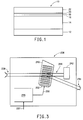
- Figure 1 is a side or edge view of a recently invented photosensitive flexographic printing element, comprising, in order, from bottom to top, a support, a photopolymerizable layer which is substantially insensitive to infrared radiation, one or more optional barrier layer, an infrared radiation sensitive layer, an optional release layer, and a protective cover layer.
- FIG 2 schematic illustration of an apparatus for ablating an image in the infrared radiation sensitive mask layer of the photopolymer flexographic printing element of Figure 1 in accordance with the present invention.
- Figure 3 is a schematic illustration of an acousto-optic modulator assembly for modulating a laser output beam with image data.
- Figure 4 is a cross sectional view of a first arrangement of the element on a first rotatable drum generally along line 4-4 in Figure 2 in the direction of the arrows.
- Figure 5 is a cross sectional view of a second arrangement of the element on a sleeve which in turn is on a second rotatable drum generally along line 4-4 in Figure 2 in the direction of the arrows.
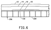
- Figure 6 is a cross sectional view of a third arrangement of the element on the second rotatable drum generally along line 6-6 in Figure 5 in the direction of the arrows.
- an apparatus 200 for exposing an image in at least one infrared radiation sensitive layer 18 of a photosensitive material or element 10 in accordance with the present invention is provided.
- the layer 18 can be any infrared sensitive layer,where exposure to infrared radiation causes a physical or chemical change to material in the layer 18. Such changes include melting, hardening, softening, removing, color density changes, etc.
- the photosensitive element 10 preferably comprises a flexographic printing element or material 10 comprising, in order, a support or cushion layer 12, at least a photopolymerizable layer 14 which is substantially insensitive to infrared radiation, one or more optional barrier layer 16, and the at least one infrared radiation sensitive layer 18.
- a flexographic printing element or material 10 comprising, in order, a support or cushion layer 12, at least a photopolymerizable layer 14 which is substantially insensitive to infrared radiation, one or more optional barrier layer 16, and the at least one infrared radiation sensitive layer 18.
- the layer can be made of a plurality of layers of the same or varying thickness where the layers comprise the same or different composition.
- the layer 18 is ablatable by radiation having a peak power density of 0.1 megaWatts/cm 2 to 17 megaWatts/cm 2 and an energy density of 0.5 Joules/cm 2 to 5 Joules/cm 2 without ablating or polymerizing the photopolymerizable layer 14.
- the layer 18 is ablatable by radiation having a peak power density of 0.5 megaWatts/cm 2 to 9 megaWatts/cm 2 and an energy density of 1 Joules/cm 2 to 3 Joules/cm 2 without ablating or polymerizing the photopolymerizable layers 14.
- the layer 18 is ablatable by radiation having a peak power density of 2 megaWatts/cm 2 to 7 megaWatts/cm 2 and an energy density of 1.4 Joules/cm 2 to 2.7 Joules/cm 2 without ablating or polymerizing the photopolymerizable layer 14.
- the photosensitive element 10 can also include a temporary coversheet 22 on top of the infrared-sensitive layer 18.
- the purpose of the coversheet 22 is to protect the infrared-sensitive layer 18 during storage and handling. It is important that the coversheet 22 be removed prior to exposing the infrared-sensitive layer 18 to infrared laser radiation.
- An optional release layer 20 can be interposed between the coversheet 22 and the infrared-sensitive layer 18 to facilitate removal of the coversheet 22 from the infrared radiation sensitive layer 18.
- the optional release layer 20 is preferably removed with the coversheet 22.
- the photopolymerizable layer 14 comprise an elastomeric binder, at least a monomer and at least an initiator having sensitivity to non-infrared actinic radiation.
- the photopolymerizable layer 14 is soluble, swellable or dispersible in a developer solution.
- the barrier layer 16 is substantially transparent to non-infrared actinic radiation.
- the barrier layer 16 is soluble, swellable, dispersible, or liftable in the developer solution for the photopolymerizable layer 14.
- the infrared radiation sensitive layer 18 is substantially opaque to non-infrared actinic radiation. Suitable preferred photosensitive printing elements 10 are disclosed in U.S. patent 5,262,275, U.S. patent application serial numbers 08/130,610 and 08/341,731, and U.S. patent applications IM-1002 and IM-0971, which are hereby incorporated by reference.
- the thickness of the infrared-sensitive layer 18 should be in a range to optimize both sensitivity and opacity.
- the layer 18 should be thin enough to provide good sensitivity, i.e., the infrared-sensitive layer 18 should be removed rapidly upon exposure to infrared laser radiation.
- the layer 18 should be thick enough so that areas of the layer 18 which remain on the photopolymerizable layer 14 after imagewise exposure effectively mask the photopolymerizable layer 14 from non-infrared actinic radiation.
- the infrared-sensitive layer 18 will have a thickness from about 20 Angstroms to about 50 micrometers. It is preferred that the thickness be from 40 Angstroms to 40 micrometers.
- the apparatus 200 comprises an element support assembly 210, a laser assembly 212, an optical assembly 214, a modulated beam delivery carriage assembly 216, a computer assembly 218, and an electronic control assembly 220.
- the element support assembly 210 includes a rotatable cylindrical surface 222 and an element rotator motor assembly 224.
- the element support assembly 210 further comprises a stationary support frame 226 and a rotatable element support mechanism 228 supporting the cylindrical surface 222 which is rotatably supported at end portions by the support frame 226.
- the mechanism 228 can be a drum or shaft where an outer surface of the drum or shaft is the cylindrical surface 222.
- the mechanism 228 can be a mandrel or cylindrical axle 228 for inserting through a support sleeve 126 which comprises the cylindrical surface 222.
- the support sleeve 126 can be any material including a polymer, such as polyester, or a metal, such as nickel or a nickel alloy. See Figure 5.
- the cylindrical surface 222 is an outer surface of the support sleeve 126
- one end of the support frame 226 can be moved with respect to the drum 228 so the support sleeve 226 can be slid onto the drum 228.
- the mechanism 228 is a set of support end cape or hubs for inserting in and holding ends of the support sleeve 126 in which case the support sleeve 126 again comprises the cylindrical surface 222.
- the cylindrical surface 222 has a longitudinal axis which is coincident with a longitudinal axis of the mechanism 228 (and the sleeve 126 when mounted on the mechanism 228). In each case, the cylindrical surface 222 has a preferred circumference of 24 inches to 50 inches.
- the photopolymer printing material 10 is adapted to be mounted on the cylindrical surface 222 with the infrared radiation sensitive layer 18 facing radially away from the cylindrical surface 222.
- the photopolymer printing material 10 is adapted to be mounted on the cylindrical surface 222 with the infrared radiation sensitive layer 18 facing radially towards the cylindrical surface 222.
- the element rotator motor assembly 224 is for rotating the cylindrical surface 222 and thereby the element 10 mounted on the cylindrical surface 222.
- the temporary coversheet 22 and the release layer 20, if present, should be removed prior to mounting the element 10 on the mechanism 228 and thus prior to imagewise ablation of the infrared sensitive layer 18.
- the element rotator motor assembly 224 is capable of rotating the cylindrical surface 222 at a speed of about 500 to about 2500 revolutions per minute.
- the element rotator motor assembly 224 rotates the cylindrical surface 222 at a speed of about 700 to about 2500 revolutions per minute, and most preferably at a speed of about 1000 to about 2000 revolutions per minute.
- Surface velocity of a point on the cylindrical surface 222 is about 5 meters/second to about 53 meters/second.
- the laser assembly 212 is for producing an image modulated beam 230.
- the laser assembly 212 comprises a laser 232, a laser power supply 234 and an acousto-optic modulator assembly 236.
- the laser 232 is for emitting an output infrared radiation beam 238 having a M 2 beam quality value or factor of 4 to 8 and a maximum power of about 50 Watts to 70 Watts.
- the beam 238 has a M 2 beam quality value of 5 to 7 and, most preferably, a M 2 beam quality value of 5.5 to 6.5.
- the M 2 beam quality value of lasers see A. E. Siegman, New Developments in Laser Resonators, SPIE Vol.
- the laser output beam 238 has a 1/e 2 irradiance diameter at its waist diameter of 2 millimeters to 3 millimeters.
- Diode lasers emitting in the region of 750 to 880 nm offer substantial advantages in terms of their small size, low cost, stability, reliability, ruggedness and ease of modulation.
- Diode lasers emitting in the range of 780 to 850 nm are preferred.
- Such lasers are commercially available from, for example, Spectra Diode Laboratories (San Jose, CA).
- the laser 232 is a Nd:YAG laser which is adapted to emit at about 1064 nm.
- the laser power supply 234 is for energizing the laser 232 over line 233.
- the acousto-optic modulator assembly 236 is for modulating the laser output beam 238 with image data and for producing the image modulated beam 230 which can be a first order beam having a maximum power of about 22 Watts to about 32 Watts.
- the image modulated beam 230 has a wavelength of about 780 nanometers to about 2000 nanometers.
- the acousto-optic modulator assembly 236 is adapted to provide an image modulation rate in a range of about 0.5 megabits/second to about 1.0 megabits/second.
- the acousto-optic modulator assembly 236 comprises an acousto-optic modulator 240 and a beam dump 242.
- the acousto-optic modulator 240 is for diffracting a first order beam portion (which in Figure 3 is beam 230) of the laser output beam 238 and passing a zero order beam portion 244 of the laser output beam 238.
- the beam dump 242 is for blocking either the first order beam portion 230 of the laser output beam 238 or the zero order beam portion 244 of the laser output beam 238.
- the acousto-optic modulator assembly 236 further comprises a radio frequency (RF) driver 246 which receives image data over a line 237 from the electronic control assembly 220.
- RF radio frequency
- the RF driver 246 sends an RF drive signal over a line 250 to a transducer 252 of the acousto-optic modulator 240.
- a suitable acousto-optic modulator 240 is commercially available under model number AOM-40R from IntraAction Corporation of Bellwood, Illinois.
- a suitable RF driver 246 is commercially available under model ME (Signal Processor) also from IntraAction Corporation.
- the optical assembly 216 includes a lens 262 mounted on a lens support 264, a linear track 266, and a focusing motor assembly 268.
- a reflector 260 is included in the optical assembly 216.
- the reflector 260 is for directing the image modulated beam 230 onto the infrared sensitive layer 18 of the material 10 on the cylindrical surface 222.
- the lens 262 is for focusing the directed beam at the infrared sensitive layer 18 of the material 10 on the cylindrical surface 222.
- the modulated beam focused by the lens 262 comprises infrared radiation having a peak power density of 0.1 megaWatts/cm 2 to 17 megaWatts/cm 2 and provides an energy density of 0.5 Joules/cm 2 to 5 Joules/cm 2 on the layer 18.
- the focused modulated beam has a peak power density of 0.5 megaWatts/cm 2 to 9 megaWatts/cm 2 arid provides an energy density of 1 Joules/cm 2 to 3 Joules/cm 2 .
- the focused modulated beam has a peak power density of 2 megaWatts/cm 2 to 7 megawatts/cm 2 and provides an energy density of 1.4 Joules/cm 2 to 2.7 Joules/cm 2 .
- the lens 262 is adapted to focus the directed beam to have a 1/e 2 irradiance diameter of 15 ⁇ m to 30 ⁇ m at the infrared sensitive layer 18 of the material 10 on the cylindrical surface 222.
- the lens 262 focuses the beam to a 1/e 2 irradiance diameter of 20 ⁇ m to 25 ⁇ m at the infrared sensitive layer 18.
- the focusing motor assembly 268 is for moving the lens 262 with respect to the infrared sensitive layer 18 of the material 10 on the cylindrical surface 222 to focus the modulated beam such that the focused modulated beam is adapted to ablate the infrared sensitive layer 18.
- the linear track 266 can be a worm gear connected at one end to a drive shaft of the focusing motor assembly 268.
- the worm gear 266 can be adapted to engage a mating socket in the lens support 264 such that when the focusing motor assembly 268 rotates the word gear 266, the lens support 264 and the lens 262 move linearly along the track 266.
- the optical assembly 216 can be mounted on a carriage 280 which can block rotational movement of the lens support 264 during its linear movement along the track 266.
- the laser assembly 212 can be mounted on the carriage 280 in which case the reflector 260 is unnecessary.
- One or more additional reflector 261 can be used to direct the beam 230 onto the reflector 260 or lens 262 in order to position the laser 232 in a compact position in the apparatus 200.
- a beam expander 263 can be use to increase the diameter of the modulated beam 230.
- Peak Power Density 8 P T ⁇ d o 2
- the term "ablated” means removed by cutting, erosion, melting, evaporation, burning, decomposition, vaporization or the like.
- the term “engrave” is defined as to impress deeply to cut figures, letters, or images into a substrate to form a relief surface to be inked in the printing process.
- the term "engrave” is defined to be synonymous with the word “ablate” with the understanding that the depth of material removed is much less than prior engraving processes, the material being removed is different than in prior engraving processes, and the resulting engraved layer is used as a photomask for forming a printing relief surface from another layer removed from the engraved layer, rather than used as the printing relief surface itself.
- the modulated beam delivery carriage assembly 216 includes the carriage 280, a linear track 282 and a translator motor assembly 284.
- the carriage 280 as stated before supports the optical assembly 214.
- the carriage 280 is adapted to move linearly along the track 282, for instance, in a manner similar to the way the lens support 264 moves along the track 266.
- the track 282 is parallel to the longitudinal axis of the cylindrical surface 222.
- the translator motor assembly 284 is for transporting the carriage 280 along the track 282 to scan the image modulated beam along the infrared sensitive layer 18 of the material 10 on the cylindrical surface 222 at a carriage advance rate of about an ablating width of the modulated beam on the infrared sensitive layer 18 of the material 10 on the cylindrical surface 222.
- the computer assembly 218 is for (i) receiving, generating and/or storing the image data representing an image to be ablated in the infrared radiation sensitive layer 18, and (ii) selecting exposure parameters from a set consisting of the speed of the cylindrical surface 222, the advance rate of the carriage 280, image placement coordinates on the infrared radiation sensitive layer 18, focus position of the lens 262, and amplitude modulation level provided by the acousto-optic modulator assembly 236.
- the electronic control assembly 220 is for receiving the image data and the exposure parameters from the computer assembly 218 over line 219 and processing the image data and the exposure parameters to control the support assembly 210 over line 211 to the motor assembly 224, the laser assembly 212 over lines 213 and 237, the optical assembly 214 over line 215 to the motor assembly 268, and over line 217 to the motor assembly 284 of the modulated beam delivery carriage assembly 216 to ablate the image in a spiral fashion in the infrared radiation sensitive layer 18 without ablating or polymerizing the photopolymerizable layer 14 beneath the infrared sensitive layer 18. See Figure 4.
- An encoder 270 which is connected to the motor assembly 224 provides feedback on the operation of the motor assembly 224 to the electronic control assembly 220 over line 272.
- the electronic control assembly 220 is also adapted to control the acousto-optic modulator assembly 236 over line 237.
- the electronic control assembly 220 is further adapted to be used to select at least one exposure parameter from a set consisting of the cylindrical surface speed, the carriage advance rate, the image placement coordinates on the infrared radiation sensitive layer 18, the lens focus position and the amplitude modulation level.
- the ablating apparatus 200 preferably further comprises a debris extraction system 286 for removing ablated material. Then the electronic control assembly 220 would be adapted to control the debris extraction system 286 over line 287.
- the debris extraction system 286 can be mounted on, and thereby move with, the carriage 280.
- the debris extraction system 286 can be the same as or similar to the debris extraction system in any of the commercially available Grapholas® systems.
- the ablating apparatus 200 preferably further comprises means for mounting the material 10 on the cylindrical surface 222.
- the mounting means can be any means such as a sheet 127 of tape with adhesive layers on both sides as shown in Figure 4.
- the tape is preferably placed on the drum 228 and then the support layer 12 is mounted on the tape 127.
- the mounting means can comprise clamps or a vacuum retaining system 290 as shown in Figures 2 and 5.
- the vacuum retaining system 290 can comprise a vacuum and/or pressure source 292 connected by a conduit 294 to an interior cavity 295 within the drum 228 having closed ends.
- the conduit 294 can be connected through one of the ends of the drum 228 through a rotatable air tight connection.
- Passages 296 extend radially through the drum 228 from the interior cavity 295 to the cylindrical surface 222.
- the vacuum force secures the element 10 to, and prevents the element 10 from moving with respect to, the drum 228.
- the layer 12 can be mounted in direct contact with the drum 228.
- the element 10 can be secured by a sheet 128 of double sided cushion tape to the sleeve 126 which, in turn, is mounted on the drum 228.
- the cushion tape 128 can be the same as tape 127 or provide more cushion for the element 10.
- Figure 6 illustrates the arrangement where the photopolymer printing material 10 is adapted to be mounted on the cylindrical surface 222 with the infrared radiation sensitive layer 18 facing radially towards the cylindrical surface 222.
- a material capture sheet 130 as described in U.S. Patent Application IM-0971 is placed on the cylindrical surface 222 of the vacuum drum 228.
- the element 10 is placed on the material capture sheet 130 and on areas of the cylindrical surface 222 surrounding the material capture sheet.
- a vacuum force from source 292 secures the material capture sheet 130 and the element 10 on the drum 228.
- any means can be used for mounting the material capture sheet 130 and the element 10 on the drum 228.
- the imagewise exposure to infrared radiation and an overall exposure to actinic radiation including non-infrared radiation such as visible and/or ultraviolet radiation can be carried out in the apparatus 200.
- flexographic printing plate or element encompasses plates or elements in any form suitable for flexographic printing, including, but not limited to, flat sheets and seamless continuous cylindrical forms.
- the photopolymerizable flat sheet elements 10 can be reprocessed by wrapping the element 10 around a cylindrical form, such as the printing sleeve 126 or a printing cylinder itself, and fusing the edges together to form a seamless, continuous element.
- Continuous printing elements have applications in the flexographic printing of continuous designs such as in wallpaper, decoration and gift wrapping paper. Furthermore, such continuous printing elements are well-suited for mounting on the laser apparatus 200.
- the sleeve or cylinder on which the printing element 10 is wrapped when the edges are fused, can be mounted directly into the laser apparatus 200 where it functions as the cylindrical surface 222.
- the process of the invention involves (1) providing the photosensitive printing element 10 as described above; (2) imagewise ablating the infrared sensitive layer 18 of the element 10 with an infrared laser radiation beam having a peak power density as defined above and an energy density as defined above from the apparatus 200 to form a mask; (3) overall exposing the photosensitive element to non-infrared actinic radiation through the mask; and (4) treating the product of step (3) with at least one developer solution to remove (i) the infrared-sensitive layer 18 which was not removed during step (2), (ii) at least areas of the barrier layer(s) 16, if present, which were not exposed to non-infrared actinic radiation, and (iii) areas of the photopolymerizable layer 14 which were not exposed to non-infrared actinic radiation.
- the coversheet 22 and the optional release layer 20, if present, is/are removed from the element 10.
- the element 10 is mounted on the rotatable cylindrical surface 222 of the support assembly 228.
- the imagewise ablating step is performed by directing the focused modulated beam on the photosensitive element 10.
- material in the infrared-sensitive layer 18 is removed, i.e., ablated or engraved, in the areas exposed to the infrared laser radiation.
- the areas exposed to laser radiation in the infrared-sensitive layer 18 correspond to those areas in the photopolymerizable layer 14 which will be polymerized to form the final printing plate.
- a pattern of actinic radiation-opaque material remains on the barrier layer 16 or directly on the photopolymerizable layer 14 when the barrier layer 16 is not present.
- the areas in which the infrared-sensitive layer 18 remains correspond to the areas of the photopolymerizable layer 14 which will be washed out in the formation of the final printing plate.
- the ablating step is performed by rotating the cylindrical surface 222 at a speed as described above whale simultaneously moving the optical assembly 214 generally parallel to a longitudinal axis of the cylindrical surface 222 to ablate an image in a spiral fashion in the infrared sensitive layer 18 at an advance rate of about an ablating width on the layer 18 per revolution of the cylindrical surface 222. This is done with the infrared laser radiation beam focused to have a diameter as described above.
- the next step in the process of the invention is to overall expose the photosensitive element 10 to actinic radiation through the mask.
- the type of radiation used is dependent on the type of photoinitiator in the photopolymerizable layer 18.
- the radiation-opaque material in the infrared sensitive layer 18 which remains on top of the barrier layer 16 on the photopolymerizable layer 14 prevents the material beneath from being exposed to the radiation and hence those areas covered by the radiation-opaque material do not polymerize.
- the areas not covered by the radiation-opaque material are exposed to actinic radiation and polymerize. Any conventional sources of actinic radiation can be used for this exposure step.
- Suitable visible or UV sources include carbon arcs, mercury-vapor arcs, fluorescent lamps, electron flash units, electron beam units and photographic flood lamps.
- the most suitable sources of UV radiation are the mercury-vapor lamps, particularly the sun lamps.
- a standard radiation source is the Sylvania 350 Blacklight fluorescent lamp (FR 48T12/350 VL/VHO/180, 115 w) which has a central wavelength of emission around 354 nm.
- the actinic radiation exposure time can vary from a few seconds to minutes, depending upon the intensity and spectral energy distribution of the radiation, its distance from the photosensitive element 10, and the nature and amount of the photopolymerizable composition in layer 14.
- a mercury vapor arc or a sunlamp is used at a distance of about 1.5 to about 60 inches (3.8 to 153 cm) from the photosensitive element 10.
- Exposure temperatures are preferably ambient or slightly higher, i.e., about 20° to about 35°C.
- the process of the invention usually includes a back exposure or backflash step.
- This is a blanket exposure to actinic radiation through the support or cushion layer 12. It is used to create a shallow layer of polymerized material, or a floor, on the support side of the photopolymerizable layer 14 and to sensitize the photopolymerizable layer 14.
- the floor provides improved adhesion between the photopolymerizable layer 14 and the support or cushion layer 12, helps highlight dot resolution and also establishes the depth of the plate relief.
- the backflash exposure can take place before, after or during the other imaging steps (i.e., the ablating step and the exposing step). It is preferred that it take place just prior to the imagewise ablating with infrared laser radiation on the infrared-sensitive layer 18 side of the element 10.
- Exposure time generally range from a few seconds up to about a minute.
- the image is treated or developed by washing with a suitable developer.
- the developer removes (i) the infrared-sensitive material which was not removed during the ablation step, (ii) the barrier layer 16, if present, in at least the areas which were not exposed to non-infrared actinic radiation, and (iii) the photopolymerizable layer 14 in the areas which were not exposed to non-infrared actinic radiation. Development is usually carried out at about room temperature.
- the developers can be organic solutions, water, aqueous or semi-aqueous solutions. The choice of the developer will depend on the chemical nature of the photopolymerizable material to be removed.
- Suitable organic solution developers include aromatic or aliphatic hydrocarbon and aliphatic or aromatic halohydrocarbon solutions, or mixtures of such solutions with suitable alcohols.
- Other organic solution developers have been disclosed in published German Application 38 28 551 and U.S. Patent 5,354,645.
- Suitable semi-aqueous developers usually contain water and a water miscible organic solution and an alkaline material.
- Suitable aqueous developers usually contain water and an alkaline material.
- Other suitable aqueous developer combinations are described in U.S. Patent 3,796,602.
- Development time can vary, but it is preferably in the range of about 2 to 25 minutes.
- Developer can be applied in any convenient manner, including,immersion, spraying and brush or roller application.
- Brushing aids can be used to remove the unpolymerized portions of the composition.
- washout is frequently carried out in an automatic processing unit which uses developer and mechanical brushing action to removed the unexposed portions of the plate, leaving a relief constituting the exposed image and the floor.
- a pre-development step may be necessary if the infrared-sensitive layer 18 is not removable by the developer solution.
- An additional developer which does not effect the polymerized photosensitive material can be applied to remove the infrared-sensitive layer first. This is particularly true when metallic materials are used. In such cases, etching solutions are used, such as 2% aqueous KOH solution.
- the process of this invention may be simplified by removing in the treating step with brushing the infrared sensitive layer 18, and/or the barrier layer 16, if present, at the same time as the removal of the unexposed portions of the photopolymer layer 14.
- the pretreating step may not be necessary in the situation in which the photosensitive element 10 includes a infrared sensitive layer 18 and/or barrier layer 16 which is not substantially soluble, swellable, dispersible, or liftable in the developer solution for the photopolymer layer 14.
- the infrared sensitive layer 18 and the barrier layer 16 are generally much thinner than the photopolymer layer 14 such that with the aid of brushing or brushing with pressure, the infrared and barrier layers 18,16 can be easily removed from the photopolymer layer 14. Since automatic processing units which use mechanical brushing action are in use commercially for development of photopolymeric plates, the need for brushing action during washout is easily accomplished.
- the relief printing plates are generally blotted or wiped dry, and then dried in a forced air or infrared oven. Drying times and temperatures may vary, however, typically the plate is dried for 60 to 120 minutes at 60°C. High temperatures are not recommended because the support 12 can shrink and this can cause registration problems.
- This post-exposure step utilizes the same radiation source as the main exposure to actinic radiation including non-infrared radiation.
- Detackification is an optional post-development treatment which can be applied if the surface is still tacky, such tackiness not generally being removed in post-exposure. Tackiness can be eliminated by methods well known in the art, such as treatment with bromine or chlorine solutions. Such treatments have been disclosed in, for example, Grüetzmacher U.S. Patent 4,400,459, Fickes et al., U.S. Patent 4,400,460 and German Patent 28 23 300. Detackification can also be accomplished by exposure to radiation sources having a wavelength not longer than 300 nm, as disclosed in European Published Patent Application 0 017 927 and Gibson U.S. Patent 4,806,506.
- Imagewise ablation, overall exposure, development and any additional steps can be performed while the plate is mounted in the round.
- Other advantages which can be obtained using the instant process include increased process speed, better registration and reduced or in some cases no extra mounting time.
Abstract
Description
- This invention relates to an apparatus and process for imagewise exposing an infrared sensitive layer and, more specifically, for imagewise ablating an infrared radiation sensitive layer of a flexographic printing element for use in making a flexographic printing plate.
- Flexographic printing plates are well known for use in letterpress printing, particularly on surfaces which are soft and easily deformable, such as packaging materials, e.g., cardboard, plastic films, etc. Flexographic printing plates can be prepared from photopolymerizable compositions, such as those described in U.S. patents 4,323,637 and 4,427,749. The photopolymerizable compositions generally comprise an elastomeric binder, at least one monomer and a photoinitiator. Photosensitive elements generally have a photopolymerizable layer interposed between a support and a coversheet or multilayer cover element. Upon imagewise exposure to actinic radiation, polymerization, and hence, insolubilization of the photopolymerizable layer occurs in the exposed areas. Treatment with a suitable solution removes the unexposed areas of the photopolymerizable layer leaving a printing relief which can be used for flexographic printing.
- Imagewise exposure of a photosensitive element requires the use of a phototool which is a mask having clear and opaque areas covering the photopolymerizable layer. The phototool prevents exposure and polymerization in the opaque areas. The phototool allows exposure to radiation in the clear areas so that these areas polymerize and remain on the support after the development step. The phototool is usually a photographic negative of the desired printing image. If corrections are needed in the final image a new negative must be made. This is a time-consuming process. In addition, the phototool may change slightly in dimension due to changes in temperature and humidity. Thus, the same phototool, when used at different times or in different environments, may give different results and could cause registration problems.
- Thus, it would be desirable to eliminate the phototool by directly recording information on a photosensitive element, e.g., by means of a laser beam. The image to be developed could be translated into digital information and the digital information used to place the laser for imaging. The digital information could even be transmitted from a distant location. Corrections could be made easily and quickly by adjusting the digitized image. In addition, the digitized image could be either positive or negative, eliminating the need to have both positive-working and negative-working photosensitive materials, or positive and negative phototools. This saves storage space and, thus, reduces cost. Another advantage is that registration can be precisely controlled by machine during the imaging step. Digitized imaging without a phototool is particularly well-suited for making seamless, continuous printing forms.
- In general, it has not been very practical to use lasers to image the elements which are used to prepare flexographic printing plates. The elements have low photosensitivity and require long exposure times even with high powered lasers. In addition, most of the photopolymerizable materials used in these elements have their greatest sensitivity in the ultraviolet range. While UV lasers are known, economical and reliable UV lasers with high power are generally not available. However, non-UV lasers are available which are relatively inexpensive, and which have a useful power output and which can be utilized to form a mask image on top of flexographic printing elements.
- In view of these facts, a
photosensitive printing element 10 has recently been developed for use in preparing flexographic print plates. Referring from bottom to top in Figure 1, the photosensitive printing element comprises, in order, a support orcushion layer 12, at least onephotopolymerizable layer 14 which is substantially insensitive to infrared radiation, one or moreoptional barrier layer 16, and at least an infrared radiationsensitive layer 18. A removableprotective coversheet 22 with anoptional release layer 20 cover and protect the outer infrared radiationsensitive layer 18. See, for instance, U.S. patent 5,262,275 and U.S. patent application serial numbers 08/130,610 and 08/341,731. Also see U.S. patent applications IM-1002 and IM-0971, assigned to E. I. du Pont de Nemours and Company and filed on the same day as this application. The process of using these photosensitive printing elements involves (1) removing anyprotective coversheet 22 and therelease layer 20, if present; (2) imagewise ablating the infrared-sensitive layer 18 to form a mask; (3) overall exposing thephotosensitive element 10 to non-infrared actinic radiation through the mask; and (4) treating the product of step (3) with at least one developer solution to remove (i) the infrared-sensitive material which was not removed during step (2), (ii) at least the areas of anybarrier layer 16, if present, which were not exposed to non-infrared actinic radiation, and (iii) the areas of thephotopolymerizable layer 14 which were not exposed to non-infrared actinic radiation. The treating step (4) produces a flexographic printing plate with a relief surface or image which is inked and used for flexographic printing of typically multiple copies of the inked portions of the relief surface or image. - Conventional laser engraving systems are available for directly engraving relief images in materials for directly producing relief printing surfaces. Typical laser engravers use CO2 lasers which emit a highly multi-mode beam having a wavelength of about 10.6 microns which are very powerful lasers that would burn through or vaporize most polymers including polymers in conventional flexographic printing elements and the entire elements disclosed in U.S. patent 5,262,275, U.S. patent application serial numbers 08/130,610 and 08/341,731, and U.S. patent applications IM-1002 and IM-0971. Such engravers typically have a minimum resolution or beam diameter of about 40 microns which is much too large for creating a high resolution flexographic printing mask. The maximum modulation rate of a CO2 laser is about 20 kHz which causes the maximum engraving speed to be too slow for a commercially viable system for forming high resolution mask layers on flexographic printing elements.
- The Grapholas® system made and sold by Baasel-Scheel Lasergraphics, Gmbh, of Itzehoe, Germany, is for directly engraving relief images in a layer for directly producing relief printing surfaces. The Grapholas® system comprises:
- a support assembly including:
- a support,
- a drum rotatably mounted on the support, the drum having an outer cylindrical surface, the layer adapted to be mounted on the cylindrical surface, and
- a drum motor assembly mounted on the support, the drum motor assembly for rotating the drum with a maximum speed of about 200 rpm;
- a CO2 laser assembly for producing an image modulated beam;
- an optical assembly including:
- a lens for focusing the directed beam having a minimum resolution of about 40 microns at the layer on the cylindrical surface, and
- a focusing motor assembly for moving the lens with respect to the layer on the cylindrical surface to focus the modulated beam such that the focused modulated beam is adapted to engrave the layer;
- a modulated beam delivery carriage assembly including:
- a carriage for supporting the optical assembly,
- a linear track along which the carriage is adapted to move, the track parallel to the longitudinal axis, and
- a translator motor assembly for transporting the carriage along the track to scan the image modulated beam along the layer on the cylindrical surface at a carriage advance rate of about an engraving width of the modulated beam on the layer on the cylindrical surface;
- a computer assembly for (i) receiving, generating and/or storing the image data representing an image to be engraved in the layer, and (ii) selecting exposure parameters from a set consisting of the cylindrical surface speed, the support advance rate, image placement coordinates on the layer, focusing position, and amplitude modulation level; and
- an electronic control assembly for receiving the image data and the exposure parameters from the computer assembly and processing the image data and the exposure parameters to control the support assembly, the laser assembly, the optical assembly, and the linear transport mechanism to engrave the image in a spiral fashion in the layer.
- Another engraving system previously made and sold by Baasel Lasertechnik, Gmbh called the Grapholas® Compact system was also for directly engraving relief images in a layer for directly producing relief printing surfaces. The Grapholas® Compact system comprised:
- a support assembly including:
- a support,
- a drum rotatably mounted on the support, the drum having an outer cylindrical surface, the layer adapted to be mounted on the cylindrical surface, and
- a drum motor assembly mounted on the support, the drum motor assembly for rotating the drum with a maximum speed of about 106 rpm;
- a laser assembly for producing an image modulated beam, the laser assembly comprising:
- a Nd:YAG laser for emitting an output infrared radiation beam,
- a laser power supply for energizing the laser, and
- a Q-switch for image modulating the output infrared radiation beam;
- a stationary (i.e., fixed) optical assembly including:
- a lens for focusing the directed beam at the layer on the cylindrical surface, and
- a focusing motor assembly for moving the lens with respect to the layer on the cylindrical surface to focus the modulated beam such that the focused modulated beam is adapted to engrave the layer;
- a linear transport mechanism for transporting the support, the drum and the drum motor assembly along a line to scan the image modulated beam along the layer on the cylindrical surface at a carriage advance rate of about an engraving width of the modulated beam on the layer on the cylindrical surface;
- a computer assembly for (i) receiving, generating and/or storing the image data representing an image to be engraved in the layer, and (ii) selecting exposure parameters from a set consisting of the cylindrical surface speed, the support advance rate, image placement coordinates on the layer, focusing position, and amplitude modulation level; and
- an electronic control assembly for receiving the image data and the exposure parameters from the computer assembly and processing the image data and the exposure parameters to control the support assembly, the laser assembly, the optical assembly, and the linear transport mechanism to engrave the image in a spiral fashion in the layer.
- Since the structure and properties of the photosensitive printing elements disclosed in U.S. patent 5,262,275, U.S. patent application serial numbers 08/130,610 and 08/341,731, and U.S. patent applications IM-1002 and IM-0971 are different than other materials that have been engraved by conventional engraving machines, such machines are not capable of forming a mask from the infrared radiation sensitive layer of the photosensitive printing elements disclosed in U.S. patent 5,262,275, U.S. patent application serial numbers 08/130,610 and 08/341,731, and U.S. patent applications IM-1002 and IM-0971 in a commercially viable manner.
- In fact, since these unique photosensitive printing elements were only recently developed, no apparatus is commercially available which is capable of ablating the infrared radiation sensitive layer of these photosensitive printing elements to form a suitable mask for use in preparing flexographic printing plates with desired productivity and image quality.
- The invention provides an apparatus for imagewise exposing an infrared sensitive layer, the apparatus comprising:
- a support assembly including:
- a rotatable cylindrical surface having a longitudinal axis, the layer adapted to be mounted on the cylindrical surface, and
- a motor assembly for rotating the cylindrical surface;
- a laser assembly for producing an image modulated beam;
- an optical assembly including:
- a lens for focusing the directed beam at the layer on the cylindrical surface, and
- a focusing motor assembly for moving the lens with respect to the layer on the cylindrical surface to focus the modulated beam such that the focused modulated beam is adapted to engrave the layer;
- a modulated beam delivery carriage assembly including:
- a carriage for supporting the optical assembly,
- a linear track along which the carriage is adapted to move, the track parallel to the longitudinal axis, and
- a translator motor assembly for transporting the carriage along the track to scan the image modulated beam along the layer on the cylindrical surface at a carriage advance rate of about an exposing width of the modulated beam on the layer on the cylindrical surface;
- a computer assembly for (i) receiving, generating and/or storing image data representing an image to be exposed on the layer, and (ii) selecting exposure parameters from a set consisting of the cylindrical surface speed, the carriage advance rate, image placement coordinates on the layer, focusing position, and amplitude modulation level; and
- an electronic control assembly for receiving the image data and the exposure parameters from the computer assembly and processing the image data and the exposure parameters to control the support assembly, the laser assembly, the optical assembly, and the modulated beam delivery carriage assembly to expose the image in a spiral fashion in the layer; and wherein the improvement comprises:
- the focused modulated beam comprises infrared radiation having a peak power density of 0.1 megaWatts/cm2 to 17 megaWatts/cm2 and is adapted to provide an energy density of 0.5 Joules/cm2 to 5 Joules/cm2 on the layer.
- The invention is further directed to a process for making a flexographic printing plate, comprising:
- (1) providing a photosensitive printing element comprising in the order listed:
- (a) a support layer,
- (b) at least a photopolymerizable layer comprising an elastomeric binder, at least a monomer and at least an initiator having sensitivity to non-infrared actinic radiation, said photopolymerizable layer being soluble, swellable or dispersible in a developer solution;
- (c) optionally at least a barrier layer which is substantially transparent to non-infrared actinic radiation; and
- (d) at least a layer of infrared radiation sensitive material which is substantially opaque to non-infrared actinic radiation;
- (2) imagewise ablating layer (d) with an infrared laser radiation beam having a peak power density of 0.1 megawatts/cm2 to 17 megaWatts/cm2 and adapted to provide an energy density of 0.5 Joules/cm2 to 5 Joules/cm2 from a laser ablating apparatus to form a mask, the apparatus comprising a support assembly, a laser assembly, an optical assembly, a modulated beam delivery carriage assembly, a computer assembly, and an electronic control assembly;
- (3) overall exposing the photosensitive element to non-infrared radiation actinic radiation through the mask; and
- (4) treating the product of step (3) with at least one developer solution to remove (i) the infrared-sensitive layer which was not removed during step (2), (ii) at least areas of the barrier layer, if present, which were not exposed to non-infrared actinic radiation, and (iii) areas of the photopolymerizable layer (b) which were not exposed to non-infrared actinic radiation.
- The invention can be more fully understood from the following detailed description thereof in connection with accompanying drawings described as follows.
- Figure 1 is a side or edge view of a recently invented photosensitive flexographic printing element, comprising, in order, from bottom to top, a support, a photopolymerizable layer which is substantially insensitive to infrared radiation, one or more optional barrier layer, an infrared radiation sensitive layer, an optional release layer, and a protective cover layer.
- Figure 2 schematic illustration of an apparatus for ablating an image in the infrared radiation sensitive mask layer of the photopolymer flexographic printing element of Figure 1 in accordance with the present invention.
- Figure 3 is a schematic illustration of an acousto-optic modulator assembly for modulating a laser output beam with image data.
- Figure 4 is a cross sectional view of a first arrangement of the element on a first rotatable drum generally along line 4-4 in Figure 2 in the direction of the arrows.
- Figure 5 is a cross sectional view of a second arrangement of the element on a sleeve which in turn is on a second rotatable drum generally along line 4-4 in Figure 2 in the direction of the arrows.
- Figure 6 is a cross sectional view of a third arrangement of the element on the second rotatable drum generally along line 6-6 in Figure 5 in the direction of the arrows.
- Throughout the following detailed description, similar reference characters refer to similar elements in all figures of the drawings.
- Referring to Figure 2, there is an
apparatus 200 for exposing an image in at least one infrared radiationsensitive layer 18 of a photosensitive material orelement 10 in accordance with the present invention. Thelayer 18 can be any infrared sensitive layer,where exposure to infrared radiation causes a physical or chemical change to material in thelayer 18. Such changes include melting, hardening, softening, removing, color density changes, etc. - As shown in Figure 1, the
photosensitive element 10 preferably comprises a flexographic printing element ormaterial 10 comprising, in order, a support orcushion layer 12, at least aphotopolymerizable layer 14 which is substantially insensitive to infrared radiation, one or moreoptional barrier layer 16, and the at least one infrared radiationsensitive layer 18. Hereafter, when a single layer is mentioned, it is to be understood that the layer can be made of a plurality of layers of the same or varying thickness where the layers comprise the same or different composition. Thelayer 18 is ablatable by radiation having a peak power density of 0.1 megaWatts/cm2 to 17 megaWatts/cm2 and an energy density of 0.5 Joules/cm2 to 5 Joules/cm2 without ablating or polymerizing thephotopolymerizable layer 14. Preferably, thelayer 18 is ablatable by radiation having a peak power density of 0.5 megaWatts/cm2 to 9 megaWatts/cm2 and an energy density of 1 Joules/cm2 to 3 Joules/cm2 without ablating or polymerizing the photopolymerizable layers 14. Most preferably, thelayer 18 is ablatable by radiation having a peak power density of 2 megaWatts/cm2 to 7 megaWatts/cm2 and an energy density of 1.4 Joules/cm2 to 2.7 Joules/cm2 without ablating or polymerizing thephotopolymerizable layer 14. - The
photosensitive element 10 can also include atemporary coversheet 22 on top of the infrared-sensitive layer 18. The purpose of thecoversheet 22 is to protect the infrared-sensitive layer 18 during storage and handling. It is important that thecoversheet 22 be removed prior to exposing the infrared-sensitive layer 18 to infrared laser radiation. Anoptional release layer 20 can be interposed between thecoversheet 22 and the infrared-sensitive layer 18 to facilitate removal of the coversheet 22 from the infrared radiationsensitive layer 18. Theoptional release layer 20 is preferably removed with thecoversheet 22. Thephotopolymerizable layer 14 comprise an elastomeric binder, at least a monomer and at least an initiator having sensitivity to non-infrared actinic radiation. Thephotopolymerizable layer 14 is soluble, swellable or dispersible in a developer solution. Thebarrier layer 16 is substantially transparent to non-infrared actinic radiation. Preferably, thebarrier layer 16 is soluble, swellable, dispersible, or liftable in the developer solution for thephotopolymerizable layer 14. The infrared radiationsensitive layer 18 is substantially opaque to non-infrared actinic radiation. Suitable preferredphotosensitive printing elements 10 are disclosed in U.S. patent 5,262,275, U.S. patent application serial numbers 08/130,610 and 08/341,731, and U.S. patent applications IM-1002 and IM-0971, which are hereby incorporated by reference. - The thickness of the infrared-
sensitive layer 18 should be in a range to optimize both sensitivity and opacity. Thelayer 18 should be thin enough to provide good sensitivity, i.e., the infrared-sensitive layer 18 should be removed rapidly upon exposure to infrared laser radiation. At the same time, thelayer 18 should be thick enough so that areas of thelayer 18 which remain on thephotopolymerizable layer 14 after imagewise exposure effectively mask thephotopolymerizable layer 14 from non-infrared actinic radiation. In general, the infrared-sensitive layer 18 will have a thickness from about 20 Angstroms to about 50 micrometers. It is preferred that the thickness be from 40 Angstroms to 40 micrometers. - The
apparatus 200 comprises anelement support assembly 210, alaser assembly 212, anoptical assembly 214, a modulated beamdelivery carriage assembly 216, acomputer assembly 218, and anelectronic control assembly 220. - The
element support assembly 210 includes a rotatablecylindrical surface 222 and an elementrotator motor assembly 224. Theelement support assembly 210 further comprises astationary support frame 226 and a rotatableelement support mechanism 228 supporting thecylindrical surface 222 which is rotatably supported at end portions by thesupport frame 226. Themechanism 228 can be a drum or shaft where an outer surface of the drum or shaft is thecylindrical surface 222. Alternatively, themechanism 228 can be a mandrel orcylindrical axle 228 for inserting through asupport sleeve 126 which comprises thecylindrical surface 222. Thesupport sleeve 126 can be any material including a polymer, such as polyester, or a metal, such as nickel or a nickel alloy. See Figure 5. When thecylindrical surface 222 is an outer surface of thesupport sleeve 126, one end of thesupport frame 226 can be moved with respect to thedrum 228 so thesupport sleeve 226 can be slid onto thedrum 228. In another embodiment, themechanism 228 is a set of support end cape or hubs for inserting in and holding ends of thesupport sleeve 126 in which case thesupport sleeve 126 again comprises thecylindrical surface 222. Thecylindrical surface 222 has a longitudinal axis which is coincident with a longitudinal axis of the mechanism 228 (and thesleeve 126 when mounted on the mechanism 228). In each case, thecylindrical surface 222 has a preferred circumference of 24 inches to 50 inches. In a first arrangement illustrated in Figures 4 and 5, thephotopolymer printing material 10 is adapted to be mounted on thecylindrical surface 222 with the infrared radiationsensitive layer 18 facing radially away from thecylindrical surface 222. In a second arrangement illustrated in Figure 6, thephotopolymer printing material 10 is adapted to be mounted on thecylindrical surface 222 with the infrared radiationsensitive layer 18 facing radially towards thecylindrical surface 222. The elementrotator motor assembly 224 is for rotating thecylindrical surface 222 and thereby theelement 10 mounted on thecylindrical surface 222. Referring to Figure 4, thetemporary coversheet 22 and therelease layer 20, if present, should be removed prior to mounting theelement 10 on themechanism 228 and thus prior to imagewise ablation of the infraredsensitive layer 18. Referring back to Figure 2, the elementrotator motor assembly 224 is capable of rotating thecylindrical surface 222 at a speed of about 500 to about 2500 revolutions per minute. Preferably, the elementrotator motor assembly 224 rotates thecylindrical surface 222 at a speed of about 700 to about 2500 revolutions per minute, and most preferably at a speed of about 1000 to about 2000 revolutions per minute. Surface velocity of a point on thecylindrical surface 222 is about 5 meters/second to about 53 meters/second. - The
laser assembly 212 is for producing an image modulatedbeam 230. Thelaser assembly 212 comprises alaser 232, alaser power supply 234 and an acousto-optic modulator assembly 236. Thelaser 232 is for emitting an outputinfrared radiation beam 238 having a M2 beam quality value or factor of 4 to 8 and a maximum power of about 50 Watts to 70 Watts. Preferably, thebeam 238 has a M2 beam quality value of 5 to 7 and, most preferably, a M2 beam quality value of 5.5 to 6.5. For articles defining, and describing methods of measuring, the M2 beam quality value of lasers, see A. E. Siegman, New Developments in Laser Resonators, SPIE Vol. 1224, Optical Resonators (1990); T. F. Johnson, Jr., M2 Concept Characterizes Beam Quality, Laser Focus World, May 1990; and M. W. Sasnett, Characterization of Laser Beam Propagation, Coherent, September 1990. Thelaser output beam 238 has a 1/e2 irradiance diameter at its waist diameter of 2 millimeters to 3 millimeters. - Various infrared lasers can be used. Diode lasers emitting in the region of 750 to 880 nm offer substantial advantages in terms of their small size, low cost, stability, reliability, ruggedness and ease of modulation. Diode lasers emitting in the range of 780 to 850 nm are preferred. Such lasers are commercially available from, for example, Spectra Diode Laboratories (San Jose, CA). Most preferably, the
laser 232 is a Nd:YAG laser which is adapted to emit at about 1064 nm. Thelaser power supply 234 is for energizing thelaser 232 overline 233. The acousto-optic modulator assembly 236 is for modulating thelaser output beam 238 with image data and for producing the image modulatedbeam 230 which can be a first order beam having a maximum power of about 22 Watts to about 32 Watts. The image modulatedbeam 230 has a wavelength of about 780 nanometers to about 2000 nanometers. Preferably, the acousto-optic modulator assembly 236 is adapted to provide an image modulation rate in a range of about 0.5 megabits/second to about 1.0 megabits/second. - Referring to Figure 3, the acousto-
optic modulator assembly 236 comprises an acousto-optic modulator 240 and abeam dump 242. The acousto-optic modulator 240 is for diffracting a first order beam portion (which in Figure 3 is beam 230) of thelaser output beam 238 and passing a zeroorder beam portion 244 of thelaser output beam 238. Thebeam dump 242 is for blocking either the firstorder beam portion 230 of thelaser output beam 238 or the zeroorder beam portion 244 of thelaser output beam 238. The acousto-optic modulator assembly 236 further comprises a radio frequency (RF)driver 246 which receives image data over aline 237 from theelectronic control assembly 220. TheRF driver 246 sends an RF drive signal over aline 250 to atransducer 252 of the acousto-optic modulator 240. A suitable acousto-optic modulator 240 is commercially available under model number AOM-40R from IntraAction Corporation of Bellwood, Illinois. Asuitable RF driver 246 is commercially available under model ME (Signal Processor) also from IntraAction Corporation. - Referring back to Figure 2, the
optical assembly 216 includes alens 262 mounted on alens support 264, alinear track 266, and a focusingmotor assembly 268. Preferably, areflector 260 is included in theoptical assembly 216. Thereflector 260 is for directing the image modulatedbeam 230 onto the infraredsensitive layer 18 of the material 10 on thecylindrical surface 222. Thelens 262 is for focusing the directed beam at the infraredsensitive layer 18 of the material 10 on thecylindrical surface 222. The modulated beam focused by thelens 262 comprises infrared radiation having a peak power density of 0.1 megaWatts/cm2 to 17 megaWatts/cm2 and provides an energy density of 0.5 Joules/cm2 to 5 Joules/cm2 on thelayer 18. Preferably, the focused modulated beam has a peak power density of 0.5 megaWatts/cm2 to 9 megaWatts/cm2 arid provides an energy density of 1 Joules/cm2 to 3 Joules/cm2. Most preferably, the focused modulated beam has a peak power density of 2 megaWatts/cm2 to 7 megawatts/cm2 and provides an energy density of 1.4 Joules/cm2 to 2.7 Joules/cm2. Thelens 262 is adapted to focus the directed beam to have a 1/e2 irradiance diameter of 15 µm to 30 µm at the infraredsensitive layer 18 of the material 10 on thecylindrical surface 222. Preferably, thelens 262 focuses the beam to a 1/e2 irradiance diameter of 20 µm to 25 µm at the infraredsensitive layer 18. The focusingmotor assembly 268 is for moving thelens 262 with respect to the infraredsensitive layer 18 of the material 10 on thecylindrical surface 222 to focus the modulated beam such that the focused modulated beam is adapted to ablate the infraredsensitive layer 18. Thelinear track 266 can be a worm gear connected at one end to a drive shaft of the focusingmotor assembly 268. Theworm gear 266 can be adapted to engage a mating socket in thelens support 264 such that when the focusingmotor assembly 268 rotates theword gear 266, thelens support 264 and thelens 262 move linearly along thetrack 266. Theoptical assembly 216 can be mounted on acarriage 280 which can block rotational movement of thelens support 264 during its linear movement along thetrack 266. Thelaser assembly 212 can be mounted on thecarriage 280 in which case thereflector 260 is unnecessary. One or moreadditional reflector 261 can be used to direct thebeam 230 onto thereflector 260 orlens 262 in order to position thelaser 232 in a compact position in theapparatus 200. If needed, abeam expander 263 can be use to increase the diameter of the modulatedbeam 230. - Assuming a Gaussian laser beam, the peak power density or irradiance occurs at the center of the beam and is given by Formula I below.

- PT
- = Total Power (Watts) in beam; and
- do
- = 1/e2 irradiance diameter of beam.
- PT =
- Total Power (Watts or Joules/sec) in beam;
- rps =
- drum revolutions each second;
- Dc =
- drum circumference (cm); and
- WA =
- advance width (cm) of beam along longitudinal axis of drum each revolution of the drum.
- When the modulated
beam 230 is focused on the infraredsensitive layer 18, material in the infrared-sensitive layer 18 is removed, i.e., ablated or engraved, in the areas exposed to the infrared laser radiation. For the purposes herein, the term "ablated" means removed by cutting, erosion, melting, evaporation, burning, decomposition, vaporization or the like. In the printing field, the term "engrave" is defined as to impress deeply to cut figures, letters, or images into a substrate to form a relief surface to be inked in the printing process. In a preferred use of theapparatus 200 to make flexographic printing plates, the term "engrave" is defined to be synonymous with the word "ablate" with the understanding that the depth of material removed is much less than prior engraving processes, the material being removed is different than in prior engraving processes, and the resulting engraved layer is used as a photomask for forming a printing relief surface from another layer removed from the engraved layer, rather than used as the printing relief surface itself. - The modulated beam
delivery carriage assembly 216 includes thecarriage 280, alinear track 282 and atranslator motor assembly 284. Thecarriage 280 as stated before supports theoptical assembly 214. Thecarriage 280 is adapted to move linearly along thetrack 282, for instance, in a manner similar to the way thelens support 264 moves along thetrack 266. Thetrack 282 is parallel to the longitudinal axis of thecylindrical surface 222. Thetranslator motor assembly 284 is for transporting thecarriage 280 along thetrack 282 to scan the image modulated beam along the infraredsensitive layer 18 of the material 10 on thecylindrical surface 222 at a carriage advance rate of about an ablating width of the modulated beam on the infraredsensitive layer 18 of the material 10 on thecylindrical surface 222. - The
computer assembly 218 is for (i) receiving, generating and/or storing the image data representing an image to be ablated in the infrared radiationsensitive layer 18, and (ii) selecting exposure parameters from a set consisting of the speed of thecylindrical surface 222, the advance rate of thecarriage 280, image placement coordinates on the infrared radiationsensitive layer 18, focus position of thelens 262, and amplitude modulation level provided by the acousto-optic modulator assembly 236. - The
electronic control assembly 220 is for receiving the image data and the exposure parameters from thecomputer assembly 218 overline 219 and processing the image data and the exposure parameters to control thesupport assembly 210 overline 211 to themotor assembly 224, thelaser assembly 212 overlines optical assembly 214 overline 215 to themotor assembly 268, and overline 217 to themotor assembly 284 of the modulated beamdelivery carriage assembly 216 to ablate the image in a spiral fashion in the infrared radiationsensitive layer 18 without ablating or polymerizing thephotopolymerizable layer 14 beneath the infraredsensitive layer 18. See Figure 4. Anencoder 270 which is connected to themotor assembly 224 provides feedback on the operation of themotor assembly 224 to theelectronic control assembly 220 overline 272. Theelectronic control assembly 220 is also adapted to control the acousto-optic modulator assembly 236 overline 237. Theelectronic control assembly 220 is further adapted to be used to select at least one exposure parameter from a set consisting of the cylindrical surface speed, the carriage advance rate, the image placement coordinates on the infrared radiationsensitive layer 18, the lens focus position and the amplitude modulation level. - The
ablating apparatus 200 preferably further comprises adebris extraction system 286 for removing ablated material. Then theelectronic control assembly 220 would be adapted to control thedebris extraction system 286 overline 287. Thedebris extraction system 286 can be mounted on, and thereby move with, thecarriage 280. Thedebris extraction system 286 can be the same as or similar to the debris extraction system in any of the commercially available Grapholas® systems. - The
ablating apparatus 200 preferably further comprises means for mounting thematerial 10 on thecylindrical surface 222. The mounting means can be any means such as asheet 127 of tape with adhesive layers on both sides as shown in Figure 4. In this embodiment, the tape is preferably placed on thedrum 228 and then thesupport layer 12 is mounted on thetape 127. Alternatively, the mounting means can comprise clamps or avacuum retaining system 290 as shown in Figures 2 and 5. Thevacuum retaining system 290 can comprise a vacuum and/orpressure source 292 connected by aconduit 294 to aninterior cavity 295 within thedrum 228 having closed ends. Theconduit 294 can be connected through one of the ends of thedrum 228 through a rotatable air tight connection.Passages 296 extend radially through thedrum 228 from theinterior cavity 295 to thecylindrical surface 222. When thesource 292 creates a vacuum in thecavity 295 and theelement 10 is mounted on thedrum 228, the vacuum force secures theelement 10 to, and prevents theelement 10 from moving with respect to, thedrum 228. In this embodiment, thelayer 12 can be mounted in direct contact with thedrum 228. Alternatively, as shown in Figure 5, theelement 10 can be secured by asheet 128 of double sided cushion tape to thesleeve 126 which, in turn, is mounted on thedrum 228. Thecushion tape 128 can be the same astape 127 or provide more cushion for theelement 10. When thesleeve 126 is used and thesource 292 supplies air to thecavity 295, air is forced out of thepassages 296 which facilitates sliding theelement 10 mounted on thesleeve 126 on thedrum 228. - Figure 6 illustrates the arrangement where the
photopolymer printing material 10 is adapted to be mounted on thecylindrical surface 222 with the infrared radiationsensitive layer 18 facing radially towards thecylindrical surface 222. In this arrangement, amaterial capture sheet 130 as described in U.S. Patent Application IM-0971 is placed on thecylindrical surface 222 of thevacuum drum 228. Then theelement 10 is placed on thematerial capture sheet 130 and on areas of thecylindrical surface 222 surrounding the material capture sheet. A vacuum force fromsource 292 secures thematerial capture sheet 130 and theelement 10 on thedrum 228. Of course, any means can be used for mounting thematerial capture sheet 130 and theelement 10 on thedrum 228. - It is contemplated that the imagewise exposure to infrared radiation and an overall exposure to actinic radiation including non-infrared radiation such as visible and/or ultraviolet radiation, can be carried out in the
apparatus 200. - Unless otherwise indicated, the term "flexographic printing plate or element" encompasses plates or elements in any form suitable for flexographic printing, including, but not limited to, flat sheets and seamless continuous cylindrical forms. The photopolymerizable
flat sheet elements 10 can be reprocessed by wrapping theelement 10 around a cylindrical form, such as theprinting sleeve 126 or a printing cylinder itself, and fusing the edges together to form a seamless, continuous element. - Continuous printing elements have applications in the flexographic printing of continuous designs such as in wallpaper, decoration and gift wrapping paper. Furthermore, such continuous printing elements are well-suited for mounting on the
laser apparatus 200. The sleeve or cylinder on which theprinting element 10 is wrapped when the edges are fused, can be mounted directly into thelaser apparatus 200 where it functions as thecylindrical surface 222. - The process of the invention involves (1) providing the
photosensitive printing element 10 as described above; (2) imagewise ablating the infraredsensitive layer 18 of theelement 10 with an infrared laser radiation beam having a peak power density as defined above and an energy density as defined above from theapparatus 200 to form a mask; (3) overall exposing the photosensitive element to non-infrared actinic radiation through the mask; and (4) treating the product of step (3) with at least one developer solution to remove (i) the infrared-sensitive layer 18 which was not removed during step (2), (ii) at least areas of the barrier layer(s) 16, if present, which were not exposed to non-infrared actinic radiation, and (iii) areas of thephotopolymerizable layer 14 which were not exposed to non-infrared actinic radiation. - Prior to the imagewise ablating step, the
coversheet 22 and theoptional release layer 20, if present, is/are removed from theelement 10. After the removing step and prior to the ablating step, theelement 10 is mounted on the rotatablecylindrical surface 222 of thesupport assembly 228. - The imagewise ablating step is performed by directing the focused modulated beam on the
photosensitive element 10. In the infrared imagewise ablating step, material in the infrared-sensitive layer 18 is removed, i.e., ablated or engraved, in the areas exposed to the infrared laser radiation. The areas exposed to laser radiation in the infrared-sensitive layer 18 correspond to those areas in thephotopolymerizable layer 14 which will be polymerized to form the final printing plate. After laser ablation, a pattern of actinic radiation-opaque material remains on thebarrier layer 16 or directly on thephotopolymerizable layer 14 when thebarrier layer 16 is not present. The areas in which the infrared-sensitive layer 18 remains correspond to the areas of thephotopolymerizable layer 14 which will be washed out in the formation of the final printing plate. - The ablating step is performed by rotating the
cylindrical surface 222 at a speed as described above whale simultaneously moving theoptical assembly 214 generally parallel to a longitudinal axis of thecylindrical surface 222 to ablate an image in a spiral fashion in the infraredsensitive layer 18 at an advance rate of about an ablating width on thelayer 18 per revolution of thecylindrical surface 222. This is done with the infrared laser radiation beam focused to have a diameter as described above. - The next step in the process of the invention is to overall expose the
photosensitive element 10 to actinic radiation through the mask. The type of radiation used is dependent on the type of photoinitiator in thephotopolymerizable layer 18. The radiation-opaque material in the infraredsensitive layer 18 which remains on top of thebarrier layer 16 on thephotopolymerizable layer 14 prevents the material beneath from being exposed to the radiation and hence those areas covered by the radiation-opaque material do not polymerize. The areas not covered by the radiation-opaque material are exposed to actinic radiation and polymerize. Any conventional sources of actinic radiation can be used for this exposure step. Examples of suitable visible or UV sources include carbon arcs, mercury-vapor arcs, fluorescent lamps, electron flash units, electron beam units and photographic flood lamps. The most suitable sources of UV radiation are the mercury-vapor lamps, particularly the sun lamps. A standard radiation source is the Sylvania 350 Blacklight fluorescent lamp (FR 48T12/350 VL/VHO/180, 115 w) which has a central wavelength of emission around 354 nm. - The actinic radiation exposure time can vary from a few seconds to minutes, depending upon the intensity and spectral energy distribution of the radiation, its distance from the
photosensitive element 10, and the nature and amount of the photopolymerizable composition inlayer 14. Typically a mercury vapor arc or a sunlamp is used at a distance of about 1.5 to about 60 inches (3.8 to 153 cm) from thephotosensitive element 10. Exposure temperatures are preferably ambient or slightly higher, i.e., about 20° to about 35°C. - The process of the invention usually includes a back exposure or backflash step. This is a blanket exposure to actinic radiation through the support or
cushion layer 12. It is used to create a shallow layer of polymerized material, or a floor, on the support side of thephotopolymerizable layer 14 and to sensitize thephotopolymerizable layer 14. The floor provides improved adhesion between thephotopolymerizable layer 14 and the support orcushion layer 12, helps highlight dot resolution and also establishes the depth of the plate relief. The backflash exposure can take place before, after or during the other imaging steps (i.e., the ablating step and the exposing step). It is preferred that it take place just prior to the imagewise ablating with infrared laser radiation on the infrared-sensitive layer 18 side of theelement 10. - Any of the conventional radiation sources discussed above can be used for the backflash exposure step. Exposure time generally range from a few seconds up to about a minute.
- Following overall exposure to UV radiation through the mask formed by the actinic radiation-opaque material, the image is treated or developed by washing with a suitable developer. The developer removes (i) the infrared-sensitive material which was not removed during the ablation step, (ii) the
barrier layer 16, if present, in at least the areas which were not exposed to non-infrared actinic radiation, and (iii) thephotopolymerizable layer 14 in the areas which were not exposed to non-infrared actinic radiation. Development is usually carried out at about room temperature. The developers can be organic solutions, water, aqueous or semi-aqueous solutions. The choice of the developer will depend on the chemical nature of the photopolymerizable material to be removed. Suitable organic solution developers include aromatic or aliphatic hydrocarbon and aliphatic or aromatic halohydrocarbon solutions, or mixtures of such solutions with suitable alcohols. Other organic solution developers have been disclosed in published German Application 38 28 551 and U.S. Patent 5,354,645. Suitable semi-aqueous developers usually contain water and a water miscible organic solution and an alkaline material. Suitable aqueous developers usually contain water and an alkaline material. Other suitable aqueous developer combinations are described in U.S. Patent 3,796,602. - Development time can vary, but it is preferably in the range of about 2 to 25 minutes. Developer can be applied in any convenient manner, including,immersion, spraying and brush or roller application. Brushing aids can be used to remove the unpolymerized portions of the composition. However, washout is frequently carried out in an automatic processing unit which uses developer and mechanical brushing action to removed the unexposed portions of the plate, leaving a relief constituting the exposed image and the floor.
- A pre-development step may be necessary if the infrared-
sensitive layer 18 is not removable by the developer solution. An additional developer, which does not effect the polymerized photosensitive material can be applied to remove the infrared-sensitive layer first. This is particularly true when metallic materials are used. In such cases, etching solutions are used, such as 2% aqueous KOH solution. - The process of this invention may be simplified by removing in the treating step with brushing the infrared
sensitive layer 18, and/or thebarrier layer 16, if present, at the same time as the removal of the unexposed portions of thephotopolymer layer 14. The pretreating step may not be necessary in the situation in which thephotosensitive element 10 includes a infraredsensitive layer 18 and/orbarrier layer 16 which is not substantially soluble, swellable, dispersible, or liftable in the developer solution for thephotopolymer layer 14. The infraredsensitive layer 18 and thebarrier layer 16 are generally much thinner than thephotopolymer layer 14 such that with the aid of brushing or brushing with pressure, the infrared and barrier layers 18,16 can be easily removed from thephotopolymer layer 14. Since automatic processing units which use mechanical brushing action are in use commercially for development of photopolymeric plates, the need for brushing action during washout is easily accomplished. - Following solution development, the relief printing plates are generally blotted or wiped dry, and then dried in a forced air or infrared oven. Drying times and temperatures may vary, however, typically the plate is dried for 60 to 120 minutes at 60°C. High temperatures are not recommended because the
support 12 can shrink and this can cause registration problems. - Most flexographic printing plates are uniformly post-exposed to ensure that the photopolymerization process is complete and that the plate will remain stable during printing and storage. This post-exposure step utilizes the same radiation source as the main exposure to actinic radiation including non-infrared radiation.
- Detackification is an optional post-development treatment which can be applied if the surface is still tacky, such tackiness not generally being removed in post-exposure. Tackiness can be eliminated by methods well known in the art, such as treatment with bromine or chlorine solutions. Such treatments have been disclosed in, for example, Grüetzmacher U.S. Patent 4,400,459, Fickes et al., U.S. Patent 4,400,460 and German Patent 28 23 300. Detackification can also be accomplished by exposure to radiation sources having a wavelength not longer than 300 nm, as disclosed in European Published Patent Application 0 017 927 and Gibson U.S. Patent 4,806,506.
- Imagewise ablation, overall exposure, development and any additional steps can be performed while the plate is mounted in the round. Other advantages which can be obtained using the instant process include increased process speed, better registration and reduced or in some cases no extra mounting time.
- Those skilled in the art, having the benefit of the teachings of the present invention as hereinabove set forth, can effect numerous modifications thereto. These modifications are to be construed as being encompassed within the scope of the present invention as set forth in the appended claims.
Claims (10)
- In an apparatus for imagewise exposing an infrared sensitive layer, the apparatus comprising:a support assembly including:a rotatable cylindrical surface having a longitudinal axis, the layer adapted to be mounted on the cylindrical surface, anda motor assembly for rotating the cylindrical surface;a laser assembly for producing an image modulated beam;an optical assembly including:a lens for focusing the directed beam at the layer on the cylindrical surface, anda focusing motor assembly for moving the lens with respect to the layer on the cylindrical surface to focus the modulated beam such that the focused modulated beam is adapted to engrave the layer;a modulated beam delivery carriage assembly including:a carriage for supporting the optical assembly,a linear track along which the carriage is adapted to move, the track parallel to the longitudinal axis, anda translator motor assembly for transporting the carriage along the track to scan the image modulated beam along the layer on the cylindrical surface at a carriage advance rate of about an exposing width of the modulated beam on the layer on the cylindrical surface;a computer assembly for (i) receiving, generating and/or storing image data representing an image to be exposed on the layer, and (ii) selecting exposure parameters from a set consisting of the cylindrical surface speed, the carriage advance rate, image placement coordinates on the layer, focusing position, and amplitude modulation level; andan electronic control assembly for receiving the image data and the exposure parameters from the computer assembly and processing the image data and the exposure parameters to control the support assembly, the laser assembly, the optical assembly, and the modulated beam delivery carriage assembly to expose the image in a spiral fashion in the layer;
and wherein the improvement comprises:the focused modulated beam comprises infrared radiation having a peak power density of 0.1 megaWatts/cm2 to 17 megaWatts/cm2 and is adapted to provide an energy density of 0.5 Joules/cm2 to 5 Joules/cm2 on the layer. - The apparatus of claim 1, wherein:the layer is an infrared radiation sensitive layer which is substantially opaque to non-infrared actinic radiation in a photosensitive flexographic printing material, comprising, in order, a support, at least a photopolymerizable layer sensitive to non-infrared actinic radiation and substantially insensitive to infrared radiation, at least an optional barrier layer which is substantially transparent to non-infrared actinic radiation, and the infrared radiation sensitive layer; andthe image modulated beam is adapted to ablate the image in the infrared radiation sensitive layer without ablating or polymerizing the photopolymerizable layer.
- The apparatus of claim 1, wherein:the laser assembly comprises:a laser for emitting an output infrared radiation beam having a M2 beam quality value of 4 to 8 and a maximum power of about 50-70 Watts;a laser power supply for energizing the laser; andan acousto-optic modulator assembly for modulating the laser output beam with image data and for producing an image modulated first order beam having a maximum power of about 22 to about 32 Watts; andthe electronic control assembly is adapted to control the acousto-optic modulator assembly.
- The apparatus of claim 3, wherein the acousto-optic modulator assembly comprises:an acousto-optic modulator for diffracting a first order beam portion of the laser output beam and passing a zero order beam portion of the laser output beam; anda beam dump for blocking either the first order beam portion or the zero order beam portion.
- The apparatus of claim 1, further comprising a debris extraction system for removing ablated material, the electronic control assembly further adapted to control the debris extraction system.
- A process for making a flexographic printing plate, comprising:(1) providing a photosensitive printing element comprising in the order listed:(a) a support layer,(b) at least a photopolymerizable layer comprising an elastomeric binder, at least a monomer and at least an initiator having sensitivity to non-infrared actinic radiation, said photopolymerizable layer being soluble, swellable or dispersible in a developer solution;(c) optionally at least a barrier layer which is substantially transparent to non-infrared actinic radiation; and(d) at least a layer of infrared radiation sensitive material which is substantially opaque to non-infrared actinic radiation;(2) imagewise ablating layer (d) with an infrared laser radiation beam having a peak power density of 0.1 megaWatts/cm2 to 17 megaWatts/cm2 and adapted to provide an energy density of 0.5 Joules/cm2 to 5 Joules/cm2 from a laser ablating apparatus to form a mask, the apparatus comprising a support assembly, a laser assembly, an optical assembly, a modulated beam delivery carriage assembly, a computer assembly, and an electronic control assembly;(3) overall exposing the photosensitive element to non-infrared radiation actinic radiation through the mask; and(4) treating the product of step (3) with at least one developer solution to remove (i) the infrared-sensitive layer which was not removed during step (2), (ii) at least areas of the barrier layer, if present, which were not exposed to non-infrared actinic radiation, and (iii) areas of the photopolymerizable layer (b) which were not exposed to non-infrared actinic radiation.
- The process of claim 6, further comprising:removing a coversheet from the element; andafter the removing step and prior to the ablating step, mounting the element on a rotatable cylindrical surface of the support assembly.
- The process of claim 6, further comprising:providing the infrared laser radiation beam having a M2 beam quality value of 4 to 8 and a maximum power of about 50-70 Watts.
- The process of claim 6, wherein the ablating step is performed by:rotating the cylindrical surface at a speed of about 500 to about 2500 revolutions per minute while simultaneously moving the optical assembly generally parallel to a longitudinal axis of the cylindrical surface to ablate an image in a spiral fashion in the layer (d) at an advance rate of about an ablating width on the layer per revolution of the cylindrical surface.
- The process of claim 6, further comprising:focusing the infrared laser radiation beam to have a 1/e2 irradiance diameter of 15 µm to 30 µm at the layer (d).
Applications Claiming Priority (2)
| Application Number | Priority Date | Filing Date | Title |
|---|---|---|---|
| US432411 | 1995-05-01 | ||
| US08/432,411 US5654125A (en) | 1995-05-01 | 1995-05-01 | Laser apparatus and process of use |
Publications (2)
| Publication Number | Publication Date |
|---|---|
| EP0741335A1 true EP0741335A1 (en) | 1996-11-06 |
| EP0741335B1 EP0741335B1 (en) | 2000-10-18 |
Family
ID=23716052
Family Applications (1)
| Application Number | Title | Priority Date | Filing Date |
|---|---|---|---|
| EP96105784A Expired - Lifetime EP0741335B1 (en) | 1995-05-01 | 1996-04-12 | Laser apparatus and process of use |
Country Status (4)
| Country | Link |
|---|---|
| US (2) | US5654125A (en) |
| EP (1) | EP0741335B1 (en) |
| JP (1) | JPH08300600A (en) |
| DE (1) | DE69610658T2 (en) |
Cited By (11)
| Publication number | Priority date | Publication date | Assignee | Title |
|---|---|---|---|---|
| EP0876260A1 (en) * | 1996-01-24 | 1998-11-11 | Scitex Corporation Ltd. | An imaging apparatus for exposing a printing member and printing members therefor |
| WO1999033660A1 (en) * | 1997-12-24 | 1999-07-08 | Ohio Electronic Engravers, Inc. | Engraving system and method comprising different engraving devices |
| EP0762212B1 (en) * | 1995-09-06 | 2000-01-12 | Schablonentechnik Kufstein Aktiengesellschaft | Process for making a printing screen |
| WO2001027697A1 (en) * | 1999-10-12 | 2001-04-19 | Macdermid Graphic Arts, Inc. | Composite relief image printing elements |
| US6399281B1 (en) | 1996-07-08 | 2002-06-04 | Macdermid Graphic Arts, Inc. | Composite relief image printing plates |
| WO2003101754A2 (en) * | 2002-05-31 | 2003-12-11 | Buzz Sales Company, Inc. | System and method for direct laser engraving of images onto a printing substrate |
| EP1382446A1 (en) * | 2002-07-16 | 2004-01-21 | Toyo Boseki Kabushiki Kaisha | Laminate for IR ablation |
| US6888853B1 (en) | 1998-09-08 | 2005-05-03 | Hell Gravure Systems Gmbh | Laser radiation source |
| EP1335245A3 (en) * | 2002-01-28 | 2005-08-24 | Lintec Corporation | Member for a mask film, process for producing a mask film using the member and process for producing a printing plate of a photosensitive resin using the mask |
| EP1642712A3 (en) * | 2004-09-30 | 2006-09-27 | Dainippon Screen Mfg. Co., Ltd. | Platemaking method and platemaking apparatus |
| CN1754694B (en) * | 2004-09-30 | 2010-05-12 | 大日本网目版制造株式会社 | Pattern plate making method and apparatus |
Families Citing this family (72)
| Publication number | Priority date | Publication date | Assignee | Title |
|---|---|---|---|---|
| DE19536805A1 (en) * | 1995-10-02 | 1997-04-03 | Basf Lacke & Farben | Multi-layer recording element suitable for the production of flexographic printing plates by digital information transmission |
| GB9612233D0 (en) * | 1996-06-12 | 1996-08-14 | Horsell Graphic Ind Ltd | Lithographic plate |
| EP0919371B1 (en) * | 1997-03-24 | 2006-07-19 | Toray Industries, Inc. | Coating device, printing device, imaging device, printing system, and printing method |
| US6696221B1 (en) | 1997-05-19 | 2004-02-24 | Day International, Inc. | Printing plate and method of making using digital imaging photopolymerization |
| US6018383A (en) * | 1997-08-20 | 2000-01-25 | Anvik Corporation | Very large area patterning system for flexible substrates |
| CN1125441C (en) * | 1997-09-02 | 2003-10-22 | 西加特技术有限责任公司 | Laser texturing recording medium with a random signal driven modulator |
| EP0908778B1 (en) | 1997-09-16 | 2002-11-27 | Asahi Kasei Kabushiki Kaisha | Photosensitive element for flexographic printing |
| EP0915613B1 (en) * | 1997-11-10 | 2003-04-16 | Fujifilm Electronic Imaging Limited | Method and apparatus for exposing an image recording medium |
| DE19840927B4 (en) * | 1998-09-08 | 2009-07-02 | Hell Gravure Systems Gmbh & Co. Kg | Laser radiation source of high power density and high energy for material processing |
| US6097417A (en) * | 1998-09-21 | 2000-08-01 | Agfa Corporation | Vacuum system for removing ablated particles from media mounted in an internal drum platesetter |
| US6186068B1 (en) | 1999-05-18 | 2001-02-13 | Creo Srl | Method for holding printing sleeves in an imaging device |
| US6117615A (en) * | 1999-07-28 | 2000-09-12 | E. I. Du Pont De Nemours And Company | Method for mounting multiple printing elements onto a cylindrical element |
| US6361923B1 (en) | 1999-08-17 | 2002-03-26 | International Business Machines Corporation | Laser ablatable material and its use |
| US20060249491A1 (en) * | 1999-09-01 | 2006-11-09 | Hell Gravure Systems Gmbh | Laser radiation source |
| EP1084831A3 (en) * | 1999-09-14 | 2002-04-10 | CreoScitex Corporation Ltd. | Apparatus for collecting residual materials dispersed during imaging of flexographic printing plates |
| JP2001188354A (en) * | 1999-12-28 | 2001-07-10 | Asahi Kasei Corp | Method for manufacturing photosensitive resin letterpress and apparatus for manufacturing the same |
| US6985261B2 (en) * | 2000-03-08 | 2006-01-10 | Esko-Graphics A/S | Method and apparatus for seamless imaging of sleeves as used in flexography |
| DE10049576B4 (en) * | 2000-10-06 | 2014-07-24 | Manroland Web Systems Gmbh | Apparatus for the production of printing forms |
| DE10058990C2 (en) * | 2000-11-28 | 2003-03-06 | Heidelberger Druckmasch Ag | Device for irradiating an object for recording a visual product |
| US6828067B2 (en) * | 2001-04-13 | 2004-12-07 | Precision Coatings, Inc. | Ablatable direct write imaging medium |
| US20030087178A1 (en) * | 2001-04-20 | 2003-05-08 | Adrian Lungu | Photopolymerizable element for use as a flexographic printing plate and a process for preparing the plate from the element |
| US6703095B2 (en) | 2002-02-19 | 2004-03-09 | Day International, Inc. | Thin-walled reinforced sleeve with integral compressible layer |
| US7036430B2 (en) * | 2002-12-26 | 2006-05-02 | Creo Il Ltd. | Method for producing a flexographic printing plate formed by inkjetted fluid |
| ATE512388T1 (en) | 2003-07-09 | 2011-06-15 | Asahi Kasei Chemicals Corp | METHOD AND APPARATUS FOR PRODUCING A RELIEF PRINTING PLATE TERMINAL FOR SEAMLESS PRINTING |
| US6966259B2 (en) * | 2004-01-09 | 2005-11-22 | Kanga Rustom S | Printing sleeve with an integrated printing surface |
| US20050170287A1 (en) * | 2004-01-30 | 2005-08-04 | Kanga Rustom S. | Photosensitive printing sleeves and method of forming the same |
| US6931992B1 (en) * | 2004-02-25 | 2005-08-23 | Cortron Corporation | Combined ablation and exposure system and method |
| US7682775B2 (en) * | 2004-03-05 | 2010-03-23 | E. I. Du Pont De Nemours And Company | Process for preparing a flexographic printing plate |
| US7237482B2 (en) * | 2004-03-29 | 2007-07-03 | Ryan Vest | Flexo processor |
| US20060279793A1 (en) * | 2004-07-30 | 2006-12-14 | Hell Gravure Systems Gmbh | Printing form processing with a plurality of engraving tool tracks forming lines |
| US7081331B2 (en) | 2004-11-12 | 2006-07-25 | Ryan Vest | Method for thermally processing photosensitive printing sleeves |
| US20060154180A1 (en) * | 2005-01-07 | 2006-07-13 | Kannurpatti Anandkumar R | Imaging element for use as a recording element and process of using the imaging element |
| US7528342B2 (en) * | 2005-02-03 | 2009-05-05 | Laserfacturing, Inc. | Method and apparatus for via drilling and selective material removal using an ultrafast pulse laser |
| GB2426742A (en) * | 2005-04-29 | 2006-12-06 | Luscher Zed Flexo Ltd | Engraving cylinder end assembly |
| US7284484B2 (en) | 2005-06-02 | 2007-10-23 | Van Denend Mark E | Laser ablating of printing plates and/or printing rollers to decrease taper and TIR |
| US20060281024A1 (en) * | 2005-06-09 | 2006-12-14 | Bryant Laurie A | Printing element with an integral printing surface |
| US7500432B2 (en) * | 2005-10-28 | 2009-03-10 | Van Denend Mark E | Apparatus and method for balancing a printing roller having an image producing area on its outer surface |
| US7789502B2 (en) * | 2005-11-30 | 2010-09-07 | Xerox Corporation | Process and apparatus for ink jet ultraviolet transfuse |
| US20080018943A1 (en) * | 2006-06-19 | 2008-01-24 | Eastman Kodak Company | Direct engraving of flexographic printing plates |
| US20100189916A1 (en) * | 2006-08-09 | 2010-07-29 | Miyoshi Watanabe | Method of manufacturing cylindrical printing substrate and manufacturing device |
| US7997198B2 (en) * | 2006-10-10 | 2011-08-16 | Esko-Graphics Imaging Gmbh | Plate drum loadable as a sleeve for an imaging device |
| DE102006060464C5 (en) * | 2006-12-19 | 2013-12-24 | Bobst Bielefeld Gmbh | Method of adjusting a roll in a rotary printing machine |
| DE602006012688D1 (en) * | 2006-10-23 | 2010-04-15 | Fischer & Krecke Gmbh | Method, Monatagevorrichtung and control unit for adjusting a roller in a printing press |
| US7717040B2 (en) * | 2007-06-05 | 2010-05-18 | Eastman Kodak Company | Plate cutting and imaging with same device |
| US7691550B2 (en) | 2007-06-20 | 2010-04-06 | E.I. Du Pont De Nemours And Company | Method for making a relief printing form |
| US7985941B2 (en) | 2007-11-16 | 2011-07-26 | 3M Innovative Properties Company | Seamless laser ablated roll tooling |
| US8236479B2 (en) | 2008-01-23 | 2012-08-07 | E I Du Pont De Nemours And Company | Method for printing a pattern on a substrate |
| JP4977212B2 (en) | 2008-01-25 | 2012-07-18 | 旭化成株式会社 | Seamless mold manufacturing method |
| EP2085820B1 (en) | 2008-01-30 | 2015-02-25 | E. I. du Pont de Nemours and Company | Apparatus and method for preparing relief printing form |
| US8241835B2 (en) | 2008-01-30 | 2012-08-14 | E I Du Pont De Nemours And Company | Device and method for preparing relief printing form |
| GB0804955D0 (en) * | 2008-03-18 | 2008-04-16 | Rumsby Philip T | Method and apparatus for laser processing the surface of a drum |
| US8129091B2 (en) | 2008-05-28 | 2012-03-06 | E.I. Du Pont De Nemours And Company | Method for preparing a composite printing form using a template |
| US8872063B2 (en) * | 2008-06-12 | 2014-10-28 | Asahi Kasei E-Materials Corporation | Method for producing blank printing sleeve for laser engraving |
| US8152290B2 (en) | 2008-11-26 | 2012-04-10 | Xerox Corporation | Customization of curable ink prints by molding |
| US8610986B2 (en) * | 2009-04-06 | 2013-12-17 | The Board Of Trustees Of The University Of Illinois | Mirror arrays for maskless photolithography and image display |
| US8468940B2 (en) | 2009-06-19 | 2013-06-25 | E. I. Du Pont De Nemours And Company | Apparatus and process for exposing a printing form having a cylindrical support |
| JP2011000864A (en) * | 2009-06-22 | 2011-01-06 | Seiko Epson Corp | Exposure head, and image forming apparatus |
| US8899148B2 (en) | 2009-07-02 | 2014-12-02 | E I Du Pont De Nemours And Company | Method for printing a material onto a substrate |
| US8263314B2 (en) | 2009-08-14 | 2012-09-11 | E I Du Pont De Nemours And Company | Method for preparing a composite printing form |
| US8198013B2 (en) | 2010-05-05 | 2012-06-12 | E. I. Du Pont De Nemours And Company | Method for preparing a printing form |
| US8365662B2 (en) * | 2010-05-17 | 2013-02-05 | Eastman Kodak Company | Direct engraving of flexographic printing plates |
| US20120282552A1 (en) * | 2011-05-04 | 2012-11-08 | Eynat Matzner | Method for offset imaging |
| CN103732408A (en) * | 2011-08-09 | 2014-04-16 | 伊斯曼柯达公司 | Offset imaging system |
| EP2748678B1 (en) | 2011-08-26 | 2018-07-04 | E. I. du Pont de Nemours and Company | Method for preparing a relief printing form |
| US8599232B2 (en) * | 2011-09-21 | 2013-12-03 | Eastman Kodak Company | Integral cushion for flexographic printing plates |
| US9097974B2 (en) | 2012-08-23 | 2015-08-04 | E I Du Pont De Nemours And Company | Method for preparing a relief printing form |
| JP6177055B2 (en) * | 2012-10-29 | 2017-08-09 | キヤノン株式会社 | Coating apparatus, coating method, fixing member manufacturing apparatus, fixing member manufacturing method |
| KR101461883B1 (en) * | 2012-12-28 | 2014-11-14 | 현대자동차 주식회사 | Heat treatment apparatus for crank shaft |
| US20140313493A1 (en) | 2013-04-18 | 2014-10-23 | E I Du Pont De Nemours And Company | Exposure apparatus and a method for exposing a photosensitive element and a method for preparing a printing form from the photosensitive element |
| BR112016006935B1 (en) * | 2013-09-30 | 2022-02-08 | Flint Group Germany Gmbh | DEVICE AND METHOD FOR PRODUCING FLEXOGRAPHIC PRINTING PLATES |
| US10668711B2 (en) | 2015-06-02 | 2020-06-02 | E I Du Pont De Nemours And Company | Printing form precursor, a process for making the precursor, and a method for preparing a printing form from the precursor |
| US10591821B2 (en) | 2015-06-17 | 2020-03-17 | Agfa Nv | Flexographic printing precursor and magnetic development of the same |
Citations (3)
| Publication number | Priority date | Publication date | Assignee | Title |
|---|---|---|---|---|
| WO1992002859A1 (en) * | 1990-07-27 | 1992-02-20 | Zed Instruments Limited | Printing member |
| US5262275A (en) * | 1992-08-07 | 1993-11-16 | E. I. Du Pont De Nemours And Company | Flexographic printing element having an IR ablatable layer and process for making a flexographic printing plate |
| DE4313111A1 (en) * | 1993-04-22 | 1994-10-27 | Roland Man Druckmasch | Method for producing a printing original, in particular a printing form of a printing machine |
Family Cites Families (8)
| Publication number | Priority date | Publication date | Assignee | Title |
|---|---|---|---|---|
| CA1099435A (en) * | 1971-04-01 | 1981-04-14 | Gwendyline Y. Y. T. Chen | Photosensitive block copolymer composition and elements |
| CH644471A5 (en) * | 1981-02-02 | 1984-07-31 | Michael Graetzel | PRODUCT FOR USE AS A PHOTOCATALYST, PROCESS FOR PREPARING THE SAME AND USE OF THE SAME. |
| GB9009406D0 (en) * | 1990-04-26 | 1990-06-20 | Zed Instr Ltd | Printing cylinder engraving |
| AU674518B2 (en) * | 1992-07-20 | 1997-01-02 | Presstek, Inc. | Lithographic printing plates for use with laser-discharge imaging apparatus |
| US5607814A (en) * | 1992-08-07 | 1997-03-04 | E. I. Du Pont De Nemours And Company | Process and element for making a relief image using an IR sensitive layer |
| US5278023A (en) * | 1992-11-16 | 1994-01-11 | Minnesota Mining And Manufacturing Company | Propellant-containing thermal transfer donor elements |
| US5579044A (en) * | 1993-08-20 | 1996-11-26 | Intergraph Corporation | Digital proofing system |
| US5506086A (en) * | 1995-05-01 | 1996-04-09 | E. I. Du Pont De Nemours And Company | Process for making a flexographic printing plate |
-
1995
- 1995-05-01 US US08/432,411 patent/US5654125A/en not_active Expired - Lifetime
-
1996
- 1996-04-12 EP EP96105784A patent/EP0741335B1/en not_active Expired - Lifetime
- 1996-04-12 DE DE69610658T patent/DE69610658T2/en not_active Expired - Lifetime
- 1996-05-01 JP JP11095296A patent/JPH08300600A/en active Pending
-
1997
- 1997-07-31 US US08/818,796 patent/US5760880A/en not_active Expired - Lifetime
Patent Citations (3)
| Publication number | Priority date | Publication date | Assignee | Title |
|---|---|---|---|---|
| WO1992002859A1 (en) * | 1990-07-27 | 1992-02-20 | Zed Instruments Limited | Printing member |
| US5262275A (en) * | 1992-08-07 | 1993-11-16 | E. I. Du Pont De Nemours And Company | Flexographic printing element having an IR ablatable layer and process for making a flexographic printing plate |
| DE4313111A1 (en) * | 1993-04-22 | 1994-10-27 | Roland Man Druckmasch | Method for producing a printing original, in particular a printing form of a printing machine |
Cited By (15)
| Publication number | Priority date | Publication date | Assignee | Title |
|---|---|---|---|---|
| US6347891B1 (en) | 1995-04-26 | 2002-02-19 | Ohio Electronic Engravers, Inc. | Engraving system and method comprising different engraving devices |
| EP0762212B1 (en) * | 1995-09-06 | 2000-01-12 | Schablonentechnik Kufstein Aktiengesellschaft | Process for making a printing screen |
| EP0876260A1 (en) * | 1996-01-24 | 1998-11-11 | Scitex Corporation Ltd. | An imaging apparatus for exposing a printing member and printing members therefor |
| EP0876260A4 (en) * | 1996-01-24 | 1999-04-14 | Scitex Corp Ltd | An imaging apparatus for exposing a printing member and printing members therefor |
| US6399281B1 (en) | 1996-07-08 | 2002-06-04 | Macdermid Graphic Arts, Inc. | Composite relief image printing plates |
| US6312872B1 (en) | 1997-10-24 | 2001-11-06 | Macdermid Graphic Arts | Composite relief image printing plates |
| WO1999033660A1 (en) * | 1997-12-24 | 1999-07-08 | Ohio Electronic Engravers, Inc. | Engraving system and method comprising different engraving devices |
| US6888853B1 (en) | 1998-09-08 | 2005-05-03 | Hell Gravure Systems Gmbh | Laser radiation source |
| WO2001027697A1 (en) * | 1999-10-12 | 2001-04-19 | Macdermid Graphic Arts, Inc. | Composite relief image printing elements |
| EP1335245A3 (en) * | 2002-01-28 | 2005-08-24 | Lintec Corporation | Member for a mask film, process for producing a mask film using the member and process for producing a printing plate of a photosensitive resin using the mask |
| WO2003101754A2 (en) * | 2002-05-31 | 2003-12-11 | Buzz Sales Company, Inc. | System and method for direct laser engraving of images onto a printing substrate |
| WO2003101754A3 (en) * | 2002-05-31 | 2004-04-08 | Buzz Sales Company Inc | System and method for direct laser engraving of images onto a printing substrate |
| EP1382446A1 (en) * | 2002-07-16 | 2004-01-21 | Toyo Boseki Kabushiki Kaisha | Laminate for IR ablation |
| EP1642712A3 (en) * | 2004-09-30 | 2006-09-27 | Dainippon Screen Mfg. Co., Ltd. | Platemaking method and platemaking apparatus |
| CN1754694B (en) * | 2004-09-30 | 2010-05-12 | 大日本网目版制造株式会社 | Pattern plate making method and apparatus |
Also Published As
| Publication number | Publication date |
|---|---|
| EP0741335B1 (en) | 2000-10-18 |
| US5760880A (en) | 1998-06-02 |
| DE69610658D1 (en) | 2000-11-23 |
| US5654125A (en) | 1997-08-05 |
| JPH08300600A (en) | 1996-11-19 |
| DE69610658T2 (en) | 2001-05-31 |
Similar Documents
| Publication | Publication Date | Title |
|---|---|---|
| US5760880A (en) | Laser apparatus | |
| CA2140872C (en) | A flexographic printing element having an ir ablatable layer and process for making a flexographic printing plate | |
| US5719009A (en) | Laser ablatable photosensitive elements utilized to make flexographic printing plates | |
| US5888701A (en) | Method for making a flexographic printing plate from a flexographic printing element having a powder layer | |
| JP2916408B2 (en) | Flexographic element having infrared ablative layer and method for preparing flexographic printing plate | |
| US5994026A (en) | Flexographic printing plate with mask layer and methods of imaging and printing | |
| US5705310A (en) | Flexographic printing plate | |
| EP1156368B1 (en) | Multilayered photosensitive material for flexographic printing plate | |
| US5925500A (en) | Method of making laser imaged printing plates utilizing ultraviolet absorbing layer | |
| US6605410B2 (en) | Laser imaged printing plates | |
| EP1222497B1 (en) | Uv-absorbing support layers and flexographic printing elements comprising same | |
| US20030129533A1 (en) | Photosensitive flexographic device with associated addressable mask | |
| US6960423B2 (en) | Preparation of gravure and intaglio printing elements using direct thermally imageable media | |
| US6916596B2 (en) | Laser imaged printing plates | |
| WO2002072353A2 (en) | Photosensitive flexographic device with associated thermally addressable mask | |
| US20010053499A1 (en) | Laser imaged printing plates |
Legal Events
| Date | Code | Title | Description |
|---|---|---|---|
| PUAI | Public reference made under article 153(3) epc to a published international application that has entered the european phase |
Free format text: ORIGINAL CODE: 0009012 |
|
| AK | Designated contracting states |
Kind code of ref document: A1 Designated state(s): DE FR GB |
|
| 17P | Request for examination filed |
Effective date: 19970315 |
|
| 17Q | First examination report despatched |
Effective date: 19970429 |
|
| GRAG | Despatch of communication of intention to grant |
Free format text: ORIGINAL CODE: EPIDOS AGRA |
|
| GRAG | Despatch of communication of intention to grant |
Free format text: ORIGINAL CODE: EPIDOS AGRA |
|
| GRAH | Despatch of communication of intention to grant a patent |
Free format text: ORIGINAL CODE: EPIDOS IGRA |
|
| GRAH | Despatch of communication of intention to grant a patent |
Free format text: ORIGINAL CODE: EPIDOS IGRA |
|
| GRAA | (expected) grant |
Free format text: ORIGINAL CODE: 0009210 |
|
| AK | Designated contracting states |
Kind code of ref document: B1 Designated state(s): DE FR GB |
|
| ET | Fr: translation filed | ||
| REF | Corresponds to: |
Ref document number: 69610658 Country of ref document: DE Date of ref document: 20001123 |
|
| PLBE | No opposition filed within time limit |
Free format text: ORIGINAL CODE: 0009261 |
|
| STAA | Information on the status of an ep patent application or granted ep patent |
Free format text: STATUS: NO OPPOSITION FILED WITHIN TIME LIMIT |
|
| 26N | No opposition filed | ||
| REG | Reference to a national code |
Ref country code: GB Ref legal event code: IF02 |
|
| REG | Reference to a national code |
Ref country code: FR Ref legal event code: PLFP Year of fee payment: 20 |
|
| PGFP | Annual fee paid to national office [announced via postgrant information from national office to epo] |
Ref country code: DE Payment date: 20150408 Year of fee payment: 20 Ref country code: GB Payment date: 20150408 Year of fee payment: 20 |
|
| PGFP | Annual fee paid to national office [announced via postgrant information from national office to epo] |
Ref country code: FR Payment date: 20150408 Year of fee payment: 20 |
|
| REG | Reference to a national code |
Ref country code: DE Ref legal event code: R071 Ref document number: 69610658 Country of ref document: DE |
|
| REG | Reference to a national code |
Ref country code: GB Ref legal event code: PE20 Expiry date: 20160411 |
|
| PG25 | Lapsed in a contracting state [announced via postgrant information from national office to epo] |
Ref country code: GB Free format text: LAPSE BECAUSE OF EXPIRATION OF PROTECTION Effective date: 20160411 |