EP0740182A2 - Liquid crystal device and process for producing same - Google Patents
Liquid crystal device and process for producing same Download PDFInfo
- Publication number
- EP0740182A2 EP0740182A2 EP96106568A EP96106568A EP0740182A2 EP 0740182 A2 EP0740182 A2 EP 0740182A2 EP 96106568 A EP96106568 A EP 96106568A EP 96106568 A EP96106568 A EP 96106568A EP 0740182 A2 EP0740182 A2 EP 0740182A2
- Authority
- EP
- European Patent Office
- Prior art keywords
- color filter
- region
- electrode
- liquid crystal
- optical modulation
- Prior art date
- Legal status (The legal status is an assumption and is not a legal conclusion. Google has not performed a legal analysis and makes no representation as to the accuracy of the status listed.)
- Granted
Links
Images


Classifications
-
- G—PHYSICS
- G02—OPTICS
- G02F—OPTICAL DEVICES OR ARRANGEMENTS FOR THE CONTROL OF LIGHT BY MODIFICATION OF THE OPTICAL PROPERTIES OF THE MEDIA OF THE ELEMENTS INVOLVED THEREIN; NON-LINEAR OPTICS; FREQUENCY-CHANGING OF LIGHT; OPTICAL LOGIC ELEMENTS; OPTICAL ANALOGUE/DIGITAL CONVERTERS
- G02F1/00—Devices or arrangements for the control of the intensity, colour, phase, polarisation or direction of light arriving from an independent light source, e.g. switching, gating or modulating; Non-linear optics
- G02F1/01—Devices or arrangements for the control of the intensity, colour, phase, polarisation or direction of light arriving from an independent light source, e.g. switching, gating or modulating; Non-linear optics for the control of the intensity, phase, polarisation or colour
- G02F1/13—Devices or arrangements for the control of the intensity, colour, phase, polarisation or direction of light arriving from an independent light source, e.g. switching, gating or modulating; Non-linear optics for the control of the intensity, phase, polarisation or colour based on liquid crystals, e.g. single liquid crystal display cells
- G02F1/133—Constructional arrangements; Operation of liquid crystal cells; Circuit arrangements
- G02F1/1333—Constructional arrangements; Manufacturing methods
- G02F1/1343—Electrodes
- G02F1/134309—Electrodes characterised by their geometrical arrangement
- G02F1/134336—Matrix
-
- G—PHYSICS
- G02—OPTICS
- G02F—OPTICAL DEVICES OR ARRANGEMENTS FOR THE CONTROL OF LIGHT BY MODIFICATION OF THE OPTICAL PROPERTIES OF THE MEDIA OF THE ELEMENTS INVOLVED THEREIN; NON-LINEAR OPTICS; FREQUENCY-CHANGING OF LIGHT; OPTICAL LOGIC ELEMENTS; OPTICAL ANALOGUE/DIGITAL CONVERTERS
- G02F1/00—Devices or arrangements for the control of the intensity, colour, phase, polarisation or direction of light arriving from an independent light source, e.g. switching, gating or modulating; Non-linear optics
- G02F1/01—Devices or arrangements for the control of the intensity, colour, phase, polarisation or direction of light arriving from an independent light source, e.g. switching, gating or modulating; Non-linear optics for the control of the intensity, phase, polarisation or colour
- G02F1/13—Devices or arrangements for the control of the intensity, colour, phase, polarisation or direction of light arriving from an independent light source, e.g. switching, gating or modulating; Non-linear optics for the control of the intensity, phase, polarisation or colour based on liquid crystals, e.g. single liquid crystal display cells
- G02F1/133—Constructional arrangements; Operation of liquid crystal cells; Circuit arrangements
- G02F1/1333—Constructional arrangements; Manufacturing methods
- G02F1/133345—Insulating layers
-
- G—PHYSICS
- G02—OPTICS
- G02F—OPTICAL DEVICES OR ARRANGEMENTS FOR THE CONTROL OF LIGHT BY MODIFICATION OF THE OPTICAL PROPERTIES OF THE MEDIA OF THE ELEMENTS INVOLVED THEREIN; NON-LINEAR OPTICS; FREQUENCY-CHANGING OF LIGHT; OPTICAL LOGIC ELEMENTS; OPTICAL ANALOGUE/DIGITAL CONVERTERS
- G02F1/00—Devices or arrangements for the control of the intensity, colour, phase, polarisation or direction of light arriving from an independent light source, e.g. switching, gating or modulating; Non-linear optics
- G02F1/01—Devices or arrangements for the control of the intensity, colour, phase, polarisation or direction of light arriving from an independent light source, e.g. switching, gating or modulating; Non-linear optics for the control of the intensity, phase, polarisation or colour
- G02F1/13—Devices or arrangements for the control of the intensity, colour, phase, polarisation or direction of light arriving from an independent light source, e.g. switching, gating or modulating; Non-linear optics for the control of the intensity, phase, polarisation or colour based on liquid crystals, e.g. single liquid crystal display cells
- G02F1/133—Constructional arrangements; Operation of liquid crystal cells; Circuit arrangements
- G02F1/1333—Constructional arrangements; Manufacturing methods
- G02F1/1335—Structural association of cells with optical devices, e.g. polarisers or reflectors
- G02F1/133509—Filters, e.g. light shielding masks
- G02F1/133514—Colour filters
-
- G—PHYSICS
- G02—OPTICS
- G02F—OPTICAL DEVICES OR ARRANGEMENTS FOR THE CONTROL OF LIGHT BY MODIFICATION OF THE OPTICAL PROPERTIES OF THE MEDIA OF THE ELEMENTS INVOLVED THEREIN; NON-LINEAR OPTICS; FREQUENCY-CHANGING OF LIGHT; OPTICAL LOGIC ELEMENTS; OPTICAL ANALOGUE/DIGITAL CONVERTERS
- G02F1/00—Devices or arrangements for the control of the intensity, colour, phase, polarisation or direction of light arriving from an independent light source, e.g. switching, gating or modulating; Non-linear optics
- G02F1/01—Devices or arrangements for the control of the intensity, colour, phase, polarisation or direction of light arriving from an independent light source, e.g. switching, gating or modulating; Non-linear optics for the control of the intensity, phase, polarisation or colour
- G02F1/13—Devices or arrangements for the control of the intensity, colour, phase, polarisation or direction of light arriving from an independent light source, e.g. switching, gating or modulating; Non-linear optics for the control of the intensity, phase, polarisation or colour based on liquid crystals, e.g. single liquid crystal display cells
- G02F1/133—Constructional arrangements; Operation of liquid crystal cells; Circuit arrangements
- G02F1/1333—Constructional arrangements; Manufacturing methods
- G02F1/133388—Constructional arrangements; Manufacturing methods with constructional differences between the display region and the peripheral region
-
- G—PHYSICS
- G02—OPTICS
- G02F—OPTICAL DEVICES OR ARRANGEMENTS FOR THE CONTROL OF LIGHT BY MODIFICATION OF THE OPTICAL PROPERTIES OF THE MEDIA OF THE ELEMENTS INVOLVED THEREIN; NON-LINEAR OPTICS; FREQUENCY-CHANGING OF LIGHT; OPTICAL LOGIC ELEMENTS; OPTICAL ANALOGUE/DIGITAL CONVERTERS
- G02F1/00—Devices or arrangements for the control of the intensity, colour, phase, polarisation or direction of light arriving from an independent light source, e.g. switching, gating or modulating; Non-linear optics
- G02F1/01—Devices or arrangements for the control of the intensity, colour, phase, polarisation or direction of light arriving from an independent light source, e.g. switching, gating or modulating; Non-linear optics for the control of the intensity, phase, polarisation or colour
- G02F1/13—Devices or arrangements for the control of the intensity, colour, phase, polarisation or direction of light arriving from an independent light source, e.g. switching, gating or modulating; Non-linear optics for the control of the intensity, phase, polarisation or colour based on liquid crystals, e.g. single liquid crystal display cells
- G02F1/133—Constructional arrangements; Operation of liquid crystal cells; Circuit arrangements
- G02F1/1333—Constructional arrangements; Manufacturing methods
- G02F1/1335—Structural association of cells with optical devices, e.g. polarisers or reflectors
- G02F1/133509—Filters, e.g. light shielding masks
- G02F1/133512—Light shielding layers, e.g. black matrix
Definitions
- the present invention relates a liquid crystal device, particularly a liquid crystal device equipped with a color filter, and a process for producing the liquid crystal device.
- liquid crystal device comprising a pair of substrates each provided with an electrode and a liquid crystal disposed between the substrates.
- the liquid device performs optical modulation by applying a voltage to the liquid crystal to applying a voltage to the liquid crystal to control alignment (or orientation) of liquid crystal molecules.
- liquid crystal display devices wherein alignment of liquid crystal molecules is controlled by applying a voltage in accordance with image data (image information) to form a display image has arrested attention as flat panel displays in place of display devices using a cathode-ray tube (CRT).
- CTR cathode-ray tube
- a color liquid crystal panel including: a pair of substrates on one of which substrates a color filter film portion comprising at least three color films of red (R), green (G) and blue (B); electrodes as light switches each corresponding to respective color films; and a liquid crystal disposed between the substrates.
- Figure 1 shows an embodiment of a color liquid crystal display device 4 including a pair of substrates 41 and 41a disposed opposite to each other with a prescribed gap by means of a spacer 46 and a liquid crystal 42 filling the gap and sandwiched between the substrates 41 and 41a.
- the device 4 has an effective optical modulation region a comprising a plurality of display pixels (picture elements) constituting a display region and also has a peripheral region b located outside of and in contact with the effective optical modulation region a .
- a group of color filter films 43 comprising three color films containing corresponding colored resins of red (R), green (G) and blue (B), respectively and a flat (or even) layer or film 44 comprising a transparent resin as a main component for coating (or covering) the group of color filter films 43 and for flattening the resultant surface are successively formed on at least one of the substrates (on the substrate 41 in this embodiment).
- a group of plural transparent electrodes 45 having a prescribed pattern corresponding to display pixels in order to drive the liquid crystal display device is formed.
- a group of plural transparent electrode 45a having a prescribed pattern corresponding to display pixels are formed.
- display pixels are formed at intersections of the groups of transparent electrodes 45 and 45a constituting an electrode matrix.
- a voltage is applied to the liquid crystal 42 (liquid crystal layer) through the groups of transparent electrodes 45 and 45a, whereby an alignment (orientation) state of liquid crystal molecules can be controlled to appropriately effect optical modulation, thus performing image display etc.
- the peripheral region b is not a region contributing to optical modulation.
- the flat layer 44 is continuously formed on the substrate 41, i.e., extends from the region a to the region b, so that a gap between the substrates 41 and 41a to be filled with the liquid crystal is adjusted as uniform as possible in the regions a and b as a whole.
- the substrates 41 and 41a are sealed with a sealing agent 47 as an end portion (in the region b in this embodiment).
- Figure 2 shows another embodiment of a color liquid crystal display device principally having the similar cell structure as in Figure 1.
- identical structural members (or elements) are shown by identical reference numerals used in the device of Figure 1 described above.
- insulating films (alignment control films) 49 and 49a having been subjected to uniaxial aligning treatment are formed on the groups of transparent electrodes 45 and 45a, respectively, formed on the substrates 41 and 41a, respectively, in the effective optical modulation region a .
- a color filter film portion 43a is formed on the substrate 41.
- the flat film 44 and insulating film 48 are successively formed and each continuously extends from the region a to the region b.
- the insulating film 48a which continuously extends from the region a to the region b is formed.
- the gap between the substrates i.e., cell gap or the thickness of liquid crystal layer
- the gap between the substrates is not uniformized sufficiently in the regions a and b as a whole, thus failing to effect uniform control of an alignment state of liquid crystal molecules over the entire liquid crystal panel.
- the alignment state in the vicinity of an end portion of the effective optical modulation region a is liable to become ununiform.
- liquid crystal devices as shown in Figures 1 and 2 are liable to cause defects resulting from an electrode substrate production process and materials used therefor.
- the production (or preparation) of respective substrate constituting the liquid crystal device particularly that of the substrate 41 equipped with the group of color filter films may be performed as follows.
- a group of color filter films 43 and 43a is formed on a substrate 41 (e.g., sheet of flat glass) and then a flat film 44 is formed on the entire surface of the substrate 41 provided with the group of color filter films 43 and 43a as shown in Figure 2.
- a film of an electroconductive transparent material e.g., ITO film
- a prescribed resist pattern as a mask is formed according to a photolithographic process, followed by etching to form a group of electrodes 45 having a prescribed pattern in a region corresponding to the effective optical modulation region a . Further, an insulating film 48 is formed on the entire electrodes 45, as desired.
- a chlorine ion-containing solution such as a hydroiodic acid-ferric chloride mixture solution or a hydrochloric acid-ferric chloride mixture solution is used as an etchant (etching solution).
- etching solution a chlorine ion-containing solution, such as a hydroiodic acid-ferric chloride mixture solution or a hydrochloric acid-ferric chloride mixture solution.
- sodium ions are provided on the substrate 41 in a heating step after the etching step, e.g., a hot (heat) curing step of forming an insulating film 48 as an upper layer or a heating step at 200 o C or above in the aligning treatment of a liquid crystal material.
- a heating step e.g., a hot (heat) curing step of forming an insulating film 48 as an upper layer or a heating step at 200 o C or above in the aligning treatment of a liquid crystal material.
- the chlorine ion and the sodium ion react with each other to precipitate sodium chloride, whereby the flat film 44 and/or the color filter film 43a located lower than the electrode are liable to be peeled off.
- This phenomenon also adversely affects the layers formed in the effective modulation region a and those formed on the substrate 41a free from the color filter film in case where some film or layer is formed under the electrode according to necessity.
- a high-purity glass plate having a low or no impurity content e.g., sodium content
- a high-purity glass plate having a low or no impurity content e.g., sodium content
- a barrier layer formed under the color filter film or formed on the flat film is tried to prevent the penetration of and reaction of the chlorine ion with the sodium ion.
- An object of the present invention is to provide a liquid crystal device, including a pair of substrates each provided with an electrode and a liquid crystal sandwiched between the substrate, providing a uniform gap or spacing between the substrates (i.e., cell gap or liquid crystal layer thickness) over the entire region of the device to allow uniform and good alignment state of liquid crystal molecules in the entire region and preventing peeling of a layer in lamination layer structure of a substrate, particularly in a region other than an effective optical modulation region, to suppress an occurrence of a defect in a resultant device, such as an alignment defect.
- a uniform gap or spacing between the substrates i.e., cell gap or liquid crystal layer thickness
- Another object of the present invention is to provide a process for producing the liquid crystal device described above.
- a liquid crystal device comprising: a pair of substrates each provided with an electrode, and a liquid crystal disposed between the pair of substrates to provide an effective optical modulation region and a peripheral region, wherein at least one substrate of the pair of substrates comprises an intermediate layer disposed between the substrate and the electrode in the effective optical modulation region and the peripheral region, and the electrode on the intermediate layer comprises a first electrode disposed at least in the effective optical modulation region and a second electrode disposed in the peripheral region, the first and second electrodes being separated from each other.
- a liquid crystal device comprising: a pair of substrates each provided with an electrode, and a liquid crystal disposed between the pair of substrates to provide an effective optical modulation region and a peripheral region, wherein at least one substrate of the pair of substrates has an effective optical modulation region and a peripheral region including a first region and a second region disposed opposite to each other with respect to the effective optical modulation region, and the electrode on said at least one substrate has a first pattern in the form of stripes extending from the effective optical modulation region to a an outside portion via the second region to be connected with an external drive unit and has a second pattern in the first region apart from the first pattern.
- a process for producing a liquid crystal device comprising a pair of substrates each provided with an electrode, and a liquid crystal disposed between the pair of substrates to provide an effective optical modulation region and a peripheral region; including the steps of:
- Figure 1 is a sectional view of an embodiment of a liquid crystal device.
- Figure 2 is a sectional view of another embodiment of a liquid crystal device.
- Figure 3 is a plan view of a liquid crystal device according to a first embodiment of the present invention.
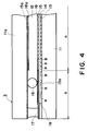
- Figure 4 is a sectional view of the liquid crystal device taken along line A-A in Figure 3.
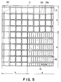
- Figure 5 is a plan view of a liquid crystal device according to a second embodiment of the present invention.
- Figure 6 is a plan view of a liquid crystal device according to a third embodiment of the present invention.
- the liquid crystal device is characterized by providing at least one substrate with a first electrode group at least in an effective optical modulation region and a second electrode (group) in peripheral region, whereby a cell gap is uniformized in the entire region where a liquid crystal material is filled and an alignment state of the liquid crystal material can be controlled uniformly in the entire region including the effective optical modulation region and the peripheral region.
- the second electrode located in the peripheral region is apart (separated) from the first electrode located in the effective optical modulation region.
- the second electrode functions as a dummy electrode which is not actuated or supplied with an voltage, thus failing to contribute to control of alignment (orientation) direction (e.g., switching) of liquid crystal molecules.
- the second (dummy) electrode is effective in preventing an adverse influence of a short-circuit occurred in the peripheral region on the effective optical modulation region since the second electrode is separated (insulated) from the first (or display) electrode formed in the effective optical modulation region.
- an optical modulation region means a display region having a prescribed display area in which a transmittance of a large number of pixels is controlled by using an applied drive signal to effect display in the case of a display device or means a region having a prescribed optical modulation area in which appropriate optical modulation is performed depending on drive signals in the case of a non-display device (a device other than the display device).
- peripheral region means at least one region which does not substantially contribute to optical modulation (e.g., control of transmittance) and disposed outside the effective optical modulation region.
- the peripheral region may preferably comprise two regions opposite to each other via the effective optical modulation.
- the peripheral region may more preferably enclose (surround) the effective optical modulation region on all (four) sides thereof.
- an electrode (group) is formed in not only the effective optical modulation region but also the peripheral region.
- a layer of an electrode material formed in the above manner is patterned by etching treatment in both the regions to provide a prescribed pattern.
- the thus patterned electrode is not removed by the etching treatment but remains in the peripheral region, whereby the penetration of a specific ion, e.g., chlorine ion, contained in the etchant used in the etching treatment into the lower layer(s) closer to the substrate can be suppressed.
- an adverse influence of a (peeling) solution for removing a resist pattern used in the above patterning step of the electrode upon the lower layer(s) can also be prevented.
- an impurity ion such as sodium ion
- the impurity ion is prevented from reacting with an ion (e.g., chlorine ion) contained in the etchant, thus preventing an occurrence of a defect, such as the peeling of the layer(s) located closer to the substrate.
- an electrode (first electrode) formed on a substrate in the effective optical modulation region may preferably have a prescribed pattern corresponding to display pixels.
- an electrode (second electrode) formed on the (identical) substrate in the peripheral region may preferably have a prescribed pattern in view of, e.g., a capacity (or capacitance) between the substrates.
- the electrode patterns in the above two regions may appropriately be formed to have the same or different shapes in view of a degree of control of, e.g., a gap between the substrates.
- the second electrode formed in the peripheral region may preferably have a pattern having a size, with respect to each electrode segment, larger than that of a pattern of the first electrode formed in the effective optical modulation region in order to suppress the peeling of the second electrode.
- the above structural features of the (transparent) electrodes formed on the substrate(s) may also be applied to an auxiliary electrode optionally disposed on or outside of the electrodes in order to control a resistance of the electrodes as a whole (i.e., the auxiliary electrode(s) may be disposed both in the above two regions and may be patterned in a prescribed shape).
- the liquid crystal device may preferably he a color liquid crystal display device.
- An ordinary color liquid crystal display device includes a group of color filter films comprising color filter segments of red (R), green (G) and blue (B), and optional white (transparent) (W) as desired, each containing corresponding colored resins, respectively, in at least the effective optical modulation region (display region) on one of a pair of substrates.
- the color filter segments may appropriately be patterned and combined with each other to constitute one (display) pixel.
- a transparent (flat) layer for flattening an unevenness (irregularity) of the color filter films is formed, and thereon a pattern of a group of transparent electrodes comprising an electroconductive transparent material (e.g., ITO) is formed in accordance with one pixel or the color filter segment(s) constituting one pixel.
- an electroconductive transparent material e.g., ITO
- the color liquid crystal display device has a group of patterned transparent electrodes formed not only in the effective optical modulation region (display region) but also in the peripheral (non-display) region.
- the group of patterned transparent electrode may preferably be formed via a group of color filter films as a dummy color filter and a transparent layer successively formed in this order on the substrate.
- the group of (dummy) color filter films may have a pattern similar to or different from that of the group of color filter films formed within the display region.
- the group of (dummy) color filter films formed in the peripheral region may preferably be patterned so as to have a size, with respect to each of color filter segments, larger than that of a pattern of the group of color filter films formed in the display region.
- the presence of the group of transparent electrodes in the display and peripheral regions is very effective in preventing the peeling of the group of color filter film and/or the transparent layer as described above.
- a liquid crystal material may include a pneumatic liquid crystal, a smectic liquid crystal including a chiral smectic liquid crystal (e.g., a ferroelectric liquid crystal) and other liquid crystals. These materials may be used singly or mixture (composition) of two or more species.
- the above liquid crystal is disposed between the pair of substrate with a prescribed cell gap.
- the above-mentioned layer structure on the substrate may suitably be applied to a liquid crystal device having ai smaller cell gap.
- a liquid crystal device using a chiral smectic (ferroelectric) liquid crystal is set to have a very small cell gap of at most 5 ⁇ m, preferably 0.5 - 2 ⁇ m, particularly about 1 ⁇ m, so that it is important to control uniformity of the cell gap.
- the above layer structure i.e., a layer structure wherein a group of color filter films, transparent layer, and a group of transparent electrodes are formed in this order on a substrate in both of the effective optical modulation region and the peripheral region may preferably be adopted in the present invention.
- Figures 3 and 4 show a first embodiment of the liquid crystal device of the present invention, wherein Figure 3 is a plan view of one substrate and Figure 4 is a sectional view of the entire device structure taken along line A-A in Figure 3.
- a liquid crystal device 3 includes a pair of substrates 11 and 11a each comprising a sheet (or flat) glass.
- a group of color filter films 13 comprising color filter segments of red (R), green (G) and blue (B) each containing respective colored resins is formed in a region corresponding to an effective optical modulation region (display region) a and a group of color filter films 13a comprising color filter segments (R, G and B) is formed in a region which corresponds to a peripheral region b but is inside the periphery of the device where the two substrates 11 and 11b are sealed with a sealing agent 17.
- Examples of a material for the color filter films may include a photosensitive resin (e.g., polyamide or polyimide) containing pigments for respective colors dispersed therein.
- the group of color filter films 13a (in the peripheral region a ) has a dummy pattern different from a pattern of the group of color filter films 13 (in the display region b) in this embodiment but may have a dummy pattern identical to a pattern of the group of color filter films 13.
- a coating (flat) layer 14 comprising a transparent resin is formed to flatten or smooth an unevenness (irregularity) in thickness (height) of respective color filter segments (S, G and B) are recesses therebetween.
- a group of transparent electrodes 15 in the form of stripes for applying a voltage to a liquid crystal layer is formed in the display region a and a grope of transparent electrodes 19 is formed in the peripheral region b and extends to the edge of the substrate 11.
- the group of transparent electrodes 19 is apart (separated) from the group of transparent electrodes 15 so as not to contribute to drive of the device.
- an insulating film 18 comprising a polymeric material or an inorganic material and subjected to uniaxial aligning treatment (e.g., rubbing) is formed.
- a group of transparent electrodes 15 in the form of stripes is formed in the display region a . Further, on the group of transparent electrodes 15 and the substrate 11a, an insulating film 18a (similar to the insulating film 18) is formed.
- a spacer 16 is disposed between the opposite insulating films 18 and 18a to provide a prescribe cell gap filled with a liquid crystal 12.
- a light-interrupting layer may appropriately be disposed in the display region a in a prescribed pattern between or among a prescribed number of color filter segments 13 at the same level in order to prevent unnecessary color mixing therebetween.
- the light-interrupting layer may preferably extend to the peripheral region.
- an auxiliary electrode e.g., comprising a metal material
- the group of transparent electrodes 15 is electrically connected with an external drive unit, such as a driving IC (integrated circuit) disposed outside of the device 3 (not shown in Figures 3 and 4).
- the respective stripe electrodes 15 may be connected with a driving IC on the same side or an different sides each other.
- the stripe electrode 15 is also formed in the peripheral region b, but is not connected, a corresponding transparent electrode 19 apart from the stripe electrode 15 is disposed in the opposite peripheral region b. For this reason, the electrodes 15 and 19 formed on the same substrate 11, as a whole, provided a uniform cell gap between the substrates 11 and 11a over the regions a and b.
- the respective structural members are formed or prepared as follows.
- Each of the group of color filter films 13 and 13a disposed in the regions a and b, respectively, is formed on the glass substrate 11 in the following manner.
- a solution containing a color filter-forming material principally comprising a photosensitive resin for one color filter is applied onto the substrate 11 and pre-dried (pre-baked) on a hot plate.
- the resultant substrate 11 is subjected to photo-curing (or -setting) (exposure with light) with a photomask to cure a necessary part (exposed part) of the photosensitive resin, followed by removal of an unnecessary part (unexposed part) of the photosensitive resin through development.
- the thus treated substrate 11 is further subjected to curing (post-baking) with the hot plate to obtain a single color (e.g., red) color filter film.
- the above steps are repeated two times with respect to photosensitive resins for the remaining two color filters (e.g., green and blue), respectively, in this order, and optionally repeated with respect to a photosensitive resin for white (transparent) color filter, as desired, to provide an objective group of color filter film comprising color filter segments of at least three colors (red (R), green (G), blue (B) and optional white (W)) to the substrate 11.
- a photosensitive resin for white (transparent) color filter as desired, to provide an objective group of color filter film comprising color filter segments of at least three colors (red (R), green (G), blue (B) and optional white (W)) to the substrate 11.
- a solution containing a transparent resin is applied onto the above prepared substrate 11 by spinner coating and dried and cured (baked) with the hot plate to form a coating (flat) layer 14 on the above substrate 11.
- an electroconductive transparent film e.g., ITO film
- a photoresist having prescribed pattern is formed on the electroconductive transparent film by a photolithographic process and subjected to etching with an etchant containing, e.g., chlorine ion, such as a mixture solution of hydroiodic (or hydrochloric) acid and ferric chloride, followed by peeling-off of the photoresist to form a group of transparent electrodes 14 (e.g., in the form of stripes) in the display region a (and partially in the peripheral region b) and a group of transparent electrodes 19 (e.g., in the form of stripes) in the peripheral region b.
- an etchant containing, e.g., chlorine ion, such as a mixture solution of hydroiodic (or hydrochloric) acid and ferric chloride
- an insulating film 18 comprising at least one layer is formed at least on the electrode 15 by using a vacuum film-forming apparatus or according to printing process, optionally followed by uniaxial aligning treatment, such as rubbing.
- a group of transparent electrodes 15a and an insulating film 18a are successively formed on the other substrate 11a in the same manner as above.
- the thus prepared two substrates 11 and 11a are oppositely applied to each other via a spacer 16 by using a sealing agent 17 at the periphery thereof so as to leave an injection port of a liquid crystal.
- a liquid crystal 12 is then injected into a cell gap (a gap between the substrates 11 and 11a) through the injection port, followed by sealing of the injection port.
- a resultant liquid crystal cell is subjected to aligning treatment including heating to prepare a liquid crystal device according to this embodiment as shown in Figure 4.
- liquid crystal device (as shown in Figure 4) is prepared by using the following structural members and under the following conditions.
- the above-prepared liquid crystal device according to this embodiment did not cause a peeling phenomenon of the transparent layer 14 and the color filter films 13 and 13a at all and provided no alignment defect even at the boundary between the display (effective optical modulation) region a and the peripheral region b.
- a liquid crystal device has the same cell structure as that of the first embodiment ( Figure 3) except that a group of transparent electrode 20 is patterned in the form of independent squares each having a size slightly larger than that of each color filter segment 13a.
- the liquid crystal device in this embodiment also has a uniform cell gap over the entire region (including the regions a and b). Further, in the both regions a and b, the liquid crystal shows a uniform alignment state.
- a liquid crystal device has the same cell structure as that of the second embodiment ( Figure 5) except that a light-interrupting layer 21 in the form of stripes as shown in Figure 6 is disposed between the color filter films 13 in a region corresponding to a space between the stripe transparent electrodes 15 in the region a and partially between those 20 in the region b and that a group of transparent electrodes 20 are partially patterned in the form of independent squares similar to those in Figure 5 but having a larger spacing in a region b' and partially patterned in the form of stripes (each including three squares in the figure) in the region b but in a region adjacent to a region corresponding to the region where the light-interrupting layer 21 is formed.
- the liquid crystal device similarly as in the first and second embodiments, has a cell gap with a good uniformity in not only the display region a but also the peripheral regions b and b'. Further, in these regions a , b and b', the liquid crystal shows a uniform alignment state.
- a liquid crystal device having the above-described structure was prepared in the same manner as in the second embodiment except that a light-interrupting layer 21 having a thickness of about 1000 A was additionally formed by using an alloy of Mo-Ta.
- a liquid crystal device having a uniform cell gap and showing a good display characteristic free from defects by providing at least one substrate with a first electrode in an effective optical modulation region and a second electrode in a peripheral region separated from each other.
- the above electrode arrangement is more effective in improving a display quality by suppressing peeling of the color filter film and the coating layer particularly in the peripheral region and providing a uniform liquid crystal layer thickness.
- a liquid crystal device is constituted by disposing a liquid crystal between a pair of substrates each provided with an electrode to provide an effective optical modulation region and a peripheral region.
- At least one substrate of the pair of substrates comprises an intermediate layer disposed between the substrate and the electrode in the effective optical modulation region and the peripheral region, and the electrode on the intermediate layer comprises a first electrode disposed at least in the effective optical modulation region and a second electrode disposed in the peripheral region.
- the first and second electrodes are separated from each other.
- the intermediate layer may preferably include a color filter, a light-interrupting layer and a coating layer.
Abstract
Description
- The present invention relates a liquid crystal device, particularly a liquid crystal device equipped with a color filter, and a process for producing the liquid crystal device.
- There has been known a liquid crystal device comprising a pair of substrates each provided with an electrode and a liquid crystal disposed between the substrates. The liquid device performs optical modulation by applying a voltage to the liquid crystal to applying a voltage to the liquid crystal to control alignment (or orientation) of liquid crystal molecules. Particularly, liquid crystal display devices wherein alignment of liquid crystal molecules is controlled by applying a voltage in accordance with image data (image information) to form a display image has arrested attention as flat panel displays in place of display devices using a cathode-ray tube (CRT). Of these devices, there has been actively developed a color liquid crystal panel including: a pair of substrates on one of which substrates a color filter film portion comprising at least three color films of red (R), green (G) and blue (B); electrodes as light switches each corresponding to respective color films; and a liquid crystal disposed between the substrates.
- Some embodiments of such a color liquid crystal device will be described with reference to Figures 1 and 2.
- Figure 1 shows an embodiment of a color liquid
crystal display device 4 including a pair ofsubstrates spacer 46 and aliquid crystal 42 filling the gap and sandwiched between thesubstrates device 4 has an effective optical modulation region a comprising a plurality of display pixels (picture elements) constituting a display region and also has a peripheral region b located outside of and in contact with the effective optical modulation region a. In the region a, a group ofcolor filter films 43 comprising three color films containing corresponding colored resins of red (R), green (G) and blue (B), respectively and a flat (or even) layer orfilm 44 comprising a transparent resin as a main component for coating (or covering) the group ofcolor filter films 43 and for flattening the resultant surface are successively formed on at least one of the substrates (on thesubstrate 41 in this embodiment). On theflat layer 44, a group of pluraltransparent electrodes 45 having a prescribed pattern corresponding to display pixels in order to drive the liquid crystal display device is formed. On theother substrate 41a, a group of pluraltransparent electrode 45a having a prescribed pattern corresponding to display pixels are formed. In this embodiment, display pixels are formed at intersections of the groups oftransparent electrodes transparent electrodes - On the other hand, the peripheral region b is not a region contributing to optical modulation. In the region b, however, in order to provide good optical modulation characteristics in the above-described region a the
flat layer 44 is continuously formed on thesubstrate 41, i.e., extends from the region a to the region b, so that a gap between thesubstrates - The
substrates sealing agent 47 as an end portion (in the region b in this embodiment). - Figure 2 shows another embodiment of a color liquid crystal display device principally having the similar cell structure as in Figure 1. In Figure 2, identical structural members (or elements) are shown by identical reference numerals used in the device of Figure 1 described above. In this embodiment, however, insulating films (alignment control films) 49 and 49a having been subjected to uniaxial aligning treatment are formed on the groups of
transparent electrodes substrates filter film portion 43a is formed on thesubstrate 41. On the colorfilter film portion 43a, theflat film 44 andinsulating film 48 are successively formed and each continuously extends from the region a to the region b. On theother substrate 41a, the insulating film 48a which continuously extends from the region a to the region b is formed. - However, in the above-mentioned liquid crystal devices as shown in Figures 1 and 2, the gap between the substrates (i.e., cell gap or the thickness of liquid crystal layer) is not uniformized sufficiently in the regions a and b as a whole, thus failing to effect uniform control of an alignment state of liquid crystal molecules over the entire liquid crystal panel. Particularly, the alignment state in the vicinity of an end portion of the effective optical modulation region a is liable to become ununiform.
- Further, the liquid crystal devices as shown in Figures 1 and 2 are liable to cause defects resulting from an electrode substrate production process and materials used therefor.
- More specifically, the production (or preparation) of respective substrate constituting the liquid crystal device, particularly that of the
substrate 41 equipped with the group of color filter films may be performed as follows. A group ofcolor filter films flat film 44 is formed on the entire surface of thesubstrate 41 provided with the group ofcolor filter films flat film 44 by, e.g., vacuum vapor deposition. On the electroconductive (transparent) film, a prescribed resist pattern as a mask is formed according to a photolithographic process, followed by etching to form a group ofelectrodes 45 having a prescribed pattern in a region corresponding to the effective optical modulation region a. Further, aninsulating film 48 is formed on theentire electrodes 45, as desired. - In the etching step of the electroconductive transparent film in the above production process, a chlorine ion-containing solution, such as a hydroiodic acid-ferric chloride mixture solution or a hydrochloric acid-ferric chloride mixture solution is used as an etchant (etching solution). In this case, however, in the peripheral region b where the electroconductive transparent film is completely removed, chlorine ions in the etchant penetrate through the
flat film 44 and thecolor filter film 43a having been disposed under the electroconductive transparent film to reach and remain at the surface of thesubstrate 41 during and after the etching step. On the other hand, sodium ions are provided on thesubstrate 41 in a heating step after the etching step, e.g., a hot (heat) curing step of forming aninsulating film 48 as an upper layer or a heating step at 200 oC or above in the aligning treatment of a liquid crystal material. As a result, in the above heating step, the chlorine ion and the sodium ion react with each other to precipitate sodium chloride, whereby theflat film 44 and/or thecolor filter film 43a located lower than the electrode are liable to be peeled off. This phenomenon also adversely affects the layers formed in the effective modulation region a and those formed on thesubstrate 41a free from the color filter film in case where some film or layer is formed under the electrode according to necessity. - In order to remedy the above difficulties, a high-purity glass plate having a low or no impurity content (e.g., sodium content) is tried to be used as a substrate or a barrier layer formed under the color filter film or formed on the flat film is tried to prevent the penetration of and reaction of the chlorine ion with the sodium ion.
- However, at the present status, sufficient effects cannot be attained and a complicated production process is necessitated, thus leaving room for improvement.
- An object of the present invention is to provide a liquid crystal device, including a pair of substrates each provided with an electrode and a liquid crystal sandwiched between the substrate, providing a uniform gap or spacing between the substrates (i.e., cell gap or liquid crystal layer thickness) over the entire region of the device to allow uniform and good alignment state of liquid crystal molecules in the entire region and preventing peeling of a layer in lamination layer structure of a substrate, particularly in a region other than an effective optical modulation region, to suppress an occurrence of a defect in a resultant device, such as an alignment defect.
- Another object of the present invention is to provide a process for producing the liquid crystal device described above.
- According to the present invention, there is provided a liquid crystal device, comprising: a pair of substrates each provided with an electrode, and a liquid crystal disposed between the pair of substrates to provide an effective optical modulation region and a peripheral region, wherein
at least one substrate of the pair of substrates comprises an intermediate layer disposed between the substrate and the electrode in the effective optical modulation region and the peripheral region, and the electrode on the intermediate layer comprises a first electrode disposed at least in the effective optical modulation region and a second electrode disposed in the peripheral region, the first and second electrodes being separated from each other. - According to the present invention, there is also provided a liquid crystal device, comprising: a pair of substrates each provided with an electrode, and a liquid crystal disposed between the pair of substrates to provide an effective optical modulation region and a peripheral region, wherein
at least one substrate of the pair of substrates has an effective optical modulation region and a peripheral region including a first region and a second region disposed opposite to each other with respect to the effective optical modulation region, and
the electrode on said at least one substrate has a first pattern in the form of stripes extending from the effective optical modulation region to a an outside portion via the second region to be connected with an external drive unit and has a second pattern in the first region apart from the first pattern. - According to the present invention, there is further provided a process for producing a liquid crystal device comprising a pair of substrates each provided with an electrode, and a liquid crystal disposed between the pair of substrates to provide an effective optical modulation region and a peripheral region; including the steps of:
- forming an intermediate layer on at least one substrate of the pair of substrates in the effective optical modulation region and the peripheral region, and
- forming on the intermediate layer an electrode having a first electrode pattern in the effective optical modulation region and a second electrode pattern in the peripheral region through a photolithographic process and an etching with an etchant.
- These and other objects, features and advantages of the present invention will become more apparent upon a consideration of the following description of the preferred embodiments of the present invention taken in conjunction with the accompanying drawings.
- Figure 1 is a sectional view of an embodiment of a liquid crystal device.
- Figure 2 is a sectional view of another embodiment of a liquid crystal device.
- Figure 3 is a plan view of a liquid crystal device according to a first embodiment of the present invention.
- Figure 4 is a sectional view of the liquid crystal device taken along line A-A in Figure 3.
- Figure 5 is a plan view of a liquid crystal device according to a second embodiment of the present invention.
- Figure 6 is a plan view of a liquid crystal device according to a third embodiment of the present invention.
- The liquid crystal device according to the present invention is characterized by providing at least one substrate with a first electrode group at least in an effective optical modulation region and a second electrode (group) in peripheral region, whereby a cell gap is uniformized in the entire region where a liquid crystal material is filled and an alignment state of the liquid crystal material can be controlled uniformly in the entire region including the effective optical modulation region and the peripheral region.
- The second electrode located in the peripheral region is apart (separated) from the first electrode located in the effective optical modulation region. In a preferred embodiment, the second electrode functions as a dummy electrode which is not actuated or supplied with an voltage, thus failing to contribute to control of alignment (orientation) direction (e.g., switching) of liquid crystal molecules. The second (dummy) electrode is effective in preventing an adverse influence of a short-circuit occurred in the peripheral region on the effective optical modulation region since the second electrode is separated (insulated) from the first (or display) electrode formed in the effective optical modulation region.
- Herein "effective optical modulation region" means a display region having a prescribed display area in which a transmittance of a large number of pixels is controlled by using an applied drive signal to effect display in the case of a display device or means a region having a prescribed optical modulation area in which appropriate optical modulation is performed depending on drive signals in the case of a non-display device (a device other than the display device). Further, "peripheral region" means at least one region which does not substantially contribute to optical modulation (e.g., control of transmittance) and disposed outside the effective optical modulation region. The peripheral region may preferably comprise two regions opposite to each other via the effective optical modulation. The peripheral region may more preferably enclose (surround) the effective optical modulation region on all (four) sides thereof.
- In the liquid crystal device according to the present invention, an electrode (group) is formed in not only the effective optical modulation region but also the peripheral region. Taking a general (substrate) production process of the liquid crystal device into consideration, as a result, a layer of an electrode material formed in the above manner is patterned by etching treatment in both the regions to provide a prescribed pattern. In this instance, the thus patterned electrode is not removed by the etching treatment but remains in the peripheral region, whereby the penetration of a specific ion, e.g., chlorine ion, contained in the etchant used in the etching treatment into the lower layer(s) closer to the substrate can be suppressed. Further, an adverse influence of a (peeling) solution for removing a resist pattern used in the above patterning step of the electrode upon the lower layer(s) can also be prevented. Even if an impurity ion, such as sodium ion, is generated on the substrate surface in a post-treatment (e.g., hot curing of a resultant film or heating for aligning treatment of a liquid crystal), the impurity ion is prevented from reacting with an ion (e.g., chlorine ion) contained in the etchant, thus preventing an occurrence of a defect, such as the peeling of the layer(s) located closer to the substrate.
- In case where the liquid crystal device of the present invention is used as a display device, an electrode (first electrode) formed on a substrate in the effective optical modulation region may preferably have a prescribed pattern corresponding to display pixels. Similarly, an electrode (second electrode) formed on the (identical) substrate in the peripheral region may preferably have a prescribed pattern in view of, e.g., a capacity (or capacitance) between the substrates. In a more preferred embodiment, the electrode patterns in the above two regions may appropriately be formed to have the same or different shapes in view of a degree of control of, e.g., a gap between the substrates. Particularly, the second electrode formed in the peripheral region may preferably have a pattern having a size, with respect to each electrode segment, larger than that of a pattern of the first electrode formed in the effective optical modulation region in order to suppress the peeling of the second electrode. The above structural features of the (transparent) electrodes formed on the substrate(s) may also be applied to an auxiliary electrode optionally disposed on or outside of the electrodes in order to control a resistance of the electrodes as a whole (i.e., the auxiliary electrode(s) may be disposed both in the above two regions and may be patterned in a prescribed shape).
- In the present invention, the liquid crystal device may preferably he a color liquid crystal display device.
- An ordinary color liquid crystal display device includes a group of color filter films comprising color filter segments of red (R), green (G) and blue (B), and optional white (transparent) (W) as desired, each containing corresponding colored resins, respectively, in at least the effective optical modulation region (display region) on one of a pair of substrates. The color filter segments may appropriately be patterned and combined with each other to constitute one (display) pixel. On the patterned color filter films, a transparent (flat) layer for flattening an unevenness (irregularity) of the color filter films is formed, and thereon a pattern of a group of transparent electrodes comprising an electroconductive transparent material (e.g., ITO) is formed in accordance with one pixel or the color filter segment(s) constituting one pixel.
- In the present invention, the color liquid crystal display device has a group of patterned transparent electrodes formed not only in the effective optical modulation region (display region) but also in the peripheral (non-display) region. In this case, also in the peripheral region, the group of patterned transparent electrode may preferably be formed via a group of color filter films as a dummy color filter and a transparent layer successively formed in this order on the substrate. The group of (dummy) color filter films may have a pattern similar to or different from that of the group of color filter films formed within the display region. However, the group of (dummy) color filter films formed in the peripheral region may preferably be patterned so as to have a size, with respect to each of color filter segments, larger than that of a pattern of the group of color filter films formed in the display region. In the above (plural)-layer structure on the substrate, the presence of the group of transparent electrodes in the display and peripheral regions is very effective in preventing the peeling of the group of color filter film and/or the transparent layer as described above.
- In the present invention, a liquid crystal material may include a pneumatic liquid crystal, a smectic liquid crystal including a chiral smectic liquid crystal (e.g., a ferroelectric liquid crystal) and other liquid crystals. These materials may be used singly or mixture (composition) of two or more species.
- The above liquid crystal is disposed between the pair of substrate with a prescribed cell gap. The above-mentioned layer structure on the substrate may suitably be applied to a liquid crystal device having ai smaller cell gap. Particularly, a liquid crystal device using a chiral smectic (ferroelectric) liquid crystal is set to have a very small cell gap of at most 5 µm, preferably 0.5 - 2 µm, particularly about 1 µm, so that it is important to control uniformity of the cell gap. For this reason, the above layer structure, i.e., a layer structure wherein a group of color filter films, transparent layer, and a group of transparent electrodes are formed in this order on a substrate in both of the effective optical modulation region and the peripheral region may preferably be adopted in the present invention.
- Hereinbelow, some preferred embodiments of the liquid crystal device according to the present invention will be described with reference to Figures 3 - 6 in which identical structural members and regions are indicated by identical reference numerals.
- Figures 3 and 4 show a first embodiment of the liquid crystal device of the present invention, wherein Figure 3 is a plan view of one substrate and Figure 4 is a sectional view of the entire device structure taken along line A-A in Figure 3.
- Referring to Figures 3 and 4, a
liquid crystal device 3 includes a pair ofsubstrates 11 and 11a each comprising a sheet (or flat) glass. On onesubstrate 11, a group ofcolor filter films 13 comprising color filter segments of red (R), green (G) and blue (B) each containing respective colored resins is formed in a region corresponding to an effective optical modulation region (display region) a and a group ofcolor filter films 13a comprising color filter segments (R, G and B) is formed in a region which corresponds to a peripheral region b but is inside the periphery of the device where the twosubstrates 11 and 11b are sealed with a sealingagent 17. Examples of a material for the color filter films may include a photosensitive resin (e.g., polyamide or polyimide) containing pigments for respective colors dispersed therein. The group ofcolor filter films 13a (in the peripheral region a) has a dummy pattern different from a pattern of the group of color filter films 13 (in the display region b) in this embodiment but may have a dummy pattern identical to a pattern of the group ofcolor filter films 13. On the group ofcolor filter films layer 14 comprising a transparent resin is formed to flatten or smooth an unevenness (irregularity) in thickness (height) of respective color filter segments (S, G and B) are recesses therebetween. On thecoating layer 14, a group oftransparent electrodes 15 in the form of stripes for applying a voltage to a liquid crystal layer is formed in the display region a and a grope oftransparent electrodes 19 is formed in the peripheral region b and extends to the edge of thesubstrate 11. The group oftransparent electrodes 19 is apart (separated) from the group oftransparent electrodes 15 so as not to contribute to drive of the device. On the groups oftransparent electrodes film 18 comprising a polymeric material or an inorganic material and subjected to uniaxial aligning treatment (e.g., rubbing) is formed. - On the other substrate 11a, a group of
transparent electrodes 15 in the form of stripes is formed in the display region a. Further, on the group oftransparent electrodes 15 and the substrate 11a, an insulating film 18a (similar to the insulating film 18) is formed. - Between the opposite insulating
films 18 and 18a, aspacer 16 is disposed to provide a prescribe cell gap filled with aliquid crystal 12. - In this embodiment, on the
substrate 11, a light-interrupting layer may appropriately be disposed in the display region a in a prescribed pattern between or among a prescribed number ofcolor filter segments 13 at the same level in order to prevent unnecessary color mixing therebetween. The light-interrupting layer may preferably extend to the peripheral region. Further, in order to lower a resistance of the respectivetransparent electrodes electrodes - The group of
transparent electrodes 15 is electrically connected with an external drive unit, such as a driving IC (integrated circuit) disposed outside of the device 3 (not shown in Figures 3 and 4). In this case, therespective stripe electrodes 15 may be connected with a driving IC on the same side or an different sides each other. Further, on the side where eachstripe electrode 15 is connected, thestripe electrode 15 is also formed in the peripheral region b, but is not connected, a correspondingtransparent electrode 19 apart from thestripe electrode 15 is disposed in the opposite peripheral region b. For this reason, theelectrodes same substrate 11, as a whole, provided a uniform cell gap between thesubstrates 11 and 11a over the regions a and b. - In this embodiment, the respective structural members (elements) are formed or prepared as follows.
- Each of the group of
color filter films glass substrate 11 in the following manner. - First, a solution containing a color filter-forming material principally comprising a photosensitive resin for one color filter (e.g., red) is applied onto the
substrate 11 and pre-dried (pre-baked) on a hot plate. Then, theresultant substrate 11 is subjected to photo-curing (or -setting) (exposure with light) with a photomask to cure a necessary part (exposed part) of the photosensitive resin, followed by removal of an unnecessary part (unexposed part) of the photosensitive resin through development. The thus treatedsubstrate 11 is further subjected to curing (post-baking) with the hot plate to obtain a single color (e.g., red) color filter film. The above steps are repeated two times with respect to photosensitive resins for the remaining two color filters (e.g., green and blue), respectively, in this order, and optionally repeated with respect to a photosensitive resin for white (transparent) color filter, as desired, to provide an objective group of color filter film comprising color filter segments of at least three colors (red (R), green (G), blue (B) and optional white (W)) to thesubstrate 11. - Then, in order to flatten the difference in height among respective color filter segments and fill the spacing therebetween, a solution containing a transparent resin is applied onto the above
prepared substrate 11 by spinner coating and dried and cured (baked) with the hot plate to form a coating (flat)layer 14 on theabove substrate 11. - Thereafter, an electroconductive transparent film (e.g., ITO film) is formed on the entire surface of the
coating layer 14 by using a vacuum film-forming apparatus. Subsequently, a photoresist having prescribed pattern (as a photomask) is formed on the electroconductive transparent film by a photolithographic process and subjected to etching with an etchant containing, e.g., chlorine ion, such as a mixture solution of hydroiodic (or hydrochloric) acid and ferric chloride, followed by peeling-off of the photoresist to form a group of transparent electrodes 14 (e.g., in the form of stripes) in the display region a (and partially in the peripheral region b) and a group of transparent electrodes 19 (e.g., in the form of stripes) in the peripheral region b. - Then, an insulating
film 18 comprising at least one layer is formed at least on theelectrode 15 by using a vacuum film-forming apparatus or according to printing process, optionally followed by uniaxial aligning treatment, such as rubbing. - On the other hand, a group of
transparent electrodes 15a and an insulating film 18a are successively formed on the other substrate 11a in the same manner as above. - The thus prepared two
substrates 11 and 11a are oppositely applied to each other via aspacer 16 by using a sealingagent 17 at the periphery thereof so as to leave an injection port of a liquid crystal. Aliquid crystal 12 is then injected into a cell gap (a gap between thesubstrates 11 and 11a) through the injection port, followed by sealing of the injection port. Thereafter, a resultant liquid crystal cell is subjected to aligning treatment including heating to prepare a liquid crystal device according to this embodiment as shown in Figure 4. - More specifically, the above liquid crystal device (as shown in Figure 4) is prepared by using the following structural members and under the following conditions.
- Substrate (11, 11a): sheet (or flat) glass (thickness = 1.1 mm)
- Color filter film (13, 13a): three color filter segments of R, G and B (thickness = c.a. 2 µm)
- Coating film (14): transparent resin (thickness = c.a. 3 µm)
- Transparent electrode (15, 15a, 19): ITO film (thickness = c.a. 0.1 µm)
- Liquid crystal (12): chiral smectic liquid crystal (mixture)
- Cell gap: 1.1 µm (average value)
- Etchant used: hydrochloric acid/ferric chloride mixture solution (3/2 by volume)
- Aligning treatment (of liquid crystal): including heating for 1 hour at 270 oC
- The above-prepared liquid crystal device according to this embodiment did not cause a peeling phenomenon of the
transparent layer 14 and thecolor filter films - With reference to Figure 5, a second embodiment of the liquid crystal device of the present invention will be described.
- Referring to Figure 5, a liquid crystal device according to this embodiment has the same cell structure as that of the first embodiment (Figure 3) except that a group of
transparent electrode 20 is patterned in the form of independent squares each having a size slightly larger than that of eachcolor filter segment 13a. Similarly as in the first embodiment, the liquid crystal device in this embodiment also has a uniform cell gap over the entire region (including the regions a and b). Further, in the both regions a and b, the liquid crystal shows a uniform alignment state. - A liquid crystal device having the above-described structure as shown in Figure 5 was prepared in the same manner as in the first embodiment except for using an etchant (for patterning transparent electrodes) comprising a mixture solution (hydroiodic acid/ferric chloride = 3/2 by volume).
- As a result, similarly as in the first embodiment, peeling of the
coating film 14 and thecolor filter film 13a liable to be caused in the peripheral region b was not observed at all and excellent display characteristics were confirmed. - Then, a third embodiment of the liquid crystal device according to the present invention will be explained with reference to Figure 6.
- Referring to Figure 6, a liquid crystal device according to this embodiment has the same cell structure as that of the second embodiment (Figure 5) except that a light-interrupting
layer 21 in the form of stripes as shown in Figure 6 is disposed between thecolor filter films 13 in a region corresponding to a space between the stripetransparent electrodes 15 in the region a and partially between those 20 in the region b and that a group oftransparent electrodes 20 are partially patterned in the form of independent squares similar to those in Figure 5 but having a larger spacing in a region b' and partially patterned in the form of stripes (each including three squares in the figure) in the region b but in a region adjacent to a region corresponding to the region where the light-interruptinglayer 21 is formed. In this embodiment, similarly as in the first and second embodiments, the liquid crystal device has a cell gap with a good uniformity in not only the display region a but also the peripheral regions b and b'. Further, in these regions a, b and b', the liquid crystal shows a uniform alignment state. - A liquid crystal device having the above-described structure was prepared in the same manner as in the second embodiment except that a light-interrupting
layer 21 having a thickness of about 1000 A was additionally formed by using an alloy of Mo-Ta. - As a result, similarly as in the second embodiment, peeling of the
coating film 14 and thecolor filter film 13a liable to be caused in the peripheral regions b and b' was not observed at all and excellent display characteristics were confirmed. - As described hereinabove, according to the present invention, there is provided a liquid crystal device having a uniform cell gap and showing a good display characteristic free from defects by providing at least one substrate with a first electrode in an effective optical modulation region and a second electrode in a peripheral region separated from each other.
- Particularly, in a color liquid crystal display device including a color filter film and a coating layer thereof and optionally a light-interrupting layer, the above electrode arrangement is more effective in improving a display quality by suppressing peeling of the color filter film and the coating layer particularly in the peripheral region and providing a uniform liquid crystal layer thickness.
- A liquid crystal device is constituted by disposing a liquid crystal between a pair of substrates each provided with an electrode to provide an effective optical modulation region and a peripheral region. At least one substrate of the pair of substrates comprises an intermediate layer disposed between the substrate and the electrode in the effective optical modulation region and the peripheral region, and the electrode on the intermediate layer comprises a first electrode disposed at least in the effective optical modulation region and a second electrode disposed in the peripheral region. The first and second electrodes are separated from each other. The intermediate layer may preferably include a color filter, a light-interrupting layer and a coating layer.
Claims (30)
- A liquid crystal device, comprising: a pair of substrates each provided with an electrode, and a liquid crystal disposed between the pair of substrates to provide an effective optical modulation region and a peripheral region, wherein
at least one substrate of the pair of substrates comprises an intermediate layer disposed between the substrate and the electrode in the effective optical modulation region and the peripheral region, and the electrode on the intermediate layer comprises a first electrode disposed at least in the effective optical modulation region and a second electrode disposed in the peripheral region, the first and second electrodes being separated from each other. - A device according to Claim 1, wherein the first electrode has a pattern corresponding to plural display pixels in the effective optical modulation region as a display region.
- A device according to Claim 2, wherein the intermediate layer comprises a color filter film comprising at least one color filter segment and a coating layer disposed on the color filter film and is disposed on one of the pair of substrates.
- A device according to Claim 1, wherein the electrodes disposed on the pair of substrates comprise an electroconductive transparent material.
- A device according to Claim 1, wherein the pair of substrates are applied to each other with a sealing agent at a periphery portion therebetween to provide a prescribed cell gap, and under the sealing agent, the second electrode disposed in the peripheral region extends.
- A device according to Claim 3, wherein the color filter film comprises at least three color filter segments comprising a red color filter segment, a green color filter segment, and a blue color filter segment.
- A device according to Claim 1, wherein the first electrode and the second electrode have different patterns.
- A device according to Claim 1, wherein the second electrode disposed in the peripheral region is not supplied with a voltage.
- A device according to Claim 3, wherein the intermediate layer further comprises a light-interrupting layer disposed so as to fill a space between a prescribed number of color filter segments in the effective optical modulation region.
- A device according to Claim 3, wherein the intermediate layer further comprises a light-interrupting layer disposed so as to fill a space between a prescribed number of color filter segments in the effective optical modulation region and the peripheral region.
- A device according to Claim 3, wherein the color filter film comprises a first color filter film in the effective optical modulation region and a second color filter film in the peripheral region, the second color filter film comprising at least one color filter segment each of which is larger in size than that of at least one color filter segment constituting the first color filter film.
- A device according to Claim 5, wherein the prescribed cell gap is a cell gap of at most 5 µm.
- A device according to Claim 1, wherein the liquid crystal comprises a chiral smectic liquid crystal.
- A process for producing a liquid crystal device comprising a pair of substrates each provided with an electrode, and a liquid crystal disposed between the pair of substrates to provide an effective optical modulation region and a peripheral region; including the steps of:forming an intermediate layer on at least one substrate of the pair of substrates in the effective optical modulation region and the peripheral region, andforming on the intermediate layer an electrode having a first electrode pattern in the effective optical modulation region and a second electrode pattern in the peripheral region through a photolithographic process and an etching with an etchant.
- A process according to Claim 14, wherein the etchant comprises a mixture solution of hydroiodic acid and ferric chloride or a mixture solution of hydrochloric acid and ferric chloride.
- A process according to Claim 14, wherein the steps of forming the intermediate layer includes the steps of:forming a color filter film comprising at least one color filter segment on said at least one substrate, andforming a coating layer on the color filter film.
- A process according to Claim 14, wherein the step of forming the intermediate layer includes the steps of:forming a color filter film comprising at least one color filter segment on said at least one substrate,forming a light-interrupting layer so as to fill a space between a prescribed number of color filter segments in the effective optical modulation region and the peripheral region, andforming a coating layer on the light-interrupting layer and the color filter film.
- A process according to Claim 14, wherein the first electrode pattern and the second electrode pattern are separated from each other.
- A liquid crystal device, comprising: a pair of substrates each provided with an electrode, and a liquid crystal disposed between the pair of substrates to provide an effective optical modulation region and a peripheral region, wherein
at least one substrate of the pair of substrates has an effective optical modulation region and a peripheral region including a first region and a second region disposed opposite to each other with respect to the effective optical modulation region, and
the electrode on said at least one substrate has a first pattern in the form of stripes extending from the effective optical modulation region to an outside portion via the second region to be connected with an external drive unit and has a second pattern in the first region apart from the first pattern. - A device according to Claim 19, wherein the second pattern comprises plural independent portions each of which is located in an extending direction of the corresponding stripe of the first pattern.
- A device according to Claim 19, wherein the electrode having the first and second patterns is formed on said at least one substrate via an intermediate layer disposed in the effective optical modulation region and the first and second regions of the peripheral region.
- A device according to Claim 19, wherein, in the effective optical modulation region, the electrodes of the pair of substrates have stripe patterns intersecting with each other to constitute plural display pixels.
- A device according to Claim 21, wherein the intermediate layer comprises a color filter film comprising at least one color filter segment, and in the effective optical modulation region, the electrodes of the pair of substrates have stripe patterns intersecting with each other to constitute plural display pixels.
- A device according to Claim 23, wherein the color filter film comprises at least three color filter segments comprising a red color filter segment, a green color filter segment, and a blue color filter segment.
- A device according to Claim 19, wherein the electrodes on the pair of substrates comprises an electroconductive transparent material.
- A device according to Claim 19, wherein the electrode having the second pattern is not supplied with a voltage in the first region.
- A device according to Claim 23, wherein the intermediate layer further comprises a light-interrupting layer disposed so as to fill a space between a prescribed number of color filter segments in the effective optical modulation region.
- A device according to Claim 23, wherein the intermediate layer further comprises a light-interrupting layer disposed so as to fill a space between a prescribed number of color filter segments in the effective optical modulation region and the first region of the peripheral region.
- A device according to Claim 19, wherein the liquid crystal device has a cell gap of at most 5 µm.
- A device according to Claim 19, wherein the liquid crystal comprises a chiral smectic liquid crystal.
Priority Applications (1)
| Application Number | Priority Date | Filing Date | Title |
|---|---|---|---|
| EP00120917A EP1069462B1 (en) | 1995-04-26 | 1996-04-25 | Liquid-crystal display |
Applications Claiming Priority (2)
| Application Number | Priority Date | Filing Date | Title |
|---|---|---|---|
| JP10222095 | 1995-04-26 | ||
| JP102220/95 | 1995-04-26 |
Related Child Applications (1)
| Application Number | Title | Priority Date | Filing Date |
|---|---|---|---|
| EP00120917A Division EP1069462B1 (en) | 1995-04-26 | 1996-04-25 | Liquid-crystal display |
Publications (3)
| Publication Number | Publication Date |
|---|---|
| EP0740182A2 true EP0740182A2 (en) | 1996-10-30 |
| EP0740182A3 EP0740182A3 (en) | 1998-03-11 |
| EP0740182B1 EP0740182B1 (en) | 2006-07-05 |
Family
ID=14321589
Family Applications (2)
| Application Number | Title | Priority Date | Filing Date |
|---|---|---|---|
| EP00120917A Expired - Lifetime EP1069462B1 (en) | 1995-04-26 | 1996-04-25 | Liquid-crystal display |
| EP96106568A Expired - Lifetime EP0740182B1 (en) | 1995-04-26 | 1996-04-25 | Liquid crystal device |
Family Applications Before (1)
| Application Number | Title | Priority Date | Filing Date |
|---|---|---|---|
| EP00120917A Expired - Lifetime EP1069462B1 (en) | 1995-04-26 | 1996-04-25 | Liquid-crystal display |
Country Status (3)
| Country | Link |
|---|---|
| US (1) | US5936694A (en) |
| EP (2) | EP1069462B1 (en) |
| DE (1) | DE69636318T2 (en) |
Cited By (3)
| Publication number | Priority date | Publication date | Assignee | Title |
|---|---|---|---|---|
| US6552764B2 (en) | 1998-07-28 | 2003-04-22 | Sharp Kabushiki Kaisha | Reflective LCD whose color filter pattern extends outside display region and whose seal overlaps color filter |
| EP1109052A3 (en) * | 1999-12-14 | 2004-06-09 | Alps Electric Co., Ltd. | Color filter substrate for reflective liquid crystal display and reflective liquid crystal display using the same |
| EP1930768A1 (en) * | 1997-06-12 | 2008-06-11 | Sharp Kabushiki Kaisha | Vertically-aligned (VA) liquid crystal display device |
Families Citing this family (24)
| Publication number | Priority date | Publication date | Assignee | Title |
|---|---|---|---|---|
| CN1137405C (en) * | 1996-08-31 | 2004-02-04 | 三星电管株式会社 | Flat-panel display device and mfg. method therefor |
| US6407793B1 (en) * | 2001-05-02 | 2002-06-18 | Giantplus Technology Co., Ltd. | Color liquid crystal display |
| JP4398602B2 (en) * | 2001-05-18 | 2010-01-13 | 株式会社日立製作所 | Liquid crystal display |
| EP1388818B1 (en) * | 2002-08-10 | 2011-06-22 | Samsung Electronics Co., Ltd. | Method and apparatus for rendering image signal |
| JP4191521B2 (en) * | 2003-03-28 | 2008-12-03 | アルゼ株式会社 | Game machine |
| FR2874447B1 (en) * | 2004-08-17 | 2007-01-12 | Nemoptic Sa | LIQUID CRYSTAL DISPLAY DEVICE COMPRISING ENHANCED SWITCHING MEANS AT THE PERIPHERY OF THE DISPLAY |
| US7898632B2 (en) * | 2005-12-28 | 2011-03-01 | Seiko Epson Corporation | Electro-optical device, manufacturing method thereof, and electronic apparatus |
| JP4207982B2 (en) * | 2006-06-15 | 2009-01-14 | エプソンイメージングデバイス株式会社 | LCD panel |
| US7884899B2 (en) * | 2007-02-02 | 2011-02-08 | Tpo Displays Corp. | System for displaying images and method with a peripheral region having a mosaic color filter pattern thereon that has pillars and channels and an opening along its boundary |
| US7679284B2 (en) * | 2007-02-08 | 2010-03-16 | Seiko Epson Corporation | Light emitting device and electronic apparatus |
| US20080251976A1 (en) * | 2007-04-13 | 2008-10-16 | Liquidia Technologies, Inc. | Micro and nano-spacers having highly uniform size and shape |
| CN101636687B (en) * | 2007-06-27 | 2011-12-21 | 夏普株式会社 | Liquid crystal display device and method for manufacturing the same |
| DE102007062944B4 (en) * | 2007-12-21 | 2016-03-17 | Leonhard Kurz Stiftung & Co. Kg | Electronic switch |
| TWI457875B (en) * | 2009-02-19 | 2014-10-21 | Prime View Int Co Ltd | Display device and method for fabricating the same |
| CN101840122B (en) * | 2009-03-19 | 2012-12-05 | 元太科技工业股份有限公司 | Display device and manufacturing method thereof |
| KR20130027189A (en) * | 2011-09-07 | 2013-03-15 | 삼성디스플레이 주식회사 | Liquid crystal display and method for manufacturing the same |
| US8582060B2 (en) | 2011-12-19 | 2013-11-12 | Japan Display West Inc. | Liquid crystal display panel |
| US9341878B2 (en) * | 2012-04-05 | 2016-05-17 | Apple Inc. | Displays with low reflectance border regions |
| JP6120064B2 (en) * | 2013-04-09 | 2017-04-26 | 日本精機株式会社 | Display device |
| CN105339835A (en) * | 2013-05-14 | 2016-02-17 | 苹果公司 | Displays with color filter material in border regions |
| TWI613492B (en) | 2017-05-05 | 2018-02-01 | 友達光電股份有限公司 | Color filter substrate and display panel |
| JP7378923B2 (en) * | 2018-10-31 | 2023-11-14 | キヤノン株式会社 | Semiconductor devices, modules, cameras and equipment |
| CN110310576B (en) * | 2019-06-29 | 2022-07-15 | 武汉天马微电子有限公司 | Display panel and display device |
| WO2021097715A1 (en) * | 2019-11-20 | 2021-05-27 | 京东方科技集团股份有限公司 | Display substrate, display panel, and display device |
Citations (4)
| Publication number | Priority date | Publication date | Assignee | Title |
|---|---|---|---|---|
| JPS62210425A (en) * | 1986-03-12 | 1987-09-16 | Hitachi Ltd | Liquid crystal display element |
| EP0338412A2 (en) * | 1988-04-21 | 1989-10-25 | Asahi Glass Company Ltd. | Color liquid crystal display device and method for driving same |
| JPH03211524A (en) * | 1990-01-17 | 1991-09-17 | Hitachi Ltd | Liquid crystal display element |
| EP0558058A1 (en) * | 1992-02-27 | 1993-09-01 | Canon Kabushiki Kaisha | Liquid crystal display device |
Family Cites Families (10)
| Publication number | Priority date | Publication date | Assignee | Title |
|---|---|---|---|---|
| JPS62229233A (en) * | 1986-03-31 | 1987-10-08 | Seiko Instr & Electronics Ltd | Liquid crystal display device |
| JPH0610702B2 (en) * | 1987-11-18 | 1994-02-09 | インターナショナル・ビジネス・マシーンズ・コーポレーション | Color liquid crystal display device and manufacturing method thereof |
| JPH01257823A (en) * | 1988-04-07 | 1989-10-13 | Dainippon Printing Co Ltd | Color filter substrate for liquid crystal display device |
| US5365357A (en) * | 1988-04-21 | 1994-11-15 | Asahi Glass Company Ltd. | Color liquid crystal display having color filters and light blocking layers in the periphery |
| US5191452A (en) * | 1989-09-20 | 1993-03-02 | Honeywell Inc. | Active matrix liquid crystal display fabrication for grayscale |
| FR2679057B1 (en) * | 1991-07-11 | 1995-10-20 | Morin Francois | LIQUID CRYSTAL, ACTIVE MATRIX AND HIGH DEFINITION SCREEN STRUCTURE. |
| US5317431A (en) * | 1991-11-21 | 1994-05-31 | Fujitsu Limited | Liquid crystal display device with scattering white layer and color filter |
| JPH05241139A (en) * | 1992-02-27 | 1993-09-21 | Canon Inc | Liquid crystal display device |
| CA2121776C (en) * | 1993-04-28 | 1999-05-25 | Yasuto Kodera | Liquid crystal device with a liquid crystal in an optical modulation region having a pretilt angle smaller than the liquid crystal in a peripheral region surrounding the optical modulation region |
| JPH07128640A (en) * | 1993-10-29 | 1995-05-19 | Sharp Corp | Ferroelectric liquid crystal display device |
-
1996
- 1996-04-24 US US08/637,034 patent/US5936694A/en not_active Expired - Lifetime
- 1996-04-25 EP EP00120917A patent/EP1069462B1/en not_active Expired - Lifetime
- 1996-04-25 DE DE69636318T patent/DE69636318T2/en not_active Expired - Lifetime
- 1996-04-25 EP EP96106568A patent/EP0740182B1/en not_active Expired - Lifetime
Patent Citations (4)
| Publication number | Priority date | Publication date | Assignee | Title |
|---|---|---|---|---|
| JPS62210425A (en) * | 1986-03-12 | 1987-09-16 | Hitachi Ltd | Liquid crystal display element |
| EP0338412A2 (en) * | 1988-04-21 | 1989-10-25 | Asahi Glass Company Ltd. | Color liquid crystal display device and method for driving same |
| JPH03211524A (en) * | 1990-01-17 | 1991-09-17 | Hitachi Ltd | Liquid crystal display element |
| EP0558058A1 (en) * | 1992-02-27 | 1993-09-01 | Canon Kabushiki Kaisha | Liquid crystal display device |
Non-Patent Citations (2)
| Title |
|---|
| PATENT ABSTRACTS OF JAPAN vol. 012, no. 071 (P-673), 5 March 1988 & JP 62 210425 A (HITACHI), 16 September 1987, * |
| PATENT ABSTRACTS OF JAPAN vol. 015, no. 487 (P-1286), 10 December 1991 & JP 03 211524 A (HITACHI LTD), 17 September 1991, * |
Cited By (9)
| Publication number | Priority date | Publication date | Assignee | Title |
|---|---|---|---|---|
| EP1930768A1 (en) * | 1997-06-12 | 2008-06-11 | Sharp Kabushiki Kaisha | Vertically-aligned (VA) liquid crystal display device |
| US7760305B2 (en) | 1997-06-12 | 2010-07-20 | Sharp Kabushiki Kaisha | Liquid crystal display device with multiple alignment structures |
| US7821603B2 (en) | 1997-06-12 | 2010-10-26 | Sharp Kabushiki Kaisha | Vertically-alligned (VA) liquid crystal display device |
| US7965363B2 (en) | 1997-06-12 | 2011-06-21 | Sharp Kabushiki Kaisha | Vertically-aligned (VA) liquid crystal display device |
| USRE43123E1 (en) | 1997-06-12 | 2012-01-24 | Sharp Kabushiki Kaisha | Vertically-aligned (VA) liquid crystal display device |
| US8134671B2 (en) | 1997-06-12 | 2012-03-13 | Sharp Kabushiki Kaisha | Liquid crystal display device |
| US8553188B2 (en) | 1997-06-12 | 2013-10-08 | Sharp Kabushiki Kaisha | Liquid crystal display device |
| US6552764B2 (en) | 1998-07-28 | 2003-04-22 | Sharp Kabushiki Kaisha | Reflective LCD whose color filter pattern extends outside display region and whose seal overlaps color filter |
| EP1109052A3 (en) * | 1999-12-14 | 2004-06-09 | Alps Electric Co., Ltd. | Color filter substrate for reflective liquid crystal display and reflective liquid crystal display using the same |
Also Published As
| Publication number | Publication date |
|---|---|
| DE69636318D1 (en) | 2006-08-17 |
| EP1069462A1 (en) | 2001-01-17 |
| US5936694A (en) | 1999-08-10 |
| DE69636318T2 (en) | 2007-07-05 |
| EP0740182A3 (en) | 1998-03-11 |
| EP0740182B1 (en) | 2006-07-05 |
| EP1069462B1 (en) | 2011-06-22 |
Similar Documents
| Publication | Publication Date | Title |
|---|---|---|
| EP0740182B1 (en) | Liquid crystal device | |
| KR100427500B1 (en) | Liquid crystal display unit and process for fabrication thereof | |
| KR100647097B1 (en) | Liquid crystal display device and method of manufacturing the same | |
| JP2000029014A (en) | Color filter substrate for liquid crystal display element and liquid crystal display element | |
| JPH09230124A (en) | Color filter | |
| KR930010664B1 (en) | Method of manufacturing liquid crystal display device | |
| US20030160916A1 (en) | Color display device | |
| JP3384964B2 (en) | Liquid crystal display device and manufacturing method thereof | |
| US20050057708A1 (en) | Color filter structure | |
| JP2001133768A (en) | Method of producing liquid crystal device, and liquid crystal device | |
| JPH1073813A (en) | Liquid crystal display device and its production | |
| KR20080093724A (en) | Color filter substrate for liquid crystal display and manufacturing method thereof | |
| JP3155923B2 (en) | Liquid crystal element | |
| US7443467B2 (en) | Liquid crystal display device provided with pigmented layers in a pixel | |
| JP2003222881A (en) | Liquid crystal display device and method for manufacturing the same | |
| JPH06130218A (en) | Color filter and liquid crystal display device | |
| JP2003167262A (en) | Liquid crystal display device | |
| KR100280875B1 (en) | Color filter substrate and its manufacturing method | |
| JPS63226626A (en) | Color liquid crystal display element | |
| JP2001281663A (en) | Liquid crystal display device and its manufacturing method | |
| JPH06308319A (en) | Production of color filter | |
| JP3371457B2 (en) | Color filter substrate, method of manufacturing the same, and display device | |
| JP2001235742A (en) | Liquid crystal element | |
| JP4675785B2 (en) | Color filter substrate, liquid crystal display panel, and method for manufacturing color filter substrate | |
| JPS63226623A (en) | Color liquid crystal display element and its production |
Legal Events
| Date | Code | Title | Description |
|---|---|---|---|
| PUAI | Public reference made under article 153(3) epc to a published international application that has entered the european phase |
Free format text: ORIGINAL CODE: 0009012 |
|
| 17P | Request for examination filed |
Effective date: 19960425 |
|
| AK | Designated contracting states |
Kind code of ref document: A2 Designated state(s): DE FR GB IT NL |
|
| PUAL | Search report despatched |
Free format text: ORIGINAL CODE: 0009013 |
|
| AK | Designated contracting states |
Kind code of ref document: A3 Designated state(s): DE FR GB IT NL |
|
| 17Q | First examination report despatched |
Effective date: 20020808 |
|
| RTI1 | Title (correction) |
Free format text: LIQUID CRYSTAL DEVICE |
|
| GRAP | Despatch of communication of intention to grant a patent |
Free format text: ORIGINAL CODE: EPIDOSNIGR1 |
|
| GRAS | Grant fee paid |
Free format text: ORIGINAL CODE: EPIDOSNIGR3 |
|
| GRAA | (expected) grant |
Free format text: ORIGINAL CODE: 0009210 |
|
| AK | Designated contracting states |
Kind code of ref document: B1 Designated state(s): DE FR GB IT NL |
|
| PG25 | Lapsed in a contracting state [announced via postgrant information from national office to epo] |
Ref country code: NL Free format text: LAPSE BECAUSE OF FAILURE TO SUBMIT A TRANSLATION OF THE DESCRIPTION OR TO PAY THE FEE WITHIN THE PRESCRIBED TIME-LIMIT Effective date: 20060705 Ref country code: IT Free format text: LAPSE BECAUSE OF FAILURE TO SUBMIT A TRANSLATION OF THE DESCRIPTION OR TO PAY THE FEE WITHIN THE PRESCRIBED TIME-LIMIT;WARNING: LAPSES OF ITALIAN PATENTS WITH EFFECTIVE DATE BEFORE 2007 MAY HAVE OCCURRED AT ANY TIME BEFORE 2007. THE CORRECT EFFECTIVE DATE MAY BE DIFFERENT FROM THE ONE RECORDED. Effective date: 20060705 |
|
| REG | Reference to a national code |
Ref country code: GB Ref legal event code: FG4D |
|
| REF | Corresponds to: |
Ref document number: 69636318 Country of ref document: DE Date of ref document: 20060817 Kind code of ref document: P |
|
| NLV1 | Nl: lapsed or annulled due to failure to fulfill the requirements of art. 29p and 29m of the patents act | ||
| PLBE | No opposition filed within time limit |
Free format text: ORIGINAL CODE: 0009261 |
|
| STAA | Information on the status of an ep patent application or granted ep patent |
Free format text: STATUS: NO OPPOSITION FILED WITHIN TIME LIMIT |
|
| 26N | No opposition filed |
Effective date: 20070410 |
|
| PGFP | Annual fee paid to national office [announced via postgrant information from national office to epo] |
Ref country code: GB Payment date: 20140414 Year of fee payment: 19 |
|
| PGFP | Annual fee paid to national office [announced via postgrant information from national office to epo] |
Ref country code: FR Payment date: 20140428 Year of fee payment: 19 Ref country code: DE Payment date: 20140430 Year of fee payment: 19 |
|
| REG | Reference to a national code |
Ref country code: DE Ref legal event code: R119 Ref document number: 69636318 Country of ref document: DE |
|
| GBPC | Gb: european patent ceased through non-payment of renewal fee |
Effective date: 20150425 |
|
| PG25 | Lapsed in a contracting state [announced via postgrant information from national office to epo] |
Ref country code: DE Free format text: LAPSE BECAUSE OF NON-PAYMENT OF DUE FEES Effective date: 20151103 Ref country code: GB Free format text: LAPSE BECAUSE OF NON-PAYMENT OF DUE FEES Effective date: 20150425 |
|
| REG | Reference to a national code |
Ref country code: FR Ref legal event code: ST Effective date: 20151231 |
|
| PG25 | Lapsed in a contracting state [announced via postgrant information from national office to epo] |
Ref country code: FR Free format text: LAPSE BECAUSE OF NON-PAYMENT OF DUE FEES Effective date: 20150430 |