EP0739039A2 - Pixel structure, image sensor using such pixel, structure and corresponding peripheric circuitry - Google Patents
Pixel structure, image sensor using such pixel, structure and corresponding peripheric circuitry Download PDFInfo
- Publication number
- EP0739039A2 EP0739039A2 EP96870050A EP96870050A EP0739039A2 EP 0739039 A2 EP0739039 A2 EP 0739039A2 EP 96870050 A EP96870050 A EP 96870050A EP 96870050 A EP96870050 A EP 96870050A EP 0739039 A2 EP0739039 A2 EP 0739039A2
- Authority
- EP
- European Patent Office
- Prior art keywords
- pixel
- image sensor
- transistor
- pixels
- cmos image
- Prior art date
- Legal status (The legal status is an assumption and is not a legal conclusion. Google has not performed a legal analysis and makes no representation as to the accuracy of the status listed.)
- Withdrawn
Links
- 238000004519 manufacturing process Methods 0.000 claims abstract description 17
- 238000003384 imaging method Methods 0.000 claims abstract description 15
- 206010034960 Photophobia Diseases 0.000 claims abstract description 4
- 208000013469 light sensitivity Diseases 0.000 claims abstract description 4
- 238000000034 method Methods 0.000 claims description 14
- 238000012545 processing Methods 0.000 claims description 6
- 238000009987 spinning Methods 0.000 claims description 6
- SOCTUWSJJQCPFX-UHFFFAOYSA-N dichromate(2-) Chemical compound [O-][Cr](=O)(=O)O[Cr]([O-])(=O)=O SOCTUWSJJQCPFX-UHFFFAOYSA-N 0.000 claims description 5
- 238000005530 etching Methods 0.000 claims description 5
- 238000002360 preparation method Methods 0.000 claims description 5
- 230000002950 deficient Effects 0.000 claims description 4
- 239000000203 mixture Substances 0.000 claims description 4
- 239000003086 colorant Substances 0.000 claims description 3
- 239000004372 Polyvinyl alcohol Substances 0.000 claims description 2
- 239000006185 dispersion Substances 0.000 claims description 2
- 239000000049 pigment Substances 0.000 claims description 2
- 229920002451 polyvinyl alcohol Polymers 0.000 claims description 2
- 239000000243 solution Substances 0.000 claims description 2
- 239000000725 suspension Substances 0.000 claims description 2
- 230000004044 response Effects 0.000 description 10
- 239000011159 matrix material Substances 0.000 description 8
- 230000035945 sensitivity Effects 0.000 description 6
- 238000012937 correction Methods 0.000 description 5
- 230000006870 function Effects 0.000 description 5
- 238000000151 deposition Methods 0.000 description 4
- 238000005516 engineering process Methods 0.000 description 4
- 230000008569 process Effects 0.000 description 4
- 230000015556 catabolic process Effects 0.000 description 3
- 238000006731 degradation reaction Methods 0.000 description 3
- 230000005669 field effect Effects 0.000 description 3
- 238000005286 illumination Methods 0.000 description 3
- 238000012935 Averaging Methods 0.000 description 2
- 239000000872 buffer Substances 0.000 description 2
- 238000006243 chemical reaction Methods 0.000 description 2
- 230000008021 deposition Effects 0.000 description 2
- 230000000694 effects Effects 0.000 description 2
- 230000010354 integration Effects 0.000 description 2
- 238000005259 measurement Methods 0.000 description 2
- FGUUSXIOTUKUDN-IBGZPJMESA-N C1(=CC=CC=C1)N1C2=C(NC([C@H](C1)NC=1OC(=NN=1)C1=CC=CC=C1)=O)C=CC=C2 Chemical compound C1(=CC=CC=C1)N1C2=C(NC([C@H](C1)NC=1OC(=NN=1)C1=CC=CC=C1)=O)C=CC=C2 FGUUSXIOTUKUDN-IBGZPJMESA-N 0.000 description 1
- XUIMIQQOPSSXEZ-UHFFFAOYSA-N Silicon Chemical compound [Si] XUIMIQQOPSSXEZ-UHFFFAOYSA-N 0.000 description 1
- 230000003213 activating effect Effects 0.000 description 1
- 230000006978 adaptation Effects 0.000 description 1
- 238000013459 approach Methods 0.000 description 1
- 238000003491 array Methods 0.000 description 1
- 238000010420 art technique Methods 0.000 description 1
- QVGXLLKOCUKJST-UHFFFAOYSA-N atomic oxygen Chemical compound [O] QVGXLLKOCUKJST-UHFFFAOYSA-N 0.000 description 1
- 230000006399 behavior Effects 0.000 description 1
- 238000004364 calculation method Methods 0.000 description 1
- 239000003795 chemical substances by application Substances 0.000 description 1
- 230000001276 controlling effect Effects 0.000 description 1
- 230000007423 decrease Effects 0.000 description 1
- 230000003247 decreasing effect Effects 0.000 description 1
- 230000001419 dependent effect Effects 0.000 description 1
- 230000001627 detrimental effect Effects 0.000 description 1
- 238000009792 diffusion process Methods 0.000 description 1
- 238000009826 distribution Methods 0.000 description 1
- 230000008030 elimination Effects 0.000 description 1
- 238000003379 elimination reaction Methods 0.000 description 1
- 238000002474 experimental method Methods 0.000 description 1
- 239000011521 glass Substances 0.000 description 1
- 238000010191 image analysis Methods 0.000 description 1
- 238000004377 microelectronic Methods 0.000 description 1
- 230000003287 optical effect Effects 0.000 description 1
- 229910052760 oxygen Inorganic materials 0.000 description 1
- 239000001301 oxygen Substances 0.000 description 1
- 229920002120 photoresistant polymer Polymers 0.000 description 1
- 238000012805 post-processing Methods 0.000 description 1
- 230000001105 regulatory effect Effects 0.000 description 1
- 238000009738 saturating Methods 0.000 description 1
- 239000004065 semiconductor Substances 0.000 description 1
- 238000000926 separation method Methods 0.000 description 1
- 229910052710 silicon Inorganic materials 0.000 description 1
- 239000010703 silicon Substances 0.000 description 1
- 230000002123 temporal effect Effects 0.000 description 1
- 238000012546 transfer Methods 0.000 description 1
- 230000007704 transition Effects 0.000 description 1
- XLYOFNOQVPJJNP-UHFFFAOYSA-N water Substances O XLYOFNOQVPJJNP-UHFFFAOYSA-N 0.000 description 1
Images


Classifications
-
- H—ELECTRICITY
- H01—ELECTRIC ELEMENTS
- H01L—SEMICONDUCTOR DEVICES NOT COVERED BY CLASS H10
- H01L27/00—Devices consisting of a plurality of semiconductor or other solid-state components formed in or on a common substrate
- H01L27/14—Devices consisting of a plurality of semiconductor or other solid-state components formed in or on a common substrate including semiconductor components sensitive to infrared radiation, light, electromagnetic radiation of shorter wavelength or corpuscular radiation and specially adapted either for the conversion of the energy of such radiation into electrical energy or for the control of electrical energy by such radiation
- H01L27/144—Devices controlled by radiation
- H01L27/146—Imager structures
- H01L27/14643—Photodiode arrays; MOS imagers
-
- H—ELECTRICITY
- H04—ELECTRIC COMMUNICATION TECHNIQUE
- H04N—PICTORIAL COMMUNICATION, e.g. TELEVISION
- H04N25/00—Circuitry of solid-state image sensors [SSIS]; Control thereof
-
- H—ELECTRICITY
- H04—ELECTRIC COMMUNICATION TECHNIQUE
- H04N—PICTORIAL COMMUNICATION, e.g. TELEVISION
- H04N25/00—Circuitry of solid-state image sensors [SSIS]; Control thereof
- H04N25/50—Control of the SSIS exposure
- H04N25/57—Control of the dynamic range
- H04N25/571—Control of the dynamic range involving a non-linear response
- H04N25/573—Control of the dynamic range involving a non-linear response the logarithmic type
Definitions
- the present invention relates to a pixel structure for imaging application, to CMOS image sensors using such pixel structure and to the corresponding peripheric circuitry.
- CCD-based cameras are commonly used as input devices for image analysis systems.
- a disadvantage of this class of devices is that when real-time operation is required, only essentially simple calculation can be performed on the CCD output data stream.
- Document US-A-5 335 008 is directed to a CCD image sensing device in which an amplifying transistor for amplifying a photoelectrically-converted signal charge and outputting the amplified signal charge to a vertical signal line is provided at every pixel of a plurality of pixels arrayed in a two-dimensional fashion and wherein a load transistor is connected to each of the vertical signal lines, in which the load transistor is composed of a first field effect transistor having a constant current characteristic and a second field effect transistor acting as a negative feedback resistor function connected in series.
- this transistor is the first MOSFET transistor which is reacting as the load of a signal line and serving therefore as the load of a source follower. Accordingly, this transistor has no direct relation with the signal read from the photodiode.
- this document describes a CCD image sensing device wherein the first MOSFET transistor has a large ratio W/L wherein W is its channel width and L is its channel length.
- CMOS based flexible imaging sensors have been developed recently (S. Anderson, IEEE 1991, Custom Integrated Circuits Conference, pp. 12.1.1-12.1.4). Examples of these sensors include the IMPUTER of the company VLSI Vision Ltd. (Scotland) and the product MAP2200 of Integrated Vision Products (Sweden).
- Document EP-A-0 548 981 is describing a classic image sensor of the integrating type and having a particular source follower circuit.
- Each pixel in this image sensor comprises one MOSFET of a complex nature so that it includes light sensitive means.
- the photo current is accumulated on a capacitance and grows during elimination. At the end of "integration time", it must be reset.
- the same principle is found in many diode arrays, CCD's devices, MOSFET camera, etc.
- Document WO93/19489 describes an imaging chip intended to be use in a CMOS image sensor with a large number of image pixels are provided with field-effect transistors and a read-out logic.
- each image pixel is connected to one electrode of a first MOS transistor and to the gate of a second MOS transistor while the other electrode of the first MOS transistor is connected to one pole of a voltage source.
- the reference Microelectronics Engineering 19 (1992) pp. 631-634 discloses an image array of 256 by 256 pixels developed in a 2.4 micron CMOS technology. Said array acts as an asynchronous component having as control signals of one pixel, two 8 bit input words forming the address of said pixel and one analog output.
- This device is fully addressable which implies that the pixels can be read out in a true random sequence. Furthermore, the pixels can be read out instantaneously, which is a consequence of the fact that in the chosen device architecture the detected photocurrent is continuously converted to a low impedance voltage signal within the pixel.
- a general view of the device architecture will be described in detail in the sequel and more particularly in connection with figures 1 and 2.
- the device described in such a document has a use as a compact, low cost smart vision sensor, e.g. for industrial imaging purposes.
- the device concept allows cointegration with digital logic, in order to build smart vision cameras.
- the logarithmic response causes this sensor to respond to a broad range of illumination conditions, with nearly perfect anti-blooming performance.
- the combination of the addressability and continuous, asynchronous readout characteristics allow to read out the response of any pixel any time. Both characteristics are intimately linked, adaptations in device architecture to improve one of both aspects have a direct advantageous leverage effect on the other (addressability or continuous read-out) characteristic.
- CMOS image sensor as disclosed in the above-mentioned reference shows apparent shortcomings for applications such as industrial imaging.
- the main disadvantage of the circuit as described in the prior art and currently on sale is that the quality of the image is inferior to the one of high-end CCD systems.
- the aim of the present invention is to disclose new devices that overcome the drawbacks of the device and the circuit disclosed in the prior art.
- the present invention relates to a pixel structure for CMOS image sensors comprising a photosensitive element, a load transistor in series with the photosensitive element and means, comprising at least another transistor, coupled to said photosensitive element and said load transistor for reading out the signals acquired in said photosensitive element and converting it to a voltage drop across said load transistor.
- the present invention is essentially characterized by the fact that the gate length of at least the load transistor is increased by at least 10% compared to the gate length of transistors manufactured according to the layout rules imposed by the CMOS manufacturing process.
- CMOS image sensor will be achieved with a geometric configuration of a (j x k) matrix of pixels, each pixel having a photodiode, a load transistor and read-out means.
- each pixel of the CMOS image sensor has at least one photodiode and a load transistor of which the drain is not tied to a voltage supplier and wherein the read-out means comprise at least a second transistor and a third transistor which is directly connected to the data read-out line.
- each pixel of the CMOS image sensor has only one photodiode and two transistors among them a load transistor and another transistor connected to the data read-out line. Said pixel can be read-out in both X - Y and Y - X modes.
- one pixel comprises only a photodiode and a switch since the load transistor and the read-out means are common for several pixels.
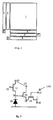
- FIG. 1 A general view of a CMOS image sensor is described in figure 1, wherein (1) represents one pixel array surrounded by dummy pixels, (2) represents row selection circuits, (3) represents buffers, (4) represents load transistors for the readout lines, (5) represents emitter follower transistors and multiplexers for the output voltages, (6) represents column selection circuits, (7) represents the output structure, (8 & 9) represent address input buffers.
- a row selection circuit selects one row of the array, putting the corresponding signals on vertical readout lines.
- the column selection circuit (6) selects one of the emitter followers, leading in that way the signal of one pixel to the output.
- each pixel contains one photodiode and 3 MOSFET transistors, and has a pitch of 6.6 micrometer using a 0.5 micrometer CMOS technology.
- the total number of transistors in the CMOS imaging sensor of the present embodiment amounts up to 808000.
- the fill factor can be only 15%.
- the small photosensitive area of this type of pixels (compared to the integrating type of imagers) does not degrade speed performance.
- the nominal supply voltage is 3.3 V, but it appears to work with no degradation between 1.7 V and 5 V.
- FIG 2 gives a schematic representation of the structure of a pixel (100) used in the device described in figure 1.
- Light is converted into a photodiode current (photodiode (10)) flowing through a load transistor (11).
- This current is in the order of femtoamperes to nanoamperes.
- the load transistor (11) operates in weak inversion, also called sub-threshold mode (V G ⁇ V th ) and as a consequence the photocurrent to voltage transition is logarithmic dependent on the current.
- the source voltage (12) of the load transistor (11) is buffered by an emitter follower (transistor 13).
- a selection transistor (14) of the pixel is connected to an activating line (15) and a data readout line (16).
- the sensitivity of the pixel disclosed in the state of the art at low light intensities may be limited by the leakage current through the load transistor (11).
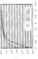
- curve a shows the logarithm of the current (Log(I)) trough the load transistor (11) as a function of voltage V.
- the gate length of transistors and more particularly of the load transistor (11) is increased by at least 10% compared to the gate length of transistors manufactured according to the layout rules of the CMOS manufacturing process.
- the gate length of the transistors such as the load transistor (11) is usually dictated by the requirements of the minimum area occupation and is imposed by the layout rules used for a specific CMOS manufacturing process advised by the silicon foundry.
- Such CMOS manufacturing process can be a 0.7 ⁇ m, 0.6 ⁇ m, 0.5 ⁇ m, 0.25 ⁇ m, 0.18 ⁇ m manufacturing process, or any other conventional manufacturing process known by the man skilled in the art.
- CMOS manufacturing process is defined by specific rules according to which devices such as CMOS image sensors can be fabricated.
- An important and more cited characteristic is also the characteristic defining the minimum dimension of the gate length of the transistors manufactured by such process.
- the transistors are designed with a gate length of 0.5 ⁇ m. This characteristic is therefore referred to in the sequel as the layout rules imposed by a specific CMOS manufacturing process.
- transistors such as transistors 13 & 14 of Figure 2
- transistors 13 & 14 of Figure 2 have a gate length of 0.5 ⁇ m, this means that they are fabricated by the 0.5 CMOS manufacturing process.
- At least the load transistor (11) should show a gate length of at least 0.55 ⁇ m.
- the load transistor (11) in figure 3 shows a saturation at lower current densities.
- Figure 3 is representing two examples of measurements done for two pixel structures as represented in figure 2, wherein the value [W x L] is [10 x 0.25 ⁇ m] and [10 x 0.5] ⁇ m respectively. Accordingly, in this figure wherein an increase of the gate length of 100% is represented, one can observe the sensitivity is increased by a factor of at least 4 decades.
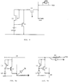
- FIG 4 is describing another preferred embodiment of a pixel structure according to the present invention which shows also a logarithmic response.
- This pixel has the main characteristics of the present invention and includes a photodiode (10), a load transistor (11) in series with the photodiode as well as read-out means (22 and 23).
- the drain of the load transistor (11) is not directly tied to the output signal supply.
- the read-out means consist in a second MOSFET (22) which is not a source follower and finally, a third MOSFET (23) which acts as a switch.
- a current source (24) is providing the current of the order of microamperes.
- the gate of the transistor (23) is tied to the address.
- the photodiode (10) can be considered as also a current source (of the order of femtoamperes to nanoamperes according to the intensity of light impinging the photodiode) the transistor (23) is conducting the current decharging through the transistor (22).
- Such current can be defined by: I 2 ⁇ c (V G - V th ) wherein c is a constant value.
- V G As I 2 is given by the current source and is more or less a constant, we have then V G also nearly a constant.
- the light acquired by the photodiode (10) is converted into a voltage drop across the load transistor (11).
- This pixel has accordingly the equivalent functions as the one described in figure 2.
- this pixel can be also considered as a simple and classic resistive feedback amplifier.
- Figure 5a and 5b describe a pixel structure for a CMOS sensor using only two MOSFETs (11 and 32) which can be read out in both X - Y (fig. 5a) and Y - X modes (fig. 5b). Since this array has X - Y interchangeability, one can choose to have addressing high speed in either X - or Y - directions which can be relevant for particular applications.
- one pixel comprises only a photodiode (50) and a switch (54) while the load transistor (51) and the read-out means (53) are common to one unit of pixels (500), a unit being e. g. a column or a row of pixels.
- an electronic circuit is provided by which an absolute measurement of the light intensity is realized.
- a pseudopixel (not represented) which does not have an imaging function is integrated in the imager as disclosed in figure 1.
- the photodiode (10) is replaced by current sources integrated in the chip according to techniques known by those skilled in the art.
- a known current density is generated by said current sources.
- the output voltage of said pseudopixel is compared to the output voltage of pixels containing a photodiode.
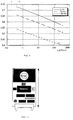
- an electronic circuit wherein certain error signals, known as so-called "white pixels” are corrected by an averaging or minimization operation on a group of pixels in the same area.
- An implementation is shown in figure 7.
- a group of 4 pixels (70) (71) (72) (73) is treated as one group for signal processing.
- a kind of minimum or average value or minimized value of the 4 pixels will be used for further processing.
- switches (74) and (75) will be closed and the output signal of pixel (70) will be replaced by an appropriate average value of the pixels (71) (72) and (73).
- FIG. 8 represents a sensor, according to the present invention, wherein the output voltage (80) of the pixel matrix (800) receives an offset correction before it is applied as an input voltage (82) to a signal processing unit, e.g. an Analog-to-Digital-Convertor (ADC) (83).
- ADC Analog-to-Digital-Convertor
- the output voltage (80) can be brought within the required range of input voltages of the ADC (83).
- a control circuit (84) with a lowpass filter transfer function (85) the output voltage (80) is increased or decreased until the input voltage (82) at the ADC (83) is within the selected range of the ADC (83).
- the correction on the output voltage (80) is given by a circuit (85) which yields a slowly varying voltage. This correction circuit acts as an automatic brightness regulating instance for the sensor (81).
- Non-uniformities in the read-out characteristics of the different pixels arise from the statistical spread on the threshold voltage (V th ) of the transistors (11-14) and photodiode (10) in the matrix.
- V th threshold voltage
- the actual non-uniformity is the sum of three V th distributions.
- the situation is especially unfavorable in the case when these transistors have submicron effective sizes which enhance the geometry dependant non-uniformity.
- the output signal must be offset corrected pixel by pixel, e.g. by using an external frame memory or by software.
- FIG. 9 illustrates that the stress operation can be performed without flattening the logarithmic response curve.
- the relaxation effect that occurs after the stress operation makes it necessary to stress the pixel in consecutive iterations. In this way the non-uniformity of the response is reduced to the level of the temporal noise ( ⁇ 5mV p/p).
- the pixel's threshold voltage will shift or degrade to a predetermined value.
- An imaging sensor as described hereabove can be used as an intelligent imager.
- imager can be achieved as an "imaging system on a chip" and is intended to be interfaced to the outside world without additional external circuiting or post processing.
- An addressable imager with logarithmic response behaves like a 256 Kbyte ROM : after applying an X - Y address (x - y position in matrix), the pixel intensity is returned.
- the following features are integrated:
- Such color mosaic filter preferably has the same structure as the pixel array structure of the CMOS image sensor.
- a mask set is used suited for the definition of the pixel structure of the CMOS image sensor and for preparing and depositing the color mosaic filter on the CMOS image sensor.
- the process of preparing this color mosaic filter comprises at least the following steps:
- the whole process may be repeated for depositing further colors.
- the dichromat may be used as photosensitive agent or alternatively photoresist pay be used.
- Figure 11 describes a preferred embodiment of a method of fabrication of such color filter comprising the following steps:
- the preceding steps may be repeated to deposit further colors.
Abstract
- a photosensitive element (10 or 50)
- a load transistor (11 or 51) in series with the photosensitive element (10 or 50);
- means comprising at least another transistor (13, 14 or 22, 23 or 32 or 53) coupled to said photosensitive element (10 or 50) and said load transistor (11 or 51) for reading out the signals acquired in said photosensitive element (10 or 50) and converting to a voltage drop across said load transistor (11 or 51), characterized in that the gate length of at least the load transistor (11 or 51) is increased by at least 10% compared to the gate length of the transistors manufactured according to the layout rules imposed by CMOS manufacturing process, whereby increasing the light sensitivity of said pixel structure.
Description
- The present invention relates to a pixel structure for imaging application, to CMOS image sensors using such pixel structure and to the corresponding peripheric circuitry.
- CCD-based cameras are commonly used as input devices for image analysis systems. A disadvantage of this class of devices is that when real-time operation is required, only essentially simple calculation can be performed on the CCD output data stream.
- Document US-A-5 335 008 is directed to a CCD image sensing device in which an amplifying transistor for amplifying a photoelectrically-converted signal charge and outputting the amplified signal charge to a vertical signal line is provided at every pixel of a plurality of pixels arrayed in a two-dimensional fashion and wherein a load transistor is connected to each of the vertical signal lines, in which the load transistor is composed of a first field effect transistor having a constant current characteristic and a second field effect transistor acting as a negative feedback resistor function connected in series.
- In this description, it is the first MOSFET transistor which is reacting as the load of a signal line and serving therefore as the load of a source follower. Accordingly, this transistor has no direct relation with the signal read from the photodiode.
- Furthermore, this document describes a CCD image sensing device wherein the first MOSFET transistor has a large ratio W/L wherein W is its channel width and L is its channel length.
- However, it should be noted that such W/L ratio affects directly the gate voltage (VG - Vth)) of the MOSFET for a given current. The aim of precising this characteristic is to suggest to have a linear resistance using MOSFET transistors. Accordingly to reach such linear operation it is necessary to work in the "VG > Vth" region.
- CMOS based flexible imaging sensors have been developed recently (S. Anderson, IEEE 1991, Custom Integrated Circuits Conference, pp. 12.1.1-12.1.4). Examples of these sensors include the IMPUTER of the company VLSI Vision Ltd. (Scotland) and the product MAP2200 of Integrated Vision Products (Sweden).
- Document EP-A-0 548 981 is describing a classic image sensor of the integrating type and having a particular source follower circuit. Each pixel in this image sensor comprises one MOSFET of a complex nature so that it includes light sensitive means. In this device, the photo current is accumulated on a capacitance and grows during elimination. At the end of "integration time", it must be reset. The same principle is found in many diode arrays, CCD's devices, MOSFET camera, etc.
- Document WO93/19489 describes an imaging chip intended to be use in a CMOS image sensor with a large number of image pixels are provided with field-effect transistors and a read-out logic. In order to map a high input signal dynamic ratio onto a reduced output signal dynamic ratio, each image pixel is connected to one electrode of a first MOS transistor and to the gate of a second MOS transistor while the other electrode of the first MOS transistor is connected to one pole of a voltage source.
- The reference Microelectronics Engineering 19 (1992) pp. 631-634 discloses an image array of 256 by 256 pixels developed in a 2.4 micron CMOS technology. Said array acts as an asynchronous component having as control signals of one pixel, two 8 bit input words forming the address of said pixel and one analog output. This device is fully addressable which implies that the pixels can be read out in a true random sequence. Furthermore, the pixels can be read out instantaneously, which is a consequence of the fact that in the chosen device architecture the detected photocurrent is continuously converted to a low impedance voltage signal within the pixel. A general view of the device architecture will be described in detail in the sequel and more particularly in connection with figures 1 and 2.
- The device described in such a document has a use as a compact, low cost smart vision sensor, e.g. for industrial imaging purposes. The device concept allows cointegration with digital logic, in order to build smart vision cameras. The logarithmic response causes this sensor to respond to a broad range of illumination conditions, with nearly perfect anti-blooming performance.
- The combination of the addressability and continuous, asynchronous readout characteristics allow to read out the response of any pixel any time. Both characteristics are intimately linked, adaptations in device architecture to improve one of both aspects have a direct advantageous leverage effect on the other (addressability or continuous read-out) characteristic.
- It is evident that using the above described technology, one can achieve a sensor having either addressability characteristics or continuous readout characteristics.
- The CMOS image sensor as disclosed in the above-mentioned reference shows apparent shortcomings for applications such as industrial imaging. The main disadvantage of the circuit as described in the prior art and currently on sale is that the quality of the image is inferior to the one of high-end CCD systems.
- More particularly, it is a first disadvantage of the circuit as described in the prior art and currently on sale is that the light sensitivity of the imaging device is limited by constraints inherently linked with the implementation in the CMOS technology.
- It is a second disadvantage of the circuit as described in the prior art and currently on sale is that an absolute measure of the light intensity cannot be provided due to the chosen device architecture.
- It is a third disadvantage of the circuit as described in the prior art and currently on sale is that a brightness control of the image cannot be achieved by state-of-the-art techniques applied for CCD's or for imaging devices based on integrating techniques.
- It is a fourth disadvantage that the homogeneity of the image is inherently degraded by the statistical spread on the individual pixel characteristics. Defective "white pixels" can degrade the image homogeneity as well.
- It is a fifth disadvantage that all the sensors described hereabove have only black and white contrast and accordingly, no color sensitivity.
- The aim of the present invention is to disclose new devices that overcome the drawbacks of the device and the circuit disclosed in the prior art.
- The present invention relates to a pixel structure for CMOS image sensors comprising a photosensitive element, a load transistor in series with the photosensitive element and means, comprising at least another transistor, coupled to said photosensitive element and said load transistor for reading out the signals acquired in said photosensitive element and converting it to a voltage drop across said load transistor. The present invention is essentially characterized by the fact that the gate length of at least the load transistor is increased by at least 10% compared to the gate length of transistors manufactured according to the layout rules imposed by the CMOS manufacturing process.
- According to one preferred embodiment, such structure can be realised in one individual pixel, and in such case, a CMOS image sensor will be achieved with a geometric configuration of a (j x k) matrix of pixels, each pixel having a photodiode, a load transistor and read-out means.
- According to one preferred embodiment, each pixel of the CMOS image sensor has at least one photodiode and a load transistor of which the drain is not tied to a voltage supplier and wherein the read-out means comprise at least a second transistor and a third transistor which is directly connected to the data read-out line.
- According to another preferred embodiment, each pixel of the CMOS image sensor has only one photodiode and two transistors among them a load transistor and another transistor connected to the data read-out line. Said pixel can be read-out in both X - Y and Y - X modes.
- According to another preferred embodiment, one pixel comprises only a photodiode and a switch since the load transistor and the read-out means are common for several pixels.
- Other characteristics and advantages are described hereunder.
-
- Figure 1:
- is a schematic view of the architecture of a CMOS image sensor according to the state of the art.
- Figure 2:
- is a schematic representation of the pixel structure as described in the state of the art and used in the sensor described in figure 1.
- Figure 3:
- is a measured graph representing the logarithmic value of the current through a MOSFET transistor (log(I)) versus the voltage (V), for different lengths of the MOSFET's gate for two precise embodiments of a pixel structure wherein the gate length is [10 µm x 0.25 µm] and [10 µm x 0.5 µm] respectively.
- Figures 4 & 5
- represent two other preferred embodiments of the new configuration for pixels structure for a CMOS sensor according to the present invention.
- Figure 6:
- represents another preferred embodiment of a configuration of pixels for a CMOS sensor according to the present invention.
- Figure 7:
- represents one implementation for a group of 2 x 2 pixels according to another preferred embodiment of the present invention.
- Figure 8:
- represents a schematic view of the peripheric circuit controlling the brightness for an image sensor according to the present invention.
- Figure 9:
- represents the responses of the light intensity (A) versus the sensor output voltage (V) for different stress conditions.
- Figure 10:
- represents a camera using the electronic image sensor according to the present invention.
- Figure 11:
- represents a flow sheet for the fabrication method of a color filter which will be laid on an image sensor according to the present invention.
- A general view of a CMOS image sensor is described in figure 1, wherein (1) represents one pixel array surrounded by dummy pixels, (2) represents row selection circuits, (3) represents buffers, (4) represents load transistors for the readout lines, (5) represents emitter follower transistors and multiplexers for the output voltages, (6) represents column selection circuits, (7) represents the output structure, (8 & 9) represent address input buffers. In operation, a row selection circuit selects one row of the array, putting the corresponding signals on vertical readout lines. The column selection circuit (6) selects one of the emitter followers, leading in that way the signal of one pixel to the output.
- In the following lines, for the purpose of the teaching of the invention, an implementation of the imaging sensor as a 512 x 512 active pixel CMOS imager is assumed. Each pixel contains one photodiode and 3 MOSFET transistors, and has a pitch of 6.6 micrometer using a 0.5 micrometer CMOS technology.
- The total number of transistors in the CMOS imaging sensor of the present embodiment amounts up to 808000. The fill factor can be only 15%. The small photosensitive area of this type of pixels (compared to the integrating type of imagers) does not degrade speed performance. The nominal supply voltage is 3.3 V, but it appears to work with no degradation between 1.7 V and 5 V.
- Figure 2 gives a schematic representation of the structure of a pixel (100) used in the device described in figure 1. Light is converted into a photodiode current (photodiode (10)) flowing through a load transistor (11). This current is in the order of femtoamperes to nanoamperes. Thus, the load transistor (11) operates in weak inversion, also called sub-threshold mode (VG << Vth) and as a consequence the photocurrent to voltage transition is logarithmic dependent on the current. The source voltage (12) of the load transistor (11) is buffered by an emitter follower (transistor 13). A selection transistor (14) of the pixel is connected to an activating line (15) and a data readout line (16).
- Thus, a fully addressable pixel matrix (1) with direct current sensing pixels (100) as described in figure 2 and having a logarithmic response is disclosed. in said reference.
- It is a first object of the present invention to provide a new pixel and a CMOS image sensor having improved light sensitivity. This means improved quality of the light/voltage conversion. The sensitivity of the pixel disclosed in the state of the art at low light intensities may be limited by the leakage current through the load transistor (11).
- In figure 3, curve a shows the logarithm of the current (Log(I)) trough the load transistor (11) as a function of voltage V. On this figure, one can see that at lower currents, the voltage over the transistor (11) is near zero and does not vary significantly.
- To overcome this limitation, the gate length of transistors and more particularly of the load transistor (11) is increased by at least 10% compared to the gate length of transistors manufactured according to the layout rules of the CMOS manufacturing process. The gate length of the transistors such as the load transistor (11) is usually dictated by the requirements of the minimum area occupation and is imposed by the layout rules used for a specific CMOS manufacturing process advised by the silicon foundry. Such CMOS manufacturing process can be a 0.7 µm, 0.6 µm, 0.5 µm, 0.25 µm, 0.18 µm manufacturing process, or any other conventional manufacturing process known by the man skilled in the art.
- A specific CMOS manufacturing process is defined by specific rules according to which devices such as CMOS image sensors can be fabricated.
- These rules comprise prescriptions for implementation of successive layers wherein thickness of oxides, diffusion time, and other characteristics known by the man skilled in the art are precisely followed.
- An important and more cited characteristic is also the characteristic defining the minimum dimension of the gate length of the transistors manufactured by such process.
- Therefore, for instance for a 0.5 µm CMOS manufacturing process, the transistors are designed with a gate length of 0.5 µm. This characteristic is therefore referred to in the sequel as the layout rules imposed by a specific CMOS manufacturing process.
- For instance if transistors (such as
transistors 13 & 14 of Figure 2) have a gate length of 0.5 µm, this means that they are fabricated by the 0.5 CMOS manufacturing process. - In this case, according to the present invention, at least the load transistor (11) should show a gate length of at least 0.55 µm.
- As a result of this characteristic, the load transistor (11) in figure 3 shows a saturation at lower current densities.
- An increased sensitivity of the pixel for lower light intensities (current densities) is apparent. The saturating regime in curve a is caused by the "punch through" phenomenon in the weak inversion region of MOS transistors. By increasing the gate length, a geometrical separation of source and drain regions is obtained, and the leakage current decreases. An increase of the sensitivity by a factor of 10 to 100 is realized.
- Figure 3 is representing two examples of measurements done for two pixel structures as represented in figure 2, wherein the value [W x L] is [10 x 0.25 µm] and [10 x 0.5] µm respectively. Accordingly, in this figure wherein an increase of the gate length of 100% is represented, one can observe the sensitivity is increased by a factor of at least 4 decades.
- Figure 4 is describing another preferred embodiment of a pixel structure according to the present invention which shows also a logarithmic response. This pixel has the main characteristics of the present invention and includes a photodiode (10), a load transistor (11) in series with the photodiode as well as read-out means (22 and 23).
- However, in this case, the drain of the load transistor (11) is not directly tied to the output signal supply. The read-out means consist in a second MOSFET (22) which is not a source follower and finally, a third MOSFET (23) which acts as a switch. A current source (24) is providing the current of the order of microamperes. The gate of the transistor (23) is tied to the address.
- While the photodiode (10) can be considered as also a current source (of the order of femtoamperes to nanoamperes according to the intensity of light impinging the photodiode) the transistor (23) is conducting the current decharging through the transistor (22). Such current can be defined by:

- As I2 is given by the current source and is more or less a constant, we have then VG also nearly a constant.
- Therefore, the light acquired by the photodiode (10) is converted into a voltage drop across the load transistor (11).
- This pixel has accordingly the equivalent functions as the one described in figure 2. Alternatively, this pixel can be also considered as a simple and classic resistive feedback amplifier.
- Figure 5a and 5b describe a pixel structure for a CMOS sensor using only two MOSFETs (11 and 32) which can be read out in both X - Y (fig. 5a) and Y - X modes (fig. 5b). Since this array has X - Y interchangeability, one can choose to have addressing high speed in either X - or Y - directions which can be relevant for particular applications.
- According to the X - Y mode described in fig. 5a, one can apply high voltage to the row to be addressed (36) while low voltage is applied to load column bus to ground (37).
- According to the Y - X mode represented in fig. 5b, one can apply low voltage to the column to be addressed (38) and high voltage to the load row bus to VDD supply (39).
- Using the same imaging area, one can increase the optical resolution using the pixel structure as described in figure 6.
- According to such configuration, one pixel comprises only a photodiode (50) and a switch (54) while the load transistor (51) and the read-out means (53) are common to one unit of pixels (500), a unit being e. g. a column or a row of pixels.
- It is a further object of the present invention that an electronic circuit is provided by which an absolute measurement of the light intensity is realized. Hereto, a pseudopixel (not represented) which does not have an imaging function is integrated in the imager as disclosed in figure 1. In said pseudopixel, the photodiode (10) is replaced by current sources integrated in the chip according to techniques known by those skilled in the art. A known current density is generated by said current sources. The output voltage of said pseudopixel is compared to the output voltage of pixels containing a photodiode. In order to determine the absolute light intensity on these pixels, which is proportional to the photocurrent and an independent calibration has still to be performed to determine the proportional coefficient between the light intensity and the photocurrent.
- It is a further object of the present invention that an electronic circuit is provided wherein certain error signals, known as so-called "white pixels" are corrected by an averaging or minimization operation on a group of pixels in the same area. An implementation is shown in figure 7. A group of 4 pixels (70) (71) (72) (73) is treated as one group for signal processing. According to the implementation shown, a kind of minimum or average value or minimized value of the 4 pixels will be used for further processing. In case one of the pixels, assume pixel (70), has a defective, e.g. leaking photodiode, in the addressing of the pixel, switches (74) and (75) will be closed and the output signal of pixel (70) will be replaced by an appropriate average value of the pixels (71) (72) and (73). It is evident that any other implementation of such correction method can be imagined. Any (m x n) group of pixels within the pixel matrix will lead to the same result if some kind of averaging or minimization operation is performed and if the extreme values which arise from defective pixel(s) are disregarded.
- It is a further object of the invention that an electronic circuit is provided, with a built-in automatic control of the brightness of the image. Figure 8 represents a sensor, according to the present invention, wherein the output voltage (80) of the pixel matrix (800) receives an offset correction before it is applied as an input voltage (82) to a signal processing unit, e.g. an Analog-to-Digital-Convertor (ADC) (83). Hence, the output voltage (80) can be brought within the required range of input voltages of the ADC (83). By means of a control circuit (84) with a lowpass filter transfer function (85), the output voltage (80) is increased or decreased until the input voltage (82) at the ADC (83) is within the selected range of the ADC (83). The correction on the output voltage (80) is given by a circuit (85) which yields a slowly varying voltage. This correction circuit acts as an automatic brightness regulating instance for the sensor (81).
- It is a further object of the present invention that an electronic circuit is provided in which on chip a non-uniformity correction is realized. Non-uniformities in the read-out characteristics of the different pixels arise from the statistical spread on the threshold voltage (Vth) of the transistors (11-14) and photodiode (10) in the matrix. For each pixel, the actual non-uniformity is the sum of three Vth distributions. The situation is especially unfavorable in the case when these transistors have submicron effective sizes which enhance the geometry dependant non-uniformity. For an acceptable image quality, the output signal must be offset corrected pixel by pixel, e.g. by using an external frame memory or by software. This jeopardizes the possibility of self-contained single chip smart vision camera. The solution to this problem was found to correct the offset internally in the pixel itself without increasing the size of the pixel or sensor, and without needing any external memory or software overhead. The hot carrier degradation of MOS transistors which is normally considered as a detrimental effect in semiconductor devices is advantageously used. Degradation experiments indicate that to first approach only threshold voltages are affected while the other transistor parameters such as the transconductance remain quite stable. This characteristic is used as a method to realize a homogeneous response for all the pixels as represented in figure 2. A high current density is loaded on e. g. the source follower transistor (13) or any other by applying strongly different voltages (17) and (16) and an appropriate voltage on (12). Taking programming voltages of 16V at (17), 9V for (12), 6V for (15) and 0V for (16), voltage shifts of 200 mV are realised in about 10 minutes. Figure 9 illustrates that the stress operation can be performed without flattening the logarithmic response curve. The relaxation effect that occurs after the stress operation makes it necessary to stress the pixel in consecutive iterations. In this way the non-uniformity of the response is reduced to the level of the temporal noise (<5mV p/p). As a result the pixel's threshold voltage will shift or degrade to a predetermined value. By repeating the operation for different pixels on different times, a pixel matrix with uniform response characteristics is obtained. One can also realize an analog non-volatile memory using this technique.
- An imaging sensor as described hereabove can be used as an intelligent imager. Such imager can be achieved as an "imaging system on a chip" and is intended to be interfaced to the outside world without additional external circuiting or post processing.
- For illustrating an application of this image sensor, its integration within a camera module, the "Fuga 15a" smart camera, is disclosed in figure 10.
- An addressable imager with logarithmic response behaves like a 256 Kbyte ROM : after applying an X - Y address (x - y position in matrix), the pixel intensity is returned. The following features are integrated:
- total die size: 3.6 x 3.6 mm2,
- 512 x 512 3-transistor pixels, pitch 6.6 µm,
- layer of dummy pixels around the active matrix,
- pixels have a continuous operation in time (non-integrating),
- logarithmic intensity to voltage conversion,
- extra column with reference current sources for calibration of the pixel photocurrents,
- output load 20 pF,
- addressing
speed 4 Mhz (X), up to 500 kHz (Y), - supply 3.0..3.3 V (operates also from 1.7 to 5 V - but behavior and lifetime not documented).
- It is another object of the present invention to provide a CMOS image sensor having a color sensitivity. Therefore, a color mosaic filter is prepared and deposited on the pixel structure of the CMOS image sensor according to the present invention.
- Such color mosaic filter preferably has the same structure as the pixel array structure of the CMOS image sensor. In order to achieve this structure, a mask set is used suited for the definition of the pixel structure of the CMOS image sensor and for preparing and depositing the color mosaic filter on the CMOS image sensor.
- The process of preparing this color mosaic filter comprises at least the following steps:
- preparation of a color mixture in the form of a suspension, dispersion or solution containing at least polyvinyl alcohol, dichromat and the required pigment or dye
- spinning this color preparation on the pixel structure of the CMOS image sensor
- illuminating using a mask set suited for the pixel structure of the CMOS image sensor
- etching the illuminated part including rinsing and/or flashing steps.
- The whole process may be repeated for depositing further colors.
- In the above described embodiment the dichromat may be used as photosensitive agent or alternatively photoresist pay be used.
- A preferred embodiment according to the above described process is as follows :
- preparation of the color mixture comprising 10 ml dye and 1 ml dichromat (0.35 g dichromat in 10 ml H2O)
- spinning at 3000 rpm up to a thickness of 1.0 - 1.5 µm
- illuminating for a time period of 50 sec
- etching by rinsing with desionized water
- 30 sec oxygen plasma flashing (150 Watt).
- Figure 11 describes a preferred embodiment of a method of fabrication of such color filter comprising the following steps:
-
- 1st color mixture (blue) obtained as described hereabove
- spinning at 4000 t/min (step a)
- illumination without any mask during 50 sec
-
- spinning at 2500 t/min (step b)
- baking at 130°C for 20 hrs
-
- spinning at 4300 t/min (step c)
- pre-baked at 100°C for 15 min
- illumination with mask - 18 sec
- developing 351 - 1'10'' (step d)
- full-baking at 110°C for 15 min
-
- CF4: 100 sccm
- Ar: 10 sccm
- 150 Watt - 240 sec (step e)
-
- O2: 10 sccm
- 150 Watt - 10 min (step f)
- The preceding steps may be repeated to deposit further colors.
Claims (13)
- A pixel (100 or 500) structure for CMOS imaging applications, comprising:- a photosensitive element (10 or 50)- a load transistor (11 or 51) in series with the photosensitive element (10 or 50);- means comprising at least another transistor (13, 14 or 22, 23 or 32 or 53) coupled to said photosensitive element (10 or 50) and said load transistor (11 or 51) for reading out the signals acquired in said photosensitive element (10 or 50) and converting to a voltage drop across said load transistor (11 or 51), characterized in that the gate length of at least the load transistor (11 or 51) is increased by at least 10% compared to the gate length of the transistors manufactured according to the layout rules imposed by CMOS manufacturing process, whereby increasing the light sensitivity of said pixel structure.
- A CMOS image sensor having a geometric configuration of pixels (100) consisting in a structure as claimed in claim 1, each pixel having at least one photodiode (10) and a load transistor (11) having its gate tied to a voltage (12) and wherein the read-out means comprise at least a second transistor which is an emitter follower (13) connected to a data read-out line (16).
- A CMOS image sensor having a geometric configuration of pixel (100) consisting in a structure as claimed in claim 1, each pixel having at least one photodiode (10) and a load transistor (11) of which the drain is not tied to a voltage and wherein the read-out means comprise a second transistor (22) and a third transistor (23) which is acting as a switch and is connected to a data read-out line (26).
- A CMOS image sensor having a geometric configuration of pixel (100) consisting in a structure as claimed in claim 1, each pixel having at least one photodiode (10) and a load transistor (11) and read-out means comprising only another transistor (32), said pixel being read-out in both X - Y, and Y - X modes.
- A CMOS image sensor having a geometric configuration of pixels (500) comprising a structure as claimed in claim 1 characterized in that each pixel (500) includes only a photodiode (50) and a switch (52), the load transistor (51) and the readout means (53) being common for one unit of several individual pixels (500).
- A CMOS image sensor as claimed in any one of the claims 2 to 5 characterized in that it further comprises at least one pseudopixel comprising a current source instead of a photodiode, in order to determine the absolute light intensity of the pixels.
- A CMOS image sensor as claimed in anyone of the claims 2 to 6 characterized in that it further comprises defined groups of (n x m) pixels (70, 71, 72 ,73) yielding one output voltage signal, said output voltage signal being some kind of average or minimized value of the individual output voltage signals of non-defective pixels in one group.
- A CMOS image sensor as claimed in any one of the claims 2 to 7 characterized in that it further comprises a mosaic color filter which has preferably the structure of the pixel array.
- Device comprising an image sensor as claimed in anyone of the claims 2 to 8 with a corresponding peripheric circuitry characterized in that it comprises- a signal processing unit (83),- a control circuit (84, 85) to adjust the output voltage signal (80) of the pixels (100) or units of pixel (500) in the sensor (800) within the input voltage (82) range of said signal processing unit (83),thereby providing an automatic brightness control of said sensor.
- Method for increasing the homogeneity of the image found in an image sensor as claimed in anyone of the claims 2 to 6 characterized in that it comprises the following steps:- selecting an individual pixel (100 or 500),- loading a high current density on one of the transistors (11, 13, 14 or 53) of one pixel for a time span, said time span being chosen to shift the threshold voltage of said transistor (11, 13, 14 or 53) to a predetermined value.
- Method for the fabrication of a color filter to be deposited on a CMOS image sensor according to claim 8 comprising the following steps:- preparation of a color mixture in the form of a suspension, dispersion or solution containing at least polyvinyl alcohol, dichromat and the required pigment or dye- spinning this color preparation on the pixel structure of the CMOS image sensor- illuminating using preferably the same mask set as the one used for manufacturing the pixel structure of the CMOS image sensor- etching the illuminated part including rinsing and/or flashing steps
- Method according to claim 11 wherein the processing steps as recited therein are repeated for further colors.
- Use of anyone of the devices claimed in any one of the claims 1 to 9 or of the methods claimed in claim 10, 11, and 12 for manufacturing a vision camera.
Priority Applications (2)
| Application Number | Priority Date | Filing Date | Title |
|---|---|---|---|
| US08/635,035 US5933190A (en) | 1995-04-18 | 1996-04-18 | Pixel structure, image sensor using such pixel structure and corresponding peripheral circuitry |
| EP96870050A EP0739039A3 (en) | 1995-04-18 | 1996-04-18 | Pixel structure, image sensor using such pixel, structure and corresponding peripheric circuitry |
Applications Claiming Priority (6)
| Application Number | Priority Date | Filing Date | Title |
|---|---|---|---|
| EP95870037 | 1995-04-18 | ||
| EP95870037 | 1995-04-18 | ||
| EP95870053 | 1995-05-12 | ||
| EP95870053 | 1995-05-12 | ||
| US08/635,035 US5933190A (en) | 1995-04-18 | 1996-04-18 | Pixel structure, image sensor using such pixel structure and corresponding peripheral circuitry |
| EP96870050A EP0739039A3 (en) | 1995-04-18 | 1996-04-18 | Pixel structure, image sensor using such pixel, structure and corresponding peripheric circuitry |
Publications (2)
| Publication Number | Publication Date |
|---|---|
| EP0739039A2 true EP0739039A2 (en) | 1996-10-23 |
| EP0739039A3 EP0739039A3 (en) | 1998-03-04 |
Family
ID=27443146
Family Applications (1)
| Application Number | Title | Priority Date | Filing Date |
|---|---|---|---|
| EP96870050A Withdrawn EP0739039A3 (en) | 1995-04-18 | 1996-04-18 | Pixel structure, image sensor using such pixel, structure and corresponding peripheric circuitry |
Country Status (2)
| Country | Link |
|---|---|
| US (1) | US5933190A (en) |
| EP (1) | EP0739039A3 (en) |
Cited By (23)
| Publication number | Priority date | Publication date | Assignee | Title |
|---|---|---|---|---|
| EP0856958A2 (en) * | 1997-01-30 | 1998-08-05 | AT&T Corp. | Method and apparatus for tracking alignment in wireless optical communication |
| EP0858111A1 (en) * | 1997-02-10 | 1998-08-12 | Interuniversitair Micro-Elektronica Centrum Vzw | A detector for electromagnetic radiation, pixel structure with high sensitivity using such detector and method of manufacturing such detector |
| EP0883187A1 (en) * | 1997-06-04 | 1998-12-09 | Interuniversitair Micro-Elektronica Centrum Vzw | A detector for electromagnetic radiation, pixel structure with high sensitivity using such detector and method of manufacturing such detector |
| WO1999009738A1 (en) * | 1997-08-20 | 1999-02-25 | Signalbau Huber Ag | Camera assembly for exposures and method for image evaluation |
| US6011251A (en) * | 1997-06-04 | 2000-01-04 | Imec | Method for obtaining a high dynamic range read-out signal of a CMOS-based pixel structure and such CMOS-based pixel structure |
| US6243134B1 (en) * | 1998-02-27 | 2001-06-05 | Intel Corporation | Method to reduce reset noise in photodiode based CMOS image sensors |
| WO2001061990A1 (en) * | 2000-02-19 | 2001-08-23 | Robert Bosch Gmbh | Video sensor chip circuit |
| EP1187217A2 (en) * | 2000-08-31 | 2002-03-13 | Minolta Co., Ltd. | Solid-state image sensing device |
| EP0858212B1 (en) * | 1997-02-10 | 2002-05-29 | Fill Factory | Method for obtaining a high dynamic range read-out signal of a CMOS-based pixel structure and such CMOS-based pixel structure |
| US6815791B1 (en) | 1997-02-10 | 2004-11-09 | Fillfactory | Buried, fully depletable, high fill factor photodiodes |
| US6917029B2 (en) | 1997-02-10 | 2005-07-12 | Fillfactory | Four-component pixel structure leading to improved image quality |
| US7030434B1 (en) | 1999-09-30 | 2006-04-18 | Infineon Technologies Ag | Arrangement with image sensors |
| DE10123819B4 (en) * | 2000-06-06 | 2006-07-27 | Sharp K.K. | Solid state image sensor and device with such |
| US7106373B1 (en) | 1998-02-09 | 2006-09-12 | Cypress Semiconductor Corporation (Belgium) Bvba | Method for increasing dynamic range of a pixel by multiple incomplete reset |
| US7199410B2 (en) | 1999-12-14 | 2007-04-03 | Cypress Semiconductor Corporation (Belgium) Bvba | Pixel structure with improved charge transfer |
| US7313288B2 (en) | 2005-04-20 | 2007-12-25 | Cypress Semiconductor Corporation | Defect pixel correction in an image sensor |
| EP1919193A2 (en) * | 2006-11-02 | 2008-05-07 | Omron Corporation | Imaging device, and control method for solid imaging element |
| EP2025005A2 (en) * | 2006-05-19 | 2009-02-18 | The Trustees of the University of Pennsylvania | A cmos linear voltage/current dual-mode imager |
| US7750958B1 (en) | 2005-03-28 | 2010-07-06 | Cypress Semiconductor Corporation | Pixel structure |
| US7808022B1 (en) | 2005-03-28 | 2010-10-05 | Cypress Semiconductor Corporation | Cross talk reduction |
| US8063963B2 (en) | 1998-02-09 | 2011-11-22 | On Semiconductor Image Sensor | Imaging device having a pixel structure with high dynamic range read-out signal |
| US8476567B2 (en) | 2008-09-22 | 2013-07-02 | Semiconductor Components Industries, Llc | Active pixel with precharging circuit |
| DE10251735B4 (en) * | 2001-11-06 | 2014-07-31 | Semiconductor Components Industries, Llc | Active pixel and method of making an active pixel |
Families Citing this family (95)
| Publication number | Priority date | Publication date | Assignee | Title |
|---|---|---|---|---|
| JP3359258B2 (en) | 1997-05-30 | 2002-12-24 | キヤノン株式会社 | Photoelectric conversion device, image sensor and image reading device using the same |
| US6130713A (en) * | 1997-06-27 | 2000-10-10 | Foveonics, Inc. | CMOS active pixel cell with self reset for improved dynamic range |
| DE19743580B4 (en) * | 1997-10-02 | 2004-12-02 | Robert Bosch Gmbh | Method and arrangement for determining the lighting conditions in the front of a moving vehicle, in particular in front of a motor vehicle |
| JP3466886B2 (en) * | 1997-10-06 | 2003-11-17 | キヤノン株式会社 | Solid-state imaging device |
| US6504572B2 (en) * | 1997-11-05 | 2003-01-07 | Stmicroelectronics, Inc. | Circuit for detecting leaky access switches in CMOS imager pixels |
| US6836291B1 (en) * | 1998-04-30 | 2004-12-28 | Minolta Co., Ltd. | Image pickup device with integral amplification |
| US6734907B1 (en) | 1998-04-30 | 2004-05-11 | Minolta Co., Ltd. | Solid-state image pickup device with integration and amplification |
| KR100279295B1 (en) * | 1998-06-02 | 2001-02-01 | 윤종용 | Active pixel sensor |
| US6242728B1 (en) * | 1998-08-20 | 2001-06-05 | Foveon, Inc. | CMOS active pixel sensor using native transistors |
| US8479012B1 (en) * | 1999-10-19 | 2013-07-02 | Harris Technology, Llc | Using biometrics as an encryption key |
| US6339248B1 (en) * | 1999-11-15 | 2002-01-15 | Omnivision Technologies, Inc. | Optimized floating P+ region photodiode for a CMOS image sensor |
| US7030921B2 (en) | 2000-02-01 | 2006-04-18 | Minolta Co., Ltd. | Solid-state image-sensing device |
| JP2001218113A (en) * | 2000-02-02 | 2001-08-10 | Minolta Co Ltd | Solid-state image pickup device |
| US6355965B1 (en) * | 2000-03-29 | 2002-03-12 | Omnivision Technologies, Inc. | On-chip fixed pattern noise canceling logarithmic response imager sensor |
| US6873359B1 (en) | 2000-09-29 | 2005-03-29 | Rockwell Science Center, Llc. | Self-adjusting, adaptive, minimal noise input amplifier circuit |
| US6504141B1 (en) | 2000-09-29 | 2003-01-07 | Rockwell Science Center, Llc | Adaptive amplifier circuit with enhanced dynamic range |
| US6900839B1 (en) | 2000-09-29 | 2005-05-31 | Rockwell Science Center, Llc | High gain detector amplifier with enhanced dynamic range for single photon read-out of photodetectors |
| US6965707B1 (en) | 2000-09-29 | 2005-11-15 | Rockwell Science Center, Llc | Compact active pixel with low-noise snapshot image formation |
| JP2002204398A (en) * | 2000-10-05 | 2002-07-19 | Honda Motor Co Ltd | Image sensor |
| US6888572B1 (en) | 2000-10-26 | 2005-05-03 | Rockwell Science Center, Llc | Compact active pixel with low-noise image formation |
| US6538245B1 (en) | 2000-10-26 | 2003-03-25 | Rockwell Science Center, Llc. | Amplified CMOS transducer for single photon read-out of photodetectors |
| JP4485087B2 (en) * | 2001-03-01 | 2010-06-16 | 株式会社半導体エネルギー研究所 | Operation method of semiconductor device |
| WO2002073951A1 (en) * | 2001-03-09 | 2002-09-19 | Fastcom Technology Sa | Device for the extraction of freely-definable image segments from an image sensor |
| WO2003054922A2 (en) * | 2001-12-21 | 2003-07-03 | Koninklijke Philips Electronics N.V. | Image pick-up device and camera system comprising an image pick-up device |
| GB0224770D0 (en) * | 2002-10-24 | 2002-12-04 | Council Cent Lab Res Councils | Imaging device |
| US7215369B2 (en) * | 2003-04-02 | 2007-05-08 | Micron Technology, Inc. | Compact pixel reset circuits using reversed current readout |
| EP1620895B1 (en) * | 2003-05-08 | 2016-03-02 | The Science and Technology Facilities Council | Accelerated particle and high energy radiation sensor |
| US20040239782A1 (en) * | 2003-05-30 | 2004-12-02 | William Equitz | System and method for efficient improvement of image quality in cameras |
| US7547978B2 (en) | 2004-06-14 | 2009-06-16 | Micron Technology, Inc. | Underfill and encapsulation of semiconductor assemblies with materials having differing properties |
| US7235431B2 (en) * | 2004-09-02 | 2007-06-26 | Micron Technology, Inc. | Methods for packaging a plurality of semiconductor dice using a flowable dielectric material |
| US20070002153A1 (en) * | 2005-06-29 | 2007-01-04 | Bart Dierickx | Hue preservation |
| US7923298B2 (en) | 2007-09-07 | 2011-04-12 | Micron Technology, Inc. | Imager die package and methods of packaging an imager die on a temporary carrier |
| SE532553C2 (en) * | 2008-01-24 | 2010-02-23 | Mikael Lindstrand | Method and apparatus for obtaining high dynamic, spectral, spatial and angular resolved radius information |
| US8902321B2 (en) | 2008-05-20 | 2014-12-02 | Pelican Imaging Corporation | Capturing and processing of images using monolithic camera array with heterogeneous imagers |
| US11792538B2 (en) | 2008-05-20 | 2023-10-17 | Adeia Imaging Llc | Capturing and processing of images including occlusions focused on an image sensor by a lens stack array |
| US8866920B2 (en) | 2008-05-20 | 2014-10-21 | Pelican Imaging Corporation | Capturing and processing of images using monolithic camera array with heterogeneous imagers |
| US7974805B2 (en) * | 2008-10-14 | 2011-07-05 | ON Semiconductor Trading, Ltd | Image sensor and method |
| JP2011091487A (en) * | 2009-10-20 | 2011-05-06 | Panasonic Corp | Solid-state image pickup device |
| EP2502115A4 (en) | 2009-11-20 | 2013-11-06 | Pelican Imaging Corp | Capturing and processing of images using monolithic camera array with heterogeneous imagers |
| KR101824672B1 (en) | 2010-05-12 | 2018-02-05 | 포토네이션 케이맨 리미티드 | Architectures for imager arrays and array cameras |
| US8878950B2 (en) | 2010-12-14 | 2014-11-04 | Pelican Imaging Corporation | Systems and methods for synthesizing high resolution images using super-resolution processes |
| JP2014519741A (en) | 2011-05-11 | 2014-08-14 | ペリカン イメージング コーポレイション | System and method for transmitting and receiving array camera image data |
| US20130265459A1 (en) | 2011-06-28 | 2013-10-10 | Pelican Imaging Corporation | Optical arrangements for use with an array camera |
| EP2726930A4 (en) | 2011-06-28 | 2015-03-04 | Pelican Imaging Corp | Optical arrangements for use with an array camera |
| WO2013043761A1 (en) | 2011-09-19 | 2013-03-28 | Pelican Imaging Corporation | Determining depth from multiple views of a scene that include aliasing using hypothesized fusion |
| EP2761534B1 (en) | 2011-09-28 | 2020-11-18 | FotoNation Limited | Systems for encoding light field image files |
| WO2013119706A1 (en) * | 2012-02-06 | 2013-08-15 | Pelican Imaging Corporation | Systems and methods for extending dynamic range of imager arrays by controlling pixel analog gain |
| US9412206B2 (en) | 2012-02-21 | 2016-08-09 | Pelican Imaging Corporation | Systems and methods for the manipulation of captured light field image data |
| US9210392B2 (en) | 2012-05-01 | 2015-12-08 | Pelican Imaging Coporation | Camera modules patterned with pi filter groups |
| WO2014005123A1 (en) | 2012-06-28 | 2014-01-03 | Pelican Imaging Corporation | Systems and methods for detecting defective camera arrays, optic arrays, and sensors |
| US20140002674A1 (en) | 2012-06-30 | 2014-01-02 | Pelican Imaging Corporation | Systems and Methods for Manufacturing Camera Modules Using Active Alignment of Lens Stack Arrays and Sensors |
| CN107346061B (en) | 2012-08-21 | 2020-04-24 | 快图有限公司 | System and method for parallax detection and correction in images captured using an array camera |
| WO2014032020A2 (en) | 2012-08-23 | 2014-02-27 | Pelican Imaging Corporation | Feature based high resolution motion estimation from low resolution images captured using an array source |
| US9214013B2 (en) | 2012-09-14 | 2015-12-15 | Pelican Imaging Corporation | Systems and methods for correcting user identified artifacts in light field images |
| CN104685860A (en) | 2012-09-28 | 2015-06-03 | 派力肯影像公司 | Generating images from light fields utilizing virtual viewpoints |
| US9143711B2 (en) | 2012-11-13 | 2015-09-22 | Pelican Imaging Corporation | Systems and methods for array camera focal plane control |
| US9462164B2 (en) | 2013-02-21 | 2016-10-04 | Pelican Imaging Corporation | Systems and methods for generating compressed light field representation data using captured light fields, array geometry, and parallax information |
| US9253380B2 (en) | 2013-02-24 | 2016-02-02 | Pelican Imaging Corporation | Thin form factor computational array cameras and modular array cameras |
| US9638883B1 (en) | 2013-03-04 | 2017-05-02 | Fotonation Cayman Limited | Passive alignment of array camera modules constructed from lens stack arrays and sensors based upon alignment information obtained during manufacture of array camera modules using an active alignment process |
| US9774789B2 (en) | 2013-03-08 | 2017-09-26 | Fotonation Cayman Limited | Systems and methods for high dynamic range imaging using array cameras |
| US8866912B2 (en) | 2013-03-10 | 2014-10-21 | Pelican Imaging Corporation | System and methods for calibration of an array camera using a single captured image |
| US9521416B1 (en) | 2013-03-11 | 2016-12-13 | Kip Peli P1 Lp | Systems and methods for image data compression |
| WO2014165244A1 (en) | 2013-03-13 | 2014-10-09 | Pelican Imaging Corporation | Systems and methods for synthesizing images from image data captured by an array camera using restricted depth of field depth maps in which depth estimation precision varies |
| US9888194B2 (en) | 2013-03-13 | 2018-02-06 | Fotonation Cayman Limited | Array camera architecture implementing quantum film image sensors |
| US9106784B2 (en) | 2013-03-13 | 2015-08-11 | Pelican Imaging Corporation | Systems and methods for controlling aliasing in images captured by an array camera for use in super-resolution processing |
| WO2014164550A2 (en) | 2013-03-13 | 2014-10-09 | Pelican Imaging Corporation | System and methods for calibration of an array camera |
| US9578259B2 (en) | 2013-03-14 | 2017-02-21 | Fotonation Cayman Limited | Systems and methods for reducing motion blur in images or video in ultra low light with array cameras |
| WO2014153098A1 (en) | 2013-03-14 | 2014-09-25 | Pelican Imaging Corporation | Photmetric normalization in array cameras |
| US9497429B2 (en) | 2013-03-15 | 2016-11-15 | Pelican Imaging Corporation | Extended color processing on pelican array cameras |
| US10122993B2 (en) | 2013-03-15 | 2018-11-06 | Fotonation Limited | Autofocus system for a conventional camera that uses depth information from an array camera |
| WO2014145856A1 (en) | 2013-03-15 | 2014-09-18 | Pelican Imaging Corporation | Systems and methods for stereo imaging with camera arrays |
| US9445003B1 (en) | 2013-03-15 | 2016-09-13 | Pelican Imaging Corporation | Systems and methods for synthesizing high resolution images using image deconvolution based on motion and depth information |
| US9633442B2 (en) | 2013-03-15 | 2017-04-25 | Fotonation Cayman Limited | Array cameras including an array camera module augmented with a separate camera |
| US9497370B2 (en) | 2013-03-15 | 2016-11-15 | Pelican Imaging Corporation | Array camera architecture implementing quantum dot color filters |
| WO2015048694A2 (en) | 2013-09-27 | 2015-04-02 | Pelican Imaging Corporation | Systems and methods for depth-assisted perspective distortion correction |
| WO2015070105A1 (en) | 2013-11-07 | 2015-05-14 | Pelican Imaging Corporation | Methods of manufacturing array camera modules incorporating independently aligned lens stacks |
| US10119808B2 (en) | 2013-11-18 | 2018-11-06 | Fotonation Limited | Systems and methods for estimating depth from projected texture using camera arrays |
| EP3075140B1 (en) | 2013-11-26 | 2018-06-13 | FotoNation Cayman Limited | Array camera configurations incorporating multiple constituent array cameras |
| US10089740B2 (en) | 2014-03-07 | 2018-10-02 | Fotonation Limited | System and methods for depth regularization and semiautomatic interactive matting using RGB-D images |
| US9247117B2 (en) | 2014-04-07 | 2016-01-26 | Pelican Imaging Corporation | Systems and methods for correcting for warpage of a sensor array in an array camera module by introducing warpage into a focal plane of a lens stack array |
| US9521319B2 (en) | 2014-06-18 | 2016-12-13 | Pelican Imaging Corporation | Array cameras and array camera modules including spectral filters disposed outside of a constituent image sensor |
| CN113256730B (en) | 2014-09-29 | 2023-09-05 | 快图有限公司 | System and method for dynamic calibration of an array camera |
| US9942474B2 (en) | 2015-04-17 | 2018-04-10 | Fotonation Cayman Limited | Systems and methods for performing high speed video capture and depth estimation using array cameras |
| JP6727830B2 (en) * | 2016-02-09 | 2020-07-22 | キヤノン株式会社 | Imaging device |
| RU174758U1 (en) * | 2017-08-02 | 2017-10-31 | Общество с ограниченной ответственностью "Мультиспектр" | Photosensitive Sensor Matrix |
| US10482618B2 (en) | 2017-08-21 | 2019-11-19 | Fotonation Limited | Systems and methods for hybrid depth regularization |
| MX2022003020A (en) | 2019-09-17 | 2022-06-14 | Boston Polarimetrics Inc | Systems and methods for surface modeling using polarization cues. |
| EP4042366A4 (en) | 2019-10-07 | 2023-11-15 | Boston Polarimetrics, Inc. | Systems and methods for augmentation of sensor systems and imaging systems with polarization |
| KR20230116068A (en) | 2019-11-30 | 2023-08-03 | 보스턴 폴라리메트릭스, 인크. | System and method for segmenting transparent objects using polarization signals |
| CN115552486A (en) | 2020-01-29 | 2022-12-30 | 因思创新有限责任公司 | System and method for characterizing an object pose detection and measurement system |
| KR20220133973A (en) | 2020-01-30 | 2022-10-05 | 인트린식 이노베이션 엘엘씨 | Systems and methods for synthesizing data to train statistical models for different imaging modalities, including polarized images |
| WO2021243088A1 (en) | 2020-05-27 | 2021-12-02 | Boston Polarimetrics, Inc. | Multi-aperture polarization optical systems using beam splitters |
| US11954886B2 (en) | 2021-04-15 | 2024-04-09 | Intrinsic Innovation Llc | Systems and methods for six-degree of freedom pose estimation of deformable objects |
| US11290658B1 (en) | 2021-04-15 | 2022-03-29 | Boston Polarimetrics, Inc. | Systems and methods for camera exposure control |
| US11689813B2 (en) | 2021-07-01 | 2023-06-27 | Intrinsic Innovation Llc | Systems and methods for high dynamic range imaging using crossed polarizers |
Citations (4)
| Publication number | Priority date | Publication date | Assignee | Title |
|---|---|---|---|---|
| US4565756A (en) * | 1981-11-10 | 1986-01-21 | U.S. Philips Corporation | Color imaging device |
| EP0548987A2 (en) * | 1991-12-26 | 1993-06-30 | Sony Corporation | Source follower circuit for image sensor |
| WO1993019489A1 (en) * | 1992-03-24 | 1993-09-30 | Institut Für Mikroelektronik Stuttgart | Image cell, in particular for an imaging chip |
| US5335008A (en) * | 1991-03-08 | 1994-08-02 | Sony Corporation | Imager which has a load transistor connected to each vertical signal line and wherein each load transistor comprises two field transistors connected in series |
Family Cites Families (9)
| Publication number | Priority date | Publication date | Assignee | Title |
|---|---|---|---|---|
| US5144447A (en) * | 1988-03-31 | 1992-09-01 | Hitachi, Ltd. | Solid-state image array with simultaneously activated line drivers |
| US5122881A (en) * | 1988-08-10 | 1992-06-16 | Hitachi, Ltd. | Solid-state imaging device with an amplifying FET in each pixel and an output capacitor in each row |
| DE69226111T2 (en) * | 1991-03-16 | 1998-12-24 | Toshiba Kawasaki Kk | Color imaging method with integration time control |
| JP2575964B2 (en) * | 1991-03-27 | 1997-01-29 | 株式会社東芝 | Solid-state imaging device |
| US5502488A (en) * | 1991-05-07 | 1996-03-26 | Olympus Optical Co., Ltd. | Solid-state imaging device having a low impedance structure |
| JP2965777B2 (en) * | 1992-01-29 | 1999-10-18 | オリンパス光学工業株式会社 | Solid-state imaging device |
| US5453783A (en) * | 1992-09-02 | 1995-09-26 | Martin Marietta Corporation | General absolute value circuit |
| US5336879A (en) * | 1993-05-28 | 1994-08-09 | David Sarnoff Research Center, Inc. | Pixel array having image forming pixel elements integral with peripheral circuit elements |
| US5488415A (en) * | 1993-07-09 | 1996-01-30 | Olympus Optical Co., Ltd. | Solid-state image pickup device having a photoelectric conversion detection cell with high sensitivity |
-
1996
- 1996-04-18 US US08/635,035 patent/US5933190A/en not_active Expired - Lifetime
- 1996-04-18 EP EP96870050A patent/EP0739039A3/en not_active Withdrawn
Patent Citations (4)
| Publication number | Priority date | Publication date | Assignee | Title |
|---|---|---|---|---|
| US4565756A (en) * | 1981-11-10 | 1986-01-21 | U.S. Philips Corporation | Color imaging device |
| US5335008A (en) * | 1991-03-08 | 1994-08-02 | Sony Corporation | Imager which has a load transistor connected to each vertical signal line and wherein each load transistor comprises two field transistors connected in series |
| EP0548987A2 (en) * | 1991-12-26 | 1993-06-30 | Sony Corporation | Source follower circuit for image sensor |
| WO1993019489A1 (en) * | 1992-03-24 | 1993-09-30 | Institut Für Mikroelektronik Stuttgart | Image cell, in particular for an imaging chip |
Non-Patent Citations (2)
| Title |
|---|
| N. RICQUIER ET AL.: "PIXEL STRUCTURE WITH LOGARITHMIC RESPONSE FOR INTELLIGENT AND FLEXIBLE IMAGER ARCHITECTURES" MICRO ELECTRONIC ENGINEERING, vol. 19, no. 1-4, 14 September 1992, LEUVEN, BELGIUM, pages 631-634, XP000357124 * |
| S ANDERSON ET AL.: "A SINGLE CHIP SENSOR & IMAGE PROCESSOR FOR FINGERPRINT VERIFICATION" IEEE 1991 CUSTOM INTEGRATED CIRCUITS CONFERENCE, 12 May 1991, SAN DIEGO, CALIFORNIA, pages 12.1.1-12.1.4, XP000295730 * |
Cited By (31)
| Publication number | Priority date | Publication date | Assignee | Title |
|---|---|---|---|---|
| EP0856958A3 (en) * | 1997-01-30 | 1999-09-01 | AT&T Corp. | Method and apparatus for tracking alignment in wireless optical communication |
| EP0856958A2 (en) * | 1997-01-30 | 1998-08-05 | AT&T Corp. | Method and apparatus for tracking alignment in wireless optical communication |
| US6815791B1 (en) | 1997-02-10 | 2004-11-09 | Fillfactory | Buried, fully depletable, high fill factor photodiodes |
| KR100545801B1 (en) * | 1997-02-10 | 2006-04-21 | 필 팩토리 | Electromagnetic radiation detectors, high sensitivity pixel structures using such detectors and methods of manufacturing such detectors. |
| EP0858111A1 (en) * | 1997-02-10 | 1998-08-12 | Interuniversitair Micro-Elektronica Centrum Vzw | A detector for electromagnetic radiation, pixel structure with high sensitivity using such detector and method of manufacturing such detector |
| US6917029B2 (en) | 1997-02-10 | 2005-07-12 | Fillfactory | Four-component pixel structure leading to improved image quality |
| US7253019B2 (en) | 1997-02-10 | 2007-08-07 | Cypress Semiconductor Corporation (Belgium) Bvba | Buried, fully depletable, high fill factor photodiodes |
| EP0858212B1 (en) * | 1997-02-10 | 2002-05-29 | Fill Factory | Method for obtaining a high dynamic range read-out signal of a CMOS-based pixel structure and such CMOS-based pixel structure |
| EP0883187A1 (en) * | 1997-06-04 | 1998-12-09 | Interuniversitair Micro-Elektronica Centrum Vzw | A detector for electromagnetic radiation, pixel structure with high sensitivity using such detector and method of manufacturing such detector |
| US6011251A (en) * | 1997-06-04 | 2000-01-04 | Imec | Method for obtaining a high dynamic range read-out signal of a CMOS-based pixel structure and such CMOS-based pixel structure |
| US6225670B1 (en) | 1997-06-04 | 2001-05-01 | Imec | Detector for electromagnetic radiation, pixel structure with high sensitivity using such detector and method of manufacturing such detector |
| WO1999009738A1 (en) * | 1997-08-20 | 1999-02-25 | Signalbau Huber Ag | Camera assembly for exposures and method for image evaluation |
| US7106373B1 (en) | 1998-02-09 | 2006-09-12 | Cypress Semiconductor Corporation (Belgium) Bvba | Method for increasing dynamic range of a pixel by multiple incomplete reset |
| US8063963B2 (en) | 1998-02-09 | 2011-11-22 | On Semiconductor Image Sensor | Imaging device having a pixel structure with high dynamic range read-out signal |
| US6317154B2 (en) | 1998-02-27 | 2001-11-13 | Intel Corporation | Method to reduce reset noise in photodiode based CMOS image sensors |
| US6243134B1 (en) * | 1998-02-27 | 2001-06-05 | Intel Corporation | Method to reduce reset noise in photodiode based CMOS image sensors |
| US7030434B1 (en) | 1999-09-30 | 2006-04-18 | Infineon Technologies Ag | Arrangement with image sensors |
| US7199410B2 (en) | 1999-12-14 | 2007-04-03 | Cypress Semiconductor Corporation (Belgium) Bvba | Pixel structure with improved charge transfer |
| WO2001061990A1 (en) * | 2000-02-19 | 2001-08-23 | Robert Bosch Gmbh | Video sensor chip circuit |
| DE10123819B4 (en) * | 2000-06-06 | 2006-07-27 | Sharp K.K. | Solid state image sensor and device with such |
| EP1187217A2 (en) * | 2000-08-31 | 2002-03-13 | Minolta Co., Ltd. | Solid-state image sensing device |
| DE10251735B4 (en) * | 2001-11-06 | 2014-07-31 | Semiconductor Components Industries, Llc | Active pixel and method of making an active pixel |
| US7808022B1 (en) | 2005-03-28 | 2010-10-05 | Cypress Semiconductor Corporation | Cross talk reduction |
| US7750958B1 (en) | 2005-03-28 | 2010-07-06 | Cypress Semiconductor Corporation | Pixel structure |
| US7313288B2 (en) | 2005-04-20 | 2007-12-25 | Cypress Semiconductor Corporation | Defect pixel correction in an image sensor |
| EP2025005A2 (en) * | 2006-05-19 | 2009-02-18 | The Trustees of the University of Pennsylvania | A cmos linear voltage/current dual-mode imager |
| EP2025005A4 (en) * | 2006-05-19 | 2012-06-20 | Univ Pennsylvania | A cmos linear voltage/current dual-mode imager |
| EP1919193A3 (en) * | 2006-11-02 | 2011-10-05 | OMRON Automotive Electronics Co., Ltd. | Imaging device, and control method for solid imaging element |
| US8045030B2 (en) | 2006-11-02 | 2011-10-25 | Omron Automotive Electronics Co., Ltd. | Imaging device, and control method for solid imaging element |
| EP1919193A2 (en) * | 2006-11-02 | 2008-05-07 | Omron Corporation | Imaging device, and control method for solid imaging element |
| US8476567B2 (en) | 2008-09-22 | 2013-07-02 | Semiconductor Components Industries, Llc | Active pixel with precharging circuit |
Also Published As
| Publication number | Publication date |
|---|---|
| EP0739039A3 (en) | 1998-03-04 |
| US5933190A (en) | 1999-08-03 |
Similar Documents
| Publication | Publication Date | Title |
|---|---|---|
| EP0739039A2 (en) | Pixel structure, image sensor using such pixel, structure and corresponding peripheric circuitry | |
| US5920345A (en) | CMOS image sensor with improved fill factor | |
| KR100572206B1 (en) | DC offset and gain correction method and system for CMOS image sensor | |
| US5881184A (en) | Active pixel sensor with single pixel reset | |
| US6476864B1 (en) | Pixel sensor column amplifier architecture | |
| US6320616B1 (en) | CMOS image sensor with reduced fixed pattern noise | |
| US6943838B2 (en) | Active pixel sensor pixel having a photodetector whose output is coupled to an output transistor gate | |
| Scheffer et al. | Random addressable 2048/spl times/2048 active pixel image sensor | |
| US6704050B1 (en) | Active-pixel image sensing device with linear mode voltage to current conversion | |
| CN102037722B (en) | Solid-state imaging device, imaging device, and pixel driving method | |
| Jansson et al. | An addressable 256× 256 photodiode image sensor array with an 8-bit digital output | |
| EP1187217A2 (en) | Solid-state image sensing device | |
| JP2000502224A (en) | Imaging system | |
| US20050117042A1 (en) | Semiconductor image pickup device capable of sensing light over wider range | |
| US7271432B2 (en) | Image-sensing apparatus | |
| Ricquier et al. | Pixel structure with logarithmic response for intelligent and flexible imager architectures | |
| US6917029B2 (en) | Four-component pixel structure leading to improved image quality | |
| EP1117250A2 (en) | Active pixel sensor with improved reference signal | |
| US7098951B2 (en) | Image pickup device with high contrast detection capability | |
| US6747700B1 (en) | Solid state image pickup apparatus having a plurality of split buses | |
| US7236192B2 (en) | Image-sensing device | |
| JPH09298286A (en) | Pixel structure, image sensor using the pixel structure and adaptable peripheral circuit mechanism | |
| KR19980080491A (en) | Active pixel image sensing device and manufacturing method thereof | |
| JPH05190827A (en) | Solid-stase image-sensing device | |
| JPH03118425A (en) | Photometric sensor |
Legal Events
| Date | Code | Title | Description |
|---|---|---|---|
| PUAI | Public reference made under article 153(3) epc to a published international application that has entered the european phase |
Free format text: ORIGINAL CODE: 0009012 |
|
| 17P | Request for examination filed |
Effective date: 19960508 |
|
| AK | Designated contracting states |
Kind code of ref document: A2 Designated state(s): AT BE CH DE DK ES FI FR GB IE IT LI NL SE |
|
| DET | De: translation of patent claims | ||
| PUAL | Search report despatched |
Free format text: ORIGINAL CODE: 0009013 |
|
| AK | Designated contracting states |
Kind code of ref document: A3 Designated state(s): AT BE CH DE DK ES FI FR GB IE IT LI NL SE |
|
| RAP1 | Party data changed (applicant data changed or rights of an application transferred) |
Owner name: FILL FACTORY |
|
| 17Q | First examination report despatched |
Effective date: 20030410 |
|
| STAA | Information on the status of an ep patent application or granted ep patent |
Free format text: STATUS: THE APPLICATION IS DEEMED TO BE WITHDRAWN |
|
| 18D | Application deemed to be withdrawn |
Effective date: 20030821 |