EP0735501A2 - Colour sensor arrangement for reading colour marks - Google Patents
Colour sensor arrangement for reading colour marks Download PDFInfo
- Publication number
- EP0735501A2 EP0735501A2 EP96103880A EP96103880A EP0735501A2 EP 0735501 A2 EP0735501 A2 EP 0735501A2 EP 96103880 A EP96103880 A EP 96103880A EP 96103880 A EP96103880 A EP 96103880A EP 0735501 A2 EP0735501 A2 EP 0735501A2
- Authority
- EP
- European Patent Office
- Prior art keywords
- sensor arrangement
- radiation
- semiconductor radiation
- color sensor
- receiving
- Prior art date
- Legal status (The legal status is an assumption and is not a legal conclusion. Google has not performed a legal analysis and makes no representation as to the accuracy of the status listed.)
- Granted
Links
- 230000003287 optical effect Effects 0.000 claims abstract description 28
- 230000005855 radiation Effects 0.000 claims description 62
- 239000004065 semiconductor Substances 0.000 claims description 40
- 230000005693 optoelectronics Effects 0.000 claims description 10
- 230000005540 biological transmission Effects 0.000 claims description 8
- 238000013461 design Methods 0.000 claims description 7
- 238000011156 evaluation Methods 0.000 claims description 5
- 230000003595 spectral effect Effects 0.000 claims description 3
- 230000000295 complement effect Effects 0.000 claims 1
- 239000002184 metal Substances 0.000 abstract description 3
- 239000007787 solid Substances 0.000 abstract 1
- 241000219739 Lens Species 0.000 description 36
- 238000013459 approach Methods 0.000 description 8
- 230000008901 benefit Effects 0.000 description 5
- 238000000576 coating method Methods 0.000 description 4
- 239000011248 coating agent Substances 0.000 description 3
- 239000003086 colorant Substances 0.000 description 3
- 239000011521 glass Substances 0.000 description 3
- 238000000034 method Methods 0.000 description 3
- 230000015572 biosynthetic process Effects 0.000 description 2
- 238000005755 formation reaction Methods 0.000 description 2
- 238000012544 monitoring process Methods 0.000 description 2
- 241001136792 Alle Species 0.000 description 1
- 240000004322 Lens culinaris Species 0.000 description 1
- 230000004308 accommodation Effects 0.000 description 1
- 230000006978 adaptation Effects 0.000 description 1
- 230000000903 blocking effect Effects 0.000 description 1
- 238000010276 construction Methods 0.000 description 1
- 238000011109 contamination Methods 0.000 description 1
- 238000010586 diagram Methods 0.000 description 1
- 238000006073 displacement reaction Methods 0.000 description 1
- 230000002349 favourable effect Effects 0.000 description 1
- 238000005286 illumination Methods 0.000 description 1
- 238000002347 injection Methods 0.000 description 1
- 239000007924 injection Substances 0.000 description 1
- 239000004922 lacquer Substances 0.000 description 1
- 238000012545 processing Methods 0.000 description 1
- 210000001747 pupil Anatomy 0.000 description 1
- 230000000717 retained effect Effects 0.000 description 1
- 229920006395 saturated elastomer Polymers 0.000 description 1
- 238000000926 separation method Methods 0.000 description 1
- 230000001629 suppression Effects 0.000 description 1
- 238000012549 training Methods 0.000 description 1
- 230000007704 transition Effects 0.000 description 1
- 238000007740 vapor deposition Methods 0.000 description 1
Images
Classifications
-
- G—PHYSICS
- G01—MEASURING; TESTING
- G01J—MEASUREMENT OF INTENSITY, VELOCITY, SPECTRAL CONTENT, POLARISATION, PHASE OR PULSE CHARACTERISTICS OF INFRARED, VISIBLE OR ULTRAVIOLET LIGHT; COLORIMETRY; RADIATION PYROMETRY
- G01J3/00—Spectrometry; Spectrophotometry; Monochromators; Measuring colours
- G01J3/46—Measurement of colour; Colour measuring devices, e.g. colorimeters
- G01J3/50—Measurement of colour; Colour measuring devices, e.g. colorimeters using electric radiation detectors
- G01J3/501—Colorimeters using spectrally-selective light sources, e.g. LEDs
-
- G—PHYSICS
- G01—MEASURING; TESTING
- G01J—MEASUREMENT OF INTENSITY, VELOCITY, SPECTRAL CONTENT, POLARISATION, PHASE OR PULSE CHARACTERISTICS OF INFRARED, VISIBLE OR ULTRAVIOLET LIGHT; COLORIMETRY; RADIATION PYROMETRY
- G01J3/00—Spectrometry; Spectrophotometry; Monochromators; Measuring colours
- G01J3/02—Details
- G01J3/0205—Optical elements not provided otherwise, e.g. optical manifolds, diffusers, windows
- G01J3/0208—Optical elements not provided otherwise, e.g. optical manifolds, diffusers, windows using focussing or collimating elements, e.g. lenses or mirrors; performing aberration correction
-
- G—PHYSICS
- G01—MEASURING; TESTING
- G01J—MEASUREMENT OF INTENSITY, VELOCITY, SPECTRAL CONTENT, POLARISATION, PHASE OR PULSE CHARACTERISTICS OF INFRARED, VISIBLE OR ULTRAVIOLET LIGHT; COLORIMETRY; RADIATION PYROMETRY
- G01J3/00—Spectrometry; Spectrophotometry; Monochromators; Measuring colours
- G01J3/02—Details
- G01J3/0256—Compact construction
-
- G—PHYSICS
- G06—COMPUTING; CALCULATING OR COUNTING
- G06K—GRAPHICAL DATA READING; PRESENTATION OF DATA; RECORD CARRIERS; HANDLING RECORD CARRIERS
- G06K7/00—Methods or arrangements for sensing record carriers, e.g. for reading patterns
- G06K7/10—Methods or arrangements for sensing record carriers, e.g. for reading patterns by electromagnetic radiation, e.g. optical sensing; by corpuscular radiation
- G06K7/12—Methods or arrangements for sensing record carriers, e.g. for reading patterns by electromagnetic radiation, e.g. optical sensing; by corpuscular radiation using a selected wavelength, e.g. to sense red marks and ignore blue marks
Definitions
- the invention relates to a color sensor arrangement for reading colored markings according to the preamble of claim 1.
- Such color sensor arrangements are particularly preferably used for reading colored print marks in a short working distance.
- the color sensor arrangement is also suitable for many other applications. Reference should be made here to the order control or monitoring of dispensing processes (security lacquer), banderole, label or marking recognition and the monitoring of coating processes. It can also be used for checking the presence of objects. In general, two versions with 10 mm or 60 mm scanning distance are available.
- the aim of the invention is to develop such a color sensor arrangement in such a way that they are compatible with existing contrast sensors with a short scanning range and the housing dimensions of a contrast sensor are retained as far as possible, that is to say that the larger number of optical and optoelectronic components in a color sensor arrangement takes up as little space as possible is housed, but the high demands on the precision of the arrangement of the optical and optoelectronic components are fully met.
- an autocollimation arrangement is therefore used, a geometric beam splitter being used to reduce the optical crosstalk.
- the optical crosstalk is also reduced due to the contamination of the outwardly lying objective lens surface within the illumination cone as a result of the preferably central shadowing.
- the objective is further preferably antireflected on both sides over the entire spectral bandwidth of the semiconductor radiation sources used.
- the geometric beam splitter is advantageously designed according to claim 2, wherein the mirror covering can be arranged according to claims 3 or 4.
- the transmitted light beams of the semiconductor radiation sources pass through the plate, while the received light is reflected from the mirror coating to the receiving arrangement.
- a structurally particularly compact arrangement is achieved by the measures according to claims 5 and 6. In this way, the advantages of using dichroic mirrors are achieved with a compact structure.
- a design with three semiconductor radiation sources in the three primary colors, which are expediently arranged according to claim 7, is particularly advantageous in order to provide compact accommodation on the one hand and the same optical appearance on the other To achieve ways for the radiation of the various semiconductor radiation sources. This is advantageously carried out according to claim 8.
- the measure according to claim 9 advantageously achieves a concentration of the transmitted light on the beam splitter, which benefits on the one hand an exact geometric radiation separation and on the other hand a favorable energy balance.
- the diaphragms according to claim 10 are expediently provided according to the invention.
- the design according to claims 13 or 14 is advantageous, because then the individual components are inserted from the open side into suitably arranged grooves in the tube produced as a precision injection-molded part with a receptacle attachment and thus arranged precisely before the lid is attached can then be fixed in this precision arrangement of the individual components by applying the cover. Applying the lid creates a closed box that only contains five side openings for the three LEDs, the receiver and the lens.
- Circular lenses can be included in this system by training according to claim 16.
- the compact design of the color sensor arrangement according to the invention is further promoted by the design according to claim 17.
- the space that is freed up by the narrower transmission light bundle compared to the reception light bundle is used for accommodating the printed circuit boards.
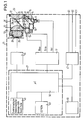
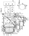
- the core of the color sensor arrangement according to the invention is a tube 36 with a lower receiving projection 37, which are arranged in a rectangular housing 21 made of metal, which can be opened in a suitable manner to introduce the optical, optoelectronic and electronic components to be able to.
- the tube 36 and the receiving projection 37 are preferably designed as a uniform precision injection molded component.
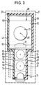
- she 3 have essentially the shape of a box open on one side, which is closed by a cover 43.
- the receiving attachment 37 is, however, significantly narrower than the tube 36, so that at the transition from the receiving attachment 37 to the tube 36 the box has a step 59 and the cover 43 has a step 62.
- the tube 36 has a central cavity 51 which is open at both ends and in which, in FIG. 2, from left to right, one after the other is accommodated: a photo element 26, an annular aperture 25, a lens 24, an IR cut filter 52, a further lens 23 with a larger diameter and a transparent plane-parallel plate 30 inclined at 45 ° to the axis 29 of the condenser lens system 23, 24 or the tube 36, which in the region of the point of intersection of the axis 29 and around it on the side facing away from the condenser lens system 23, 24 a mirror covering 31 is covered.
- the plate 30 with the mirror covering 31 forms a geometric beam splitter 28.
- annular mirror covering 31 ′ which is only indicated by dashed lines in FIG. 2, is provided on the opposite side from the mirror covering 31. It covers those areas of the plate 30 which are permeable in the exemplary embodiment shown in solid lines according to FIG. 2, while in the alternative embodiment the central area which is covered by the mirror covering 31 according to FIG. 2 is permeable.
- a collimator lens 32 is arranged, to which the cavity 42 of the receptacle attachment 37, which is integral with the tube 36, is connected at the bottom.
- two dichroic deflecting mirrors 14 and 15 are arranged at an angle of 45 ° to the axis 16 on its optical axis 16 at a vertical distance.
- the dichroic mirrors 14, 15 are held on the outer walls of the cavity 42 by suitable holders 41 (FIG. 2).
- a receiving space 38 for a further semiconductor radiation source 11 is formed below the dichroic mirror 14, which, for example, emits light in the red spectral range.
- perforated screens 33, 34 and 35 are arranged in the receiving cavities 38, 39, 40, which are concentric with the axis 16 and the axes 53, 54 of the semiconductor radiation sources 12, 13.
- the openings of the perforated screens 38, 39, 40 are rectangular at smaller scanning distances A (FIG. 2) corresponding to the print marks to be recognized and circular at larger scanning distances A.
- a reading area 18 In front of the lens 22 or the housing 21 there is a reading area 18 in which there is an object 20 provided with different color markings 19a, 19b or 19c, the color markings of which are different from those of the invention Color sensor arrangement to be read or recognized.
- the dichroic mirrors 14, 15, the geometric beam splitter 28 and the IR cut filter 52 have a rectangular shape.
- the lenses 23, 24 and 32 are of round design and have rectangular projections 23 ', 23' '(FIGS. 2 and 4), 24', 24 '' and 32 ', 32' 'on two sides, but for optical purposes Do not contribute the image, but perform a pure support function. All of the aforementioned components and also the perforated diaphragms 33, 34, 35 are inserted from the open side into mounting grooves 41 and 57 and pushed in as far as they will go.
- the cover 43 contains corresponding stop formations 60 (FIG. 3) which extend into the tube 36 or the receiving attachment 37 and adjoin the respective optical element, so that after the tube 36 and the receiving attachment 37 have been fully equipped and the clean closing of the cover 43 ensures a correct position of the optical components.
- the lens 22 is circular and inserted into the wall of the housing 21, which is preferably made of metal.
- the tube 36 and the receiving projection 37 are aligned with the housing 21 by means of fitting bores 61 and not shown fitting pins provided on the housing 21.
- the plate 30, which is preferably made of glass, merely serves as a support for the deflecting mirror covering 31 or 31 'and guarantees the correct position of the deflecting mirror in the beam path. 2, the glass plate 30 ends at the top clearly below the upper end of the tube in order to enable a compact relative arrangement of the tube 36 and the objective 22. In order to avoid disturbing reflections, in particular the upper end face of the plate 30 is blackened.
- the lens system 23, 24 is constructed in two stages because a short focal length is to be realized in the present large lens opening.
- the photo element 16 is connected via a preamplifier 45 to an evaluation electronics 27, which has a microprocessor 50, an EEPROM 48 and an operating panel 49 with a function switch, tolerance switch, display LEDs and a teach button.
- the evaluation electronics 27 is fed by a power supply unit 46.
- An output stage 47 connected to the microprocessor 50 supplies the output signals of the color sensor arrangement to output terminals Q1, Q2 and Q3.
- the signals at the output terminals Q1 to Q3 represent three switching outputs.
- the overall color sensor arrangement is designed in such a way that up to three different color patterns can be stored per teach-in, i.e. that the sensor can sort three different colors.
- the corresponding switching output Q1, Q2 or Q3 is activated accordingly by the electronics.
- the semiconductor radiation sources 11, 12, 13 are connected to control electronics 17, which in turn are connected to the microprocessor 50.
- FIG. 3 the electrical and electronic components shown in a schematic, extended block diagram in FIG. 1 are arranged on printed circuit boards 44 which are only indicated by dashed lines and which are accommodated in a very compact design to the side of the receiving attachment 37 in rooms 58 of the cuboid housing 21.
- a further printed circuit board 44 can also be arranged flat, according to FIG. 2, directly behind the photoelement 26 on the left end face of the tube 36 in FIG. 2.
- the semiconductor radiation sources 11, 12, 13 are actuated sequentially by the control electronics 17 such that first the semiconductor radiation source 11 is a red light beam, then the semiconductor radiation source 12 is a green light beam and finally the semiconductor radiation source 13 is a blue light beam along the axes 16, 53 and 54 send out.
- the microprocessor 50 generates pulse widths of less than 10 ⁇ s.
- the successively generated light beams of the semiconductor radiation sources 11, 12 and 13 are directed by means of the dichroic mirrors 14, 15 onto the common optical axis 16, with a suitable length of the receiving cavities 38, 39 and 40, 40 'ensuring that the of Cover the radiation emanating from the semiconductor radiation sources 11, 12 and 13 as far as the collimator lens 32.
- the semiconductor radiation sources 11, 12, 13 used have small radiation angles according to the invention, so that narrowly limited radiation beams are emitted, which are further concentrated on the mirror coating 31 of the beam splitter 23 by the collimator lens 32.
- the transmitted light bundles are deflected by 90 ° in the direction of the optical axis 29 of the objective 22. In this way, a transmitted light bundle 55 extends from the objective 22.
- the collimator lens 32 and the objective 22 form the diaphragms 33, 34, 35 arranged directly in front of the semiconductor radiation sources 11, 12, 13 on the surface of an object 20, which is arranged in the reading area 18 located in front of the housing 21 and bears the color markings 19a, 19b and 19c to be read.
- the transmission light bundles are scattered back from the surface of the object 20 to the lens 22, the part 56 of the reception light bundle which takes up the entire cross section of the lens 22 and which does not fall on the central mirror covering 31, passes through the transparent plate 30 and over the lens system 23. 24 strikes the photo element 26, in front of which the diaphragm 25 is arranged with a square opening.
- the length of the plate 30 upwards is essentially limited by the upper end of the mirror covering 31, so that part of the reception light reaches the lens system 23, 24 at the top past the plate 30.
- the likewise square photo element 26 thus emits an electrical signal which is representative of the light intensity received.
- the electrical signal emitted by the photo element 26 is first amplified in the preamplifier 45 (FIG. 1) and fed to a sample and hold stage and is passed via an analog-digital converter for further digital processing.
- the taught-in signal levels or the upper and lower threshold values calculated from them (corresponding to the selected tolerance and hysteresis) and the system software are stored in the EEPROM 48.
- the receiver delivers the same signal level for all three transmission pulses for a given gray value pattern (eg 90% remission). For any color template, it is checked in RUN mode whether the three received signals match the previously taught-in color of the comparison sample. Then there is agreement reached when the current signal level is within a tolerance band.
- This tolerance band is determined in teach mode according to the size of the respective color values, the required switching hysteresis derived from it (depending on the noise ratios) and the position of the tolerance switch.
- the color sensor arrangement according to the invention is very durable due to the use of semiconductor radiation sources.
- the teach-in button provided for adaptation to different tasks is particularly advantageous.
- a high depth of field is guaranteed due to the collimation of the transmitted radiation.
- High switching frequencies can be used for the semiconductor radiation sources.
- the color sensor arrangement can be used for at least two scanning distances, e.g. 10 mm and 60 mm.
- the autocollimation arrangement according to the invention enables the construction of an extremely compact sensor with a large relative opening.
- the IR blocking filter 52 in the reception path serves to suppress extraneous light.
- the sequential, pulsed operation of the semiconductor radiation sources 11, 12, 13 is also advantageous for this. According to the invention, two or more signal cycles are advantageously logically combined.
- the mirror coverings 31, 31 ' are preferably realized by partial vapor deposition of a transparent support (glass plate), the outer contour of the mirror cover 31 producing the symmetry of the transmission path to the reception path without further suppression.
- all optical and optoelectronic components are fastened to a single housing (tube 36 / receiving attachment 37).
- the tube 36 and the receiving projection 37 are manufactured as a one-piece precision injection-molded part, so that the positions of the components are clearly determined.
- the semiconductor radiation sources 11, 12, 13 and the lenses 32, 23, 24 are precisely fixed by pressing them against a stop by means of displacement lugs.
- the correct position of the lenses and mirrors is checked and ensured by means of the special shape (formations 60) of the cover 43 when the cover is being applied.
- the diaphragms 33, 34, 35 arranged in front of the semiconductor radiation sources 11, 12, 13 are imaged on the object 20, as a result of which an edge-sharp image point is obtained.
- the objective would be tilted to the left by 90 ° in relation to FIG. 2, the optical axis 29 of the objective being brought into alignment with the optical axis 16 of the collimator lens 32 .
- the transmission light initially passes through the central region of the transparent plate 30, while the reception light is reflected by the mirror covering 31 ′ into the lens system 23, 24.
- the use of a geometric beam splitter 28 brings more than 60% signal gain compared to the physical beam splitter.
Abstract
Description
Die Erfindung betrifft eine Farbsensoranordnung zum Lesen farbiger Markierungen nach dem Oberbegriff des Anspruches 1. Besonders bevorzugt werden derartige Farbsensoranordnungen zum Lesen farbiger Druckmarken in kurzem Arbeitsabstand verwendet. Die Farbsensoranordnung ist aber auch für viele weitere Anwendungen geeignet. Hinzuweisen ist hier auf die Auftragskontrolle bzw. -überwachung von Spendevorgängen (Sicherungslack), Banderolen-, Etiketten- oder Markierungserkennung sowie die Überwachung von Beschichtungsprozessen. In Frage kommt die Anwendung auch bei der Anwesenheitsprüfung von Gegenständen. Im allgemeinen werden zwei Versionen mit 10 mm oder 60 mm Tastabstand zur Verfügung gestellt.The invention relates to a color sensor arrangement for reading colored markings according to the preamble of claim 1. Such color sensor arrangements are particularly preferably used for reading colored print marks in a short working distance. The color sensor arrangement is also suitable for many other applications. Reference should be made here to the order control or monitoring of dispensing processes (security lacquer), banderole, label or marking recognition and the monitoring of coating processes. It can also be used for checking the presence of objects. In general, two versions with 10 mm or 60 mm scanning distance are available.
Das Ziel der Erfindung besteht darin, eine derartige Farbsensoranordnung so weiterzubilden, daß sie mit bestehenden Kontrasttastern kurzer Tastweite kompatibel sind und die Gehäuseabmessungen eines Kontrasttasters nach Möglichkeit beibehalten werden, d.h., daß die größere Anzahl von optischen und optoelektronischen Bauelementen bei einer Farbsensoranordnung auf möglichst kleinem Raum untergebracht ist, wobei aber die hohen Anforderungen an die Präzision der Anordnung der optischen und optoelektronischen Bauelemente voll erfüllt werden.The aim of the invention is to develop such a color sensor arrangement in such a way that they are compatible with existing contrast sensors with a short scanning range and the housing dimensions of a contrast sensor are retained as far as possible, that is to say that the larger number of optical and optoelectronic components in a color sensor arrangement takes up as little space as possible is housed, but the high demands on the precision of the arrangement of the optical and optoelectronic components are fully met.
Zur Lösung dieser Aufgabe sind die Merkmale des kennzeichnenden Teils des Anspruches 1 vorgesehen.To achieve this object, the features of the characterizing part of claim 1 are provided.
Erfindungsgemäß wird also mit einer Autokollimationsanordnung gearbeitet, wobei zur Reduzierung des optischen Übersprechens ein geometrischer Strahlteiler verwendet wird. Auf diese Weise wird auch das optische Übersprechen durch Verschmutzung der nach außen liegenden Objektivlinsenfläche innerhalb des Beleuchtungskegels infolge der vorzugsweise zentral auftretenden Abschattung reduziert.According to the invention, an autocollimation arrangement is therefore used, a geometric beam splitter being used to reduce the optical crosstalk. In this way, the optical crosstalk is also reduced due to the contamination of the outwardly lying objective lens surface within the illumination cone as a result of the preferably central shadowing.
Zur Reduzierung des optischen Übersprechens wird weiter vorzugsweise das Objektiv beidseitig über die gesamte spektrale Bandbreite der verwendeten Halbleiterstrahlungsquellen entspiegelt.To reduce the optical crosstalk, the objective is further preferably antireflected on both sides over the entire spectral bandwidth of the semiconductor radiation sources used.
Die gezielte Verwendung von leistungsstarken LED's mit kleinem Abstrahlwinkel als Halbleiterstrahlungsquellen hat zur Folge, daß die Sendeöffnung im Vergleich zur Empfangsöffnung deutlich kleiner ausgebildet sein kann. Insofern bietet der erfindungsgemäß verwendete Strahlteiler auch erhebliche Vorteile in der Leistungsbilanz.The targeted use of powerful LEDs with a small beam angle as semiconductor radiation sources has the consequence that the transmission opening can be made significantly smaller compared to the reception opening. In this respect, the beam splitter used according to the invention also offers considerable advantages in the power balance.
Der geometrische Strahlteiler ist vorteilhaft gemäß Anspruch 2 ausgebildet, wobei der Spiegelbelag gemäß den Ansprüchen 3 oder 4 angeordnet sein kann.The geometric beam splitter is advantageously designed according to claim 2, wherein the mirror covering can be arranged according to claims 3 or 4.
Bei der Ausführungsform nach Anspruch 3 wird lediglich derjenige zentrale Bereich der Platte mit einem Spiegelbelag versehen, der von dem schmalen Sendelichtbündel der Halbleiterstrahlungsquellen getroffen wird.In the embodiment according to claim 3, only that central region of the plate is provided with a mirror coating which is hit by the narrow beam of transmitted light from the semiconductor radiation sources.
Bei der Ausführungsform nach Anspruch 4 gehen die Sendelichtbündel der Halbleiterstrahlungsquellen durch die Platte hindurch, während das Empfangslicht vom Spiegelbelag zur Empfangsanordnung ausgespiegelt wird.In the embodiment according to claim 4, the transmitted light beams of the semiconductor radiation sources pass through the plate, while the received light is reflected from the mirror coating to the receiving arrangement.
Eine baulich besonders kompakte Anordnung wird durch die Maßnahmen nach den Ansprüchen 5 und 6 erzielt. Auf diese Weise werden die Vorteile der Verwendung von dichroitischen Spiegeln bei baulicher Kompaktheit erzielt.A structurally particularly compact arrangement is achieved by the measures according to claims 5 and 6. In this way, the advantages of using dichroic mirrors are achieved with a compact structure.
Besonders vorteilhaft ist eine Ausbildung mit drei Halbleiterstrahlungsquellen in den drei Grundfarben, welche zweckmäßig nach Anspruch 7 angeordnet sind, um einerseits eine kompakte Unterbringung und andererseits gleiche optische Wege für die Strahlungen der verschiedenen Halbleiterstrahlungsquellen zu erzielen. Hierbei wird vorteilhafterweise nach Anspruch 8 vorgegangen.A design with three semiconductor radiation sources in the three primary colors, which are expediently arranged according to claim 7, is particularly advantageous in order to provide compact accommodation on the one hand and the same optical appearance on the other To achieve ways for the radiation of the various semiconductor radiation sources. This is advantageously carried out according to claim 8.
Durch die Maßnahme nach Anspruch 9 wird vorteilhafterweise eine Konzentration des Sendelichtes auf dem Strahlteiler erzielt, was einerseits einer exakten geometrischen Strahlungstrennung und andererseits einer günstigen Energiebilanz zugutekommt.The measure according to claim 9 advantageously achieves a concentration of the transmitted light on the beam splitter, which benefits on the one hand an exact geometric radiation separation and on the other hand a favorable energy balance.
Um einen randscharfen Bildpunkt auf den mit den Markierungen versehenen Gegenständen zu erzielen, sind erfindungsgemäß zweckmäßig die Blenden nach Anspruch 10 vorgesehen.In order to achieve a sharp image point on the objects provided with the markings, the diaphragms according to claim 10 are expediently provided according to the invention.
Von besonderem Vorteil ist die Ausbildung nach Anspruch 11 und 12, weil hierdurch alle wichtigen Bauelemente zu einer einzigen kompakten Anordnung in präziser Weise zusammengefaßt werden.The embodiment according to
Für die Montage ist die Ausbildung nach den Ansprüchen 13 oder 14 von Vorteil, weil dannn die einzelnen Bauelemente vor dem Aufbringen des Deckels von der offenen Seite her in geeignet angeordnete Nuten in den als Präzisions-Spritzgußteil hergestellten Tubus mit Aufnahmeansatz eingeschoben und so präzise angeordnet werden können, um anschließend durch Aufbringen des Deckels in dieser Präzisionsanordnung der einzelnen Bauelemente fixiert zu werden. Durch das Aufbringen des Deckels entsteht ein geschlossesner Kasten, der lediglich fünf seitliche Öffnungen für die drei LED's, den Empfänger und das Objektiv enthält.For the assembly, the design according to
Insbesondere für die Montage ist die Rechteckform der meisten optischen und optoelektronischen Bauelemente gemäß Anspruch 15 zweckmäßig. Kreisförmige Linsen können durch Ausbildung nach Anspruch 16 in dieses System einbezogen werden.The rectangular shape of most optical and optoelectronic components is particularly expedient for assembly. Circular lenses can be included in this system by training according to
Die kompakte Ausbildung der erfindungsgemäßen Farbsensoranordnung wird weiter durch die Ausbildung nach Anspruch 17 gefördert. Erfindungsgemäß wird also der durch das gegenüber dem Empfangslichtbündel schmälere Sendelichtbündel frei werdende Platz für die Unterbringung der Leiterplatten genutzt.The compact design of the color sensor arrangement according to the invention is further promoted by the design according to
Die Erfindung wird im folgenden beispielsweise anhand der Zeichnung beschrieben; in dieser zeigt:
- Fig. 1
- eine schematische teilweise geschnittene und teilweise blockschaltbildartige Darstellung einer erfindungsgemäßen Farbsensoranordnung,
- Fig. 2
- eine vergrößerte Schnittansicht des optischen Teils der erfindungsgemäßen Farbsensoranordnung,
- Fig. 3
- eine schematische Vorderansicht des Gegenstandes der Fig. 2 in Richtung des Pfeiles III ohne das Objektiv und
- Fig. 4
- die Draufsicht einer kreisförmigen Linse mit rechteckförmigen Ansätzen.
- Fig. 1
- 2 shows a schematic, partially sectioned and partially block diagram-like illustration of a color sensor arrangement according to the invention,
- Fig. 2
- 2 shows an enlarged sectional view of the optical part of the color sensor arrangement according to the invention,
- Fig. 3
- is a schematic front view of the object of FIG. 2 in the direction of arrow III without the lens and
- Fig. 4
- the top view of a circular lens with rectangular approaches.
In allen Figuren bezeichnen gleiche Bezugszahlen entsprechende Bauelemente.In all figures, the same reference numbers denote corresponding components.
Nach den Fig. 1 bis 3 ist das Kernstück der erfindungsgemäßen Farbsensoranordnung ein Tubus 36 mit einem unteren Aufnahmeansatz 37, die in einem quaderförmigen Gehäuse 21 aus Metall angeordnet sind, welches in geeigneter Weise geöffnet werden kann, um die optischen, optoelektronischen und elektronischen Bauelemente einbringen zu können. Der Tubus 36 und der Aufnahmeansatz 37 sind vorzugsweise als einheitliches Präzisions-Spritzgußbauteil ausgebildet. Sie weisen nach Fig. 3 im wesentlichen die Form eines einseitig offenen Kastens auf, der durch einen Deckel 43 verschlossen ist. Der Aufnahmeansatz 37 ist jedoch deutlich schmäler als der Tubus 36 ausgebildet, so daß am Übergang vom Aufnahmeansatz 37 zum Tubus 36 der Kasten eine Stufe 59 und der Deckel 43 eine Stufe 62 aufweist.1 to 3, the core of the color sensor arrangement according to the invention is a
Der Tubus 36 weist einen an beiden Enden offenen zentralen Hohlraum 51 auf, in welchem in Fig. 2 von links nach rechts gesehen hintereinander untergebracht sind: ein Photoelement 26, eine Kreisringblende 25, eine Linse 24, ein IR-Sperrfilter 52, eine weitere Linse 23 mit größerem Durchmesser und ein unter 45° zur Achse 29 des Kondensorlinsensystems 23, 24 bzw. des Tubus 36 geneigte transparente planparallele Platte 30, die im Bereich des Durchstoßpunktes der Achse 29 und um diese herum auf der vom Kondensorlinsensystem 23, 24 abgewandten Seite mit einem Spiegelbelag 31 bedeckt ist. Die Platte 30 mit dem Spiegelbelag 31 bildet einen geometrischen Strahlteiler 28.The
Bei einer alternativen Ausführungsform ist ein in Fig. 2 nur gestrichelt angedeuteter kreisringförmiger Spiegelbelag 31' auf der entgegengesetzten Seite wie der Spiegelbelag 31 vorgesehen. Er deckt diejenigen Bereiche der Platte 30 ab, die beim in ausgezogenen Linien wiedergegebenen Ausführungsbeispielen nach Fig. 2 durchlässig sind, während bei der alternativen Ausführungsform der zentrale Bereich, der nach Fig.2 durch den Spiegelbelag 31 abgedeckt ist, durchlässig ist.In an alternative embodiment, an annular mirror covering 31 ′, which is only indicated by dashed lines in FIG. 2, is provided on the opposite side from the mirror covering 31. It covers those areas of the
Auf der vom Kondensorlinsensystem 23, 24 abgewandten Seite des Strahlteilers 28 befindet sich ein Front-Objektiv 22, welches in einer Stirnwand des nur gestrichelt angedeuteten Gehäuses 21 eingebaut ist.On the side of the
In der unteren Wand des Tubus 36 ist unterhalb des Spiegelbelages 31 eine Kollimatorlinse 32 angeordnet, an die nach unten der Hohlraum 42 des mit dem Tubus 36 einstückigen Aufnahmeansatzes 37 anschließt.In the lower wall of the
Unter der Kollimatorlinse 32 sind auf deren optischer Achse 16 im vertikalen Abstand zwei dichroitische Umlenkspiegel 14 bzw. 15 unter einem Winkel von 45° zur Achse 16 angeordnet. Die dichroitischen Spiegel 14, 15 sind durch geeignete Halterungen 41 (Fig. 2) an den Außenwänden des Hohlraums 42 gehalten.Under the
Hinter den dichroitischen Spiegeln 14, 15 sind in Richtung des Linsensystems 23, 24 an den Hohlraum 42 anschließende Aufnahmeräume 39 bzw. 40, 40' vorgesehen, in denen Halbleiterstrahlungsquellen 12 bzw. 13 z.B. für die Farben grün und blau befestigt sind.Behind the
In Ausrichtung mit der Achse 16 ist unterhalb des dichroitischen Spiegels 14 ein Aufnahmeraum 38 für eine weitere Halbleiterstrahlungsquelle 11 ausgebildet, welche beispielsweise Licht im roten Spektralbereich aussendet.In alignment with the
Unmittelbar vor den Halbleiterstrahlungsquellen 11, 12, 13 sind jeweils Lochblenden 33, 34 bzw. 35 in den Aufnahmehohlräumen 38, 39, 40 angeordnet, welche konzentrisch mit der Achse 16 bzw. den Achsen 53, 54 der Halbleiterstrahlungsquellen 12, 13 sind. Die Öffnungen der Lochblenden 38, 39, 40 sind bei geringeren Tastabständen A (Fig. 2) entsprechend den zu erkennenden Druckmarken rechteckförmig und bei größeren Tastabständen A kreisförmig.Immediately in front of the
Vor dem Objektiv 22 bzw. dem Gehäuse 21 befindet sich ein Lesebereich 18, in welchem sich ein mit unterschiedlichen Farbmarkierungen 19a, 19b bzw. 19c versehener Gegenstand 20 befindet, dessen Farbmarkierungen von der erfindungsgemäßen Farbsensoranordnung gelesen bzw. erkannt werden sollen.In front of the
Die dichroitischen Spiegeln 14, 15, der geometrische Strahlteiler 28 und der IR-Sperrfilter 52 haben Rechteckform. Die Linsen 23, 24 und 32 sind von runder Bauform und besitzen an zwei Seiten rechteckförmige Ansätze 23', 23'' (Fig. 2 und 4), 24', 24'' und 32', 32'', die jedoch zur optischen Abbildung nicht beitragen, sondern eine reine Halterungsfunktion ausüben. Alle zuvorgenannten Komponenten und auch die Lochblenden 33, 34, 35 werden von der offenen Seite her in Halterungsnuten 41 bzw. 57 eingeführt und bis auf Anschlag hineingeschoben. Der Deckel 43 enthält im Bereich der jeweiligen optischen Komponente entsprechende Anschlagausformungen 60 (Fig. 3), die in den Tubus 36 bzw. den Aufnahmeansatz 37 hineinreichen und an das jeweilige optische Element angrenzen, so daß nach vollständiger Bestückung des Tubus 36 und des Aufnahmeansatzes 37 und das saubere Schließen des Deckels 43 eine korrekte Position der optischen Komponenten gewährleistet ist.The
Das Objektiv 22 ist kreisförmig ausgebildet und in die Wand des vorzugsweise aus Metall bestehenden Gehäuses 21 eingesetzt. Der Tubus 36 und der Aufnahmeansatz 37 sind mittels Paßbohrungen 61 und nicht dargestellter, am Gehäuse 21 vorgesehener Paßzapfen definiert zum Gehäuse 21 ausgerichtet.The
Die vorzugsweise aus Glas bestehende Platte 30 dient lediglich als Träger für den Umlenk-Spiegelbelag 31 bzw. 31' und garantiert die korrekte Lage des Umlenkspiegels im Strahlengang. Nach Fig. 2 endet die Glasplatte 30 oben deutlich unterhalb des oberen Endes des Tubus, um eine kompakte Relativanordnung des Tubus 36 und des Objektivs 22 zu ermöglichen. Um störende Reflexe zu vermeiden, wird insbesondere die obere Stirnseite der Platte 30 geschwärzt.The
Das Linsensystem 23, 24 ist deswegen zweistufig aufgebaut, weil bei der vorliegenden großen Linsenöffnung eine kurze Brennweite realisiert werden soll.The
Nach Fig. 1 ist das Photoelement 16 über einen Vorverstärker 45 an eine Auswerteelektronik 27 angeschlossen, die einen Mikroprozessor 50, ein EEPROM 48 und ein Bedienungsfeld 49 mit Funktionsschalter, Toleranzschalter, Anzeige-LED's und einer Teach-Taste aufweist. Die Auswerteelektronik 27 wird von einem Netzteil 46 gespeist. Eine an den Mikroprozessor 50 angeschlossene Ausgangsstufe 47 liefert die Ausgangssignale der Farbsensoranordnung an Ausgangsklemmen Q1, Q2 und Q3.1, the
Die Signale an den Ausgangsklemmen Q1 bis Q3 stellen drei Schaltausgänge dar. Die Farbsensoranordnung ist insgesamt derart ausgelegt, daß bis zu drei verschiedene Farbmuster pro Teach-In gespeichert werden können, d.h. daß der Sensor Sortiervorgänge bezüglich drei unterschiedlicher Farben vornehmen kann. Der entsprechende Schaltausgang Q1, Q2 bzw. Q3 wird bei Übereinstimmung durch die Elektronik entsprechend aktiviert.The signals at the output terminals Q1 to Q3 represent three switching outputs. The overall color sensor arrangement is designed in such a way that up to three different color patterns can be stored per teach-in, i.e. that the sensor can sort three different colors. The corresponding switching output Q1, Q2 or Q3 is activated accordingly by the electronics.
Die Halbleiterstrahlungsquellen 11, 12, 13 sind an eine Ansteuerungselektronik 17 angeschlossen, die ihrerseits mit dem Mikroprozessor 50 verbunden ist.The
Nach Fig. 3 sind die in Fig. 1 in einem nur schematischen, ausgedehnten Blockschaltbild gezeigten elektrischen und elektronischen Bauelemente auf nur gestrichelt angedeuteten Leiterplatten 44 angeordnet, welche in sehr kompakter Bauweise seitlich des Aufnahmeansatzes 37 in Räumen 58 des quaderförmigen Gehäuses 21 untergebracht sind. Eine weitere Leiterplatte 44 kann auch gemaß Fig. 2 unmittelbar hinter dem Photoelement 26 flach an der in Fig. 2 linken Stirnseite des Tubus 36 angeordnet sein.According to FIG. 3, the electrical and electronic components shown in a schematic, extended block diagram in FIG. 1 are arranged on printed
Die exakte Anordnung und Dimensionierung insbesondere der optischen und optoelektronischen Bauelemente ergeben sich aus der folgenden Funktionsbeschreibung.The exact arrangement and dimensions, in particular of the optical and optoelectronic components, result from the following functional description.
Die Halbleiterstrahlungsquellen 11, 12, 13 werden von der Ansteuerungselektronik 17 sequentiell angesteuert, derart, daß zunächst die Halbleiterstrahlungsquelle 11 ein rotes Lichtbündel, dann die Halbleiterstrahlungsquelle 12 ein grünes Lichtbündel und schließlich die Halbleiterstrahlungsquelle 13 ein blaues Lichtbündel entlang der Achsen 16, 53 bzw. 54 aussenden. Durch den Mikroprozessor 50 werden Impulsbreiten kleiner als 10 µs generiert.The
Die nacheinander erzeugten Lichtbündel der Halbleiterstrahlungsquellen 11, 12 bzw. 13 werden mittels der dichroitischen Spiegel 14, 15 auf die gemeinsame optische Achse 16 gelenkt, wobei durch geeignete Länge der Aufnahmehohlräume 38, 39 bzw. 40, 40' dafür gesorgt wird, daß die von den Halbleiterstrahlungsquellen 11, 12 bzw. 13 ausgehende Strahlung bis zur Kollimatorlinse 32 gleiche Wegstrecken zurücklegen.The successively generated light beams of the
Die verwendeten Halbleiterstrahlungsquellen 11, 12, 13 weisen erfindungsgemäß kleine Abstrahlwinkel auf, so daß eng begrenzte Strahlungsbündel ausgesendet werden, die durch die Kollimatorlinse 32 weiter auf den Spiegelbelag 31 des Strahlteilers 23 konzentriert wird. Am Strahlteiler 28 erfolgt eine Umlenkung der Sende-Lichtbündel um 90° in Richtung der optischen Achse 29 des Objektivs 22. Auf diese Weise geht vom Objektiv 22 ein Sendelichtbündel 55 aus.The
Die Kollimatorlinse 32 und das Objektiv 22 bilden die unmittelbar vor den Halbleiterstrahlungsquellen 11, 12, 13 angeordneten Blenden 33, 34, 35 auf der Oberfläche eines Gegenstandes 20 ab, der in dem vor dem Gehäuse 21 befindlichen Lesebereich 18 angeordnet ist und die zu lesenden Farbmarkierungen 19a, 19b und 19c trägt.The
Von der Oberfläche des Gegenstandes 20 werden die Sendelichtbündel zurück zum Objektiv 22 gestreut, wobei der Teil 56 des den gesamten Querschnitt des Objektivs 22 einnehmenden Empfangslichtbündels, der nicht auf den zentralen Spiegelbelag 31 fällt, durch die transparente Platte 30 hindurchgeht und über das Linsensystem 23, 24 auf das Photoelement 26 auftrifft, vor dem die Blende 25 mit quadratischer Öffnung angeordnet ist. Die Länge der Platte 30 nach oben ist im wesentlichen durch das obere Ende des Spiegelbelages 31 begrenzt, so daß ein Teil des Empfangslichtes oben an der Platte 30 vorbei zum Linsensystem 23, 24 gelangt.The transmission light bundles are scattered back from the surface of the
Das ebenfalls quadratische Photoelement 26 gibt somit ein elektrisches Signal ab, welches für die empfangene Lichtintensität repräsentativ ist. Das vom Photoelement 26 abgegebene elektrische Signal wird zunächst im Vorverstärker 45 (Fig. 1) verstärkt und einer Sample & Hold-Stufe zugeführt sowie zwecks digitaler Weiterverarbeitung über einen Analog-Digital-Wandler geführt.The likewise
In dem EEPROM 48 sind die eingelernten Signalpegel bzw. die daraus berechneten oberen und unteren Schwellenwerte (entsprechend der gewählten Toleranz und Hysterese) abgelegt sowie die Systemsoftware.The taught-in signal levels or the upper and lower threshold values calculated from them (corresponding to the selected tolerance and hysteresis) and the system software are stored in the
In der Grundeinstellung liefert der Empfänger bei einem vorgegebenen Grauwertmuster (z.B. 90% Remission) für alle drei Sendeimpulse einen gleichen Signalpegel. Für eine beliebige Farbvorlage wird im RUN-Modus geprüft, ob die drei Empfangssignale mit der zuvor eingelernten Farbe des Vergleichsmusters übereinstimmen. Übereinstimmung ist dann erreicht, wenn der aktuelle Signalpegel innerhalb eines Toleranzbandes liegt. Dieses Toleranzband wird im Teach-Modus entsprechend der Größe der jeweiligen Farbwerte, der daraus abgeleiteten erforderlichen Schalthysterese (abhängig von den Rauschverhältnissen) und der Stellung des Toleranzschalters ermittelt.In the basic setting, the receiver delivers the same signal level for all three transmission pulses for a given gray value pattern (eg 90% remission). For any color template, it is checked in RUN mode whether the three received signals match the previously taught-in color of the comparison sample. Then there is agreement reached when the current signal level is within a tolerance band. This tolerance band is determined in teach mode according to the size of the respective color values, the required switching hysteresis derived from it (depending on the noise ratios) and the position of the tolerance switch.
Im RUN-Modus wird auf den bereits im Teach-Modus vorbestimmten maximalen Farbwert normiert. Die Normierung auf den im Teachvorgang ermittelten maximalen Farbwert bietet folgende Vorteile:
- Signalschwankungen durch unterschiedliche Tastebenen bzw. durch die Temperaturabhängigkeit der Strahlstärke der einzelnen Strahlungsquellen werden eliminiert, sofern sich die Schwankungen für alle Strahlungsquellen gleichartig verhalten.
- Nichtfarbige Objekte bzw. unterschiedlich gesättigte Farbwerte sind aus dem Normierungsergebnis unmittelbar ableitbar und werden korrekt erkannt.
- Höchste Auflösung bezüglich Farbsättigung.
- Zeitoptimales Normierungsverfahren.
- Geringer Einfluß des Rauschpegels.
- Signal fluctuations due to different touch levels or the temperature dependence of the radiation intensity of the individual radiation sources are eliminated, provided the fluctuations behave in the same way for all radiation sources.
- Non-colored objects or differently saturated color values can be derived directly from the standardization result and are recognized correctly.
- Highest resolution in terms of color saturation.
- Time-optimized standardization procedure.
- Little influence of the noise level.
Die erfindungsgemäße Farbsensoranordnung ist aufgrund der Verwendung von Halbleiterstrahlungsquellen sehr langlebig. Von besonderem Vorteil ist die einer Anpassung an verschiedene Aufgaben vorgesehene Teach-In-Taste. Aufgrund der Kollimation der Sendestrahlung ist eine hohe Tiefenschärfe gewährleistet. Es können für die Halbleiterstrahlungsquellen hohe Schaltfrequenzen verwendet werden.The color sensor arrangement according to the invention is very durable due to the use of semiconductor radiation sources. The teach-in button provided for adaptation to different tasks is particularly advantageous. A high depth of field is guaranteed due to the collimation of the transmitted radiation. High switching frequencies can be used for the semiconductor radiation sources.
Durch Auswechslung des Objektivs 22 kann die Farbsensoranordnung für mindestens zwei Tastweiten, z.B. 10 mm und 60 mm, ausgelegt werden.By changing the
Die erfindungsgemäße Autokollimationsanordnung ermöglicht den Aufbau eines äußerst kompakten Sensors bei großer relativer Öffnung.The autocollimation arrangement according to the invention enables the construction of an extremely compact sensor with a large relative opening.
Das IR-Sperrfilter 52 im Empfangspfad (Fig. 2) dient der Fremdlichtunterdrückung. Hierzu ist auch der sequentielle, gepulste Betrieb der Halbleiterstrahlungsquellen 11, 12, 13 von Vorteil. Zweckmäßigerweise findet erfindungsgemäß eine logische Verknüpfung von zwei bzw. mehreren Signalzyklen statt.The
Die Spiegelbeläge 31, 31' werden bevorzugt im Wege der Teilbedampfung eines transparenten Trägers (Glasplatte) verwirklicht, wobei die Außenkontur des Spiegelbelages 31 die Symmetrie des Sendepfades zum Empfangspfad ohne weitere Ausblendung herstellt.The
Erfindungsgemäß sind alle optischen und optoelektronischen Komponenten an einem einzigen Gehäuse (Tubus 36/Aufnahmeansatz 37) befestigt.According to the invention, all optical and optoelectronic components are fastened to a single housing (
Der Tubus 36 und der Aufnahmeansatz 37 sind als ein einteiliges Präzisionsspritzteil gefertigt, so daß die Positionen der Komponenten eindeutig bestimmt sind.The
Die Halbleiterstrahlungsquellen 11, 12, 13 und die Linsen 32, 23, 24 sind durch Andrücken an einen Anschlag mittels Verdrängungsnasen präzise fixiert. Die korrekte Position der Linsen und Spiegel wird über die spezielle Formgebung (Ausformungen 60) des Deckels 43 beim Aufbringen des Deckels kontrolliert und sichergestellt.The
Die vor den Halbleiterstrahlungsquellen 11, 12, 13 angeordneten Blenden 33, 34, 35 werden auf den Gegenstand 20 abgebildet, wodurch ein randscharfer Bildpunkt erhalten wird.The
Bei der alternativen Ausführungsform mit dem kreisringförmigen Spiegelbelag 31' (Fig. 2) wäre das Objektiv gegenüber Fig.2 um 90° nach links zu kippen, wobei die optische Achse 29 des Objektivs mit der optischen Achse 16 der Kollimatorlinse 32 in Ausrichtung zu bringen ist. Bei dieser Ausführungsform geht das Sendelicht zunächst durch den zentralen Bereich der transparenten Platte 30 hindurch, während das Empfangslicht vom Spiegelbelag 31' in das Linsensystem 23, 24 gespiegelt wird.In the alternative embodiment with the circular mirror covering 31 '(FIG. 2), the objective would be tilted to the left by 90 ° in relation to FIG. 2, the
Bei einem bevorzugten Verhältnis der Pupillendurchmesser (Objektivlinse 22 zur Kollimatorlinse 32) von 2,5 bringt die Verwendung eines geometrischen Strahlteilers 28 im Vergleich zum physikalischen Strahlteiler mehr als 60% Signalgewinn.With a preferred ratio of the pupil diameter (
- 1111
- rote Halbleiterstrahlungsquellered semiconductor radiation source
- 1212th
- grüne Halbleiterstrahlungsquellegreen semiconductor radiation source
- 1313
- blaue Halbleiterstrahlungsquelleblue semiconductor radiation source
- 1414
- dichroitischer Umlenkspiegeldichroic deflecting mirror
- 1515
- dichroitischer Umlenkspiegeldichroic deflecting mirror
- 1616
- gemeinsame optische Achsecommon optical axis
- 1717th
- AnsteuerungselektronikControl electronics
- 1818th
- LesebereichReading area
- 19a19a
- FarbmarkierungenColor markings
- 19b19b
- FarbmarkierungenColor markings
- 19c19c
- FarbmarkierungenColor markings
- 2020th
- Gegenstandobject
- 2121
- Gehäusecasing
- 2222
- Objektivlens
- 2323
- Linselens
- 23'23 '
- rechteckförmiger Ansatzrectangular approach
- 23''23 ''
- rechteckförmiger Ansatzrectangular approach
- 2424th
- Linselens
- 24'24 '
- rechteckförmiger Ansatzrectangular approach
- 24''24 ''
- rechteckförmiger Ansatzrectangular approach
- 2525th
- Blendecover
- 2626
- PhotoelementPhotoelement
- 2727
- AuswertelektronikEvaluation electronics
- 2828
- StrahlteilerBeam splitter
- 2929
- ObjektivachseLens axis
- 3030th
- transparente planparallele Plattetransparent plane-parallel plate
- 3131
- SpiegelbelagMirror covering
- 31'31 '
- SpiegelbelagMirror covering
- 3232
- KollimatorlinseCollimator lens
- 32'32 '
- rechteckförmiger Ansatzrectangular approach
- 32''32 ''
- rechteckförmiger Ansatzrectangular approach
- 3333
- LochblendePinhole
- 3434
- LochblendePinhole
- 3535
- LochblendePinhole
- 3636
- TubusTube
- 3737
- AufnahmeansatzApproach
- 3838
- AufnahmeraumRecording room
- 3939
- AufnahmeraumRecording room
- 40, 40'40, 40 '
- AufnahmeraumRecording room
- 4141
- HalterungsnutenMounting grooves
- 4242
- Hohlraumcavity
- 4343
- Deckelcover
- 4444
- LeiterplatteCircuit board
- 4545
- VorverstärkerPreamplifier
- 4646
- Netzteilpower adapter
- 4747
- AusgangsstufeOutput stage
- 4848
- EEPROMEEPROM
- 4949
- BedienungsfeldControl panel
- 5050
- Mikroprozessormicroprocessor
- 5151
- Hohlraumcavity
- 5252
- IR-SperrfilterIR cut filter
- 5353
- Achseaxis
- 5454
- Achseaxis
- 5555
- SendelichtbündelBeam of light
- 5656
- EmpfangslichtbündelReception light bundle
- 5757
- HaltenutenHolding grooves
- 5858
- Raumroom
- 5959
- Stufestep
- 6060
- AnschlagausformungenStop forms
- 6161
- PaßbohrungenFitting holes
- 6262
- Stufestep
- AA
- TastabstandSensing distance
- Q1Q1
- AusgangsklemmeOutput terminal
- Q2Q2
- AusgangsklemmeOutput terminal
- Q3Q3
- AusgangsklemmeOutput terminal
Claims (10)
dadurch gekennzeichnet,
daß die Strahlungsempfangsanordnung aus dem die Sendestrahlung in den Lesebereich (18) übertragenden Objektiv (22), einem vom Lesebereich (18) aus gesehen dahinter angeordneten geometrischen Strahlteiler (28), welcher innerhalb des Gehäuses (21) Sende- und Empfangsstrahlung trennt, einem hinter dem Strahlteiler (28) vorgesehenen Linsensystem (23, 24) und einem Photoelement (26) besteht, welches die durch den Strahlteiler (28) hindurch auf das Linsensystem (23, 24) treffende und vom Linsensystem (23, 24) konzentrierte Empfangsstrahlung aufnimmt, um daraus ein entsprechendes elektrisches Signal zu bilden, welches der Auswerteelektronik (27) zugeführt ist.Color sensor arrangement for reading colored markings, in particular colored codes and / or printed marks with several, preferably three, semiconductor radiation sources (11, 12, 13) arranged in a housing (21) with different spectral ranges, preferably red, green or blue, the radiation of which by at least one, preferably two dichroic deflecting mirrors (14, 15) matched to the mirrored or transmitted radiation is first directed onto a common optical axis (16) and then via a lens (22) provided on the housing (21) into a reading area (18) and which are preferably controlled sequentially by control electronics (17), which are preferably likewise arranged in the housing (21), and with a photoelectric radiation receiving arrangement (22, 23, 24) provided in the housing (21), which receives radiation reflected from the reading area (18) and evaluation electronics (27), which are preferably also accommodated in the housing (21) hrt, optionally evaluates in cooperation with the control electronics (17) the received radiation,
characterized,
that the radiation receiving arrangement consists of the objective (22) transmitting the transmitted radiation into the reading area (18), a geometrical beam splitter (28) arranged behind it from the reading area (18), which separates transmitting and receiving radiation inside the housing (21), one behind the beam splitter (28) provided lens system (23, 24) and a photo element (26) which through the beam splitter (28) receives reception radiation which strikes the lens system (23, 24) and is concentrated by the lens system (23, 24) in order to form a corresponding electrical signal which is fed to the evaluation electronics (27).
dadurch gekennzeichnet,
daß der Strahlteiler (28) eine vorzugsweise unter einem Winkel von ungefähr 45° zur gemeinsamen optischen Achse (16) der Halbleiterstrahlungsquellen (11, 12, 13) und zur Objektivachse (29) angeordnete transparente planparallele Platte (30) ist, die bereichsweise mit einem Spiegelbelag (31, 31') für die Sende- oder Empfangsstrahlung versehen ist, wobei insbesondere für die Sendestrahlung der Spiegelbelag (31) in Verlängerung der gemeinsamen Achse (16) zentral an der Platte (30) und das Objektiv (22) unter einem rechten Winkel zur gemeinsamen Achse (16) vorgesehen ist oder für die Empfangsstrahlung der Spiegelbelag (31') als Ring um den in der Verlängerung der gemeinsamen Achse (16) liegenden zentralen Bereich der Platte (30) und das Objektiv (22) in Richtung der gemeinsamen Achse (16) vorgesehen ist.Color sensor arrangement according to claim 1,
characterized,
that the beam splitter (28) is a transparent plane-parallel plate (30) which is preferably arranged at an angle of approximately 45 ° to the common optical axis (16) of the semiconductor radiation sources (11, 12, 13) and to the objective axis (29) and which in some areas has a Mirror covering (31, 31 ') is provided for the transmission or reception radiation, the mirror covering (31) in particular in the extension of the common axis (16) centrally on the plate (30) and the objective (22) under a right one for the transmission radiation An angle to the common axis (16) is provided or for the receiving radiation the mirror covering (31 ') as a ring around the central region of the plate (30) lying in the extension of the common axis (16) and the lens (22) in the direction of the common one Axis (16) is provided.
dadurch gekennzeichnet,
daß eine Halbleiterstrahlungsquelle (11) auf der gemeinsamen Achse (16) angeordnet ist, wobei insbesondere wenigstens eine weitere Halbleiterstrahlungsquelle (12; 13) zumindest im wesentlichen senkrecht zur gemeinsamen Achse und auf der dem Empfangs-Linsensystem (23, 24) zugewandten Seite des bzw. der dichroitischen Umlenkspiegel (14; 15) vorgesehen ist.Color sensor arrangement according to one of the preceding claims,
characterized,
that a semiconductor radiation source (11) is arranged on the common axis (16), in particular at least one further semiconductor radiation source (12; 13) at least substantially perpendicular to the common axis and on the side of the receiving lens system (23, 24) facing the the dichroic deflecting mirror (14; 15) is provided.
dadurch gekennzeichnet,
daß zwischen der ersten Halbleiterstrahlungsquelle (11) und dem Strahlenteiler (28) hintereinander zwei dichroitische Spiegel (14, 15) und auf deren dem Empfangslinsensystem (23, 24) zugewandten Seiten in Richtung der gemeinsamen Achse (16) versetzt zwei Halbleiterstrahlungsquellen (12, 13) in entsprechendem Abstand neben- bzw. übereinander angeordnet sind, wobei insbesondere die zweite und dritte Halbleiterstrahlungsquelle (12; 13) in Richtung der Objektivachse (29) um ein solches Stück versetzt sind, daß der optische Weg von jeder Halbleiterstrahlungsquelle (12; 13) zum Strahlenteiler (28) zumindest im wesentlichen gleich ist.Color sensor arrangement according to Claim 3 with three semiconductor radiation sources (11, 12, 13),
characterized,
that between the first semiconductor radiation source (11) and the beam splitter (28) one after the other two dichroic mirrors (14, 15) and on their sides facing the receiving lens system (23, 24) in the direction of the common axis (16) offset two semiconductor radiation sources (12, 13 ) are arranged next to or above one another at a corresponding distance, in particular the second and third semiconductor radiation sources (12; 13) being offset in the direction of the objective axis (29) by such a distance that the optical path from each semiconductor radiation source (12; 13) to the beam splitter (28) is at least substantially the same.
dadurch gekennzeichnet,
daß auf der gemeinsamen Achse (16) vor dem Strahlenteiler (28) und nach den dichroitischen Spiegeln (14, 15) eine Kollimationslinse (32) für die Sendestrahlung vorgesehen ist, und/oder daß unmittelbar vor jeder Halbleiterstrahlungsquelle (11, 12, 13) Lochblenden (33, 34, 35) vorgesehen sind, welche auf den Gegenstand (20) im Lesebereich (18) abgebildet sind und vorzugsweise bei geringem Tastabstand (A) von z.B. 10 mm eine rechteckige Öffnung, und bei größerem Tastabstand (A) von z.B. 60 mm eine abgerundete, insbesondere kreisförmige Öffnung aufweist.Color sensor arrangement according to one of the preceding claims,
characterized,
that a collimation lens (32) for the transmitted radiation is provided on the common axis (16) in front of the beam splitter (28) and after the dichroic mirrors (14, 15), and / or that immediately in front of each semiconductor radiation source (11, 12, 13) Perforated diaphragms (33, 34, 35) are provided, which are depicted on the object (20) in the reading area (18) and preferably have a rectangular opening with a short scanning distance (A) of, for example, 10 mm, and with a larger scanning distance (A) of, for example 60 mm has a rounded, in particular circular opening.
dadurch gekennzeichnet,
daß alle optischen und optoelektronischen Bauelemente (11 bis 15, 23 bis 26, 28, 32 bis 35) gegebenenfalls mit Ausnahme des Objektivs (22) in einem Tubus (36) mit einem seitlichen, einen Hohlraum (42) aufweisenden Aufnahmeansatz (37) untergebracht sind, wobei insbesondere die Halbleiterstrahlungsquellen (11, 12, 13) und die dichroitischen Spiegel (14, 15) in dem Aufnahmeansatz (37) untergebracht sind, welcher zu diesem Zweck eine in der Verlängerung der gemeinsamen Achse (16) liegende Aufnahmeöffnung (38), vorzugsweise nutenförmige Halterungen (41) für die dichroitischen Spiegel (14, 15) und in Richtung des Linsensystems (23, 24) vom Hohlraum (42) abzweigende Aufnahmeöffnungen (39, 40, 40') für die senkrecht zur gemeinsamen Achse (16) angeordneten Halbleiterstrahlungsquellen (12, 13) aufweist.Color sensor arrangement according to one of the preceding claims,
characterized,
that all optical and optoelectronic components (11 to 15, 23 to 26, 28, 32 to 35), possibly with the exception of the lens (22) in a tube (36) with a lateral, a cavity (42) having housing attachment (37) , the semiconductor radiation sources (11, 12, 13) and the dichroic mirrors (14, 15) in particular being accommodated in the receiving projection (37), which for this purpose has a receiving opening (38) lying in the extension of the common axis (16) , preferably groove-shaped holders (41) for the dichroic mirrors (14, 15) and receiving openings (39, 40, 40 ') branching off from the cavity (42) in the direction of the lens system (23, 24) for those perpendicular to the common axis (16) arranged semiconductor radiation sources (12, 13).
dadurch gekennzeichnet,
daß der Tubus (36) und der an ihn angrenzende Aufnahmeansatz (37) jeweils im wesentlichen Quaderform haben und als seitlich durch einen Deckel (43) verschlossener Kasten ausgebildet sind, wobei insbesondere der Aufnahmeansatz (37) entsprechend dem geringeren Durchmesser des Sendelichtbündels (55) relativ zum Empfangslichtbündel (56) schmaler als der Tubus (36) ausgebildet ist und zwischen dem Kastenteil des Tubus (36) und dem Aufnahmeansatz (37) sowie im Deckel (43) eine entsprechende Stufe (59 bzw. 60) vorgesehen ist.Color sensor arrangement according to claim 6,
characterized,
that the tube (36) and the receptacle (37) adjacent to it each have a substantially cuboid shape and are designed as a box closed laterally by a cover (43), the receptacle (37) in particular corresponding to the smaller diameter of the transmitted light beam (55) is narrower than the tube (36) relative to the reception light bundle (56) and a corresponding step (59 or 60) is provided between the box part of the tube (36) and the receiving projection (37) and in the cover (43).
dadurch gekennzeichnet,
daß die optischen und optoelektronischen Bauelemente mit Ausnahme der Halbleiterstrahlungsquellen (11, 12, 13) eine im wesentlichen der Kastenform angepaßte Rechteckform besitzen.Color sensor arrangement according to claim 7,
characterized,
that the optical and optoelectronic components, with the exception of the semiconductor radiation sources (11, 12, 13), have an essentially rectangular shape adapted to the box shape.
dadurch gekennzeichnet,
daß die Linsen 823, 24, 32) kreisförmig sind, jedoch rechteckförmige Ansätze (23', 23''; 24', 24''; 32', 32'') aufweisen, die komplementär zu in Deckelaufsetzrichtung verlaufenden Haltenuten (57) in den Wänden des Tubus (36) ausgebildet sind.Color sensor arrangement according to claim 8,
characterized,
that the lenses 823, 24, 32) are circular, but have rectangular projections (23 ', 23'';24', 24 ''; 32 ', 32''), which are complementary to the holding grooves (57) in the lid-fitting direction the walls of the tube (36) are formed.
dadurch gekennzeichnet,
daß die elektronischen und optoelektronischen Bauelemente (17, 27, 45, 46, 47) zumindest weitgehend auf Leiterplatten (44) angeordnet sind, die neben den optischen und optoelektronischen Bauelementen, insbesondere neben dem Tubus (36) und dem Aufnahmeansatz (37) untergebracht sind, und zwar vorzugsweise in dem durch die schmälere Ausbildung des Aufnahmeansatzes (37) geschaffenen Raum (58) innerhalb des quaderförmigen Gehäuses (21).Color sensor arrangement according to one of the preceding claims,
characterized,
that the electronic and optoelectronic components (17, 27, 45, 46, 47) are at least largely arranged on printed circuit boards (44) which are accommodated in addition to the optical and optoelectronic components, in particular next to the tube (36) and the receiving projection (37) , preferably in the space (58) created by the narrower design of the receiving projection (37) within the cuboid housing (21).
Applications Claiming Priority (2)
| Application Number | Priority Date | Filing Date | Title |
|---|---|---|---|
| DE29505165U | 1995-03-27 | ||
| DE29505165U DE29505165U1 (en) | 1995-03-27 | 1995-03-27 | Color sensor arrangement for reading colored markings |
Publications (3)
| Publication Number | Publication Date |
|---|---|
| EP0735501A2 true EP0735501A2 (en) | 1996-10-02 |
| EP0735501A3 EP0735501A3 (en) | 1999-01-07 |
| EP0735501B1 EP0735501B1 (en) | 2002-09-18 |
Family
ID=8005942
Family Applications (1)
| Application Number | Title | Priority Date | Filing Date |
|---|---|---|---|
| EP96103880A Expired - Lifetime EP0735501B1 (en) | 1995-03-27 | 1996-03-12 | Colour sensor arrangement for reading colour marks |
Country Status (3)
| Country | Link |
|---|---|
| EP (1) | EP0735501B1 (en) |
| DE (2) | DE29505165U1 (en) |
| DK (1) | DK0735501T3 (en) |
Cited By (9)
| Publication number | Priority date | Publication date | Assignee | Title |
|---|---|---|---|---|
| DE19831612A1 (en) * | 1998-07-14 | 2000-01-20 | Voith Sulzer Papiermasch Gmbh | Measuring system |
| EP0992771A2 (en) * | 1998-10-06 | 2000-04-12 | Sick AG | Luminous contrast detector |
| DE19852412A1 (en) * | 1998-11-13 | 2000-05-31 | Leuze Electronic Gmbh & Co | Operating method for optical sensor for detecting objects has evaluation unit which switches between contrast mode and color mode |
| DE19920311A1 (en) * | 1999-05-03 | 2000-11-09 | Sick Ag | Luminescence switch |
| DE10016349A1 (en) * | 2000-04-03 | 2001-10-11 | Sensopart Industriesensorik Gm | Object detection recognition method involves detecting light by optical sensor using tapering light guide |
| EP1489395A1 (en) * | 2003-06-18 | 2004-12-22 | Sick Ag | Optoelectronic contrast detector |
| EP1580541A1 (en) * | 2004-03-23 | 2005-09-28 | Sunx Limited | Photoelectric sensor |
| DE102005017901A1 (en) * | 2005-04-18 | 2006-11-16 | Sick Ag | Light contrast button to detect marks |
| EP3770567A1 (en) | 2019-07-23 | 2021-01-27 | Sick Ag | Optoelectronic sensor |
Families Citing this family (4)
| Publication number | Priority date | Publication date | Assignee | Title |
|---|---|---|---|---|
| EP2278361B2 (en) | 2009-07-23 | 2022-02-23 | Sick Ag | Optoelectronic sensor |
| DE202015101912U1 (en) | 2015-04-17 | 2016-07-20 | Sick Ag | Opto-electronic sensor for detecting objects |
| DE202021104670U1 (en) | 2021-08-31 | 2022-12-01 | Sick Ag | Photoelectric sensor for detecting objects in a surveillance area |
| DE102021122418A1 (en) | 2021-08-31 | 2023-03-02 | Sick Ag | Photoelectric sensor and method for detecting objects in a surveillance area |
Citations (6)
| Publication number | Priority date | Publication date | Assignee | Title |
|---|---|---|---|---|
| DE3242219C1 (en) * | 1982-11-15 | 1984-02-16 | Erwin Sick Gmbh Optik-Elektronik, 7808 Waldkirch | Optical brand recognition device |
| DE3311352C1 (en) * | 1983-03-29 | 1984-03-15 | Ingenieurbüro Rudolf Weber KG, 6100 Darmstadt | Detector for recording marks |
| JPS61204782A (en) * | 1985-03-07 | 1986-09-10 | Fuji Electric Co Ltd | Photoelectric switch for mark sensor |
| US4838697A (en) * | 1986-08-05 | 1989-06-13 | Fritz Kurandt | Apparatus for rapid colorimetry on different samples |
| EP0319769A1 (en) * | 1987-12-03 | 1989-06-14 | Siemens Aktiengesellschaft | Colour-sensing device for identifying objects with a coloured surface |
| DE4108916A1 (en) * | 1991-03-19 | 1992-09-24 | Data Logic Optik Elektronik | BARCODE READER |
-
1995
- 1995-03-27 DE DE29505165U patent/DE29505165U1/en not_active Expired - Lifetime
-
1996
- 1996-03-12 EP EP96103880A patent/EP0735501B1/en not_active Expired - Lifetime
- 1996-03-12 DE DE59609667T patent/DE59609667D1/en not_active Expired - Lifetime
- 1996-03-12 DK DK96103880T patent/DK0735501T3/en active
Patent Citations (6)
| Publication number | Priority date | Publication date | Assignee | Title |
|---|---|---|---|---|
| DE3242219C1 (en) * | 1982-11-15 | 1984-02-16 | Erwin Sick Gmbh Optik-Elektronik, 7808 Waldkirch | Optical brand recognition device |
| DE3311352C1 (en) * | 1983-03-29 | 1984-03-15 | Ingenieurbüro Rudolf Weber KG, 6100 Darmstadt | Detector for recording marks |
| JPS61204782A (en) * | 1985-03-07 | 1986-09-10 | Fuji Electric Co Ltd | Photoelectric switch for mark sensor |
| US4838697A (en) * | 1986-08-05 | 1989-06-13 | Fritz Kurandt | Apparatus for rapid colorimetry on different samples |
| EP0319769A1 (en) * | 1987-12-03 | 1989-06-14 | Siemens Aktiengesellschaft | Colour-sensing device for identifying objects with a coloured surface |
| DE4108916A1 (en) * | 1991-03-19 | 1992-09-24 | Data Logic Optik Elektronik | BARCODE READER |
Non-Patent Citations (1)
| Title |
|---|
| PATENT ABSTRACTS OF JAPAN vol. 011, no. 035 (P-542), 3. Februar 1987 & JP 61 204782 A (FUJI ELECTRIC CO LTD), 10. September 1986 * |
Cited By (15)
| Publication number | Priority date | Publication date | Assignee | Title |
|---|---|---|---|---|
| DE19831612A1 (en) * | 1998-07-14 | 2000-01-20 | Voith Sulzer Papiermasch Gmbh | Measuring system |
| US6526369B1 (en) | 1998-07-14 | 2003-02-25 | Voith Sulzer Papiertechnik Patent Gmbh | Apparatus and process for a cross-direction profile of a material web |
| EP0992771A3 (en) * | 1998-10-06 | 2002-06-12 | Sick AG | Luminous contrast detector |
| EP0992771A2 (en) * | 1998-10-06 | 2000-04-12 | Sick AG | Luminous contrast detector |
| DE19846002A1 (en) * | 1998-10-06 | 2000-04-13 | Sick Ag | Light contrast button |
| DE19852412A1 (en) * | 1998-11-13 | 2000-05-31 | Leuze Electronic Gmbh & Co | Operating method for optical sensor for detecting objects has evaluation unit which switches between contrast mode and color mode |
| DE19852412B4 (en) * | 1998-11-13 | 2006-03-09 | Leuze Electronic Gmbh & Co Kg | light sensor |
| DE19920311A1 (en) * | 1999-05-03 | 2000-11-09 | Sick Ag | Luminescence switch |
| DE10016349A1 (en) * | 2000-04-03 | 2001-10-11 | Sensopart Industriesensorik Gm | Object detection recognition method involves detecting light by optical sensor using tapering light guide |
| US6744514B2 (en) | 2000-04-03 | 2004-06-01 | Sensopart Industriesensorik Gmbh | Process and arrangement for detecting or recognizing an object |
| DE10016349B4 (en) * | 2000-04-03 | 2007-09-27 | Sensopart Industriesensorik Gmbh | Method and arrangement for detecting and / or detecting an object |
| EP1489395A1 (en) * | 2003-06-18 | 2004-12-22 | Sick Ag | Optoelectronic contrast detector |
| EP1580541A1 (en) * | 2004-03-23 | 2005-09-28 | Sunx Limited | Photoelectric sensor |
| DE102005017901A1 (en) * | 2005-04-18 | 2006-11-16 | Sick Ag | Light contrast button to detect marks |
| EP3770567A1 (en) | 2019-07-23 | 2021-01-27 | Sick Ag | Optoelectronic sensor |
Also Published As
| Publication number | Publication date |
|---|---|
| DE29505165U1 (en) | 1995-05-18 |
| EP0735501A3 (en) | 1999-01-07 |
| DK0735501T3 (en) | 2003-01-06 |
| EP0735501B1 (en) | 2002-09-18 |
| DE59609667D1 (en) | 2002-10-24 |
Similar Documents
| Publication | Publication Date | Title |
|---|---|---|
| EP0735501B1 (en) | Colour sensor arrangement for reading colour marks | |
| EP1154229B1 (en) | Device for the assessment of the quantitative alignment of two machine parts, tools or similar | |
| EP1766328B1 (en) | Sensor for measuring the surface of an object | |
| EP0892280A2 (en) | Method for operating an opto-electronic sensor device | |
| EP1096432A2 (en) | Device for counting and/or sorting coins | |
| DE2438221A1 (en) | PHOTOELECTRIC DETECTOR | |
| DE102005010657B4 (en) | Object detecting device | |
| DE102009058804A1 (en) | Sensor for checking value documents | |
| DE3513475C2 (en) | ||
| EP0281747A2 (en) | Light curtain | |
| EP1621857A2 (en) | Device for the determination of the colour value of transparent objects, in particular teeth | |
| EP1715313B1 (en) | Light contrast scanner for identifying marks | |
| EP0802499A2 (en) | Luminance scanner | |
| DE4113720A1 (en) | FORK LIGHT BARRIER | |
| DE3421577A1 (en) | Device for the measurement of reflections on coloured objects | |
| EP1031026A1 (en) | Process and device for detecting the location of components and/or for checking the position of component connections and mounting head with a device for detecting the location of components and/or checking the position of component connections | |
| EP3770567B1 (en) | Optoelectronic sensor | |
| DE202017101091U1 (en) | Measuring frame with optical filter for non-contact optical determination of a shooting position | |
| DE2852153A1 (en) | PHOTOELECTRIC BARRIER | |
| DE3401475A1 (en) | Device for measuring the colour of objects | |
| EP1259846A2 (en) | Method and device for adjusting a camera | |
| DE60112320T2 (en) | SYSTEM AND METHOD FOR THE OPTICAL IDENTIFICATION OF OBJECTS | |
| DE202007015653U1 (en) | Optoelectronic sensor arrangement | |
| DE10205294B4 (en) | Optoelectronic device | |
| DE19836595A1 (en) | Micro-optical scanning spectrometer has a compact sandwich arrangement of optical and electronic components assembled as a permanent unit |
Legal Events
| Date | Code | Title | Description |
|---|---|---|---|
| PUAI | Public reference made under article 153(3) epc to a published international application that has entered the european phase |
Free format text: ORIGINAL CODE: 0009012 |
|
| AK | Designated contracting states |
Kind code of ref document: A2 Designated state(s): DE DK FR IT |
|
| RAP1 | Party data changed (applicant data changed or rights of an application transferred) |
Owner name: SICK AG |
|
| PUAL | Search report despatched |
Free format text: ORIGINAL CODE: 0009013 |
|
| AK | Designated contracting states |
Kind code of ref document: A3 Designated state(s): DE DK FR IT |
|
| 17P | Request for examination filed |
Effective date: 19990205 |
|
| 17Q | First examination report despatched |
Effective date: 20011029 |
|
| GRAG | Despatch of communication of intention to grant |
Free format text: ORIGINAL CODE: EPIDOS AGRA |
|
| GRAG | Despatch of communication of intention to grant |
Free format text: ORIGINAL CODE: EPIDOS AGRA |
|
| GRAH | Despatch of communication of intention to grant a patent |
Free format text: ORIGINAL CODE: EPIDOS IGRA |
|
| GRAH | Despatch of communication of intention to grant a patent |
Free format text: ORIGINAL CODE: EPIDOS IGRA |
|
| GRAA | (expected) grant |
Free format text: ORIGINAL CODE: 0009210 |
|
| AK | Designated contracting states |
Kind code of ref document: B1 Designated state(s): DE DK FR IT |
|
| REF | Corresponds to: |
Ref document number: 59609667 Country of ref document: DE Date of ref document: 20021024 |
|
| ET | Fr: translation filed | ||
| REG | Reference to a national code |
Ref country code: DK Ref legal event code: T3 |
|
| PG25 | Lapsed in a contracting state [announced via postgrant information from national office to epo] |
Ref country code: DK Free format text: LAPSE BECAUSE OF NON-PAYMENT OF DUE FEES Effective date: 20030331 |
|
| PLBE | No opposition filed within time limit |
Free format text: ORIGINAL CODE: 0009261 |
|
| STAA | Information on the status of an ep patent application or granted ep patent |
Free format text: STATUS: NO OPPOSITION FILED WITHIN TIME LIMIT |
|
| 26N | No opposition filed |
Effective date: 20030619 |
|
| REG | Reference to a national code |
Ref country code: DK Ref legal event code: EBP |
|
| PGFP | Annual fee paid to national office [announced via postgrant information from national office to epo] |
Ref country code: DE Payment date: 20140325 Year of fee payment: 19 |
|
| PGFP | Annual fee paid to national office [announced via postgrant information from national office to epo] |
Ref country code: IT Payment date: 20140328 Year of fee payment: 19 Ref country code: FR Payment date: 20140319 Year of fee payment: 19 |
|
| REG | Reference to a national code |
Ref country code: DE Ref legal event code: R119 Ref document number: 59609667 Country of ref document: DE |
|
| PG25 | Lapsed in a contracting state [announced via postgrant information from national office to epo] |
Ref country code: IT Free format text: LAPSE BECAUSE OF NON-PAYMENT OF DUE FEES Effective date: 20150312 |
|
| REG | Reference to a national code |
Ref country code: FR Ref legal event code: ST Effective date: 20151130 |
|
| PG25 | Lapsed in a contracting state [announced via postgrant information from national office to epo] |
Ref country code: DE Free format text: LAPSE BECAUSE OF NON-PAYMENT OF DUE FEES Effective date: 20151001 |
|
| PG25 | Lapsed in a contracting state [announced via postgrant information from national office to epo] |
Ref country code: FR Free format text: LAPSE BECAUSE OF NON-PAYMENT OF DUE FEES Effective date: 20150331 |