EP0731374A1 - Liquid crystal display with improved viewing angle - Google Patents
Liquid crystal display with improved viewing angle Download PDFInfo
- Publication number
- EP0731374A1 EP0731374A1 EP96400396A EP96400396A EP0731374A1 EP 0731374 A1 EP0731374 A1 EP 0731374A1 EP 96400396 A EP96400396 A EP 96400396A EP 96400396 A EP96400396 A EP 96400396A EP 0731374 A1 EP0731374 A1 EP 0731374A1
- Authority
- EP
- European Patent Office
- Prior art keywords
- liquid crystal
- cell according
- electric field
- pixel
- counter electrode
- Prior art date
- Legal status (The legal status is an assumption and is not a legal conclusion. Google has not performed a legal analysis and makes no representation as to the accuracy of the status listed.)
- Granted
Links
Images

Classifications
-
- G—PHYSICS
- G02—OPTICS
- G02F—OPTICAL DEVICES OR ARRANGEMENTS FOR THE CONTROL OF LIGHT BY MODIFICATION OF THE OPTICAL PROPERTIES OF THE MEDIA OF THE ELEMENTS INVOLVED THEREIN; NON-LINEAR OPTICS; FREQUENCY-CHANGING OF LIGHT; OPTICAL LOGIC ELEMENTS; OPTICAL ANALOGUE/DIGITAL CONVERTERS
- G02F1/00—Devices or arrangements for the control of the intensity, colour, phase, polarisation or direction of light arriving from an independent light source, e.g. switching, gating or modulating; Non-linear optics
- G02F1/01—Devices or arrangements for the control of the intensity, colour, phase, polarisation or direction of light arriving from an independent light source, e.g. switching, gating or modulating; Non-linear optics for the control of the intensity, phase, polarisation or colour
- G02F1/13—Devices or arrangements for the control of the intensity, colour, phase, polarisation or direction of light arriving from an independent light source, e.g. switching, gating or modulating; Non-linear optics for the control of the intensity, phase, polarisation or colour based on liquid crystals, e.g. single liquid crystal display cells
- G02F1/133—Constructional arrangements; Operation of liquid crystal cells; Circuit arrangements
- G02F1/1333—Constructional arrangements; Manufacturing methods
- G02F1/1337—Surface-induced orientation of the liquid crystal molecules, e.g. by alignment layers
- G02F1/133753—Surface-induced orientation of the liquid crystal molecules, e.g. by alignment layers with different alignment orientations or pretilt angles on a same surface, e.g. for grey scale or improved viewing angle
-
- G—PHYSICS
- G02—OPTICS
- G02F—OPTICAL DEVICES OR ARRANGEMENTS FOR THE CONTROL OF LIGHT BY MODIFICATION OF THE OPTICAL PROPERTIES OF THE MEDIA OF THE ELEMENTS INVOLVED THEREIN; NON-LINEAR OPTICS; FREQUENCY-CHANGING OF LIGHT; OPTICAL LOGIC ELEMENTS; OPTICAL ANALOGUE/DIGITAL CONVERTERS
- G02F1/00—Devices or arrangements for the control of the intensity, colour, phase, polarisation or direction of light arriving from an independent light source, e.g. switching, gating or modulating; Non-linear optics
- G02F1/01—Devices or arrangements for the control of the intensity, colour, phase, polarisation or direction of light arriving from an independent light source, e.g. switching, gating or modulating; Non-linear optics for the control of the intensity, phase, polarisation or colour
- G02F1/13—Devices or arrangements for the control of the intensity, colour, phase, polarisation or direction of light arriving from an independent light source, e.g. switching, gating or modulating; Non-linear optics for the control of the intensity, phase, polarisation or colour based on liquid crystals, e.g. single liquid crystal display cells
- G02F1/133—Constructional arrangements; Operation of liquid crystal cells; Circuit arrangements
- G02F1/1333—Constructional arrangements; Manufacturing methods
- G02F1/1343—Electrodes
- G02F1/134309—Electrodes characterised by their geometrical arrangement
- G02F1/134336—Matrix
-
- G—PHYSICS
- G02—OPTICS
- G02F—OPTICAL DEVICES OR ARRANGEMENTS FOR THE CONTROL OF LIGHT BY MODIFICATION OF THE OPTICAL PROPERTIES OF THE MEDIA OF THE ELEMENTS INVOLVED THEREIN; NON-LINEAR OPTICS; FREQUENCY-CHANGING OF LIGHT; OPTICAL LOGIC ELEMENTS; OPTICAL ANALOGUE/DIGITAL CONVERTERS
- G02F1/00—Devices or arrangements for the control of the intensity, colour, phase, polarisation or direction of light arriving from an independent light source, e.g. switching, gating or modulating; Non-linear optics
- G02F1/01—Devices or arrangements for the control of the intensity, colour, phase, polarisation or direction of light arriving from an independent light source, e.g. switching, gating or modulating; Non-linear optics for the control of the intensity, phase, polarisation or colour
- G02F1/13—Devices or arrangements for the control of the intensity, colour, phase, polarisation or direction of light arriving from an independent light source, e.g. switching, gating or modulating; Non-linear optics for the control of the intensity, phase, polarisation or colour based on liquid crystals, e.g. single liquid crystal display cells
- G02F1/133—Constructional arrangements; Operation of liquid crystal cells; Circuit arrangements
- G02F1/1333—Constructional arrangements; Manufacturing methods
- G02F1/1335—Structural association of cells with optical devices, e.g. polarisers or reflectors
- G02F1/133509—Filters, e.g. light shielding masks
- G02F1/133512—Light shielding layers, e.g. black matrix
-
- G—PHYSICS
- G02—OPTICS
- G02F—OPTICAL DEVICES OR ARRANGEMENTS FOR THE CONTROL OF LIGHT BY MODIFICATION OF THE OPTICAL PROPERTIES OF THE MEDIA OF THE ELEMENTS INVOLVED THEREIN; NON-LINEAR OPTICS; FREQUENCY-CHANGING OF LIGHT; OPTICAL LOGIC ELEMENTS; OPTICAL ANALOGUE/DIGITAL CONVERTERS
- G02F1/00—Devices or arrangements for the control of the intensity, colour, phase, polarisation or direction of light arriving from an independent light source, e.g. switching, gating or modulating; Non-linear optics
- G02F1/01—Devices or arrangements for the control of the intensity, colour, phase, polarisation or direction of light arriving from an independent light source, e.g. switching, gating or modulating; Non-linear optics for the control of the intensity, phase, polarisation or colour
- G02F1/13—Devices or arrangements for the control of the intensity, colour, phase, polarisation or direction of light arriving from an independent light source, e.g. switching, gating or modulating; Non-linear optics for the control of the intensity, phase, polarisation or colour based on liquid crystals, e.g. single liquid crystal display cells
- G02F1/133—Constructional arrangements; Operation of liquid crystal cells; Circuit arrangements
- G02F1/1333—Constructional arrangements; Manufacturing methods
- G02F1/1337—Surface-induced orientation of the liquid crystal molecules, e.g. by alignment layers
- G02F1/133707—Structures for producing distorted electric fields, e.g. bumps, protrusions, recesses, slits in pixel electrodes
-
- G—PHYSICS
- G02—OPTICS
- G02F—OPTICAL DEVICES OR ARRANGEMENTS FOR THE CONTROL OF LIGHT BY MODIFICATION OF THE OPTICAL PROPERTIES OF THE MEDIA OF THE ELEMENTS INVOLVED THEREIN; NON-LINEAR OPTICS; FREQUENCY-CHANGING OF LIGHT; OPTICAL LOGIC ELEMENTS; OPTICAL ANALOGUE/DIGITAL CONVERTERS
- G02F1/00—Devices or arrangements for the control of the intensity, colour, phase, polarisation or direction of light arriving from an independent light source, e.g. switching, gating or modulating; Non-linear optics
- G02F1/01—Devices or arrangements for the control of the intensity, colour, phase, polarisation or direction of light arriving from an independent light source, e.g. switching, gating or modulating; Non-linear optics for the control of the intensity, phase, polarisation or colour
- G02F1/13—Devices or arrangements for the control of the intensity, colour, phase, polarisation or direction of light arriving from an independent light source, e.g. switching, gating or modulating; Non-linear optics for the control of the intensity, phase, polarisation or colour based on liquid crystals, e.g. single liquid crystal display cells
- G02F1/133—Constructional arrangements; Operation of liquid crystal cells; Circuit arrangements
- G02F1/1333—Constructional arrangements; Manufacturing methods
- G02F1/1343—Electrodes
- G02F1/134309—Electrodes characterised by their geometrical arrangement
- G02F1/134345—Subdivided pixels, e.g. for grey scale or redundancy
-
- G—PHYSICS
- G02—OPTICS
- G02F—OPTICAL DEVICES OR ARRANGEMENTS FOR THE CONTROL OF LIGHT BY MODIFICATION OF THE OPTICAL PROPERTIES OF THE MEDIA OF THE ELEMENTS INVOLVED THEREIN; NON-LINEAR OPTICS; FREQUENCY-CHANGING OF LIGHT; OPTICAL LOGIC ELEMENTS; OPTICAL ANALOGUE/DIGITAL CONVERTERS
- G02F1/00—Devices or arrangements for the control of the intensity, colour, phase, polarisation or direction of light arriving from an independent light source, e.g. switching, gating or modulating; Non-linear optics
- G02F1/01—Devices or arrangements for the control of the intensity, colour, phase, polarisation or direction of light arriving from an independent light source, e.g. switching, gating or modulating; Non-linear optics for the control of the intensity, phase, polarisation or colour
- G02F1/13—Devices or arrangements for the control of the intensity, colour, phase, polarisation or direction of light arriving from an independent light source, e.g. switching, gating or modulating; Non-linear optics for the control of the intensity, phase, polarisation or colour based on liquid crystals, e.g. single liquid crystal display cells
- G02F1/133—Constructional arrangements; Operation of liquid crystal cells; Circuit arrangements
- G02F1/136—Liquid crystal cells structurally associated with a semi-conducting layer or substrate, e.g. cells forming part of an integrated circuit
- G02F1/1362—Active matrix addressed cells
- G02F1/136213—Storage capacitors associated with the pixel electrode
Definitions
- the present invention relates to a particular electrooptical cell (or pixel) structure of liquid crystal screens allowing an improvement in the angular characteristic compared to known liquid crystal screens.
- Direct vision or projection liquid crystal screens are generally composed of lines (selection lines) and columns (data lines) at the intersections of which are located the pixel electrodes connected through transistors to these lines.
- the gates of these transistors form the selection lines and are controlled by peripheral control circuits which scan the lines and make the transistors of each line pass by, by means of the data lines connected to the other peripheral control circuits, to polarize the electrodes and modify the optical properties of the liquid crystal between these electrodes and the counter electrode (or reference electrode), thus allowing the formation of images on the screen.
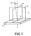
- FIG. 1 a twisted nematic liquid crystal cell 1 with two vision planes, the horizontal plane 2 and the vertical plane 3.
- a voltage across the electrodes creates an electric field across the liquid crystal straightening the direction of the molecules, and the pixel is in the non-conducting state, ie black.
- the angular distribution of the transmittance of light is symmetrical in the horizontal plane 2, and asymmetrical in the vertical plane 3.
- the direction of maximum contrast D corresponding to the minimum transmittance, is located in the vertical plane 3, its orientation depending on the voltage applied between the electrodes of the pixel, ie the brightness.
- the image displayed by the screen degrades as a function of the viewing angle at which it is perceived, this being able to go as far as an inversion of contrast for large angles.
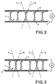
- FIG. 2 represents the alignment of these molecules 4 in the case of a nematic liquid crystal twisted in the presence of a voltage U between the electrodes 5 and 6.
- a alignment layer 7 which may be polyimide
- the directions of the dark 8 and light 9 zones mentioned above are given by the inclination that the molecules take in the presence of the electric field.
- the problem with this solution is its difficult technological realization, requiring etching of two different layers of alignment of the liquid crystal molecules, which appears extremely difficult to achieve in mass production.
- the present invention overcomes these drawbacks thanks to a screen structure which is very simple to produce.
- the present invention relates to an electrooptical cell (pixel) formed of two substrate plates comprising one, a pixel electrode and the other, a counter electrode between which liquid crystal molecules are included, in which the counter electrode is divided into two parts (or domains) by a groove, this groove preferably cutting the pixel in the middle, characterized in that a non-zero bias voltage is applied between the electrode and the counter-electrode when the pixel is not addressed.
- this voltage is between 0.8 and 1.3 times the value of the threshold polarization voltage of the liquid crystal in the presence of a homogeneous electric field.
- said cell has alignment layers of homogeneous liquid crystal molecules, the division of each pixel into two domains made up of molecules having different inclinations being only caused by the effect of the electric field between said electrode pixel and said counter electrode.
- said alignment layer can impose on the molecules of the liquid crystal either, an alignment strictly parallel to the stratum, or, in the presence of a intrinsic pre-tilt of said alignment layer, an anti-parallel alignment.
- Another improvement of the present invention consists in slightly increasing the thickness of the liquid crystal so as to maintain the optical characteristic in the presence of said bias voltage when the pixel is not addressed.
- this thickness is such that its product with birefringence, divided by the wavelength of light, is slightly greater than the constant ⁇ 3/2, typically between 1.1 and 1.5 times this constant.
- Another characteristic of the present invention is that an opaque material is deposited on one of the substrate plates in order to mask the groove of the counter electrode, this opaque material being able to be used as storage capacity.
- the present invention also relates to a liquid crystal screen comprising such electrooptical cells.
- the alignment layers 7 can be treated so as to obtain liquid crystal molecules 4, the alignment of which is said to be parallel, that is to say that they have a pre-inclination of 0 °. .
- This can be achieved by light brushing or printing the polyimide, or by oblique deposition of silicon oxide SiO.
- it is possible to use a so-called antiparallel alignment by using an alignment layer creating a pre-tilt other than zero. In this case, the layers at the top and bottom of the cell are arranged so that the two pre-slopes are opposite and cancel each other out. This type of alignment is called anti-parallel alignment.
- FIG. 5 is shown the section of a liquid crystal screen usable in the invention. It consists of two transparent substrate plates 11 on the inner surfaces of which are deposited transparent electrodes 14 and a transparent counter electrode 15. On the inner faces of these electrodes 14 and 15 are deposited and treated alignment layers 13. These layers can be either of the type allowing parallel alignment, or of the type imposing a pre-tilt of the liquid crystal molecules 4 located between these two layers. In the latter case, said layers at the top and bottom of the cell are arranged in an anti-parallel manner. Said liquid crystal can be twisted nematic or of any other type whose electrooptic effects are modified by an electric field E. Furthermore, these pixels are surrounded by two polarizers 7.
- the counter electrode 15 has a groove 18 cutting the pixel in the middle.
- this groove has a width of 0.5 to 2 times the thickness of the layer of the liquid crystal molecules 4, which is typically between 3 and 10 ⁇ m.
- a potential difference U is applied to the pixel electrodes 14 and to the counter electrode 15, this groove creates a component lateral to the electric field E.
- the electric field E is then perpendicular to the electrodes in the areas where they are made face, and oblique in the areas at the edges of the pixel electrodes 14 and in the areas between the groove 18 and the electrode 14, as indicated in FIG. 5.
- two optical domains each having different tilt directions are created by the non-homogeneous distribution of the electric field E due to the pixel structure according to the invention.
- an opaque material 16 for example on the outer face of the electrode 14.
- This material can be metal and can be used as storage capacity, for example in the case of addressing of active matrix.
- the counter electrode In the case of a screen addressed by an active matrix, the counter electrode generally covers the entire screen. In this case, it is necessary to etch this counter electrode in order to produce the grooves 18 in a very simple additional step.
- the mask used for this step can be the same as that used to deposit the opaque mask 16.
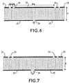
- FIG. 6 represents a sectional view of a liquid crystal screen according to a first embodiment of the invention. It is formed by electrodes 21, 22 and 23 separated by selection (or data) lines 24, and by a counter electrode 25 provided with grooves 26.
- the liquid crystal molecules 4 have a parallel alignment as described on the Figure 4a.
- Figure 7 shows a screen structure identical to that of the previous figure but with a pre-tilt of 1 °, the liquid crystal molecules have an anti-parallel alignment as described in Figure 4b.
- the polarization is not equal to zero when the pixel is not addressed (OFF state), so as to maintain the structure of the domains.
- the value of the bias voltage U is between 0.8 and 1.3 times the value of the threshold voltage of the liquid crystal in the presence of a homogeneous field.
- ⁇ n the birefringence
- ⁇ the wavelength of light.
- the present invention applies to all types of liquid crystal screens, direct vision or projection, provided with integrated or non-integrated control circuits.
Abstract
Description
La présente invention concerne une structure particulière de cellule électrooptique (ou pixel) d'écrans à cristaux liquides permettant une amélioration de la caractéristique angulaire par rapport aux écrans à cristaux liquides connus.The present invention relates to a particular electrooptical cell (or pixel) structure of liquid crystal screens allowing an improvement in the angular characteristic compared to known liquid crystal screens.
Les écrans à cristaux liquides à vision directe ou à projection sont en général composés de lignes (lignes de sélection) et colonnes (lignes de données) aux intersections desquelles sont situées les électrodes de pixels connectées au travers de transistors à ces lignes. Les grilles de ces transistors forment les lignes de sélection et sont commandées par des circuits de commande périphériques qui balayent les lignes et rendent passants les transistors de chaque ligne en permettant, par les lignes de données connectées aux autres circuits de commande périphériques, de polariser les électrodes et modifier les propriétés optiques du cristal liquide compris entre ces électrodes et la contre-électrode (ou électrode de référence), permettant ainsi la formation d'images sur l'écran.Direct vision or projection liquid crystal screens are generally composed of lines (selection lines) and columns (data lines) at the intersections of which are located the pixel electrodes connected through transistors to these lines. The gates of these transistors form the selection lines and are controlled by peripheral control circuits which scan the lines and make the transistors of each line pass by, by means of the data lines connected to the other peripheral control circuits, to polarize the electrodes and modify the optical properties of the liquid crystal between these electrodes and the counter electrode (or reference electrode), thus allowing the formation of images on the screen.
Un des inconvénients majeurs de ce type d'écran est que les propriétés optiques dépendent de la vision angulaire que l'on en a, c'est à dire qu'elles dépendent de la direction de propagation de la lumière au travers des pixels, en particulier pour les images comportant différents niveaux de gris. Sur la figure 1 est représentée une cellule à cristaux liquides nématiques twistés 1 avec deux plans de vision, le plan horizontal 2 et le plan vertical 3. Dans le cas de polariseurs croisés, une tension aux bornes des électrodes crée un champ électrique au travers du cristal liquide redressant la direction des molécules, et le pixel est dans l'état non passant, c'est à dire noir. La distribution angulaire de la transmitance de la lumière est symétrique dans le plan horizontal 2, et assymétrique dans le plan vertical 3. De ce fait, il existe une zone sombre S et une zone claire C de part et d'autre du plan horizontal. La direction de contraste maximum D, correspondant à la transmitance minimum, est située dans le plan vertical 3, son orientation dépendant de la tension appliquée entre les électrodes du pixel, c'est à dire de la luminosité. Ainsi, l'image affichée par l'écran se dégrade en fonction de l'angle de vision selon laquelle elle est perçue, cela pouvant aller jusqu'à une inversion de contraste pour de grands angles.One of the major drawbacks of this type of screen is that the optical properties depend on the angular vision that one has, that is to say that they depend on the direction of propagation of light through the pixels, in especially for images with different gray levels. In FIG. 1 is shown a twisted nematic liquid crystal cell 1 with two vision planes, the
La direction des différentes zones de vision dépend de l'orientation des molécules du cristal liquide. La figure 2 représente l'alignement de ces molécules 4 dans le cas d'un cristal liquide nématique twisté en présence d'une tension U entre les électrodes 5 et 6. Ces électrodes sont recouvertes sur leurs parties faisant face au cristal liquide d'une couche d'alignement 7 (qui peut être du polyimide) imposant une direction particulière aux molécules 4 du cristal liquide. Les directions des zones sombre 8 et claire 9 évoquées plus haut sont données par l'inclinaison que prennent les molécules en présence du champ électrique. En traitant d'une certaine manière le revêtement de polyimide, on peut imposer aux molécules du cristal liquide une préinclinaison, à savoir un angle entre les molécules les plus proches du substrat et le substrat lui même en l'absence de champ électrique.The direction of the different vision zones depends on the orientation of the molecules of the liquid crystal. FIG. 2 represents the alignment of these molecules 4 in the case of a nematic liquid crystal twisted in the presence of a voltage U between the
Afin de palier à ces inconvénients et obtenir une meilleure vision angulaire, un article de K.H. YANG "11th International Display Research Conference", 1991, page 68, propose une solution illustrée par la figure 3 et qui consiste à diviser chaque pixel en deux domaines ayant chacun une inclinaison opposée lorsqu'une tension U est appliquée aux électrodes. Les couches d'alignement de chacune des moitiés des pixels sont gravées de manière à créer des tilts opposés, cela peut être obtenu par deux étapes, séparées par une étape de masquage, de frottements antiparallèles de ces couches d'alignement en polyimide, ou bien de dépôt à vide d'oxyde de Silicium SiO. Dans ce cas, les effets se neutralisent et on obtient une vision symétrique quel que soit le plan de vision.In order to overcome these drawbacks and obtain a better angular vision, an article by KH YANG "11th International Display Research Conference", 1991, page 68, proposes a solution illustrated by FIG. 3 and which consists in dividing each pixel into two domains having each an opposite inclination when a voltage U is applied to the electrodes. The alignment layers of each of the halves of the pixels are etched so as to create opposite tilts, this can be obtained by two steps, separated by a masking step, from antiparallel friction of these polyimide alignment layers, or else of vacuum deposition of silicon oxide SiO. In this case, the effects are neutralized and a symmetrical vision is obtained whatever the plane of vision.
Le problème de cette solution est sa réalisation technologique difficile, nécessitant une gravure de deux couches différentes d'alignement des molécules de cristal liquide, ce qui apparait extrèmement difficile à réaliser en production de masse. La présente invention permet de résoudre ces inconvénients grâce à une structure d'écran très simple à réaliser.The problem with this solution is its difficult technological realization, requiring etching of two different layers of alignment of the liquid crystal molecules, which appears extremely difficult to achieve in mass production. The present invention overcomes these drawbacks thanks to a screen structure which is very simple to produce.
En effet, la présente invention concerne une cellule électrooptique (pixel) formée de deux plaques substrats comportant l'une, une électrode de pixel et l'autre, une contre-électrode entre lesquels sont comprises des molécules de cristal liquide, dans laquelle la contre électrode est divisée en deux parties (ou domaines) par une rainure, cette rainure coupant de préférence le pixel en son milieu, caractérisé en ce qu'une tension de polarisation non nulle est appliquée entre l'électrode et la contre-électrode lorsque le pixel n'est pas adressé. De préférence, cette tension est comprise entre 0,8 et 1,3 fois la valeur de la tension de polarisation de seuil du cristal liquide en présence d'un champ électrique homogène.In fact, the present invention relates to an electrooptical cell (pixel) formed of two substrate plates comprising one, a pixel electrode and the other, a counter electrode between which liquid crystal molecules are included, in which the counter electrode is divided into two parts (or domains) by a groove, this groove preferably cutting the pixel in the middle, characterized in that a non-zero bias voltage is applied between the electrode and the counter-electrode when the pixel is not addressed. Preferably, this voltage is between 0.8 and 1.3 times the value of the threshold polarization voltage of the liquid crystal in the presence of a homogeneous electric field.
Une autre caractéristique de la présente invention est que ladite cellule a des couches d'alignement de molécules de cristal liquide homogènes, la division de chaque pixel en deux domaines constitués de molécules ayant des inclinaisons différentes étant uniquement provoquée par effet du champ électrique entre ladite électrode de pixel et ladite contre-électrode.Another characteristic of the present invention is that said cell has alignment layers of homogeneous liquid crystal molecules, the division of each pixel into two domains made up of molecules having different inclinations being only caused by the effect of the electric field between said electrode pixel and said counter electrode.
Afin d'éviter une préférence pour un des deux domaines introduit par la couche d'alignement, ladite couche d'alignement peut imposer aux molécules du cristal liquide soit, un alignement strictement parallèle à la strate, soit, en cas de présence d'une pré-inclinaison intrinsèque de ladite couche d'alignement, un alignement anti-parallèle.In order to avoid a preference for one of the two fields introduced by the alignment layer, said alignment layer can impose on the molecules of the liquid crystal either, an alignment strictly parallel to the stratum, or, in the presence of a intrinsic pre-tilt of said alignment layer, an anti-parallel alignment.
Un autre perfectionnement de la présente invention consiste à augmenter légèrement l'épaisseur du cristal liquide de manière à maintenir la caractéristique optique en présence de ladite tension de polarisation lorsque le pixel n'est pas adressé. De préférence cette épaisseur est telle que son produit avec la biréfringence, divisé par la longueur d'onde de la lumière, soit légèrement supérieur à la constante √ 3 / 2, typiquement compris entre 1,1 et 1,5 fois cette constante.Another improvement of the present invention consists in slightly increasing the thickness of the liquid crystal so as to maintain the optical characteristic in the presence of said bias voltage when the pixel is not addressed. Preferably this thickness is such that its product with birefringence, divided by the wavelength of light, is slightly greater than the constant √ 3/2, typically between 1.1 and 1.5 times this constant.
Une autre caractéristique de la présente invention est qu'un matériau opaque est déposé sur l'une des plaques substrats afin de masquer la rainure de la contre électrode, ce matériau opaque pouvant être utilisé comme capacité de stockage.Another characteristic of the present invention is that an opaque material is deposited on one of the substrate plates in order to mask the groove of the counter electrode, this opaque material being able to be used as storage capacity.
D'autre part la présente invention concerne aussi un écran à cristaux liquides comportant de telles cellules électrooptiques.On the other hand the present invention also relates to a liquid crystal screen comprising such electrooptical cells.
La présente invention sera mieux comprise et des avantages supplémentaires apparaitront à la lecture de la description qui va suivre illustrée par les figures suivantes:
- . la figure 1 déjà décrite représente un exemple de pixel constitué d'un cristal liquide nématique twisté selon l'art antérieur et montre la présence de deux zones sombre et claire,
- . la figure 2 déjà décrite représente une vue en coupe du même pixel pour illustrer les orientations de ces zones,
- . la figure 3 déjà décrite représente une solution proposée par l'art antérieur pour annihiler l'effet néfaste de ces zones,
- . les figures 4a et 4b représentent des molécules de cristal liquide nématique twisté ayant respectivement en l'absence de champ électrique un alignement parallèle et antiparallèle qui sont utilisés dans la présente invention,
- . la figure 5 représente un mode de réalisation préférentiel d'une cellule à laquelle s'applique la présente invention,
- . et les figures 6a et 6b représentent les orientations obtenues en utilisant une structure de pixel selon deux modes de réalisation de l'invention.
- . FIG. 1, already described, represents an example of a pixel consisting of a nematic liquid crystal twisted according to the prior art and shows the presence of two dark and light areas,
- . FIG. 2 already described represents a sectional view of the same pixel to illustrate the orientations of these zones,
- . FIG. 3, already described, represents a solution proposed by the prior art for eliminating the harmful effect of these areas,
- . FIGS. 4a and 4b represent molecules of twisted nematic liquid crystal having respectively in the absence of an electric field a parallel and antiparallel alignment which are used in the present invention,
- . FIG. 5 represents a preferred embodiment of a cell to which the present invention applies,
- . and FIGS. 6a and 6b represent the orientations obtained using a pixel structure according to two embodiments of the invention.
Une des caractéristiques de la présente invention est l'utilisation d'un alignement des molécules de cristal liquide sans pré-inclinaison effective en l'absence d'un champ électrique. Comme cela est illustré par la figure 4a, les couches d'alignement 7 peuvent être traitées de manière à obtenir des molécules de cristal liquide 4 dont l'alignement est dit parallèle, c'est à dire qu'elles ont une préinclinaison de 0°. Cela peut être obtenu par léger brossage ou impression du polyimide, ou bien par dépôt oblique d'oxyde de Silicium SiO. Alternativement, il est possible d'utiliser un alignement dit antiparallèle en utilisant une couche d'alignement créant une préinclinaison différente de zéro. Dans ce cas, les couches en haut et en bas de la cellule sont arrangées de façon à ce que les deux pré-inclinaisons soient opposées et s'annulent. Ce type d'alignement est appelé alignement anti-parallèle.One of the characteristics of the present invention is the use of an alignment of the liquid crystal molecules without effective pre-tilt in the absence of an electric field. As illustrated in FIG. 4a, the
Sur la figure 5 est représentée la section d'un écran à cristaux liquides utilisable dans l'invention. Il est constitué de par deux plaques substrats transparents 11 sur les surfaces intérieures desquels sont déposées des électrodes transparentes 14 et une contre électrode transparente 15. Sur les faces intérieures de ces électrodes 14 et 15 sont déposées et traitées des couches d'alignement 13. Ces couches peuvent être, soit du type permettant un alignement parallèle, soit du type imposant une pré-inclinaison des molécules de cristal liquides 4 situées entre ces deux couches. Dans ce dernier cas, lesdites couches en haut et en bas de la cellule sont arrangées de façon anti-parallèle. Ledit cristal liquide peut être nématique twisté ou d'un tout autre type dont les effets électrooptiques sont modifiés par un champ électrique E. Par ailleurs, ces pixels sont encadrés par deux polariseurs 7.In Figure 5 is shown the section of a liquid crystal screen usable in the invention. It consists of two
La contre électrode 15 comporte une rainure 18 coupant le pixel en son milieu. De préférence cette rainure a une largeur de 0.5 à 2 fois l'épaisseur de la couche des molécules de cristal liquide 4, qui est typiquement entre 3 et 10 µm. Lorsqu'une différence de potentiel U est appliquée aux électrodes de pixel 14 et à la contre électrode 15, cette rainure crée une composante latérale au champ électrique E. Le champ électrique E est alors perpendiculaire aux électrodes dans les zones où celles-ci se font face, et oblique dans les zones aux bords des électrodes de pixel 14 et dans les zones comprises entre la rainure 18 et l'électrode 14, comme cela est indiqué sur la figure 5. Ainsi, deux domaines optiques ayant chacun des directions de tilt différentes sont créés par la distribution non homogène du champ électrique E due à la structure de pixel selon l'invention.The counter electrode 15 has a
Afin d'éliminer les perturbations optiques dues à la frontière entre les deux domaines, il est nécessaire de masquer la partie autour de la rainure 18 par le dépôt d'un matériau opaque 16, par exemple sur la face extérieure de l'électrode 14. Ce matériau peut être du métal et peut être utilisé comme capacité de stockage, par exemple dans le cas d'un adressage de matrice active.In order to eliminate the optical disturbances due to the border between the two domains, it is necessary to mask the part around the
Dans le cas d'un écran adressé par une matrice active, la contre électrode recouvre en général tout l'écran. Dans ce cas, il est nécessaire de graver cette contre électrode afin de réaliser les rainures 18 dans une étape supplémentaire très simple. Le masque utilisé pour cette étape peut être le même que celui utilisé pour déposer le masque opaque 16.In the case of a screen addressed by an active matrix, the counter electrode generally covers the entire screen. In this case, it is necessary to etch this counter electrode in order to produce the
Il est bien évident que cet adressage particulier n'est pas limitatif.It is obvious that this particular addressing is not limiting.
La figure 6 représente une vue en coupe d'un écran à cristaux liquides selon un premier mode de réalisation de l'invention. Il est formé d'électrodes 21, 22 et 23 séparées par des lignes de sélection (ou de données) 24, et d'une contre électrode 25 munie de rainures 26. Les molécules de cristal liquide 4 ont un alignement parallèle comme décrit sur la figure 4a.FIG. 6 represents a sectional view of a liquid crystal screen according to a first embodiment of the invention. It is formed by
La figure 7 représente quant à elle une structure d'écran identique à celle de la figure précédente mais avec une préinclinaison de 1°, les molécules de cristal liquide ont un alignement anti parallèle comme décrit sur la figure 4b.Figure 7 shows a screen structure identical to that of the previous figure but with a pre-tilt of 1 °, the liquid crystal molecules have an anti-parallel alignment as described in Figure 4b.
Du fait du temps de formation relativement long des deux domaines, conformément à la présente invention, la polarisation n'est pas égale à zéro lorsque le pixel n'est pas adressé (état OFF), de manière à maintenir la structure des domaines. De préférence, la valeur de la tension de polarisation U est comprise entre 0,8 et 1,3 fois la valeur de la tension de seuil du cristal liquide en présence d'un champ homogène.Due to the relatively long formation time of the two domains, in accordance with the present invention, the polarization is not equal to zero when the pixel is not addressed (OFF state), so as to maintain the structure of the domains. Preferably, the value of the bias voltage U is between 0.8 and 1.3 times the value of the threshold voltage of the liquid crystal in the presence of a homogeneous field.
D'autre part, afin de préserver les propriétés optiques de l'écran, il est préférable de modifier légèrement l'épaisseur du volume de cristal liquide. En effet, cette épaisseur d est en général choisie de manière à ce que la biréfringence effective donne le maximum de transmission dans l'état OFF ainsi que de bonnes caractéristiques angulaires. C'est à dire qu'il faut que le produit dΔn/λ = √3/2 ait une certaine valeur, Δn étant la biréfringence et λ la longueur d'onde de la lumière. Dans le cas d'une prépolarisation dans l'état OFF, les molécules de cristal liquide étant légèrement inclinées, la valeur effective de d.Δn est légèrement diminuée. Ainsi, il est préférable d'augmenter l'épaisseur du cristal liquide afin de compenser cet effet. Une telle modification est préférable toutes les fois où cette valeur d.Δn intervient.On the other hand, in order to preserve the optical properties of the screen, it is preferable to slightly modify the thickness of the volume of liquid crystal. In fact, this thickness d is generally chosen so that the effective birefringence gives the maximum transmission in the OFF state as well as good angular characteristics. That is, the product dΔn / λ = √3 / 2 must have a certain value, Δn being the birefringence and λ the wavelength of light. In the case of a prepolarization in the OFF state, the liquid crystal molecules being slightly inclined, the effective value of d.Δn is slightly reduced. Thus, it is preferable to increase the thickness of the liquid crystal in order to compensate for this effect. Such a modification is preferable whenever this value d.Δn occurs.
La présente invention s'applique à tous les types d'écrans à cristaux liquides, à vision directe ou à projection, munis de circuits de commande intégrés ou non.The present invention applies to all types of liquid crystal screens, direct vision or projection, provided with integrated or non-integrated control circuits.
Claims (10)
Applications Claiming Priority (2)
| Application Number | Priority Date | Filing Date | Title |
|---|---|---|---|
| FR9502776A FR2731526B1 (en) | 1995-03-09 | 1995-03-09 | LIQUID CRYSTAL SCREEN WITH IMPROVED ANGLE OF VIEW |
| FR9502776 | 1995-03-09 |
Publications (2)
| Publication Number | Publication Date |
|---|---|
| EP0731374A1 true EP0731374A1 (en) | 1996-09-11 |
| EP0731374B1 EP0731374B1 (en) | 2010-04-14 |
Family
ID=9476908
Family Applications (1)
| Application Number | Title | Priority Date | Filing Date |
|---|---|---|---|
| EP96400396A Expired - Lifetime EP0731374B1 (en) | 1995-03-09 | 1996-02-26 | Liquid crystal display with improved viewing angle |
Country Status (5)
| Country | Link |
|---|---|
| US (1) | US6327014B1 (en) |
| EP (1) | EP0731374B1 (en) |
| JP (1) | JPH08292414A (en) |
| DE (1) | DE69638160D1 (en) |
| FR (1) | FR2731526B1 (en) |
Cited By (1)
| Publication number | Priority date | Publication date | Assignee | Title |
|---|---|---|---|---|
| EP1734400A1 (en) * | 1998-11-27 | 2006-12-20 | SANYO ELECTRIC Co., Ltd. | Liquid crystal display device |
Families Citing this family (5)
| Publication number | Priority date | Publication date | Assignee | Title |
|---|---|---|---|---|
| JP3966614B2 (en) * | 1997-05-29 | 2007-08-29 | 三星電子株式会社 | Wide viewing angle LCD |
| US8913000B2 (en) * | 2007-06-15 | 2014-12-16 | Ricoh Co., Ltd. | Video playback on electronic paper displays |
| CN102736325B (en) * | 2011-03-31 | 2015-08-12 | 京东方科技集团股份有限公司 | A kind of dot structure and manufacture method, display device |
| CN105676549B (en) * | 2016-04-14 | 2018-12-21 | 京东方科技集团股份有限公司 | Display panel and preparation method thereof and display device |
| CN105759528B (en) | 2016-05-19 | 2019-01-18 | 京东方科技集团股份有限公司 | Display panel assembly, display device and its driving method |
Citations (3)
| Publication number | Priority date | Publication date | Assignee | Title |
|---|---|---|---|---|
| EP0445777A2 (en) * | 1990-03-08 | 1991-09-11 | Stanley Electric Co., Ltd. | Liquid crystal display device |
| US5309264A (en) * | 1992-04-30 | 1994-05-03 | International Business Machines Corporation | Liquid crystal displays having multi-domain cells |
| EP0636917A1 (en) * | 1993-07-27 | 1995-02-01 | Sharp Kabushiki Kaisha | Liquid crystal display |
Family Cites Families (7)
| Publication number | Priority date | Publication date | Assignee | Title |
|---|---|---|---|---|
| JPS6045219A (en) * | 1983-08-23 | 1985-03-11 | Toshiba Corp | Active matrix type display device |
| JP2523811B2 (en) * | 1988-09-02 | 1996-08-14 | 株式会社日立製作所 | Liquid crystal light modulator |
| JPH0642125B2 (en) * | 1988-10-04 | 1994-06-01 | シャープ株式会社 | Projection equipment |
| US5084778A (en) * | 1989-12-26 | 1992-01-28 | General Electric Company | Electrode structure for removing field-induced disclination lines in a phase control type of liquid crystal device |
| JPH0786622B2 (en) * | 1990-11-02 | 1995-09-20 | スタンレー電気株式会社 | Liquid crystal display |
| JPH06194687A (en) * | 1992-10-30 | 1994-07-15 | Nec Corp | Transmission type active matrix liquid crystal element |
| JP2924506B2 (en) * | 1992-10-27 | 1999-07-26 | 日本電気株式会社 | Pixel structure of active matrix liquid crystal display |
-
1995
- 1995-03-09 FR FR9502776A patent/FR2731526B1/en not_active Expired - Fee Related
-
1996
- 1996-02-26 DE DE69638160T patent/DE69638160D1/en not_active Expired - Lifetime
- 1996-02-26 EP EP96400396A patent/EP0731374B1/en not_active Expired - Lifetime
- 1996-02-28 US US08/608,042 patent/US6327014B1/en not_active Expired - Lifetime
- 1996-03-08 JP JP8079372A patent/JPH08292414A/en active Pending
Patent Citations (3)
| Publication number | Priority date | Publication date | Assignee | Title |
|---|---|---|---|---|
| EP0445777A2 (en) * | 1990-03-08 | 1991-09-11 | Stanley Electric Co., Ltd. | Liquid crystal display device |
| US5309264A (en) * | 1992-04-30 | 1994-05-03 | International Business Machines Corporation | Liquid crystal displays having multi-domain cells |
| EP0636917A1 (en) * | 1993-07-27 | 1995-02-01 | Sharp Kabushiki Kaisha | Liquid crystal display |
Non-Patent Citations (3)
| Title |
|---|
| KOIKE Y ET AL: "A Full-Color TFT-LCD with a Domain Divided Twisted Nematic Structure", SID INTERNATIONAL SYMPOSIUM DIGEST OF PAPERS, BOSTON, MAY 17 - 22, 1992, vol. 23, 17 May 1992 (1992-05-17), SOCIETY FOR INFORMATION DISPLAY, pages 798 - 801, XP000479122 * |
| LIEN A ET AL: "TFT-Addressed Two-Domain TN VGA Displays Fabricated Using the Parallel Fringe Field Method", SID INTERNATIONAL SYMPOSIUM - DIGEST OF TECHNICAL PAPERS, S.JOSE, JUNE 14 - 16, 1994, vol. 25, 14 June 1994 (1994-06-14), SOCIETY FOR INFORMATION DISPLAY, pages 594 - 596, XP000462734 * |
| LIEN A ET AL: "Two-Domain TN-LCDs Fabricated by Parallel Fringe Field Method", SID INTERNATIONAL SYMPOSIUM - DIGEST OF TECHNICAL PAPERS, SEATTLE, MAY 16 - 21, 1993, vol. 24 PART 1, 16 May 1993 (1993-05-16), SOCIETY FOR INFORMATION DISPLAY, pages 269 - 272, XP000508249 * |
Cited By (2)
| Publication number | Priority date | Publication date | Assignee | Title |
|---|---|---|---|---|
| EP1734400A1 (en) * | 1998-11-27 | 2006-12-20 | SANYO ELECTRIC Co., Ltd. | Liquid crystal display device |
| US7295273B2 (en) | 1998-11-27 | 2007-11-13 | Sanyo Electric Co., Ltd. | Liquid crystal display device having particular drain lines and orientation control window |
Also Published As
| Publication number | Publication date |
|---|---|
| FR2731526A1 (en) | 1996-09-13 |
| US6327014B1 (en) | 2001-12-04 |
| DE69638160D1 (en) | 2010-05-27 |
| JPH08292414A (en) | 1996-11-05 |
| EP0731374B1 (en) | 2010-04-14 |
| FR2731526B1 (en) | 1997-04-04 |
Similar Documents
| Publication | Publication Date | Title |
|---|---|---|
| FR2765697A1 (en) | PROCESS FOR PRODUCING TWO DOMAINS WITHIN A LIQUID CRYSTAL LAYER | |
| FR2760542A1 (en) | Closed cavity liquid crystal cell | |
| EP2366125B1 (en) | Optical element with variable optical power | |
| FR2764087A1 (en) | LIQUID CRYSTAL DISPLAY DEVICE | |
| FR2545961A1 (en) | FRAME SEQUENCE COLOR DISPLAY SYSTEM AND METHOD OF USING LIQUID CRYSTAL CELL FOR SUCH A SYSTEM | |
| FR2773225A1 (en) | LIQUID CRYSTAL DISPLAY DEVICE AND METHOD FOR MANUFACTURING THE SAME | |
| EP0058593B1 (en) | Matrix display device with several sets of electrodes and addressing method therefor | |
| EP2721598A1 (en) | Liquid crystal display comprising erase electrodes | |
| EP0929839A1 (en) | Display screen with active matrix | |
| FR2787205A1 (en) | MULTI-DOMAIN LIQUID CRYSTAL DISPLAY DEVICE | |
| EP1101149B1 (en) | Improving the angle of view of a lcd screen by novel birefringent film stacking | |
| EP0731374B1 (en) | Liquid crystal display with improved viewing angle | |
| EP1430357B1 (en) | Bistable nematic liquid crystal display device with improved optical mask | |
| FR2803940A1 (en) | MULTI-DOMAIN LIQUID CRYSTAL DISPLAY DEVICE | |
| EP0792474B1 (en) | Liquid crystal display device using birefringent films | |
| EP0209439B1 (en) | Electro-optical display device with liquid crystals | |
| FR2578994A1 (en) | Ferroelectric liquid crystal display device | |
| EP4198623A1 (en) | Liquid crystal phase modulation device | |
| FR2550368A1 (en) | LIQUID CRYSTAL DISPLAY DEVICE WITH SCREEN PROTECTION FOR ELECTRODES | |
| EP0432255B1 (en) | Birefringent optical translator and birefringent three-dimensional screen | |
| FR2546324A1 (en) | Visual display device with memory held on | |
| JPS63228124A (en) | Liquid crystal electrooptic device | |
| FR2789186A1 (en) | Liquid crystal screen device with wider horizontal viewing angle, comprising additional optical layers made of biaxial birefringent and uniaxial positive materials | |
| JPH10260428A (en) | Method and element for phase spatial optical modulation | |
| JP2005062901A (en) | Liquid crystal display element and optically anisotropic element |
Legal Events
| Date | Code | Title | Description |
|---|---|---|---|
| PUAI | Public reference made under article 153(3) epc to a published international application that has entered the european phase |
Free format text: ORIGINAL CODE: 0009012 |
|
| AK | Designated contracting states |
Kind code of ref document: A1 Designated state(s): DE FR GB NL |
|
| 17P | Request for examination filed |
Effective date: 19960820 |
|
| RAP1 | Party data changed (applicant data changed or rights of an application transferred) |
Owner name: THOMSON MULTIMEDIA |
|
| 17Q | First examination report despatched |
Effective date: 20040308 |
|
| GRAP | Despatch of communication of intention to grant a patent |
Free format text: ORIGINAL CODE: EPIDOSNIGR1 |
|
| GRAS | Grant fee paid |
Free format text: ORIGINAL CODE: EPIDOSNIGR3 |
|
| GRAA | (expected) grant |
Free format text: ORIGINAL CODE: 0009210 |
|
| AK | Designated contracting states |
Kind code of ref document: B1 Designated state(s): DE FR GB NL |
|
| REG | Reference to a national code |
Ref country code: GB Ref legal event code: FG4D Free format text: NOT ENGLISH |
|
| REF | Corresponds to: |
Ref document number: 69638160 Country of ref document: DE Date of ref document: 20100527 Kind code of ref document: P |
|
| REG | Reference to a national code |
Ref country code: NL Ref legal event code: VDEP Effective date: 20100414 |
|
| PG25 | Lapsed in a contracting state [announced via postgrant information from national office to epo] |
Ref country code: NL Free format text: LAPSE BECAUSE OF FAILURE TO SUBMIT A TRANSLATION OF THE DESCRIPTION OR TO PAY THE FEE WITHIN THE PRESCRIBED TIME-LIMIT Effective date: 20100414 |
|
| PLBE | No opposition filed within time limit |
Free format text: ORIGINAL CODE: 0009261 |
|
| STAA | Information on the status of an ep patent application or granted ep patent |
Free format text: STATUS: NO OPPOSITION FILED WITHIN TIME LIMIT |
|
| 26N | No opposition filed |
Effective date: 20110117 |
|
| REG | Reference to a national code |
Ref country code: FR Ref legal event code: PLFP Year of fee payment: 20 |
|
| PGFP | Annual fee paid to national office [announced via postgrant information from national office to epo] |
Ref country code: DE Payment date: 20150219 Year of fee payment: 20 |
|
| PGFP | Annual fee paid to national office [announced via postgrant information from national office to epo] |
Ref country code: FR Payment date: 20150220 Year of fee payment: 20 Ref country code: GB Payment date: 20150223 Year of fee payment: 20 |
|
| REG | Reference to a national code |
Ref country code: DE Ref legal event code: R071 Ref document number: 69638160 Country of ref document: DE |
|
| REG | Reference to a national code |
Ref country code: GB Ref legal event code: PE20 Expiry date: 20160225 |
|
| PG25 | Lapsed in a contracting state [announced via postgrant information from national office to epo] |
Ref country code: GB Free format text: LAPSE BECAUSE OF EXPIRATION OF PROTECTION Effective date: 20160225 |