EP0729184A2 - Semiconductor package stack module and method of producing the same - Google Patents
Semiconductor package stack module and method of producing the same Download PDFInfo
- Publication number
- EP0729184A2 EP0729184A2 EP96102773A EP96102773A EP0729184A2 EP 0729184 A2 EP0729184 A2 EP 0729184A2 EP 96102773 A EP96102773 A EP 96102773A EP 96102773 A EP96102773 A EP 96102773A EP 0729184 A2 EP0729184 A2 EP 0729184A2
- Authority
- EP
- European Patent Office
- Prior art keywords
- carrier
- semiconductor package
- module
- lsi chip
- carriers
- Prior art date
- Legal status (The legal status is an assumption and is not a legal conclusion. Google has not performed a legal analysis and makes no representation as to the accuracy of the status listed.)
- Withdrawn
Links
Images


Classifications
-
- H—ELECTRICITY
- H01—ELECTRIC ELEMENTS
- H01L—SEMICONDUCTOR DEVICES NOT COVERED BY CLASS H10
- H01L24/00—Arrangements for connecting or disconnecting semiconductor or solid-state bodies; Methods or apparatus related thereto
- H01L24/01—Means for bonding being attached to, or being formed on, the surface to be connected, e.g. chip-to-package, die-attach, "first-level" interconnects; Manufacturing methods related thereto
- H01L24/26—Layer connectors, e.g. plate connectors, solder or adhesive layers; Manufacturing methods related thereto
- H01L24/28—Structure, shape, material or disposition of the layer connectors prior to the connecting process
-
- H—ELECTRICITY
- H01—ELECTRIC ELEMENTS
- H01L—SEMICONDUCTOR DEVICES NOT COVERED BY CLASS H10
- H01L21/00—Processes or apparatus adapted for the manufacture or treatment of semiconductor or solid state devices or of parts thereof
- H01L21/02—Manufacture or treatment of semiconductor devices or of parts thereof
- H01L21/04—Manufacture or treatment of semiconductor devices or of parts thereof the devices having at least one potential-jump barrier or surface barrier, e.g. PN junction, depletion layer or carrier concentration layer
- H01L21/50—Assembly of semiconductor devices using processes or apparatus not provided for in a single one of the subgroups H01L21/06 - H01L21/326, e.g. sealing of a cap to a base of a container
- H01L21/56—Encapsulations, e.g. encapsulation layers, coatings
- H01L21/563—Encapsulation of active face of flip-chip device, e.g. underfilling or underencapsulation of flip-chip, encapsulation preform on chip or mounting substrate
-
- H—ELECTRICITY
- H01—ELECTRIC ELEMENTS
- H01L—SEMICONDUCTOR DEVICES NOT COVERED BY CLASS H10
- H01L25/00—Assemblies consisting of a plurality of individual semiconductor or other solid state devices ; Multistep manufacturing processes thereof
- H01L25/03—Assemblies consisting of a plurality of individual semiconductor or other solid state devices ; Multistep manufacturing processes thereof all the devices being of a type provided for in the same subgroup of groups H01L27/00 - H01L33/00, or in a single subclass of H10K, H10N, e.g. assemblies of rectifier diodes
- H01L25/10—Assemblies consisting of a plurality of individual semiconductor or other solid state devices ; Multistep manufacturing processes thereof all the devices being of a type provided for in the same subgroup of groups H01L27/00 - H01L33/00, or in a single subclass of H10K, H10N, e.g. assemblies of rectifier diodes the devices having separate containers
- H01L25/105—Assemblies consisting of a plurality of individual semiconductor or other solid state devices ; Multistep manufacturing processes thereof all the devices being of a type provided for in the same subgroup of groups H01L27/00 - H01L33/00, or in a single subclass of H10K, H10N, e.g. assemblies of rectifier diodes the devices having separate containers the devices being of a type provided for in group H01L27/00
-
- H—ELECTRICITY
- H01—ELECTRIC ELEMENTS
- H01L—SEMICONDUCTOR DEVICES NOT COVERED BY CLASS H10
- H01L2224/00—Indexing scheme for arrangements for connecting or disconnecting semiconductor or solid-state bodies and methods related thereto as covered by H01L24/00
- H01L2224/01—Means for bonding being attached to, or being formed on, the surface to be connected, e.g. chip-to-package, die-attach, "first-level" interconnects; Manufacturing methods related thereto
- H01L2224/10—Bump connectors; Manufacturing methods related thereto
- H01L2224/15—Structure, shape, material or disposition of the bump connectors after the connecting process
- H01L2224/16—Structure, shape, material or disposition of the bump connectors after the connecting process of an individual bump connector
- H01L2224/161—Disposition
- H01L2224/16151—Disposition the bump connector connecting between a semiconductor or solid-state body and an item not being a semiconductor or solid-state body, e.g. chip-to-substrate, chip-to-passive
- H01L2224/16221—Disposition the bump connector connecting between a semiconductor or solid-state body and an item not being a semiconductor or solid-state body, e.g. chip-to-substrate, chip-to-passive the body and the item being stacked
- H01L2224/16225—Disposition the bump connector connecting between a semiconductor or solid-state body and an item not being a semiconductor or solid-state body, e.g. chip-to-substrate, chip-to-passive the body and the item being stacked the item being non-metallic, e.g. insulating substrate with or without metallisation
-
- H—ELECTRICITY
- H01—ELECTRIC ELEMENTS
- H01L—SEMICONDUCTOR DEVICES NOT COVERED BY CLASS H10
- H01L2224/00—Indexing scheme for arrangements for connecting or disconnecting semiconductor or solid-state bodies and methods related thereto as covered by H01L24/00
- H01L2224/01—Means for bonding being attached to, or being formed on, the surface to be connected, e.g. chip-to-package, die-attach, "first-level" interconnects; Manufacturing methods related thereto
- H01L2224/26—Layer connectors, e.g. plate connectors, solder or adhesive layers; Manufacturing methods related thereto
- H01L2224/28—Structure, shape, material or disposition of the layer connectors prior to the connecting process
- H01L2224/29—Structure, shape, material or disposition of the layer connectors prior to the connecting process of an individual layer connector
- H01L2224/29001—Core members of the layer connector
- H01L2224/29099—Material
- H01L2224/291—Material with a principal constituent of the material being a metal or a metalloid, e.g. boron [B], silicon [Si], germanium [Ge], arsenic [As], antimony [Sb], tellurium [Te] and polonium [Po], and alloys thereof
- H01L2224/29101—Material with a principal constituent of the material being a metal or a metalloid, e.g. boron [B], silicon [Si], germanium [Ge], arsenic [As], antimony [Sb], tellurium [Te] and polonium [Po], and alloys thereof the principal constituent melting at a temperature of less than 400°C
- H01L2224/29111—Tin [Sn] as principal constituent
-
- H—ELECTRICITY
- H01—ELECTRIC ELEMENTS
- H01L—SEMICONDUCTOR DEVICES NOT COVERED BY CLASS H10
- H01L2224/00—Indexing scheme for arrangements for connecting or disconnecting semiconductor or solid-state bodies and methods related thereto as covered by H01L24/00
- H01L2224/01—Means for bonding being attached to, or being formed on, the surface to be connected, e.g. chip-to-package, die-attach, "first-level" interconnects; Manufacturing methods related thereto
- H01L2224/26—Layer connectors, e.g. plate connectors, solder or adhesive layers; Manufacturing methods related thereto
- H01L2224/28—Structure, shape, material or disposition of the layer connectors prior to the connecting process
- H01L2224/29—Structure, shape, material or disposition of the layer connectors prior to the connecting process of an individual layer connector
- H01L2224/29001—Core members of the layer connector
- H01L2224/29099—Material
- H01L2224/2919—Material with a principal constituent of the material being a polymer, e.g. polyester, phenolic based polymer, epoxy
-
- H—ELECTRICITY
- H01—ELECTRIC ELEMENTS
- H01L—SEMICONDUCTOR DEVICES NOT COVERED BY CLASS H10
- H01L2224/00—Indexing scheme for arrangements for connecting or disconnecting semiconductor or solid-state bodies and methods related thereto as covered by H01L24/00
- H01L2224/01—Means for bonding being attached to, or being formed on, the surface to be connected, e.g. chip-to-package, die-attach, "first-level" interconnects; Manufacturing methods related thereto
- H01L2224/26—Layer connectors, e.g. plate connectors, solder or adhesive layers; Manufacturing methods related thereto
- H01L2224/31—Structure, shape, material or disposition of the layer connectors after the connecting process
- H01L2224/32—Structure, shape, material or disposition of the layer connectors after the connecting process of an individual layer connector
- H01L2224/321—Disposition
- H01L2224/32151—Disposition the layer connector connecting between a semiconductor or solid-state body and an item not being a semiconductor or solid-state body, e.g. chip-to-substrate, chip-to-passive
- H01L2224/32221—Disposition the layer connector connecting between a semiconductor or solid-state body and an item not being a semiconductor or solid-state body, e.g. chip-to-substrate, chip-to-passive the body and the item being stacked
- H01L2224/32225—Disposition the layer connector connecting between a semiconductor or solid-state body and an item not being a semiconductor or solid-state body, e.g. chip-to-substrate, chip-to-passive the body and the item being stacked the item being non-metallic, e.g. insulating substrate with or without metallisation
-
- H—ELECTRICITY
- H01—ELECTRIC ELEMENTS
- H01L—SEMICONDUCTOR DEVICES NOT COVERED BY CLASS H10
- H01L2224/00—Indexing scheme for arrangements for connecting or disconnecting semiconductor or solid-state bodies and methods related thereto as covered by H01L24/00
- H01L2224/01—Means for bonding being attached to, or being formed on, the surface to be connected, e.g. chip-to-package, die-attach, "first-level" interconnects; Manufacturing methods related thereto
- H01L2224/42—Wire connectors; Manufacturing methods related thereto
- H01L2224/47—Structure, shape, material or disposition of the wire connectors after the connecting process
- H01L2224/48—Structure, shape, material or disposition of the wire connectors after the connecting process of an individual wire connector
- H01L2224/4805—Shape
- H01L2224/4809—Loop shape
- H01L2224/48091—Arched
-
- H—ELECTRICITY
- H01—ELECTRIC ELEMENTS
- H01L—SEMICONDUCTOR DEVICES NOT COVERED BY CLASS H10
- H01L2224/00—Indexing scheme for arrangements for connecting or disconnecting semiconductor or solid-state bodies and methods related thereto as covered by H01L24/00
- H01L2224/01—Means for bonding being attached to, or being formed on, the surface to be connected, e.g. chip-to-package, die-attach, "first-level" interconnects; Manufacturing methods related thereto
- H01L2224/42—Wire connectors; Manufacturing methods related thereto
- H01L2224/47—Structure, shape, material or disposition of the wire connectors after the connecting process
- H01L2224/48—Structure, shape, material or disposition of the wire connectors after the connecting process of an individual wire connector
- H01L2224/481—Disposition
- H01L2224/48151—Connecting between a semiconductor or solid-state body and an item not being a semiconductor or solid-state body, e.g. chip-to-substrate, chip-to-passive
- H01L2224/48221—Connecting between a semiconductor or solid-state body and an item not being a semiconductor or solid-state body, e.g. chip-to-substrate, chip-to-passive the body and the item being stacked
- H01L2224/48245—Connecting between a semiconductor or solid-state body and an item not being a semiconductor or solid-state body, e.g. chip-to-substrate, chip-to-passive the body and the item being stacked the item being metallic
- H01L2224/48247—Connecting between a semiconductor or solid-state body and an item not being a semiconductor or solid-state body, e.g. chip-to-substrate, chip-to-passive the body and the item being stacked the item being metallic connecting the wire to a bond pad of the item
-
- H—ELECTRICITY
- H01—ELECTRIC ELEMENTS
- H01L—SEMICONDUCTOR DEVICES NOT COVERED BY CLASS H10
- H01L2224/00—Indexing scheme for arrangements for connecting or disconnecting semiconductor or solid-state bodies and methods related thereto as covered by H01L24/00
- H01L2224/73—Means for bonding being of different types provided for in two or more of groups H01L2224/10, H01L2224/18, H01L2224/26, H01L2224/34, H01L2224/42, H01L2224/50, H01L2224/63, H01L2224/71
- H01L2224/732—Location after the connecting process
- H01L2224/73201—Location after the connecting process on the same surface
- H01L2224/73203—Bump and layer connectors
- H01L2224/73204—Bump and layer connectors the bump connector being embedded into the layer connector
-
- H—ELECTRICITY
- H01—ELECTRIC ELEMENTS
- H01L—SEMICONDUCTOR DEVICES NOT COVERED BY CLASS H10
- H01L2224/00—Indexing scheme for arrangements for connecting or disconnecting semiconductor or solid-state bodies and methods related thereto as covered by H01L24/00
- H01L2224/73—Means for bonding being of different types provided for in two or more of groups H01L2224/10, H01L2224/18, H01L2224/26, H01L2224/34, H01L2224/42, H01L2224/50, H01L2224/63, H01L2224/71
- H01L2224/732—Location after the connecting process
- H01L2224/73251—Location after the connecting process on different surfaces
- H01L2224/73253—Bump and layer connectors
-
- H—ELECTRICITY
- H01—ELECTRIC ELEMENTS
- H01L—SEMICONDUCTOR DEVICES NOT COVERED BY CLASS H10
- H01L2224/00—Indexing scheme for arrangements for connecting or disconnecting semiconductor or solid-state bodies and methods related thereto as covered by H01L24/00
- H01L2224/80—Methods for connecting semiconductor or other solid state bodies using means for bonding being attached to, or being formed on, the surface to be connected
- H01L2224/83—Methods for connecting semiconductor or other solid state bodies using means for bonding being attached to, or being formed on, the surface to be connected using a layer connector
- H01L2224/831—Methods for connecting semiconductor or other solid state bodies using means for bonding being attached to, or being formed on, the surface to be connected using a layer connector the layer connector being supplied to the parts to be connected in the bonding apparatus
- H01L2224/83102—Methods for connecting semiconductor or other solid state bodies using means for bonding being attached to, or being formed on, the surface to be connected using a layer connector the layer connector being supplied to the parts to be connected in the bonding apparatus using surface energy, e.g. capillary forces
-
- H—ELECTRICITY
- H01—ELECTRIC ELEMENTS
- H01L—SEMICONDUCTOR DEVICES NOT COVERED BY CLASS H10
- H01L2224/00—Indexing scheme for arrangements for connecting or disconnecting semiconductor or solid-state bodies and methods related thereto as covered by H01L24/00
- H01L2224/91—Methods for connecting semiconductor or solid state bodies including different methods provided for in two or more of groups H01L2224/80 - H01L2224/90
- H01L2224/92—Specific sequence of method steps
- H01L2224/921—Connecting a surface with connectors of different types
- H01L2224/9212—Sequential connecting processes
- H01L2224/92122—Sequential connecting processes the first connecting process involving a bump connector
- H01L2224/92125—Sequential connecting processes the first connecting process involving a bump connector the second connecting process involving a layer connector
-
- H—ELECTRICITY
- H01—ELECTRIC ELEMENTS
- H01L—SEMICONDUCTOR DEVICES NOT COVERED BY CLASS H10
- H01L2225/00—Details relating to assemblies covered by the group H01L25/00 but not provided for in its subgroups
- H01L2225/03—All the devices being of a type provided for in the same subgroup of groups H01L27/00 - H01L33/648 and H10K99/00
- H01L2225/10—All the devices being of a type provided for in the same subgroup of groups H01L27/00 - H01L33/648 and H10K99/00 the devices having separate containers
- H01L2225/1005—All the devices being of a type provided for in the same subgroup of groups H01L27/00 - H01L33/648 and H10K99/00 the devices having separate containers the devices being of a type provided for in group H01L27/00
- H01L2225/1011—All the devices being of a type provided for in the same subgroup of groups H01L27/00 - H01L33/648 and H10K99/00 the devices having separate containers the devices being of a type provided for in group H01L27/00 the containers being in a stacked arrangement
- H01L2225/1017—All the devices being of a type provided for in the same subgroup of groups H01L27/00 - H01L33/648 and H10K99/00 the devices having separate containers the devices being of a type provided for in group H01L27/00 the containers being in a stacked arrangement the lowermost container comprising a device support
- H01L2225/1023—All the devices being of a type provided for in the same subgroup of groups H01L27/00 - H01L33/648 and H10K99/00 the devices having separate containers the devices being of a type provided for in group H01L27/00 the containers being in a stacked arrangement the lowermost container comprising a device support the support being an insulating substrate
-
- H—ELECTRICITY
- H01—ELECTRIC ELEMENTS
- H01L—SEMICONDUCTOR DEVICES NOT COVERED BY CLASS H10
- H01L2225/00—Details relating to assemblies covered by the group H01L25/00 but not provided for in its subgroups
- H01L2225/03—All the devices being of a type provided for in the same subgroup of groups H01L27/00 - H01L33/648 and H10K99/00
- H01L2225/10—All the devices being of a type provided for in the same subgroup of groups H01L27/00 - H01L33/648 and H10K99/00 the devices having separate containers
- H01L2225/1005—All the devices being of a type provided for in the same subgroup of groups H01L27/00 - H01L33/648 and H10K99/00 the devices having separate containers the devices being of a type provided for in group H01L27/00
- H01L2225/1011—All the devices being of a type provided for in the same subgroup of groups H01L27/00 - H01L33/648 and H10K99/00 the devices having separate containers the devices being of a type provided for in group H01L27/00 the containers being in a stacked arrangement
- H01L2225/1047—Details of electrical connections between containers
- H01L2225/1058—Bump or bump-like electrical connections, e.g. balls, pillars, posts
-
- H—ELECTRICITY
- H01—ELECTRIC ELEMENTS
- H01L—SEMICONDUCTOR DEVICES NOT COVERED BY CLASS H10
- H01L2225/00—Details relating to assemblies covered by the group H01L25/00 but not provided for in its subgroups
- H01L2225/03—All the devices being of a type provided for in the same subgroup of groups H01L27/00 - H01L33/648 and H10K99/00
- H01L2225/10—All the devices being of a type provided for in the same subgroup of groups H01L27/00 - H01L33/648 and H10K99/00 the devices having separate containers
- H01L2225/1005—All the devices being of a type provided for in the same subgroup of groups H01L27/00 - H01L33/648 and H10K99/00 the devices having separate containers the devices being of a type provided for in group H01L27/00
- H01L2225/1011—All the devices being of a type provided for in the same subgroup of groups H01L27/00 - H01L33/648 and H10K99/00 the devices having separate containers the devices being of a type provided for in group H01L27/00 the containers being in a stacked arrangement
- H01L2225/1094—Thermal management, e.g. cooling
-
- H—ELECTRICITY
- H01—ELECTRIC ELEMENTS
- H01L—SEMICONDUCTOR DEVICES NOT COVERED BY CLASS H10
- H01L2924/00—Indexing scheme for arrangements or methods for connecting or disconnecting semiconductor or solid-state bodies as covered by H01L24/00
- H01L2924/01—Chemical elements
- H01L2924/01004—Beryllium [Be]
-
- H—ELECTRICITY
- H01—ELECTRIC ELEMENTS
- H01L—SEMICONDUCTOR DEVICES NOT COVERED BY CLASS H10
- H01L2924/00—Indexing scheme for arrangements or methods for connecting or disconnecting semiconductor or solid-state bodies as covered by H01L24/00
- H01L2924/01—Chemical elements
- H01L2924/01005—Boron [B]
-
- H—ELECTRICITY
- H01—ELECTRIC ELEMENTS
- H01L—SEMICONDUCTOR DEVICES NOT COVERED BY CLASS H10
- H01L2924/00—Indexing scheme for arrangements or methods for connecting or disconnecting semiconductor or solid-state bodies as covered by H01L24/00
- H01L2924/01—Chemical elements
- H01L2924/01006—Carbon [C]
-
- H—ELECTRICITY
- H01—ELECTRIC ELEMENTS
- H01L—SEMICONDUCTOR DEVICES NOT COVERED BY CLASS H10
- H01L2924/00—Indexing scheme for arrangements or methods for connecting or disconnecting semiconductor or solid-state bodies as covered by H01L24/00
- H01L2924/01—Chemical elements
- H01L2924/01013—Aluminum [Al]
-
- H—ELECTRICITY
- H01—ELECTRIC ELEMENTS
- H01L—SEMICONDUCTOR DEVICES NOT COVERED BY CLASS H10
- H01L2924/00—Indexing scheme for arrangements or methods for connecting or disconnecting semiconductor or solid-state bodies as covered by H01L24/00
- H01L2924/01—Chemical elements
- H01L2924/01029—Copper [Cu]
-
- H—ELECTRICITY
- H01—ELECTRIC ELEMENTS
- H01L—SEMICONDUCTOR DEVICES NOT COVERED BY CLASS H10
- H01L2924/00—Indexing scheme for arrangements or methods for connecting or disconnecting semiconductor or solid-state bodies as covered by H01L24/00
- H01L2924/01—Chemical elements
- H01L2924/0103—Zinc [Zn]
-
- H—ELECTRICITY
- H01—ELECTRIC ELEMENTS
- H01L—SEMICONDUCTOR DEVICES NOT COVERED BY CLASS H10
- H01L2924/00—Indexing scheme for arrangements or methods for connecting or disconnecting semiconductor or solid-state bodies as covered by H01L24/00
- H01L2924/01—Chemical elements
- H01L2924/01033—Arsenic [As]
-
- H—ELECTRICITY
- H01—ELECTRIC ELEMENTS
- H01L—SEMICONDUCTOR DEVICES NOT COVERED BY CLASS H10
- H01L2924/00—Indexing scheme for arrangements or methods for connecting or disconnecting semiconductor or solid-state bodies as covered by H01L24/00
- H01L2924/01—Chemical elements
- H01L2924/01042—Molybdenum [Mo]
-
- H—ELECTRICITY
- H01—ELECTRIC ELEMENTS
- H01L—SEMICONDUCTOR DEVICES NOT COVERED BY CLASS H10
- H01L2924/00—Indexing scheme for arrangements or methods for connecting or disconnecting semiconductor or solid-state bodies as covered by H01L24/00
- H01L2924/01—Chemical elements
- H01L2924/01046—Palladium [Pd]
-
- H—ELECTRICITY
- H01—ELECTRIC ELEMENTS
- H01L—SEMICONDUCTOR DEVICES NOT COVERED BY CLASS H10
- H01L2924/00—Indexing scheme for arrangements or methods for connecting or disconnecting semiconductor or solid-state bodies as covered by H01L24/00
- H01L2924/01—Chemical elements
- H01L2924/01047—Silver [Ag]
-
- H—ELECTRICITY
- H01—ELECTRIC ELEMENTS
- H01L—SEMICONDUCTOR DEVICES NOT COVERED BY CLASS H10
- H01L2924/00—Indexing scheme for arrangements or methods for connecting or disconnecting semiconductor or solid-state bodies as covered by H01L24/00
- H01L2924/01—Chemical elements
- H01L2924/0105—Tin [Sn]
-
- H—ELECTRICITY
- H01—ELECTRIC ELEMENTS
- H01L—SEMICONDUCTOR DEVICES NOT COVERED BY CLASS H10
- H01L2924/00—Indexing scheme for arrangements or methods for connecting or disconnecting semiconductor or solid-state bodies as covered by H01L24/00
- H01L2924/01—Chemical elements
- H01L2924/01074—Tungsten [W]
-
- H—ELECTRICITY
- H01—ELECTRIC ELEMENTS
- H01L—SEMICONDUCTOR DEVICES NOT COVERED BY CLASS H10
- H01L2924/00—Indexing scheme for arrangements or methods for connecting or disconnecting semiconductor or solid-state bodies as covered by H01L24/00
- H01L2924/01—Chemical elements
- H01L2924/01078—Platinum [Pt]
-
- H—ELECTRICITY
- H01—ELECTRIC ELEMENTS
- H01L—SEMICONDUCTOR DEVICES NOT COVERED BY CLASS H10
- H01L2924/00—Indexing scheme for arrangements or methods for connecting or disconnecting semiconductor or solid-state bodies as covered by H01L24/00
- H01L2924/01—Chemical elements
- H01L2924/01079—Gold [Au]
-
- H—ELECTRICITY
- H01—ELECTRIC ELEMENTS
- H01L—SEMICONDUCTOR DEVICES NOT COVERED BY CLASS H10
- H01L2924/00—Indexing scheme for arrangements or methods for connecting or disconnecting semiconductor or solid-state bodies as covered by H01L24/00
- H01L2924/01—Chemical elements
- H01L2924/01082—Lead [Pb]
-
- H—ELECTRICITY
- H01—ELECTRIC ELEMENTS
- H01L—SEMICONDUCTOR DEVICES NOT COVERED BY CLASS H10
- H01L2924/00—Indexing scheme for arrangements or methods for connecting or disconnecting semiconductor or solid-state bodies as covered by H01L24/00
- H01L2924/013—Alloys
- H01L2924/0132—Binary Alloys
-
- H—ELECTRICITY
- H01—ELECTRIC ELEMENTS
- H01L—SEMICONDUCTOR DEVICES NOT COVERED BY CLASS H10
- H01L2924/00—Indexing scheme for arrangements or methods for connecting or disconnecting semiconductor or solid-state bodies as covered by H01L24/00
- H01L2924/095—Indexing scheme for arrangements or methods for connecting or disconnecting semiconductor or solid-state bodies as covered by H01L24/00 with a principal constituent of the material being a combination of two or more materials provided in the groups H01L2924/013 - H01L2924/0715
- H01L2924/097—Glass-ceramics, e.g. devitrified glass
- H01L2924/09701—Low temperature co-fired ceramic [LTCC]
-
- H—ELECTRICITY
- H01—ELECTRIC ELEMENTS
- H01L—SEMICONDUCTOR DEVICES NOT COVERED BY CLASS H10
- H01L2924/00—Indexing scheme for arrangements or methods for connecting or disconnecting semiconductor or solid-state bodies as covered by H01L24/00
- H01L2924/10—Details of semiconductor or other solid state devices to be connected
- H01L2924/102—Material of the semiconductor or solid state bodies
- H01L2924/1025—Semiconducting materials
- H01L2924/10251—Elemental semiconductors, i.e. Group IV
- H01L2924/10253—Silicon [Si]
-
- H—ELECTRICITY
- H01—ELECTRIC ELEMENTS
- H01L—SEMICONDUCTOR DEVICES NOT COVERED BY CLASS H10
- H01L2924/00—Indexing scheme for arrangements or methods for connecting or disconnecting semiconductor or solid-state bodies as covered by H01L24/00
- H01L2924/10—Details of semiconductor or other solid state devices to be connected
- H01L2924/11—Device type
- H01L2924/12—Passive devices, e.g. 2 terminal devices
- H01L2924/1204—Optical Diode
- H01L2924/12042—LASER
-
- H—ELECTRICITY
- H01—ELECTRIC ELEMENTS
- H01L—SEMICONDUCTOR DEVICES NOT COVERED BY CLASS H10
- H01L2924/00—Indexing scheme for arrangements or methods for connecting or disconnecting semiconductor or solid-state bodies as covered by H01L24/00
- H01L2924/10—Details of semiconductor or other solid state devices to be connected
- H01L2924/11—Device type
- H01L2924/14—Integrated circuits
-
- H—ELECTRICITY
- H01—ELECTRIC ELEMENTS
- H01L—SEMICONDUCTOR DEVICES NOT COVERED BY CLASS H10
- H01L2924/00—Indexing scheme for arrangements or methods for connecting or disconnecting semiconductor or solid-state bodies as covered by H01L24/00
- H01L2924/15—Details of package parts other than the semiconductor or other solid state devices to be connected
- H01L2924/151—Die mounting substrate
- H01L2924/1517—Multilayer substrate
- H01L2924/15192—Resurf arrangement of the internal vias
-
- H—ELECTRICITY
- H01—ELECTRIC ELEMENTS
- H01L—SEMICONDUCTOR DEVICES NOT COVERED BY CLASS H10
- H01L2924/00—Indexing scheme for arrangements or methods for connecting or disconnecting semiconductor or solid-state bodies as covered by H01L24/00
- H01L2924/15—Details of package parts other than the semiconductor or other solid state devices to be connected
- H01L2924/151—Die mounting substrate
- H01L2924/153—Connection portion
- H01L2924/1531—Connection portion the connection portion being formed only on the surface of the substrate opposite to the die mounting surface
- H01L2924/15311—Connection portion the connection portion being formed only on the surface of the substrate opposite to the die mounting surface being a ball array, e.g. BGA
-
- H—ELECTRICITY
- H01—ELECTRIC ELEMENTS
- H01L—SEMICONDUCTOR DEVICES NOT COVERED BY CLASS H10
- H01L2924/00—Indexing scheme for arrangements or methods for connecting or disconnecting semiconductor or solid-state bodies as covered by H01L24/00
- H01L2924/15—Details of package parts other than the semiconductor or other solid state devices to be connected
- H01L2924/151—Die mounting substrate
- H01L2924/153—Connection portion
- H01L2924/1532—Connection portion the connection portion being formed on the die mounting surface of the substrate
- H01L2924/15321—Connection portion the connection portion being formed on the die mounting surface of the substrate being a ball array, e.g. BGA
-
- H—ELECTRICITY
- H01—ELECTRIC ELEMENTS
- H01L—SEMICONDUCTOR DEVICES NOT COVERED BY CLASS H10
- H01L2924/00—Indexing scheme for arrangements or methods for connecting or disconnecting semiconductor or solid-state bodies as covered by H01L24/00
- H01L2924/15—Details of package parts other than the semiconductor or other solid state devices to be connected
- H01L2924/151—Die mounting substrate
- H01L2924/153—Connection portion
- H01L2924/1532—Connection portion the connection portion being formed on the die mounting surface of the substrate
- H01L2924/1533—Connection portion the connection portion being formed on the die mounting surface of the substrate the connection portion being formed both on the die mounting surface of the substrate and outside the die mounting surface of the substrate
- H01L2924/15331—Connection portion the connection portion being formed on the die mounting surface of the substrate the connection portion being formed both on the die mounting surface of the substrate and outside the die mounting surface of the substrate being a ball array, e.g. BGA
-
- H—ELECTRICITY
- H01—ELECTRIC ELEMENTS
- H01L—SEMICONDUCTOR DEVICES NOT COVERED BY CLASS H10
- H01L2924/00—Indexing scheme for arrangements or methods for connecting or disconnecting semiconductor or solid-state bodies as covered by H01L24/00
- H01L2924/15—Details of package parts other than the semiconductor or other solid state devices to be connected
- H01L2924/151—Die mounting substrate
- H01L2924/156—Material
- H01L2924/15786—Material with a principal constituent of the material being a non metallic, non metalloid inorganic material
- H01L2924/15787—Ceramics, e.g. crystalline carbides, nitrides or oxides
-
- H—ELECTRICITY
- H01—ELECTRIC ELEMENTS
- H01L—SEMICONDUCTOR DEVICES NOT COVERED BY CLASS H10
- H01L2924/00—Indexing scheme for arrangements or methods for connecting or disconnecting semiconductor or solid-state bodies as covered by H01L24/00
- H01L2924/15—Details of package parts other than the semiconductor or other solid state devices to be connected
- H01L2924/161—Cap
- H01L2924/162—Disposition
- H01L2924/1627—Disposition stacked type assemblies, e.g. stacked multi-cavities
-
- H—ELECTRICITY
- H01—ELECTRIC ELEMENTS
- H01L—SEMICONDUCTOR DEVICES NOT COVERED BY CLASS H10
- H01L2924/00—Indexing scheme for arrangements or methods for connecting or disconnecting semiconductor or solid-state bodies as covered by H01L24/00
- H01L2924/15—Details of package parts other than the semiconductor or other solid state devices to be connected
- H01L2924/181—Encapsulation
- H01L2924/1815—Shape
- H01L2924/1816—Exposing the passive side of the semiconductor or solid-state body
- H01L2924/18161—Exposing the passive side of the semiconductor or solid-state body of a flip chip
-
- H—ELECTRICITY
- H01—ELECTRIC ELEMENTS
- H01L—SEMICONDUCTOR DEVICES NOT COVERED BY CLASS H10
- H01L2924/00—Indexing scheme for arrangements or methods for connecting or disconnecting semiconductor or solid-state bodies as covered by H01L24/00
- H01L2924/19—Details of hybrid assemblies other than the semiconductor or other solid state devices to be connected
- H01L2924/1901—Structure
- H01L2924/1904—Component type
- H01L2924/19041—Component type being a capacitor
-
- H—ELECTRICITY
- H01—ELECTRIC ELEMENTS
- H01L—SEMICONDUCTOR DEVICES NOT COVERED BY CLASS H10
- H01L2924/00—Indexing scheme for arrangements or methods for connecting or disconnecting semiconductor or solid-state bodies as covered by H01L24/00
- H01L2924/30—Technical effects
- H01L2924/301—Electrical effects
- H01L2924/3011—Impedance
-
- H—ELECTRICITY
- H01—ELECTRIC ELEMENTS
- H01L—SEMICONDUCTOR DEVICES NOT COVERED BY CLASS H10
- H01L2924/00—Indexing scheme for arrangements or methods for connecting or disconnecting semiconductor or solid-state bodies as covered by H01L24/00
- H01L2924/30—Technical effects
- H01L2924/35—Mechanical effects
- H01L2924/351—Thermal stress
- H01L2924/3511—Warping
Definitions
- the present invention relates to a semiconductor package with an LSI (Large Scale Integrated circuit) mounted thereon, and a method of producing the same. More particularly, the present invention is concerned with a semiconductor package stack module having LSI chips stacked tridimensionally in a high density, and a method of producing the same.
- LSI Large Scale Integrated circuit
- a semiconductor package has a carrier, through holes formed in the carrier or at the end faces of the carrier, a conductor pattern formed at least on the front of the carrier, pads for inner bonding, and formed on the rear of the carrier, and electrically connected to the through holes, and an LSI chip connected to the carrier by the pads.
- the carriers each has through holes formed in or at the end faces of the carrier, a conductor pattern formed at least on the front of the carrier, pads for inner bonding, and formed on the rear of the carrier, and electrically connected to the through holes, and an LSI chip connected to the carrier by the pads.
- the carriers are connected tridimensionally by the through holes.
- a method of producing a semiconductor package stack module has the steps of connecting a ceramic carrier substrate and an LSI chip, injecting a seal resin between the ceramic carrier substrate and the LSI chip which are formed with bumps each, reducing the thickness of the LSI chip mounted on the ceramic carrier substrate by one of polishing, grinding, surface grinding, and etching, and stacking and soldering a plurality of ceramic carrier substrates each carrying the respective LSI chip.
- a multicarrier body formed with a plurality of carriers not separated from each other is subjected to mounting of LSI chips, connection of the LSI chips and carriers via bumps, sealing with resin, thinning, burn-in tests, multistage connection, and electric characteristic tests, and then the plurality of carriers are separated from each other by one of laser, scribing, dicing, and choco-braking.
- the module has memory ICs 34 mounted on respective ceramic packages.
- the ceramic packages each has a cavity and is formed with electrodes 32 for IC connection and electrodes 33 for chip carrier connection.
- the electrodes 33 are electrically connected to the IC 34 and IC electrodes 32 by thin metallic wires, and the resulting subassembly is sealed by a resin 35.
- a plurality of carriers each having an electrode pattern on its outer periphery for leading the electrodes to the outside are stacked. Subsequently, the electrode patterns are electrically connected to each other.
- the reference numerals 31 and 36 designate ceramics and a solder, respectively.
- the chips 34 are connected by wire bonding while the carriers are connected via the outer walls of a carrier container.
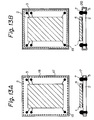
- FIGS. 2A and 2B show Prior Art 6 taught in previously mentioned Japanese Patent Laid-Open Publication No. 2-310957.
- a semiconductor device 40 is produced which has leads 37 on the opposite sides, top and bottom of a package implemented as a molding 38. Then, as shown in FIG. 2B, such semiconductor devices 40 are connected by the leads 37 in multiple stages.
- a semiconductor package stack module has LSI chips 1 implemented as 4M-DRAM chips by way of example. Each chip is sized 4.5 mm x 12.0 mm and provided with twenty-six I/O terminals.
- Ceramic carrier substrates 2 are implemented as 150 ⁇ m thick glass ceramic substrates in the illustrative embodiment. Each carrier substrate 2 is sized 5.0 mm x 13.4 mm and has wiring conductors 3 on its surface where the chip 1 is mounted, and in its inside. For the conductors 3, use is made of an Ag-Pd conductive paste.
- the carrier substrates 2 are formed with through holes 5 in their portions where the substrates 2 are electrically connected to each other. The front and rear of each carrier substrate 2 is connected together by a conductor.
- Each chip 1 and associated carrier substrate 2 are connected by bumps 4 which are implemented by a Pb-Sn solder.
- the reference numeral 12 designates a mother board.
- the above stack module was connected by the following procedure. First, the bumps 4 were formed on each chip 1. Then, a solder paste was printed on the pads of the carrier substrate 2, and then the chip 1 was set on the substrate 2. The substrate 2 and chip 1 were connected together by reflow at 230°C (FIG. 4A). The substrate 2 has a capacitor 10 thereinside. An epoxy resin or seal resin 6 was injected into the above subassembly and then hardened in order to enhance the reliability of the connecting portion and chip 1 (FIG. 4B). The chip 1 was produced from a 0.6 mm thick silicon wafer and ground, polished, surface ground, etched or otherwise treated to a thickness of 0.1 mm (FIG. 4C).
- the bumps 7 are Cu balls having a diameter of 150 ⁇ m and coated with a Pb-Sn solder. Specifically, the solder paste was printed on the pads of each substrate 2, and then the Cu balls coated with solder were arranged on the substrate 2 and fused by heat to turn out the bumps 7 (FIG. 4D). The solder paste was also printed on the other side of each substrate 2. Subsequently, four substrates 2 were stacked and heated to be thereby connected to each other and then fixed by a resin 8. The resulting stack module is shown in FIG. 4E.
- the four 4M-DRAMs stacked together implement a 16M-DRAM. Because the thickness of the module is open to choice, the individual semiconductor device can be as thin as 0.1 mm to 0.3 mm.
- the substrates 2 have desirably flat because the warp thereof is 20 ⁇ m or less.
- an Ag-Pd conductor is plated with Ni and Au in order to enhance the wettability of the solder.
- the substrates 2 are formed of glass ceramics based on lead borosilicate.
- use may be made of lead borosilicate-based steatite, forsterite, cordierite, mullite or similar insulative glass ceramics, or alumina, mullite, aluminum nitride, silicone nitride or similar ceramics.
- the substrates 2 are formed of such strong ceramics, they are substantially free from deformation during assembly. Hence, the stack module is desirable in operability and reliability.
- solder whose major component was Pb-Sn could be replaced with a solder whose major component was Sn-Ag, Sn-Zn, Au or In. Because each material has a particular melting temperature, it is necessary to select an adequate combination of solders, adequate processing temperatures, etc.
- bumps may also be implemented by the material used for the solder, use may be made of Cu-core balls or Ni-, Fe- or similar metal-core balls.
- the bumps may even be replaced with conductive pins 13, as shown in FIGS. 3B and 3C.
- the conductive adhesive may be an epoxy resin containing the particles of Ag, Cu, Au or similar conductive metal.
- each substrate 2 may be elongated in the right-and-left direction, as viewed in FIG. 3A. This allows the substrates 2 to play the role of cooling fins.
- This embodiment is similar to the first embodiment except that carrier films are substituted for the carrier substrates 2.
- the carrier films were implemented by 100 ⁇ m thick polyimide films sized 5.0 mm x 13.4 mm.
- the Cu wiring conductors 3 were formed on the surface of each carrier film where the chip 1 was mounted.
- FIG. 5A shows a single carrier substrate although a plurality of such substrates may be stacked to form a stack module.
- the substrate was made of alumina and 100 ⁇ m thick, while the wiring conductors were implemented by Mo.
- the substrate is formed with a cavity 21 for receiving an LSI chip.
- the bumps for connecting the chip to the substrate was implemented by an Au-Sn solder.
- the substrates stacked together were connected to each other by an Sn-Zn solder.
- this embodiment is similar to the third embodiment except that a carrier film is substituted for the carrier substrate.
- the wiring conductors were implemented by Cu.
- the film was 100 ⁇ m thick in its portion corresponding to the cavity 21, and 250 ⁇ m thick in the other portion.
- the carrier with the cavity 21 of the third or fourth embodiment is easy to handle in the event of stacking and protects the chip from damage. This kind of package is highly reliable.
- the nearby carriers or all the carriers in the stack may be collectively sealed by a nonconductive resin 14, except for the bumps 7 to be connected to the mother board 12. This increases the resistance of the module to moisture.
- the nonconductive resin 14 is also applicable to the carriers lacking the cavity.
- FIGS. 7A-7D show a procedure for assembling the stack of FIG. 6.
- the LSI chip 1 with metal or bumps 4 is connected face down to the carrier 2 having the cavity 21, and the electrodes of the chip 1 and those of the carrier 2 are electrically connected (FIG. 7A).
- the subassembly is sealed by the resin 6 (FIG. 7B).
- the chip 1 has its rear polished, ground, etched or otherwise treated to have a thickness of about 0.1 mm to about 0.3 mm (FIG. 7C).
- the carriers are stacked together and connected by metal, conductive resin or the like via the end through holds 5' (FIG. 7D).
- the entire stack is about 0.4 mm to 1.2 mm thick. While such a thickness is equivalent to 0.1 mm particular to a TSOP which is the thinnest package available today, this embodiment is about four times as high as the TSOP in packaging density and feasible for a high density semiconductor device.
- FIG. 8 shows a single carrier substrate 2 although a plurality of such substrates may be stacked to form a stack module.
- the LSI chip 1 is bonded to the semiconductor pads of the substrate 2 face down via the bumps 4.
- the ceramic substrate 2 was 200 ⁇ m thick. Increases in processing speed and packaging density make it necessary to release heat generated by the chip 1 and to match the characteristic impedance.
- a conductor layer 11 is formed on the side of the substrate 2 opposite to the side for mounting the chip 1.
- the conductor layer 11 may be implemented as a conductive heat radiator, in which case the layer 11 may be connected to ground. While the conductive layer 11 is W in the embodiment, the above object is achievable even if use is made of metal whose major component is Ag, Au, Cu, Ag-Pd, Mo or the like.
- the ceramic carrier 2 is formed of aluminum nitride.
- the carrier 2 may be formed of any other glass ceramics or ceramics mentioned in relation to the first embodiment.
- the wiring conductors 3 were based on W.
- the bumps 4 and 7 were implemented by Ag-core balls coated with an Sn-Ag solder and Au, respectively.
- this embodiment is similar to the sixth embodiment except that the ceramic carrier substrate 2 is replaced with a 50 ⁇ m thick polyimide carrier film 2.
- a heat radiator 9 is formed on the side of the film 2 opposite to the side for mounting the chip 1.
- the heat radiator 9, it is possible to radiate the heat and to match the characteristic impedance for reducing electric noise.
- the heat radiator, or conductive layer, 9 may be formed in a solid, mesh or similar pattern. While the heat radiator 9 is a copper sheet in the embodiment, use may be made of a sheet of nickel, stainless steel, tungsten, aluminum, molybdenum or similar metal. Further, as shown in FIGS. 9B and 9C, the heat radiator 9 may be bonded by metal or resin having high thermal conductivity to the rear of the individual chip I thinned to a desired thickness.
- the bumps 7 and 4 were implemented by Ag-core balls coated with an Sn-Ag solder and Au, respectively.
- a Cu conductor was plated with Ni and Au.
- FIGS. 10a and 10B show an embodiment in which the carriers 2 arranged in a stack each has a heat radiating effect.
- each heat radiator 9 is elongated in order to enhance the heat radiating effect. Because the heat radiating effect of the heat radiator 9 increases with an increase in the thickness of the radiator 9, the distance between the chip 1 and the carrier 2 should preferably be zero. If the distance is not zero, a compound, silicone rubber or oil having high thermal conductivity may be filled in the gap between the chip 1 and the carrier 2.
- FIGS. 10A and 10B show each heat radiator 9 as contacting the rear of the associated chip 1, the heat radiator 9 may, of course, contact the rear of the carrier 2.
- the chips 1 each having the respective heat radiator 9 are mounted on the mother board 12.
- the surface of the heat radiator 9 and the rear of the associated carrier 2 may be bonded by metal or resin having high thermal conductivity, as shown in FIG. 11A, or may be connected together by bumps, as shown in FIG. 11B.
- This kind of structure implements a semiconductor package stack module having a high density and releasing heat efficiently.
- electrodes 15 formed on the uppermost carrier substrate 2 are covered with an insulator 16, e.g., a polyimide type sheet.
- the insulator 16 is provided with an adhesive layer on its one side. In this condition, even when a conductive impurity deposits on any of the electrodes 15, the package is free from short-circuiting. After the stack has been mounted to the mother board, the insulator 16 may be removed in order to use the electrodes 15 as test pads.
- FIG. 13A shows the carrier 2 formed with though holes 17 at a fine pitch, in addition to the through holes 5 adapted for carrier connection.
- the through holes 17 are interconnected by a conductor 18, and all of them are connected to a ground terminal 19.
- FIG. 13B shows the carrier 2 provided with a conductive layer 20 along its edges.
- the conductive layer 20 is connected to the ground terminal 19.
- the conductive layer 20 surrounds the chip 1 and thereby prevents it from interfering with another chip 1.
- a multicarrier body is formed with a number of carriers 2 shown in FIGS. 4A-4E or 7A-7D.
- the chips 1 are connected to the multicarrier body by bumps.
- the seal resin 6 is injected between each chip 1 and the associated carrier 2.
- the rear of each chip 1 is ground, polished, etched or otherwise treated to provide the chip 1 with a desired thickness.
- the bumps 7 having a desired height are formed by a solder ball method, solder paste printing method, dispensing method, or similar technology.
- Terminals extending out from the individual chip 1 to the associated carrier 2 are used to test the electric characteristic before, during, or after a burn-in test. It is to be noted that such a test can be effected at any desired stage after the chips 1 have been mounted on the multicarrier body. A desired number of carriers undergone the above test are positioned. The carriers are connected together by reflow, welding or similar technology when the connection is implemented by metal, or they are connected by thermosetting, ultraviolet rays setting or similar technology when use is made of a conductive resin.
- the individual semiconductor device is produced by dicing, laser, scribing, choco-braking, or similar technology.
- the initial multicarrier body is formed with brake grooves.
- an electric characteristic test is performed, as needed. For the test, electrical contact with pads for stack connection and formed on the top, bottom and opposite sides of the individual carrier is set up by a probe or surface-to-surface contact.
- the present invention provides a semiconductor package stack module and a method of producing it which have various unprecedented advantages, as enumerated below.
Abstract
In a semiconductor package stack module, an LSI (Large Scale Integrated circuit) is mounted, via fine bumps, on a ceramic carrier substrate or a flexible carrier film on which wiring conductors are formed. After a seal resin has been injected, the chip is thinned by, e.g., grinding. A plurality of such carrier substrates or carrier films are connected to each other by bumps via through holes which are electrically connected to the wiring conductors, thereby completing a tridimensional stack module. The module achieves a miniature, thin, dense, low cost, and reliable structure without resorting to a wire bonding system or a TAB (Tape Automated Bonding) system. In addition, the module has a minimum of wiring length and a desirable electric characteristic.


Description
- The present invention relates to a semiconductor package with an LSI (Large Scale Integrated circuit) mounted thereon, and a method of producing the same. More particularly, the present invention is concerned with a semiconductor package stack module having LSI chips stacked tridimensionally in a high density, and a method of producing the same.
- Various stack module structures for semiconductor packages and methods for producing them are known in the art, as follows.
- (1) TSOPs (Thin Small Out line Packages) or similar mold packages are stacked and connected together by leads extending out from the packages (Prior Art 1).
- (2) LSI chips are directly stacked together (Prior Art 2). This kind of scheme uses wire bonding, and therefore provides the ends of the chips with a configuration suitable for bonding. The chips are mounted on a carrier substrate and connected to the substrate by wires.
- (3) Chips connected by TAB (Tape Automated Bonding) are stacked in a module configuration (Prior Art 3). In this case, TAB leads are bent and connected to a carrier substrate.
- (4) Semiconductor elements connected by TAB are connected to the islands of a lead frame in a stack, and the entire assembly is sealed by a resin (Prior Art 4).
- (5) Japanese Patent Laid-Open Publication No. 61-101067 discloses a memory module structure (Prior Art 5). Specifically, memory ICs are mounted on ceramic packages each having a cavity and formed with electrodes for IC connection and electrodes for chip carrier connection. The electrodes for chip carrier connection are electrically connected to the IC and IC electrodes by thin metallic wires, and the resulting subassembly is sealed by a resin. A plurality of carriers each having an electrode pattern on its outer periphery for leading the electrodes to the outside are stacked. Subsequently, the electrode patterns are electrically connected to each other. The chips are connected by wire bonding while the carriers are connected via the outer walls of a carrier container.
- (6) Japanese Patent Laid-Open Publication No. 2-310957 teaches a semiconductor device having a conventional mold package which is provided with leads on its opposite sides, top and bottom (Prior Art 6). A plurality of such semiconductor devices are stacked and connected by leads.
- (7) Metal for stack connection is formed on the end faces of semiconductor elements by lithography, oxidation, metal forming or similar technology.
- (8) A QFP carrying memory semiconductor elements in a multitip configuration is produced. Such QFPs are stacked and connected by the leads of the QFPs.
- (9) Conventional IC packages are stacked and connected by subboards and a mother board.
- The prior art technologies described above have the following problems.
- (1)
Prior Art 1 has a problem that each package has a substantial thickness, resulting in an extremely thick module. Because the chips are connected by wire bonding, the molded configuration is too great to promote miniaturization. - (2)
Prior Art 2 must bond the chips one by one, and therefore increases the time and cost for production. Moreover, because bare chips are stacked, the individual chip cannot be tested until the entire module has been assembled. In addition, the ends of the chips must be machined for wire bonding. - (3) Although Prior Art 3 allows a test to be effected with the individual TAB chip, mounting the chips one by one increases the cost. Further, the resulting module is bulky. Because the TAB chips are higher in level than ordinary QFP packages when stacked together, a high packing density is not achievable. In addition, TAB makes various kinds of handling, including mounting, difficult.
- (4)
Prior Art 4 is expensive, and moreover requires strong semiconductor elements due to the TAB connection. Hence, the semiconductor elements must be provided with a certain thickness and cannot be thinned to below about 0.3 mm. As a result, the entire QFP package cannot be reduced in thickness. - (5)
Prior Art 5 also relies on wire bonding. This, coupled with the fact that the carrier containers are connected via their outer walls, increases the size of the module and the wiring length. Further, because each chip carrier has a height more than several times as great as as the thickness of the individual semiconductor device before stacking, the module is not feasible for dense packaging. In addition, connecting the semiconductor devices in multiple stages further lowers the packaging density. - (6)
Prior Art 6 disposes a semiconductor element in a mold resin in an inclined position. Hence, the thickness of the mold is several times as greater as the total thickness of the semiconductor element and lead frame. This also obstructs dense packaging. Connecting such semiconductor elements in multiple stages further lowers the packaging density. - (7)
Prior Art 7 is technically difficult to practice and needs prohibitive facility investments. - (8) Prior Art 8 is not suitable for dense packaging because the individual QFP package is several times as thick as the semiconductor element. Connecting the packages in multiple stages further lowers the packaging density.
- (9)
Prior Art 9 simply connects IC packages having the conventional thickness in multiple stages, and therefore fails to enhance dense packaging. In addition, the subboards and mother board further lower the packaging density. - It is therefore an object of the present invention to provide a miniature, thin, dense, low cost, and reliable semiconductor package stack module needing a minimum of wiring length and achieving a desirable electric characteristic, and a method of producing the same.
- In accordance with the present invention, a semiconductor package has a carrier, through holes formed in the carrier or at the end faces of the carrier, a conductor pattern formed at least on the front of the carrier, pads for inner bonding, and formed on the rear of the carrier, and electrically connected to the through holes, and an LSI chip connected to the carrier by the pads.
- Also, in accordance with the present inveniton, in a semiconductor package stack module having a plurality of carriers stacked one upon the other, the carriers each has through holes formed in or at the end faces of the carrier, a conductor pattern formed at least on the front of the carrier, pads for inner bonding, and formed on the rear of the carrier, and electrically connected to the through holes, and an LSI chip connected to the carrier by the pads. The carriers are connected tridimensionally by the through holes.
- Further, in accordance with the present invention, a method of producing a semiconductor package stack module has the steps of connecting a ceramic carrier substrate and an LSI chip, injecting a seal resin between the ceramic carrier substrate and the LSI chip which are formed with bumps each, reducing the thickness of the LSI chip mounted on the ceramic carrier substrate by one of polishing, grinding, surface grinding, and etching, and stacking and soldering a plurality of ceramic carrier substrates each carrying the respective LSI chip.
- Moreover, in accordance with the present invention, in a semiconductor package stack module, a multicarrier body formed with a plurality of carriers not separated from each other is subjected to mounting of LSI chips, connection of the LSI chips and carriers via bumps, sealing with resin, thinning, burn-in tests, multistage connection, and electric characteristic tests, and then the plurality of carriers are separated from each other by one of laser, scribing, dicing, and choco-braking.
- The above and other objects, features and advantages of the present invention will become more apparent from the following detailed description taken with the accompanying drawings in which:
- FIGS. 1 and 2 each shows a particular conventional semiconductor package stack module;
- FIGS. 3A-3C show a first and a second embodiment of the semiconductor package stack module in accordance with the present invention;
- FIGS. 4A-4E show a sequence of steps for producing the module shown in FIGS. 3A-3E;
- FIGS. 5A-5D show a third and a fourth embodiment of the present invention;
- FIG. 6 shows a fifth embodiment of the present invention;
- FIGS. 7A-7D demonstrate a sequence of steps for producing the module of the fifth embodiment;
- FIG. 8 shows a sixth embodiment of the present invention;
- FIGS. 9A-9C show a seventh embodiment of the present invention;
- FIGS. 10A and 10B show an eighth embodiment of the present invention;
- FIGS. 11A and 11B show a ninth embodiment of the present invention;
- FIG. 12 shows a tenth embodiment of the present invention; and
- FIGS. 13A and 13B show an eleventh embodiment of the present invention.
- To better understand the present invention, a brief reference will be made to a conventional semiconductor package stack module, shown in FIG. 1. As shown, the module has
memory ICs 34 mounted on respective ceramic packages. The ceramic packages each has a cavity and is formed withelectrodes 32 for IC connection andelectrodes 33 for chip carrier connection. Theelectrodes 33 are electrically connected to theIC 34 andIC electrodes 32 by thin metallic wires, and the resulting subassembly is sealed by aresin 35. A plurality of carriers each having an electrode pattern on its outer periphery for leading the electrodes to the outside are stacked. Subsequently, the electrode patterns are electrically connected to each other. The reference numerals 31 and 36 designate ceramics and a solder, respectively. Thechips 34 are connected by wire bonding while the carriers are connected via the outer walls of a carrier container. - FIGS. 2A and 2B show
Prior Art 6 taught in previously mentioned Japanese Patent Laid-Open Publication No. 2-310957. As shown in FIG. 2A, asemiconductor device 40 is produced which has leads 37 on the opposite sides, top and bottom of a package implemented as amolding 38. Then, as shown in FIG. 2B,such semiconductor devices 40 are connected by theleads 37 in multiple stages. - However, the above conventional structures have various problems, as discussed earlier.
- Preferred embodiments of the semiconductor package stack module in accordance with the present invention will be described hereinafter. In the embodiments, the s a m e structural parts are designated by like reference numerals.
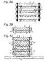
- As shown in FIGS. 3A-3C, a semiconductor package stack module has
LSI chips 1 implemented as 4M-DRAM chips by way of example. Each chip is sized 4.5 mm x 12.0 mm and provided with twenty-six I/O terminals.Ceramic carrier substrates 2 are implemented as 150 µm thick glass ceramic substrates in the illustrative embodiment. Eachcarrier substrate 2 is sized 5.0 mm x 13.4 mm and haswiring conductors 3 on its surface where thechip 1 is mounted, and in its inside. For theconductors 3, use is made of an Ag-Pd conductive paste. Thecarrier substrates 2 are formed with throughholes 5 in their portions where thesubstrates 2 are electrically connected to each other. The front and rear of eachcarrier substrate 2 is connected together by a conductor. Eachchip 1 and associatedcarrier substrate 2 are connected bybumps 4 which are implemented by a Pb-Sn solder. Thereference numeral 12 designates a mother board. - The above stack module was connected by the following procedure. First, the
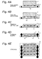
bumps 4 were formed on eachchip 1. Then, a solder paste was printed on the pads of thecarrier substrate 2, and then thechip 1 was set on thesubstrate 2. Thesubstrate 2 andchip 1 were connected together by reflow at 230°C (FIG. 4A). Thesubstrate 2 has acapacitor 10 thereinside. An epoxy resin or sealresin 6 was injected into the above subassembly and then hardened in order to enhance the reliability of the connecting portion and chip 1 (FIG. 4B). Thechip 1 was produced from a 0.6 mm thick silicon wafer and ground, polished, surface ground, etched or otherwise treated to a thickness of 0.1 mm (FIG. 4C). - Four
carrier substrates 2 each carrying the thinnedchip 1 thereon were stacked and electrically connected bybumps 7. Thebumps 7 are Cu balls having a diameter of 150 µm and coated with a Pb-Sn solder. Specifically, the solder paste was printed on the pads of eachsubstrate 2, and then the Cu balls coated with solder were arranged on thesubstrate 2 and fused by heat to turn out the bumps 7 (FIG. 4D). The solder paste was also printed on the other side of eachsubstrate 2. Subsequently, foursubstrates 2 were stacked and heated to be thereby connected to each other and then fixed by a resin 8. The resulting stack module is shown in FIG. 4E. - In the illustrative embodiment, the four 4M-DRAMs stacked together implement a 16M-DRAM. Because the thickness of the module is open to choice, the individual semiconductor device can be as thin as 0.1 mm to 0.3 mm.
- In the embodiment, the
substrates 2 have desirably flat because the warp thereof is 20 µm or less. In the connecting portions of thesubstrates 2, an Ag-Pd conductor is plated with Ni and Au in order to enhance the wettability of the solder. - In the embodiment, the
substrates 2 are formed of glass ceramics based on lead borosilicate. Alternatively, use may be made of lead borosilicate-based steatite, forsterite, cordierite, mullite or similar insulative glass ceramics, or alumina, mullite, aluminum nitride, silicone nitride or similar ceramics. When thesubstrates 2 are formed of such strong ceramics, they are substantially free from deformation during assembly. Hence, the stack module is desirable in operability and reliability. - The solder whose major component was Pb-Sn could be replaced with a solder whose major component was Sn-Ag, Sn-Zn, Au or In. Because each material has a particular melting temperature, it is necessary to select an adequate combination of solders, adequate processing temperatures, etc.
- While the bumps may also be implemented by the material used for the solder, use may be made of Cu-core balls or Ni-, Fe- or similar metal-core balls. The bumps may even be replaced with
conductive pins 13, as shown in FIGS. 3B and 3C. - Further, the
chip 1 andsubstrate 2 and thesubstrates 2 themselves may be connected by a conductive adhesive. The conductive adhesive may be an epoxy resin containing the particles of Ag, Cu, Au or similar conductive metal. - In FIG. 3A, when alumina, glass ceramics, aluminum nitride or similar material having high thermal conductivity is used, each
substrate 2 may be elongated in the right-and-left direction, as viewed in FIG. 3A. This allows thesubstrates 2 to play the role of cooling fins. - This embodiment is similar to the first embodiment except that carrier films are substituted for the
carrier substrates 2. The carrier films were implemented by 100 µm thick polyimide films sized 5.0 mm x 13.4 mm. TheCu wiring conductors 3 were formed on the surface of each carrier film where thechip 1 was mounted. - Four carrier films each having the above configuration and carrying the thinned
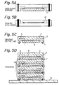
chip 1 thereon were electrically connected together by thebumps 7, as follows. For thebumps 7, use was made of Cu balls having a diameter of 150 µm and coated with a Pb-Sn solder. After the paste had been printed on the pads of the front and rear of each film, the Cu balls coated with the solder were arranged on the film. Subsequently, the films were stacked and heated to have the solder thereof melted. As a result, the film were connected together in the form of a module. In the connecting portions of the films, a Cu conductor was plated with Ni and Au in order to enhance the wettability of the solder. - FIG. 5A shows a single carrier substrate although a plurality of such substrates may be stacked to form a stack module. In this embodiment, the substrate was made of alumina and 100 µm thick, while the wiring conductors were implemented by Mo. As shown, the substrate is formed with a
cavity 21 for receiving an LSI chip. The bumps for connecting the chip to the substrate was implemented by an Au-Sn solder. The substrates stacked together were connected to each other by an Sn-Zn solder. - As shown in FIG. 5B, this embodiment is similar to the third embodiment except that a carrier film is substituted for the carrier substrate. The wiring conductors were implemented by Cu. The film was 100 µm thick in its portion corresponding to the
cavity 21, and 250 µm thick in the other portion. - The carrier with the
cavity 21 of the third or fourth embodiment is easy to handle in the event of stacking and protects the chip from damage. This kind of package is highly reliable. - As shown in FIGS. 5C and 5D, the nearby carriers or all the carriers in the stack may be collectively sealed by a nonconductive resin 14, except for the
bumps 7 to be connected to themother board 12. This increases the resistance of the module to moisture. Of course, the nonconductive resin 14 is also applicable to the carriers lacking the cavity. - As shown in FIG. 6, this embodiment is similar to the first and second embodiments except that each carrier has a cavity and end through holes 5'. FIGS. 7A-7D show a procedure for assembling the stack of FIG. 6. The
LSI chip 1 with metal orbumps 4 is connected face down to thecarrier 2 having thecavity 21, and the electrodes of thechip 1 and those of thecarrier 2 are electrically connected (FIG. 7A). Then, the subassembly is sealed by the resin 6 (FIG. 7B). Subsequently, thechip 1 has its rear polished, ground, etched or otherwise treated to have a thickness of about 0.1 mm to about 0.3 mm (FIG. 7C). Finally, the carriers are stacked together and connected by metal, conductive resin or the like via the end through holds 5' (FIG. 7D). - In the above procedure, when four carriers are stacked, the entire stack is about 0.4 mm to 1.2 mm thick. While such a thickness is equivalent to 0.1 mm particular to a TSOP which is the thinnest package available today, this embodiment is about four times as high as the TSOP in packaging density and feasible for a high density semiconductor device.
- FIG. 8 shows a
single carrier substrate 2 although a plurality of such substrates may be stacked to form a stack module. As shown, theLSI chip 1 is bonded to the semiconductor pads of thesubstrate 2 face down via thebumps 4. Theceramic substrate 2 was 200 µm thick. Increases in processing speed and packaging density make it necessary to release heat generated by thechip 1 and to match the characteristic impedance. In light of this, in this embodiment, aconductor layer 11 is formed on the side of thesubstrate 2 opposite to the side for mounting thechip 1. Theconductor layer 11 may be implemented as a conductive heat radiator, in which case thelayer 11 may be connected to ground. While theconductive layer 11 is W in the embodiment, the above object is achievable even if use is made of metal whose major component is Ag, Au, Cu, Ag-Pd, Mo or the like. - In this embodiment, the
ceramic carrier 2 is formed of aluminum nitride. However, thecarrier 2 may be formed of any other glass ceramics or ceramics mentioned in relation to the first embodiment. Thewiring conductors 3 were based on W. Thebumps - As shown in FIGS. 9A-9C, this embodiment is similar to the sixth embodiment except that the
ceramic carrier substrate 2 is replaced with a 50 µm thickpolyimide carrier film 2. To release the heat, aheat radiator 9 is formed on the side of thefilm 2 opposite to the side for mounting thechip 1. With theheat radiator 9, it is possible to radiate the heat and to match the characteristic impedance for reducing electric noise. The heat radiator, or conductive layer, 9 may be formed in a solid, mesh or similar pattern. While theheat radiator 9 is a copper sheet in the embodiment, use may be made of a sheet of nickel, stainless steel, tungsten, aluminum, molybdenum or similar metal. Further, as shown in FIGS. 9B and 9C, theheat radiator 9 may be bonded by metal or resin having high thermal conductivity to the rear of the individual chip I thinned to a desired thickness. - While the
wiring conductors 3 were also made of Cu, thebumps bumps 7, a Cu conductor was plated with Ni and Au. - FIGS. 10a and 10B show an embodiment in which the
carriers 2 arranged in a stack each has a heat radiating effect. As shown in FIG. 10B, eachheat radiator 9 is elongated in order to enhance the heat radiating effect. Because the heat radiating effect of theheat radiator 9 increases with an increase in the thickness of theradiator 9, the distance between thechip 1 and thecarrier 2 should preferably be zero. If the distance is not zero, a compound, silicone rubber or oil having high thermal conductivity may be filled in the gap between thechip 1 and thecarrier 2. - While FIGS. 10A and 10B show each
heat radiator 9 as contacting the rear of the associatedchip 1, theheat radiator 9 may, of course, contact the rear of thecarrier 2. - As shown in FIGS. 11A and 11B, the
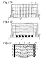
chips 1 each having therespective heat radiator 9 are mounted on themother board 12. The surface of theheat radiator 9 and the rear of the associatedcarrier 2 may be bonded by metal or resin having high thermal conductivity, as shown in FIG. 11A, or may be connected together by bumps, as shown in FIG. 11B. This kind of structure implements a semiconductor package stack module having a high density and releasing heat efficiently. - As shown in FIG. 12,
electrodes 15 formed on theuppermost carrier substrate 2 are covered with aninsulator 16, e.g., a polyimide type sheet. Theinsulator 16 is provided with an adhesive layer on its one side. In this condition, even when a conductive impurity deposits on any of theelectrodes 15, the package is free from short-circuiting. After the stack has been mounted to the mother board, theinsulator 16 may be removed in order to use theelectrodes 15 as test pads. - FIG. 13A shows the
carrier 2 formed with thoughholes 17 at a fine pitch, in addition to the throughholes 5 adapted for carrier connection. The through holes 17 are interconnected by aconductor 18, and all of them are connected to aground terminal 19. On the other hand, FIG. 13B shows thecarrier 2 provided with a conductive layer 20 along its edges. The conductive layer 20 is connected to theground terminal 19. The conductive layer 20 surrounds thechip 1 and thereby prevents it from interfering with anotherchip 1. - A multicarrier body is formed with a number of
carriers 2 shown in FIGS. 4A-4E or 7A-7D. Thechips 1 are connected to the multicarrier body by bumps. Then, theseal resin 6 is injected between eachchip 1 and the associatedcarrier 2. Subsequently, in the multicarrier configuration, the rear of eachchip 1 is ground, polished, etched or otherwise treated to provide thechip 1 with a desired thickness. - In the above multicarrier body, the
bumps 7 having a desired height are formed by a solder ball method, solder paste printing method, dispensing method, or similar technology. - Terminals extending out from the
individual chip 1 to the associatedcarrier 2 are used to test the electric characteristic before, during, or after a burn-in test. It is to be noted that such a test can be effected at any desired stage after thechips 1 have been mounted on the multicarrier body. A desired number of carriers undergone the above test are positioned. The carriers are connected together by reflow, welding or similar technology when the connection is implemented by metal, or they are connected by thermosetting, ultraviolet rays setting or similar technology when use is made of a conductive resin. - Subsequently, the individual semiconductor device is produced by dicing, laser, scribing, choco-braking, or similar technology. Regarding the choco-braking method, the initial multicarrier body is formed with brake grooves. Finally, an electric characteristic test is performed, as needed. For the test, electrical contact with pads for stack connection and formed on the top, bottom and opposite sides of the individual carrier is set up by a probe or surface-to-surface contact.
- While the foregoing embodiments have concentrated on D-RAM chips, the present invention is practicable even with microcomputers, gate arrays and other LSI chips.
- In summary, it will be seen that the present invention provides a semiconductor package stack module and a method of producing it which have various unprecedented advantages, as enumerated below.
- (1) The module is small size, thin, and dense and has a desirable electric characteristic. Carriers have a minimum of wiring length either individually or in a stack.
- (2) A desired number of carrier substrates or carrier films each carrying a respective chip are collectively stacked and connected to form the module. This promotes efficient operations and reduces production cost. The carriers may each have its circuit pattern partly connected or partly separated so as to have a particular circuit function. Then, if a particular symbol or number is provided on each carrier, the electric circuits can be combined in a desired manner.
- (3) Because an LSI chip is mounted on the individual carrier substrate or carrier film, the chip can be tested on the carrier basis. Hence, only the acceptable products can be stacked. A desired number of carrier substrates or carrier films each carrying a respective chip are collectively stacked and connected to form the module. This promotes efficient operations and reduces production cost. In addition, bumps for chip connection can be implemented by a solder having a high melting point.
- (4) The package releases heat in a desirable manner and has a matched characteristic impedance.
- (5) When ceramic carriers are used, the substrates are desirably flat and resistive to moisture. Further, the ceramic carriers are easy to handle during assembly. Moreover, this kind of carriers promote reliable connection because their surfaces remain flat during the course of reflow.
- Various modifications will become possible for those skilled in the art after receiving the teachings of the present disclosure without departing from the scope thereof.
Claims (31)
- A semiconductor package comprising:a carrier;through holes formed in said carrier or at end faces of said carrier;a conductor pattern formed at least on a front of said carrier;pads for inner bonding, and formed on a rear of said carrier, and electrically connected to said through holes; andan LSI chip connected to said carrier by said pads.
- A semiconductor package as claimed in claim 1, wherein said through holes are formed in said carrier and connected tridimensionally by electrically connected pumps for carrier connection.
- A semiconductor package as claimed in claim 1, wherein said LSI chip is mounted on said carrier face down, and wherein said pads for inner bonding comprise bumps.
- A semiconductor package as claimed in claim 3, wherein said pads for inner bonding and said bumps for carrier connection are formed of a solder whose major component is Pb-Sn, Sn-Ag, Sn-Zn, Au-Sn, Au, or In.
- A semiconductor package as claimed in claim 1, further comprising a heat radiator closely contacting one of said carrier and said LSI chip.
- A semiconductor package as claimed in claim 5, further comprising a conductor pattern closely contacting said carrier.
- A semiconductor package as claimed in claim 6, wherein said conductor pattern is connected to ground.
- A semiconductor package as claimed in claim 1, wherein said carrier includes a cavity for receiving said LSI chip.
- A semiconductor package as claimed in claim 8, wherein said cavity has a depth greater than a height of bumps formed on said LSI chip.
- A semiconductor package as claimed in claim 1, wherein said carrier accommodates a capacitor thereinside.
- A semiconductor package as claimed in claim 10, wherein said capacitor is electrically connected between a power source and ground.
- A semiconductor package as claimed in claim 1, wherein said carrier comprises one of a film-like substrate of sintered ceramics, a flexible film, and a printed circuit board.
- A semiconductor package as claimed in claim 12, further comprising an insulator covering terminal electrodes formed on a front of an uppermost layer of said semiconductor package.
- A semiconductor package as claimed in claim 1, further comprising a conductor layer formed on and along edge portions of said carrier and connected to ground.
- A semiconductor package as claimed in claim 1, further comprising through holes formed in arrays in edge portions of said carrier at a fine pitch and connected to ground without exception.
- In a semiconductor package stack module having a plurality of carriers stacked one upon the other, said plurality of carriers each comprises through holes formed in or at end faces of said carrier, a conductor pattern formed at least on a front of said carrier, pads for inner bonding, and formed on a rear of said carrier, and electrically connected to said through holes, and an LSI chip connected to said carrier by said pads, said plurality of carriers being connected tridimensionally by said through holes.
- A module as claimed in claim 16, wherein said through holes are formed in said carrier and connected tridimensionally by electrically connected pumps for carrier connection.
- A module as claimed in claim 16, wherein said LSI chip is mounted on said carrier face down, and wherein said pads for inner bonding comprise bumps.
- A module as claimed in claim 18, wherein said pads for inner bonding and said bumps for carrier connection are formed of a solder whose major component is Pb-Sn, Sn-Ag, Sn-Zn, Au-Sn, Au, or In.
- A module as claimed in claim 16, further comprising a heat radiator interposed between said LSI chip mounted on any one of said plurality of carriers and another carrier adjoining said one carrier, and closely contacting said carrier or said LSI chip.
- A module as claimed in claim 20, further comprising a conductor pattern closely contacting said carrier.
- A module as claimed in claim 21, further comprising a material having high thermal conductivity and interposed between one of said LSI chip and said carrier and said heat radiator.
- A module as claimed in claim 16, wherein a seal resin is filled between each LSI chip subjected to inner connection and associated one of said carriers.
- A module as claimed in claim 16, wherein said carriers each accommodates a capacitor therein.
- A module as claimed in claim 24, wherein said capacitor is electrically connected to a power source and ground.
- A module as claimed in claim 16, wherein said carrier comprises one of a film-like substrate of sintered ceramics, a flexible film, and a printed circuit board.
- A module as claimed in claim 16, further comprising an insulator covering terminal electrodes formed on a front of an uppermost carrier.
- A module as claimed in claim 16, further comprising a conductor layer formed on and along edge portions of said carrier and connected to ground.
- A module as claimed in claim 16, further comprising through holes formed in arrays in edge portions of said carrier at a fine pitch and connected to ground without exception.
- A method of producing a semiconductor package stack module, comprising the steps of:(a) connecting a ceramic carrier substrate and an LSI chip;(b) injecting a seal resin between said ceramic carrier substrate and said LSI chip which are formed with bumps each;(c) reducing a thickness of said LSI chip mounted on said ceramic carrier substrate by one of polishing, grinding, surface grinding, and etching; and(d) stacking and soldering a plurality of ceramic carrier substrates each carrying a respective LSI chip.
- In a semiconductor package stack module, a multicarrier body formed with a plurality of carriers not separated from each other is subjected to mounting of LSI chips, connection of said LSI chips and said plurality of carriers via bumps, sealing with resin, thinning, burn-in tests, multistage connection, and electric characteristic tests, and then said plurality of carriers are separated from each other by one of laser, scribing, dicing, and choco-braking.
Applications Claiming Priority (3)
| Application Number | Priority Date | Filing Date | Title |
|---|---|---|---|
| JP3666495 | 1995-02-24 | ||
| JP36664/95 | 1995-02-24 | ||
| JP7036664A JP2944449B2 (en) | 1995-02-24 | 1995-02-24 | Semiconductor package and manufacturing method thereof |
Publications (2)
| Publication Number | Publication Date |
|---|---|
| EP0729184A2 true EP0729184A2 (en) | 1996-08-28 |
| EP0729184A3 EP0729184A3 (en) | 1999-11-03 |
Family
ID=12476134
Family Applications (1)
| Application Number | Title | Priority Date | Filing Date |
|---|---|---|---|
| EP96102773A Withdrawn EP0729184A3 (en) | 1995-02-24 | 1996-02-23 | Semiconductor package stack module and method of producing the same |
Country Status (5)
| Country | Link |
|---|---|
| US (1) | US6188127B1 (en) |
| EP (1) | EP0729184A3 (en) |
| JP (1) | JP2944449B2 (en) |
| KR (1) | KR100231366B1 (en) |
| TW (1) | TW312844B (en) |
Cited By (11)
| Publication number | Priority date | Publication date | Assignee | Title |
|---|---|---|---|---|
| EP0915516A2 (en) * | 1997-10-30 | 1999-05-12 | Nec Corporation | Substrate for stacked module and stacked module |
| WO1999057765A1 (en) * | 1998-05-05 | 1999-11-11 | Dense-Pac Microsystems, Inc. | Chip stack and method of making same |
| EP1028463A1 (en) * | 1999-01-18 | 2000-08-16 | Kabushiki Kaisha Toshiba | Flexible package having very thin semiconductor chip, module and multi chip module (MCM) assembled by the package, and method for manufacturing the same |
| EP1137066A2 (en) * | 2000-03-24 | 2001-09-26 | Shinko Electric Industries Co. Ltd. | Semiconductor device and process of production of same |
| US6506664B1 (en) | 1999-04-02 | 2003-01-14 | Imec Vzw | Method of transferring ultra-thin substrates and application of the method to the manufacture of a multi-layer thin film device |
| KR100556177B1 (en) * | 2000-09-05 | 2006-03-03 | 세이코 엡슨 가부시키가이샤 | Semiconductor device and method of manufacture thereof, circuit board, and electronic instrument |
| CN102945821A (en) * | 2012-11-28 | 2013-02-27 | 贵州振华风光半导体有限公司 | Integrating method of high-density thick-film hybrid integrated circuit |
| CN103094219A (en) * | 2012-11-28 | 2013-05-08 | 贵州振华风光半导体有限公司 | Integration method for three-dimensional high-density thick-film multi-chip assembly |
| EP2693477A1 (en) * | 2011-12-21 | 2014-02-05 | Huawei Technologies Co., Ltd | Pop encapsulation structure |
| EP3055881A4 (en) * | 2014-12-15 | 2017-09-13 | INTEL Corporation | Opossum-die package-on-package apparatus |
| CN113410193A (en) * | 2021-05-27 | 2021-09-17 | 力成科技(苏州)有限公司 | 8+1 heap chip package device |
Families Citing this family (144)
| Publication number | Priority date | Publication date | Assignee | Title |
|---|---|---|---|---|
| JP2728074B2 (en) * | 1995-12-28 | 1998-03-18 | 日本電気株式会社 | Stack structure of tape carrier package |
| DE19626126C2 (en) * | 1996-06-28 | 1998-04-16 | Fraunhofer Ges Forschung | Method for forming a spatial chip arrangement and spatial chip arrangement |
| CN1171298C (en) | 1996-11-21 | 2004-10-13 | 株式会社日立制作所 | Semiconductor device and process for manufacturing same |
| KR100381836B1 (en) * | 1996-12-13 | 2003-07-18 | 앰코 테크놀로지 코리아 주식회사 | Semiconductor package |
| JPH10294423A (en) | 1997-04-17 | 1998-11-04 | Nec Corp | Semiconductor device |
| JP2000208698A (en) | 1999-01-18 | 2000-07-28 | Toshiba Corp | Semiconductor device |
| US6274929B1 (en) * | 1998-09-01 | 2001-08-14 | Texas Instruments Incorporated | Stacked double sided integrated circuit package |
| US6451624B1 (en) * | 1998-06-05 | 2002-09-17 | Micron Technology, Inc. | Stackable semiconductor package having conductive layer and insulating layers and method of fabrication |
| US6297548B1 (en) * | 1998-06-30 | 2001-10-02 | Micron Technology, Inc. | Stackable ceramic FBGA for high thermal applications |
| KR100424188B1 (en) * | 1998-09-21 | 2004-05-17 | 주식회사 하이닉스반도체 | Chip size stack package |
| US6461895B1 (en) * | 1999-01-05 | 2002-10-08 | Intel Corporation | Process for making active interposer for high performance packaging applications |
| US6600364B1 (en) | 1999-01-05 | 2003-07-29 | Intel Corporation | Active interposer technology for high performance CMOS packaging application |
| JP2000216334A (en) | 1999-01-25 | 2000-08-04 | Seiko Epson Corp | Semiconductor device |
| JP3627565B2 (en) * | 1999-03-30 | 2005-03-09 | セイコーエプソン株式会社 | Semiconductor device and manufacturing method thereof |
| JP2000315866A (en) * | 1999-04-30 | 2000-11-14 | Ibiden Co Ltd | Multilayer wiring board and manufacture thereof |
| JP2000340737A (en) * | 1999-05-31 | 2000-12-08 | Mitsubishi Electric Corp | Semiconductor package and body mounted therewith |
| KR100333384B1 (en) | 1999-06-28 | 2002-04-18 | 박종섭 | chip size stack package and method of fabricating the same |
| KR100333385B1 (en) | 1999-06-29 | 2002-04-18 | 박종섭 | wafer level stack package and method of fabricating the same |
| WO2001008222A1 (en) | 1999-07-22 | 2001-02-01 | Seiko Epson Corporation | Semiconductor device, method of manufacture thereof, circuit board, and electronic device |
| TW417839U (en) * | 1999-07-30 | 2001-01-01 | Shen Ming Tung | Stacked memory module structure and multi-layered stacked memory module structure using the same |
| TW472330B (en) | 1999-08-26 | 2002-01-11 | Toshiba Corp | Semiconductor device and the manufacturing method thereof |
| KR100338929B1 (en) * | 1999-09-27 | 2002-05-30 | 박종섭 | Stacked micro ball grid array package and manufacturing method thereof |
| JP2001127088A (en) * | 1999-10-27 | 2001-05-11 | Mitsubishi Electric Corp | Semiconductor device |
| JP2001144218A (en) * | 1999-11-17 | 2001-05-25 | Sony Corp | Semiconductor device and method of manufacture |
| JP3798597B2 (en) | 1999-11-30 | 2006-07-19 | 富士通株式会社 | Semiconductor device |
| KR100584003B1 (en) * | 1999-12-02 | 2006-05-29 | 삼성전자주식회사 | Method for manufacturing stack chip package |
| JP4320492B2 (en) * | 1999-12-08 | 2009-08-26 | 株式会社デンソー | Semiconductor device mounting structure and method of manufacturing semiconductor device mounting structure |
| JP4251421B2 (en) * | 2000-01-13 | 2009-04-08 | 新光電気工業株式会社 | Manufacturing method of semiconductor device |
| US6528870B2 (en) * | 2000-01-28 | 2003-03-04 | Kabushiki Kaisha Toshiba | Semiconductor device having a plurality of stacked wiring boards |
| WO2001056067A1 (en) * | 2000-01-31 | 2001-08-02 | Lockheed Martin Corporation | Micro electro-mechanical component and system architecture |
| JP3752949B2 (en) * | 2000-02-28 | 2006-03-08 | 日立化成工業株式会社 | Wiring substrate and semiconductor device |
| JP2001250907A (en) | 2000-03-08 | 2001-09-14 | Toshiba Corp | Semiconductor device and method of manufacturing the same |
| JP2001267492A (en) * | 2000-03-14 | 2001-09-28 | Ibiden Co Ltd | Manufacturing method for semiconductor module |
| KR100464561B1 (en) * | 2000-04-11 | 2004-12-31 | 앰코 테크놀로지 코리아 주식회사 | Semiconductor package and manufacturing method the same |
| KR100631934B1 (en) * | 2000-06-28 | 2006-10-04 | 주식회사 하이닉스반도체 | Stack package |
| JP3951091B2 (en) * | 2000-08-04 | 2007-08-01 | セイコーエプソン株式会社 | Manufacturing method of semiconductor device |
| JP3874062B2 (en) | 2000-09-05 | 2007-01-31 | セイコーエプソン株式会社 | Semiconductor device |
| TW503531B (en) * | 2000-09-28 | 2002-09-21 | Toshiba Corp | Multi-layered semiconductor apparatus |
| JP2002176137A (en) | 2000-09-28 | 2002-06-21 | Toshiba Corp | Laminated semiconductor device |
| US7414319B2 (en) * | 2000-10-13 | 2008-08-19 | Bridge Semiconductor Corporation | Semiconductor chip assembly with metal containment wall and solder terminal |
| JP2002134650A (en) * | 2000-10-23 | 2002-05-10 | Rohm Co Ltd | Semiconductor device and its manufacturing method |
| JP3420748B2 (en) * | 2000-12-14 | 2003-06-30 | 松下電器産業株式会社 | Semiconductor device and manufacturing method thereof |
| KR20020049145A (en) * | 2000-12-19 | 2002-06-26 | 박종섭 | An electric tape for fabricating package and a package using of an electric tape |
| JP2002305286A (en) * | 2001-02-01 | 2002-10-18 | Mitsubishi Electric Corp | Semiconductor module and electronic component |
| TW575949B (en) * | 2001-02-06 | 2004-02-11 | Hitachi Ltd | Mixed integrated circuit device, its manufacturing method and electronic apparatus |
| DE10110203B4 (en) * | 2001-03-02 | 2006-12-14 | Infineon Technologies Ag | Electronic component with stacked semiconductor chips and method for its production |
| JP2002270634A (en) * | 2001-03-08 | 2002-09-20 | Rohm Co Ltd | Semiconductor device |
| WO2002089540A1 (en) * | 2001-04-24 | 2002-11-07 | Mitsui Mining & Smelting Co., Ltd. | Printed circuit board, its manufacturing method, and csp manufacturing methdo |
| US20020173077A1 (en) * | 2001-05-03 | 2002-11-21 | Ho Tzong Da | Thermally enhanced wafer-level chip scale package and method of fabricating the same |
| JP3631445B2 (en) * | 2001-06-06 | 2005-03-23 | 東芝三菱電機産業システム株式会社 | Flat type semiconductor stack equipment |
| JP3660275B2 (en) * | 2001-06-14 | 2005-06-15 | シャープ株式会社 | Semiconductor device and manufacturing method thereof |
| US20020190367A1 (en) * | 2001-06-15 | 2002-12-19 | Mantz Frank E. | Slice interconnect structure |
| KR100437539B1 (en) * | 2001-06-29 | 2004-06-26 | 주식회사 하이닉스반도체 | Clock synchronization circuit |
| JP3925615B2 (en) * | 2001-07-04 | 2007-06-06 | ソニー株式会社 | Semiconductor module |
| US6765287B1 (en) | 2001-07-27 | 2004-07-20 | Charles W. C. Lin | Three-dimensional stacked semiconductor package |
| US6451626B1 (en) | 2001-07-27 | 2002-09-17 | Charles W.C. Lin | Three-dimensional stacked semiconductor package |
| JP4023159B2 (en) * | 2001-07-31 | 2007-12-19 | ソニー株式会社 | Manufacturing method of semiconductor device and manufacturing method of laminated semiconductor device |
| US6790710B2 (en) * | 2002-01-31 | 2004-09-14 | Asat Limited | Method of manufacturing an integrated circuit package |
| JP2003078108A (en) * | 2001-08-31 | 2003-03-14 | Hitachi Chem Co Ltd | Semiconductor package board, semiconductor package using the same and its laminate, and method of manufacturing them |
| US6573460B2 (en) * | 2001-09-20 | 2003-06-03 | Dpac Technologies Corp | Post in ring interconnect using for 3-D stacking |
| US6573461B2 (en) | 2001-09-20 | 2003-06-03 | Dpac Technologies Corp | Retaining ring interconnect used for 3-D stacking |
| US7253091B2 (en) * | 2001-09-28 | 2007-08-07 | Hrl Laboratories, Llc | Process for assembling three-dimensional systems on a chip and structure thus obtained |
| JP3861669B2 (en) * | 2001-11-22 | 2006-12-20 | ソニー株式会社 | Manufacturing method of multichip circuit module |
| KR100486832B1 (en) * | 2002-02-06 | 2005-05-03 | 삼성전자주식회사 | Semiconductor Chip, Chip Stack Package And Manufacturing Method |
| US6750082B2 (en) * | 2002-09-13 | 2004-06-15 | Advanpack Solutions Pte. Ltd. | Method of assembling a package with an exposed die backside with and without a heatsink for flip-chip |
| US6856010B2 (en) * | 2002-12-05 | 2005-02-15 | Staktek Group L.P. | Thin scale outline package |
| KR100484088B1 (en) | 2002-12-06 | 2005-04-20 | 삼성전자주식회사 | Die attach and cure in line apparatus for multi chip package |
| US20040207990A1 (en) * | 2003-04-21 | 2004-10-21 | Rose Andrew C. | Stair-step signal routing |
| JP2004335624A (en) * | 2003-05-06 | 2004-11-25 | Hitachi Ltd | Semiconductor module |
| TWI231023B (en) * | 2003-05-27 | 2005-04-11 | Ind Tech Res Inst | Electronic packaging with three-dimensional stack and assembling method thereof |
| JP3858854B2 (en) * | 2003-06-24 | 2006-12-20 | 富士通株式会社 | Multilayer semiconductor device |
| US20040262728A1 (en) * | 2003-06-30 | 2004-12-30 | Sterrett Terry L. | Modular device assemblies |
| KR100506035B1 (en) * | 2003-08-22 | 2005-08-03 | 삼성전자주식회사 | Semiconductor package and manufacturing method thereof |
| US7180165B2 (en) * | 2003-09-05 | 2007-02-20 | Sanmina, Sci Corporation | Stackable electronic assembly |
| US7993983B1 (en) | 2003-11-17 | 2011-08-09 | Bridge Semiconductor Corporation | Method of making a semiconductor chip assembly with chip and encapsulant grinding |
| KR100621992B1 (en) * | 2003-11-19 | 2006-09-13 | 삼성전자주식회사 | structure and method of wafer level stack for devices of different kind and system-in-package using the same |
| US7538415B1 (en) | 2003-11-20 | 2009-05-26 | Bridge Semiconductor Corporation | Semiconductor chip assembly with bumped terminal, filler and insulative base |
| US7425759B1 (en) | 2003-11-20 | 2008-09-16 | Bridge Semiconductor Corporation | Semiconductor chip assembly with bumped terminal and filler |
| JP3821125B2 (en) * | 2003-12-18 | 2006-09-13 | セイコーエプソン株式会社 | Semiconductor device manufacturing method, semiconductor device, circuit board, electronic device |
| US7227249B1 (en) | 2003-12-24 | 2007-06-05 | Bridge Semiconductor Corporation | Three-dimensional stacked semiconductor package with chips on opposite sides of lead |
| US7126829B1 (en) * | 2004-02-09 | 2006-10-24 | Pericom Semiconductor Corp. | Adapter board for stacking Ball-Grid-Array (BGA) chips |
| JP4280179B2 (en) * | 2004-02-27 | 2009-06-17 | 新光電気工業株式会社 | Multilayer semiconductor device |
| JP4205613B2 (en) | 2004-03-01 | 2009-01-07 | エルピーダメモリ株式会社 | Semiconductor device |
| WO2005109506A1 (en) | 2004-05-11 | 2005-11-17 | Spansion Llc | Carrier for multilayer semiconductor device and process for manufacturing multilayer semiconductor device |
| CN1998077B (en) | 2004-05-20 | 2010-06-16 | 斯班逊有限公司 | Semiconductor device manufacturing method and semiconductor device |
| JP4561969B2 (en) * | 2004-05-26 | 2010-10-13 | セイコーエプソン株式会社 | Semiconductor device |
| US6987314B1 (en) | 2004-06-08 | 2006-01-17 | Amkor Technology, Inc. | Stackable semiconductor package with solder on pads on which second semiconductor package is stacked |
| US7282791B2 (en) * | 2004-07-09 | 2007-10-16 | Elpida Memory, Inc. | Stacked semiconductor device and semiconductor memory module |
| KR20060018453A (en) * | 2004-08-24 | 2006-03-02 | 삼성전자주식회사 | Semiconductor device comprising heat sink |
| US20060048385A1 (en) * | 2004-09-03 | 2006-03-09 | Staktek Group L.P. | Minimized profile circuit module systems and methods |
| US7498666B2 (en) * | 2004-09-27 | 2009-03-03 | Nokia Corporation | Stacked integrated circuit |
| JPWO2006035528A1 (en) * | 2004-09-29 | 2008-05-15 | 株式会社村田製作所 | Stack module and manufacturing method thereof |
| JP4014591B2 (en) * | 2004-10-05 | 2007-11-28 | シャープ株式会社 | Semiconductor device and electronic equipment |
| US20070262470A1 (en) * | 2004-10-21 | 2007-11-15 | Matsushita Electric Industrial Co., Ltd. | Module With Built-In Semiconductor And Method For Manufacturing The Module |
| US7750483B1 (en) | 2004-11-10 | 2010-07-06 | Bridge Semiconductor Corporation | Semiconductor chip assembly with welded metal pillar and enlarged plated contact terminal |
| KR100639702B1 (en) * | 2004-11-26 | 2006-10-30 | 삼성전자주식회사 | Packaged semiconductor die and manufacturing method thereof |
| US7183638B2 (en) * | 2004-12-30 | 2007-02-27 | Intel Corporation | Embedded heat spreader |
| JP2006196709A (en) * | 2005-01-13 | 2006-07-27 | Sharp Corp | Semiconductor device and manufacturing method thereof |
| US20080203552A1 (en) * | 2005-02-15 | 2008-08-28 | Unisemicon Co., Ltd. | Stacked Package and Method of Fabricating the Same |
| JP5116268B2 (en) * | 2005-08-31 | 2013-01-09 | キヤノン株式会社 | Multilayer semiconductor device and manufacturing method thereof |
| US8389867B2 (en) * | 2005-09-30 | 2013-03-05 | Ibiden Co., Ltd. | Multilayered circuit substrate with semiconductor device incorporated therein |
| JP2007123753A (en) * | 2005-10-31 | 2007-05-17 | National Institute Of Advanced Industrial & Technology | Interposer, semiconductor chip unit, and semiconductor chip laminated module, as well as manufacturing method therefor |
| KR100892935B1 (en) * | 2005-12-14 | 2009-04-09 | 신꼬오덴기 고교 가부시키가이샤 | Substrate with built-in chip and method for manufacturing substrate with built-in chip |
| US8067267B2 (en) * | 2005-12-23 | 2011-11-29 | Tessera, Inc. | Microelectronic assemblies having very fine pitch stacking |
| US7990727B1 (en) * | 2006-04-03 | 2011-08-02 | Aprolase Development Co., Llc | Ball grid array stack |
| US7811863B1 (en) | 2006-10-26 | 2010-10-12 | Bridge Semiconductor Corporation | Method of making a semiconductor chip assembly with metal pillar and encapsulant grinding and heat sink attachment |
| TWI312561B (en) * | 2006-10-27 | 2009-07-21 | Advanced Semiconductor Eng | Structure of package on package and method for fabricating the same |
| JP4917874B2 (en) * | 2006-12-13 | 2012-04-18 | 新光電気工業株式会社 | Stacked package and manufacturing method thereof |
| JP4591715B2 (en) * | 2007-03-30 | 2010-12-01 | セイコーエプソン株式会社 | Manufacturing method of semiconductor device |
| JP2008311267A (en) * | 2007-06-12 | 2008-12-25 | Taiyo Yuden Co Ltd | Circuit module manufacturing method and circuit module |
| JP5054440B2 (en) * | 2007-06-15 | 2012-10-24 | 新光電気工業株式会社 | Manufacturing method of electronic component built-in substrate and electronic component built-in substrate |
| JP2009094152A (en) | 2007-10-04 | 2009-04-30 | Hitachi Ltd | Semiconductor apparatus, method of manufacturing the same, and flexible board for mounting semiconductor |
| US8074581B2 (en) | 2007-10-12 | 2011-12-13 | Steelcase Inc. | Conference table assembly |
| US9024455B2 (en) * | 2010-05-26 | 2015-05-05 | Hitachi Chemical Company, Ltd. | Semiconductor encapsulation adhesive composition, semiconductor encapsulation film-like adhesive, method for producing semiconductor device and semiconductor device |
| JP4550102B2 (en) * | 2007-10-25 | 2010-09-22 | スパンション エルエルシー | Semiconductor package, manufacturing method thereof, and semiconductor device including semiconductor package |
| TWI355061B (en) * | 2007-12-06 | 2011-12-21 | Nanya Technology Corp | Stacked-type chip package structure and fabricatio |
| JP5153364B2 (en) * | 2008-01-30 | 2013-02-27 | 京セラ株式会社 | Stacked semiconductor package and electronic device |
| KR100936070B1 (en) * | 2008-02-26 | 2010-01-12 | 재단법인 서울테크노파크 | Manufacturing method for wafer stack |
| JP5174518B2 (en) * | 2008-04-17 | 2013-04-03 | スパンション エルエルシー | Stacked semiconductor device and manufacturing method thereof |
| SG142321A1 (en) * | 2008-04-24 | 2009-11-26 | Micron Technology Inc | Pre-encapsulated cavity interposer |
| KR100997793B1 (en) * | 2008-09-01 | 2010-12-02 | 주식회사 하이닉스반도체 | Semiconductor pacakge and method of manufacturing thereof |
| KR20100033012A (en) | 2008-09-19 | 2010-03-29 | 주식회사 하이닉스반도체 | Semiconductor package and stacked semiconductor package having the same |
| JP5468242B2 (en) * | 2008-11-21 | 2014-04-09 | 株式会社東芝 | MEMS package and method for manufacturing MEMS package |
| JP4833307B2 (en) * | 2009-02-24 | 2011-12-07 | インターナショナル・ビジネス・マシーンズ・コーポレーション | Semiconductor module, terminal plate, method for manufacturing terminal plate, and method for manufacturing semiconductor module |
| KR101078733B1 (en) | 2009-06-29 | 2011-11-02 | 주식회사 하이닉스반도체 | Semiconductor package |
| US8310835B2 (en) * | 2009-07-14 | 2012-11-13 | Apple Inc. | Systems and methods for providing vias through a modular component |
| TWI397155B (en) * | 2009-12-24 | 2013-05-21 | Powertech Technology Inc | Multi-chip stacking process to form through silicon vias |
| US8884422B2 (en) * | 2009-12-31 | 2014-11-11 | Stmicroelectronics Pte Ltd. | Flip-chip fan-out wafer level package for package-on-package applications, and method of manufacture |
| JP2012033875A (en) | 2010-06-30 | 2012-02-16 | Canon Inc | Stacked-type semiconductor device |
| US8847376B2 (en) | 2010-07-23 | 2014-09-30 | Tessera, Inc. | Microelectronic elements with post-assembly planarization |
| FR2964786B1 (en) * | 2010-09-09 | 2013-03-15 | Commissariat Energie Atomique | METHOD FOR PRODUCING CHIP ELEMENTS WITH WIRE INSERTION GROOVES |
| US20120074558A1 (en) * | 2010-09-29 | 2012-03-29 | Mao Bang Electronic Co., Ltd. | Circuit Board Packaged with Die through Surface Mount Technology |
| US9013037B2 (en) | 2011-09-14 | 2015-04-21 | Stmicroelectronics Pte Ltd. | Semiconductor package with improved pillar bump process and structure |
| US8916481B2 (en) | 2011-11-02 | 2014-12-23 | Stmicroelectronics Pte Ltd. | Embedded wafer level package for 3D and package-on-package applications, and method of manufacture |
| US8513795B2 (en) * | 2011-12-27 | 2013-08-20 | Taiwan Semiconductor Manufacturing Co., Ltd. | 3D IC configuration with contactless communication |
| WO2013118415A1 (en) * | 2012-02-09 | 2013-08-15 | 富士電機株式会社 | Semiconductor device |
| CN102623359A (en) * | 2012-04-17 | 2012-08-01 | 日月光半导体制造股份有限公司 | Semiconductor encapsulation structure and manufacturing method thereof |
| US9548283B2 (en) * | 2012-07-05 | 2017-01-17 | Taiwan Semiconductor Manufacturing Company, Ltd. | Package redistribution layer structure and method of forming same |
| JP6263554B2 (en) * | 2013-01-31 | 2018-01-17 | パック テック−パッケージング テクノロジーズ ゲーエムベーハー | Method for forming semiconductor chip arrangement |
| JP5763116B2 (en) * | 2013-03-25 | 2015-08-12 | 株式会社東芝 | Manufacturing method of semiconductor device |
| JP6216157B2 (en) | 2013-05-27 | 2017-10-18 | 新光電気工業株式会社 | Electronic component device and manufacturing method thereof |
| US9735078B2 (en) | 2014-04-16 | 2017-08-15 | Infineon Technologies Ag | Device including multiple semiconductor chips and multiple carriers |
| CN108878398B (en) | 2017-05-16 | 2020-07-21 | 晟碟半导体(上海)有限公司 | Semiconductor device including conductive bump interconnection |
| JP6984183B2 (en) * | 2017-06-05 | 2021-12-17 | 富士電機株式会社 | Semiconductor packages, semiconductor devices and methods for manufacturing semiconductor devices |
Citations (6)
| Publication number | Priority date | Publication date | Assignee | Title |
|---|---|---|---|---|
| EP0478188A2 (en) * | 1990-09-24 | 1992-04-01 | AT&T Corp. | Integrated circuit package and compact assemblies thereof |
| US5216278A (en) * | 1990-12-04 | 1993-06-01 | Motorola, Inc. | Semiconductor device having a pad array carrier package |
| US5222014A (en) * | 1992-03-02 | 1993-06-22 | Motorola, Inc. | Three-dimensional multi-chip pad array carrier |
| EP0571749A1 (en) * | 1992-05-26 | 1993-12-01 | Motorola, Inc. | Stacking semiconductor multi-chip module and method for making the same |
| US5321884A (en) * | 1992-01-22 | 1994-06-21 | International Business Machines Corporation | Multilayered flexible circuit package |
| EP0658937A1 (en) * | 1993-12-08 | 1995-06-21 | Hughes Aircraft Company | Vertical IC chip stack with discrete chip carriers formed from dielectric tape |
Family Cites Families (31)
| Publication number | Priority date | Publication date | Assignee | Title |
|---|---|---|---|---|
| JPS574127A (en) | 1980-06-10 | 1982-01-09 | Fujitsu Ltd | Formation of conductor pattern |
| US5237204A (en) * | 1984-05-25 | 1993-08-17 | Compagnie D'informatique Militaire Spatiale Et Aeronautique | Electric potential distribution device and an electronic component case incorporating such a device |
| JPS61101067A (en) | 1984-10-24 | 1986-05-19 | Nec Corp | Memory module |
| WO1993013557A1 (en) * | 1985-02-14 | 1993-07-08 | Yoshiyuki Sato | Structure for mounting the semiconductor chips in a three-dimensional manner |
| US4953005A (en) * | 1987-04-17 | 1990-08-28 | Xoc Devices, Inc. | Packaging system for stacking integrated circuits |
| JP2667689B2 (en) | 1988-12-29 | 1997-10-27 | 株式会社徳力本店 | Low melting point Ag solder |
| JP2799408B2 (en) | 1989-12-22 | 1998-09-17 | 株式会社日立製作所 | Semiconductor device and electronic device mounting the same |
| JPH02310957A (en) | 1989-05-26 | 1990-12-26 | Hitachi Ltd | Semiconductor device |
| JPH03295265A (en) | 1990-04-13 | 1991-12-26 | Hitachi Ltd | Multichip semiconductor device |
| JP2876773B2 (en) * | 1990-10-22 | 1999-03-31 | セイコーエプソン株式会社 | Program instruction word length variable type computing device and data processing device |
| JPH04280695A (en) * | 1991-03-08 | 1992-10-06 | Hitachi Ltd | High integrated semiconductor device and semiconductor module provided therewith |
| JPH04290258A (en) * | 1991-03-19 | 1992-10-14 | Nec Corp | Multichip module |
| JPH0574985A (en) | 1991-04-16 | 1993-03-26 | Nec Corp | Semiconductor element mounting structure |
| JPH0529534A (en) * | 1991-07-25 | 1993-02-05 | Nec Corp | Memory module |
| JPH05329681A (en) | 1991-12-10 | 1993-12-14 | Nec Corp | Multilayered brazing filler metal and its production and connecting method |
| JPH05198708A (en) | 1992-01-23 | 1993-08-06 | Hitachi Ltd | Semiconductor integrated circuit device |
| JP3201637B2 (en) | 1992-03-06 | 2001-08-27 | 田中電子工業株式会社 | Solder bump forming materials for semiconductor devices |
| JPH05291480A (en) | 1992-04-07 | 1993-11-05 | Hitachi Ltd | Laminated multi-chip semiconductor device |
| US5343366A (en) * | 1992-06-24 | 1994-08-30 | International Business Machines Corporation | Packages for stacked integrated circuit chip cubes |
| JP2763478B2 (en) | 1993-07-12 | 1998-06-11 | 京セラ株式会社 | Capacitor material, multilayer alumina wiring board, and package for housing semiconductor element |
| JPH06118129A (en) | 1992-10-08 | 1994-04-28 | Mitsubishi Electric Corp | Evaluation device of semiconductor device |
| JPH06232608A (en) | 1992-10-29 | 1994-08-19 | Nec Corp | Composite microwave circuit module |
| JP2812107B2 (en) | 1992-10-30 | 1998-10-22 | 日本電気株式会社 | Semiconductor device |
| KR100238197B1 (en) | 1992-12-15 | 2000-01-15 | 윤종용 | Semiconductor device |
| JPH06244056A (en) | 1992-12-29 | 1994-09-02 | Sumitomo Kinzoku Ceramics:Kk | Package for housing semiconductor element |
| JPH06260566A (en) * | 1993-03-04 | 1994-09-16 | Sony Corp | Land grid array package, its manufacture and semiconductor package |
| JPH06268101A (en) * | 1993-03-17 | 1994-09-22 | Hitachi Ltd | Semiconductor device and its manufacture, electronic device, lead frame, and mounting substrate |
| JPH06275774A (en) | 1993-03-19 | 1994-09-30 | Fujitsu Ltd | Connection device of circuit unit and circuit module using the connection device |
| JPH06302760A (en) | 1993-04-13 | 1994-10-28 | Matsushita Electric Ind Co Ltd | Semiconductor device |
| JPH06333983A (en) | 1993-05-19 | 1994-12-02 | Matsushita Electric Ind Co Ltd | Semiconductor device and its manufacture |
| KR970000214B1 (en) * | 1993-11-18 | 1997-01-06 | 삼성전자 주식회사 | Semiconductor device and method of producing the same |
-
1995
- 1995-02-24 JP JP7036664A patent/JP2944449B2/en not_active Expired - Lifetime
-
1996
- 1996-02-20 US US08/604,115 patent/US6188127B1/en not_active Expired - Lifetime
- 1996-02-23 EP EP96102773A patent/EP0729184A3/en not_active Withdrawn
- 1996-02-24 TW TW085102110A patent/TW312844B/zh not_active IP Right Cessation
- 1996-02-24 KR KR1019960004523A patent/KR100231366B1/en not_active IP Right Cessation
Patent Citations (6)
| Publication number | Priority date | Publication date | Assignee | Title |
|---|---|---|---|---|
| EP0478188A2 (en) * | 1990-09-24 | 1992-04-01 | AT&T Corp. | Integrated circuit package and compact assemblies thereof |
| US5216278A (en) * | 1990-12-04 | 1993-06-01 | Motorola, Inc. | Semiconductor device having a pad array carrier package |
| US5321884A (en) * | 1992-01-22 | 1994-06-21 | International Business Machines Corporation | Multilayered flexible circuit package |
| US5222014A (en) * | 1992-03-02 | 1993-06-22 | Motorola, Inc. | Three-dimensional multi-chip pad array carrier |
| EP0571749A1 (en) * | 1992-05-26 | 1993-12-01 | Motorola, Inc. | Stacking semiconductor multi-chip module and method for making the same |
| EP0658937A1 (en) * | 1993-12-08 | 1995-06-21 | Hughes Aircraft Company | Vertical IC chip stack with discrete chip carriers formed from dielectric tape |
Non-Patent Citations (2)
| Title |
|---|
| MAMORU MITA ET AL: "ADVANCED TAB/BGA MULTI-CHIP STACKED MODULE FOR HIGH DENSITY LSI PACKAGES" PROCEEDINGS OF THE MULTI CHIP MODULE CONFERENCE, SANTA CRUZ, MAR. 15 - 17, 1994,15 March 1994 (1994-03-15), pages 68-76, XP000470492 INSTITUTE OF ELECTRICAL AND ELECTRONICS ENGINEERS * |
| PATENT ABSTRACTS OF JAPAN vol. 017, no. 085 (E-1322), 19 February 1993 (1993-02-19) & JP 04 280695 A (HITACHI LTD), 6 October 1992 (1992-10-06) * |
Cited By (17)
| Publication number | Priority date | Publication date | Assignee | Title |
|---|---|---|---|---|
| EP0915516A2 (en) * | 1997-10-30 | 1999-05-12 | Nec Corporation | Substrate for stacked module and stacked module |
| EP0915516A3 (en) * | 1997-10-30 | 2004-01-02 | Nec Corporation | Substrate for stacked module and stacked module |
| WO1999057765A1 (en) * | 1998-05-05 | 1999-11-11 | Dense-Pac Microsystems, Inc. | Chip stack and method of making same |
| EP1028463A1 (en) * | 1999-01-18 | 2000-08-16 | Kabushiki Kaisha Toshiba | Flexible package having very thin semiconductor chip, module and multi chip module (MCM) assembled by the package, and method for manufacturing the same |
| US6392143B1 (en) | 1999-01-18 | 2002-05-21 | Kabushiki Kaisha Toshiba | Flexible package having very thin semiconductor chip, module and multi chip module (MCM) assembled by the package, and method for manufacturing the same |
| US6730997B2 (en) | 1999-04-02 | 2004-05-04 | Imec Vzw | Method of transferring ultra-thin substrates and application of the method to the manufacture of a multi-layered thin film device |
| US6506664B1 (en) | 1999-04-02 | 2003-01-14 | Imec Vzw | Method of transferring ultra-thin substrates and application of the method to the manufacture of a multi-layer thin film device |
| EP1137066A3 (en) * | 2000-03-24 | 2004-12-22 | Shinko Electric Industries Co. Ltd. | Semiconductor device and process of production of same |
| EP1137066A2 (en) * | 2000-03-24 | 2001-09-26 | Shinko Electric Industries Co. Ltd. | Semiconductor device and process of production of same |
| KR100556177B1 (en) * | 2000-09-05 | 2006-03-03 | 세이코 엡슨 가부시키가이샤 | Semiconductor device and method of manufacture thereof, circuit board, and electronic instrument |
| EP2693477A1 (en) * | 2011-12-21 | 2014-02-05 | Huawei Technologies Co., Ltd | Pop encapsulation structure |
| EP2693477A4 (en) * | 2011-12-21 | 2014-02-05 | Huawei Tech Co Ltd | Pop encapsulation structure |
| US9318407B2 (en) | 2011-12-21 | 2016-04-19 | Huawei Technologies Co., Ltd. | Pop package structure |
| CN102945821A (en) * | 2012-11-28 | 2013-02-27 | 贵州振华风光半导体有限公司 | Integrating method of high-density thick-film hybrid integrated circuit |
| CN103094219A (en) * | 2012-11-28 | 2013-05-08 | 贵州振华风光半导体有限公司 | Integration method for three-dimensional high-density thick-film multi-chip assembly |
| EP3055881A4 (en) * | 2014-12-15 | 2017-09-13 | INTEL Corporation | Opossum-die package-on-package apparatus |
| CN113410193A (en) * | 2021-05-27 | 2021-09-17 | 力成科技(苏州)有限公司 | 8+1 heap chip package device |
Also Published As
| Publication number | Publication date |
|---|---|
| JPH08236694A (en) | 1996-09-13 |
| KR100231366B1 (en) | 1999-11-15 |
| US6188127B1 (en) | 2001-02-13 |
| EP0729184A3 (en) | 1999-11-03 |
| TW312844B (en) | 1997-08-11 |
| JP2944449B2 (en) | 1999-09-06 |
Similar Documents
| Publication | Publication Date | Title |
|---|---|---|
| US6188127B1 (en) | Semiconductor packing stack module and method of producing the same | |
| US5942795A (en) | Leaded substrate carrier for integrated circuit device and leaded substrate carrier device assembly | |
| US6344683B1 (en) | Stacked semiconductor package with flexible tape | |
| US5519936A (en) | Method of making an electronic package with a thermally conductive support member having a thin circuitized substrate and semiconductor device bonded thereto | |
| US5773884A (en) | Electronic package with thermally conductive support member having a thin circuitized substrate and semiconductor device bonded thereto | |
| EP0117111B1 (en) | Semiconductor device assembly | |
| KR100339044B1 (en) | ball grid array semiconductor package and method for making the same | |
| KR0169820B1 (en) | Chip scale package with metal wiring substrate | |
| US5633533A (en) | Electronic package with thermally conductive support member having a thin circuitized substrate and semiconductor device bonded thereto | |
| JP2949490B2 (en) | Semiconductor package manufacturing method | |
| US5367124A (en) | Compliant lead for surface mounting a chip package to a substrate | |
| EP0862217A2 (en) | Semiconductor device and semiconductor multi-chip module | |
| EP0653789A2 (en) | Electronic package structure and method of making same | |
| US20020050407A1 (en) | Ground via structures in semiconductor packages | |
| JPH0785500B2 (en) | Encapsulated semiconductor package | |
| US6242283B1 (en) | Wafer level packaging process of semiconductor | |
| US5569956A (en) | Interposer connecting leadframe and integrated circuit | |
| US5757068A (en) | Carrier film with peripheral slits | |
| KR100226335B1 (en) | Molded plastic packaging of electronic devices | |
| JPH08279591A (en) | Semiconductor device and its manufacture | |
| GB2199988A (en) | Multi-layer molded plastic ic package | |
| JP2606603B2 (en) | Semiconductor device, its manufacturing method and its mounting inspection method | |
| US6320136B1 (en) | Layered printed-circuit-board and module using the same | |
| EP0408272A2 (en) | Bonding electrical conductors | |
| EP0081419A2 (en) | High lead count hermetic mass bond integrated circuit carrier |
Legal Events
| Date | Code | Title | Description |
|---|---|---|---|
| PUAI | Public reference made under article 153(3) epc to a published international application that has entered the european phase |
Free format text: ORIGINAL CODE: 0009012 |
|
| AK | Designated contracting states |
Kind code of ref document: A2 Designated state(s): DE FR |
|
| PUAL | Search report despatched |
Free format text: ORIGINAL CODE: 0009013 |
|
| AK | Designated contracting states |
Kind code of ref document: A3 Designated state(s): DE FR |
|
| 17P | Request for examination filed |
Effective date: 19991027 |
|
| STAA | Information on the status of an ep patent application or granted ep patent |
Free format text: STATUS: THE APPLICATION HAS BEEN WITHDRAWN |
|
| 18W | Application withdrawn |
Effective date: 20051121 |