EP0729156A2 - Memory cell - Google Patents
Memory cell Download PDFInfo
- Publication number
- EP0729156A2 EP0729156A2 EP96300716A EP96300716A EP0729156A2 EP 0729156 A2 EP0729156 A2 EP 0729156A2 EP 96300716 A EP96300716 A EP 96300716A EP 96300716 A EP96300716 A EP 96300716A EP 0729156 A2 EP0729156 A2 EP 0729156A2
- Authority
- EP
- European Patent Office
- Prior art keywords
- memory cell
- conducting
- conducting layers
- layers
- quantum
- Prior art date
- Legal status (The legal status is an assumption and is not a legal conclusion. Google has not performed a legal analysis and makes no representation as to the accuracy of the status listed.)
- Granted
Links
Images


Classifications
-
- H—ELECTRICITY
- H01—ELECTRIC ELEMENTS
- H01L—SEMICONDUCTOR DEVICES NOT COVERED BY CLASS H10
- H01L27/00—Devices consisting of a plurality of semiconductor or other solid-state components formed in or on a common substrate
- H01L27/02—Devices consisting of a plurality of semiconductor or other solid-state components formed in or on a common substrate including semiconductor components specially adapted for rectifying, oscillating, amplifying or switching and having at least one potential-jump barrier or surface barrier; including integrated passive circuit elements with at least one potential-jump barrier or surface barrier
- H01L27/04—Devices consisting of a plurality of semiconductor or other solid-state components formed in or on a common substrate including semiconductor components specially adapted for rectifying, oscillating, amplifying or switching and having at least one potential-jump barrier or surface barrier; including integrated passive circuit elements with at least one potential-jump barrier or surface barrier the substrate being a semiconductor body
- H01L27/10—Devices consisting of a plurality of semiconductor or other solid-state components formed in or on a common substrate including semiconductor components specially adapted for rectifying, oscillating, amplifying or switching and having at least one potential-jump barrier or surface barrier; including integrated passive circuit elements with at least one potential-jump barrier or surface barrier the substrate being a semiconductor body including a plurality of individual components in a repetitive configuration
-
- G—PHYSICS
- G11—INFORMATION STORAGE
- G11C—STATIC STORES
- G11C11/00—Digital stores characterised by the use of particular electric or magnetic storage elements; Storage elements therefor
- G11C11/21—Digital stores characterised by the use of particular electric or magnetic storage elements; Storage elements therefor using electric elements
- G11C11/34—Digital stores characterised by the use of particular electric or magnetic storage elements; Storage elements therefor using electric elements using semiconductor devices
- G11C11/36—Digital stores characterised by the use of particular electric or magnetic storage elements; Storage elements therefor using electric elements using semiconductor devices using diodes, e.g. as threshold elements, i.e. diodes assuming a stable ON-stage when driven above their threshold (S- or N-characteristic)
- G11C11/38—Digital stores characterised by the use of particular electric or magnetic storage elements; Storage elements therefor using electric elements using semiconductor devices using diodes, e.g. as threshold elements, i.e. diodes assuming a stable ON-stage when driven above their threshold (S- or N-characteristic) using tunnel diodes
Definitions
- the present invention relates to a memory cell, and more particularly to a memory cell for storing information by the use of the quantum mechanical property of free electrons.
- Static memory cells do not require a refresh operation, so they have low power dissipation as compared with dynamic random access memories (DRAMs).
- the refresh operation is an operation of charging and discharging the capacitance of a DRAM for storing a "0" or "1" as bit information. Such an operation is needed because the capacitance of the DRAM always leaks the stored electric charges from the junction portions, insulating films, and depletion layers.
- FIG 1 shows the structure of a DRAM.
- Data is stored in a capacitance 1, the structure of which is shown in Figure 2. That is, an insulating film 3 is interposed between electrodes 2. Since the miniaturization of memories has recently been required, the distance d between the electrodes 2 has to be made smaller. If the distance is made smaller, the thickness of the insulating film 3 will be reduced and the leak current i between the electrodes will easily flow because of that. Such an increase in the leak current means that a refresh operation must frequently be performed. Therefore, as memories are made smaller, the DRAM has the disadvantage that its refresh operation becomes complicated.
- static memory cells do not require a refresh operation.
- This is due to the structure and operational principle of a static memory cell such as that shown in Figure 3.
- the outline of this operational principle is as follows: In this static memory cell, two inverters circuits are cross coupled. For example, if a CL terminal is in a high electric potential, and since a CLB terminal goes to the same low electric potential as ground, transistors TN 1 and TP 2 will be turned on, transistors TN 2 and TP 1 will be turned off. As a result, the voltage on the CL terminal is maintained high, so this state is stored as information. Since in such a static memory cell this state is maintained by a feedback latch, information will not be lost as long as power is switched off. Therefore, a refresh operation such as a DRAM is not needed and an additional circuit such as a control clock also becomes unnecessary.
- static memory cell has the above-described advantages, it has the disadvantage that the area occupied by the circuit is large. That is, a feedback circuit for maintaining the voltage levels of circuit terminals is required and a large number of elements for that circuit need to be used, so the chip area is increased. More specifically, while a DRAM is constituted by one capacitor and one transistor for selection, a static memory needs four transistors for a feedback circuit and two transistors for selection as long as it uses a CMOS technique and therefore the area of a cell is very large. This disadvantage is critical in these days when the miniaturization of elements has been desired.
- a device element called a quantum device is being developed in recent years.
- the quantum device is one which uses the quantum-mechanical property of free electrons to perform information processing.
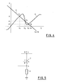
- Many of quantum devices heretofore developed have an I-V characteristic such as the one shown in Figure 4.
- I-V characteristic such as the one shown in Figure 4.
- Figure 5 illustrates an example of a simple positive feedback using a quantum device, in which a quantum device 8 is connected in series to a resistor 7.
- the voltage on this connection point A can be represented by (V o - iR), when the voltage on a point B on the side of the resistor 7 opposite to the quantum device 8 is V o . If the relationship between this voltage and current i is expressed in Figure 4, it will become a straight line 6. This straight line is generally called a load line.
- the axis of abscissas represents a voltage V and the axis of ordinates a current i, and the point of intersection between the load line 6 and the axis of abscissas is V o .
- the voltage-current behavior of the quantum device 8 is shown by a curve 9 in Figure 4. While the points of intersection P 1 , P 2 , and P 3 between the load line 6 and the curve 9 have been shown, the current i flowing through a resistor is aligned with the voltage-current behavior of the quantum device at the voltages and currents indicated by the points, and the positive feedback circuit shown in Figure 5 is stabilized as one system.
- the point A of Figure 5 can express a bit 0 or 1 in correspondence with the voltages V 1 , V 3 according to these two points.
- a positive feedback circuit using the conventional quantum device described above is stabilized at certain voltages V 1 and V 3 , currents i 1 and i 3 corresponding to the voltages always flow in the stabilized state.
- a current that thus flows constantly in a stable state is called a standby current. If heat is generated by the standby current, there will be an important disadvantage that the degree of integration of a circuit is limited. That is, the memory cell using the conventional quantum device has the disadvantage in standby current, because the circuit is not complementary.
- a memory cell which comprises: a plurality of insulating layers; at least three conducting layers spaced with the insulating layers; a first voltage application means for applying a predetermined voltage between first and third conducting layers of the at least three conducting layers, no tunnelling current flowing directly between the first and third conducting layers; and a second voltage application means connected to a second conducting layer of the at least three conducting layers, a tunnelling current being able to flow between the first and second conducting layers and between the second and third conducting layers; wherein quantum-mechanical confinement of free electrons exists in the conducting layers.
- the present invention advantageously provides a memory cell which is structurally simpler than memories being presently used and has positive feedback.
- the present invention also provides a memory cell which has an area equivalent to the cell area of a DRAM and dispenses with a refresh operation.
- the present invention further provides a memory cell with a quantum device.
- a memory cell circuit of the present invention is constituted complementarily and the standby current is reduced greatly.
- FIG. 6 there is shown a preferred embodiment of a memory cell in accordance with the present invention.
- Three conducting layers 20a, 20b, and 20c are spaced with insulating layers 10.
- the quantum-mechanical confinement of free electrons has been made.
- the quantum-mechanical confinement of free electrons used herein is intended to mean that since the motions of free electrons are limited to a very small area, they become in a state of waiting an energy level which is not continuous but discrete.
- the conducting layers are called VDD20a, CL20b, and GND 20c for the sake of convenience.
- a constant voltage is applied by a power supply 24.
- another voltage is applied to CL 20b through a transistor 28 for selection by a bit line BL 25. This transistor 28 is controlled by a word line WL 26.
- the present invention makes use of the phenomenon recently found by the inventors of this application (Y.Katayama, Ph.D.Thesis, Princeton University, June 1994).
- the phenomenon is that:
- the "conducting layer” used herein is referred to as a layer in which free electrons exist at its Fermi level and which, because of that, is in a state where electric conductivity is high.
- the "insulating layer” used herein is referred to as a layer in which, since its Fermi level is located in a band gap, no free electrons exist at the Fermi level and which is in a state where electric conductivity is low.
- These layers can be estimated with their resistivity.
- a conducting layer can be defined as having a resistivity of 1 ohm ⁇ cm or less
- an insulating layer can be defined as having a resistivity of 100 ohm ⁇ cm or more.
- resistivity is an easier method and, physically, they should be discriminated by the above-described definition.
- what is normally called a semiconductor can also be thought of as a conducting layer, if it meets the definition described above.
- the present invention makes use of the phenomenon according to the above-described (a) and (b), but this phenomenon is not well known and is very important for understanding the present invention. Therefore, before describing a preferred embodiment of the present invention in detail, the phenomenon on which the present invention is based will be described.
- This phenomenon makes use of the physical phenomenon of tunnelling between two-dimension electron gases (2DEGs).
- the 2DEG is formed by quantum-mechanically confining free electrons in a certain one-dimensional direction. When this quantum-mechanical confinement is strong, the motion of a free electron will be stated as if it were two-dimensional motion.
- free electrons forming an inverted layer in a channel area is in this state.
- the 2DEG is realized, for example, when an extremely thin conducting layer is formed between insulating layers.
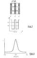
- the inventors employ two GaAs layers (30a, 30b) of thickness about 150 angstroms ( ⁇ ) as a conducting layer, employ three AlAs layers 31 of thickness about 70 ⁇ as insulating layers, and these are alternately stacked.
- the free electrons in these conducting layers are in a 2DEG state and form, quantum wells such as those shown in Figure 7.
- the quantum wells are formed in the conducting layers 30a and 30b, respectively, and two lowest quantum levels are assumed to be E 1 (higher energy) and E 0 (lower energy).
- E 1 higher energy
- E 0 lower energy
- the thickness d c of the conducting layer needs to be sufficiently thin.
- the thickness d c of a conducting layer that presents a 2DEG state can be obtained by the following equations.
- E 1 - E 0 which is a difference between two quantum levels needs to satisfy the following Eq. (5).
- ⁇ h o ⁇ ⁇ E 1 - E 0
- E 1 - E 0 which is a difference between two quantum levels has to be sufficiently greater than the vagueness of a quantum level by scattering
- r h o / ⁇ ( ⁇ is the average scattering time of a free electron). This is because if the vagueness of a quantum level by scattering becomes greater than this energy difference, two energy levels will be continuous and therefore a quantum well will not be formed.
- the upper limit value of d c is determined with m* and ⁇ as parameters.
- m* and ⁇ are material-dependent parameters of a conducting layer substance, and ⁇ also depends upon the temperature of a system, the degree of smoothness of an interface between a conducting layer and an insulating layer, and the concentration of impurities in a conducting layer.
- the thickness d c of a conducting layer is a precondition for carrying out the present invention that the free electrons in the conducting layer are confined in a one-dimensional direction, so in the present invention the thickness of a conducting layer should be determined according to this.
- the magnitude of this tunnelling current i.e., the degree at which free electrons presenting the physical phenomenon of 2DEG are moved to the adjacent conducting layer by the tunnel phenomenon depends upon the thickness d i of an insulating layer defining the extent of the conducting layer.
- the tunnelling current I t is expressed by the following Eq. (7).
- the thickness d i of the insulating layer has the following relationship with t of Eq. (7).
- x 1 and x 2 represent the x-coordinate value normal to one interface of the insulating layer and the x-coordinate value normal to an interface opposing to that one interface, as shown in Figure 7, and d i is equal to x 2 - x i .
- ⁇ 1 represents the density of states in a quantum-mechanical confinement direction
- ⁇ represents the tunnel barrier that an free electron feels.
- m*, ⁇ 1 , and ⁇ what depends on the kind and thickness of an insulating layer substance is m*, ⁇ 1 , and ⁇ . Since this equation performs an integration from x 1 toward x 2 , it cannot be expanded directly with respect to d i . However, if this equation is employed, a person having ordinary skill in the art to which the invention pertains can easily calculate an appropriate insulating layer thickness that can achieve the operation of the present invention.
- the inventors connects this stacked structure, as schematically shown in Figure 8, and a tunnelling current i t flowing between conducting layers was measured with ⁇ V g as a parameter.
- ⁇ V g is 0 when the quantum levels in the conducting layers 30a and 30b are the same, and represents the difference between that state (0) and an applied gate voltage.
- the conducting layers 30a and 30b has been shown in Figure 8, the illustration of the insulating layer 31 is omitted.
- the conducting layer 30a is provided with terminals 33 and 35
- the conducting layer 30b is provided with terminals 34 and 36
- a voltage V ds is applied between the terminals 33 and 34.
- the terminal 35 is connected to ground, the terminal 36 is connected to a current measurement device 37, and a current flowing between conducting layers is measured.
- a metal electrode 32 is provided for adjusting the difference between the quantum levels of two conducting layers 30a and 30b. That is, since the quantum level of the conducting layer 30b changes by applying a variable voltage Vg to the metal electrode 32, the difference of the quantum level with the conducting layer 30a can be varied. Thus, in a system in which electrons are quantum-mechanically confined, the quantum level and the Fermi level of the electron can be changed independently by changing the density of the free electron.
- V ds connected to the conducting layers 30a and 30b represents a voltage of the difference between the Fermi levels of the conducting layers 30a and 30b, and the voltage V g applied to an external metal gate 32 controls the quantum level.
- ⁇ V g is changed, and a change in a current value at that time, i t , is obtained.
- Figure 9 shows this result.
- the axis of abscissas represents a voltage ⁇ V g and the axis of ordinates a current i.
- the conductivity at the peak value of this current is two digits or more greater than the conductivity that is observed in a normal tunnelling phenomenon.
- the memory cell structure according to the present invention comprises three thin conducting layers VDD20a, CL20b, and GND20c spaced with thin insulating layers 10. And, the operation of the memory cell is realized by the structure in which a voltage difference V is applied to the opposite conducting layers, the voltage difference between the conducting layer VDD20a of the first quantum well and the conducting layer GND of the third quantum well is maintained to V, and a voltage is applied to the conducting layer CL20b of the second quantum well through the bit line 25. While it is most preferable that the parallel number of quantum wells be 3, a memory cell can be realized even if 4 or more. As shown in Figure 6, three quantum wells are formed by adopting such structure, and quantum-mechanical confinement of free electrons are made in each quantum well, thereby forming a quantum level.
- each insulating layer and each conducting layer is preferable to be about 50 to 200 ⁇ .
- the principle of the present invention is not limited to such thickness.
- the conducting layers described above may be within a range that meets the requirements of Eqs. (1), (2), and (3), and the insulating layers may be within a range that meets the requirements of Eqs. (4) and (5).
- Figure 10 shows the state in which a voltage has not been applied to the conducting layers VDD20a and GND20c of the opposite quantum wells. In this state a voltage difference has not occurred between the opposite conducting layers. It is now assumed that free electrons sufficiently exist in conducting layers and a Fermi level E f is above the lowest quantum level E 0 and below the next quantum level E 1 . In this state, a tunnelling phenomenon occurs between conducting layers because the insulating layers between the conducting layers are sufficiently thin, and a tunnelling current flows between the conducting layers by the tunnelling phenomenon.
- the reason that the voltage of the quantum level of CL20b in the second quantum well is locked to E 0 is that the tunnelling current between the conducting layer CL20b according to the second quantum well and the conducting layer GND20c according to the third quantum well increases because the voltages of the quantum levels of the conducting layers CL20b and GND20c are close to each other and, on the other hand, the tunnelling current between the conducting layer VDD20a according to the first quantum well and the conducting layer CL20b according to the second quantum well decreases because the voltages of the quantum levels of the conducting layers CL20b and VDD20a are away from each other.
- a tunnelling current and a voltage difference between quantum levels have been described in Figure 9. As a result, the voltage of the conducting layer CL20b comes closer to the conducting layer GND20c, and the voltage of CL is locked to the voltage of GND.
- Figure 14 shows a structure in which single crystal silicon 100 is used as a substrate and layers comprising Si and SiO 2 are laid on the substrate.
- conducting layers GND102, CL104, and VDD106 are formed from Si, and it is preferable that Si be single crystal silicon to reduce the scattering probability of free electrons.
- a SiO 2 layer (not shown) which is an insulating layer is provided around these conducting layers GND102, CL104, and VDD106.
- an electrode WL108 for a transistor for selection may be an arbitrary conductive material. In fabrication step, using the same material as a conducting layer is most advantageous.
- a chemical vapor deposition (CVD) technique can be considered as the first method of fabricating a smooth interface.
- CVD chemical vapor deposition
- the CVD technique when a thin film is formed, it becomes polycrystal or an amorphous state, so there is the problem that the scattering probability of electrons within conducting layers is increased.
- the second method of obtaining a smooth interface there is a method in which oxygen ions are implanted into single crystal silicon, then annealing is performed at high temperature to maintain a single crystal state and also localize oxygen ions, and a Si layer and a SiO 2 layer are alternately formed.
- This method is used in a silicon-on-insulator (SOI) substrate, and it is possible to obtain a very smooth Si-SiO 2 interface (S. Nakajima, presented in JEIDA meeting on Silicon-On-Insulator, Oct 1944).
- Figure 15 shows a structure which, even in a minor way, overcomes the difficulty of obtaining a smooth Si-SiO 2 interface.
- conducting layers VDD116 and GND112 are formed under a conducting layer CL114, and with two layers, this structure is made so that it becomes equivalent to a three-layer structure.
- the arrangement of a single crystal silicon substrate 100 and an electrode WL108 for a transistor for selection is the same as the structure of Figure 14.
- a plane memory cell can also be formed, as shown in Figure 16.
- conducting layers are GND122, CL124, and VDD126, and an electrode WL128 for a transistor for selection is formed so that an insulating layer is interposed between the upper or lower portion of these conducting layers and the electrode WL128.
- an insulating layer 120 is formed between conducting layers there is formed.
- a structure such as this can be formed with a very fine work technique such as an electron beam lithography system.
- the thickness of a conducting layer can be calculated with Eqs. (1), (2), and (3), and the thickness of an insulating layer can be calculated with Eqs. (4) and (5).
- the thickness d c of a Si layer which is a conducting layer can be calculated with Eqs. (1), (2), and (3), and an important parameter is the average scattering time of an free electron, ⁇ .
- ⁇ is largely influenced by the smoothness of the interface between a conducting layer and an insulating layer as well as the kind of a conducting layer substance. If this is supposed from the degree of movement of an electron on a Si-SiO 2 obtained in a MOSFET, ⁇ is about 7.4 x 10 -14 sec. The vagueness of an electron by scattering which is caused by this, ⁇ , is about 0.08 eV. This will satisfy Eq.
- d c becomes thicker, the smoothness on an interface needs to be enhanced to achieve one-dimensional confinement of free electrons, or the structure itself becomes larger and cannot meet the demand of the present invention for miniaturizing a memory cell, so it is preferable that d c be 1000 ⁇ or less.
- the thickness of a SiO 2 which is an insulating layer can be calculated from Eqs. (4) and (5), but the thickness can be extrapolated from experimental results of other materials such as GaAs. From this, a thickness of about 20 to 30 ⁇ will be an optimum value as long as SiO 2 is selected as an insulating layer. For insulating layers, it is a condition that a tunnelling current flows sufficiently, so if within that condition, there is no need of limiting a thickness. It has been found that in GaAs-AlAs system, even 70 ⁇ or so is sufficient.
- the thickness of an insulating layer is determined within this range. Also, if the thickness of an insulating layer becomes too thick, the structure itself will become large and will not meet the demand of the present invention for miniaturizing a memory cell. Therefore, in view of this demand, it is preferable that the thickness be 500 ⁇ or less.
- the equivalent circuit (unit circuit described above) of a 2 parallel quantum wells is shown in Figure 17.
- two quantum levels correspond to the voltages on the points indicated by node S* and node D*.
- This unit circuit is characterized in that S and D representative of a Fermi level are separated by S* and D* representative of a quantum level and by a capacitance C q .
- This capacitance C q represents a quantum capacitance (for Cq, see "S. Luryi, Appl. Phys. Lett. 52, 501 (1988)").
- C w corresponds to a capacitance that an adjacent conducting layer forms
- R t is a resistance as a tunnelling current flows. This R t is equivalent to ⁇ V/I t which is a modification of Eq. (4).
- a constant voltage V ds is applied between nodes S and D and a variable voltage V g is applied.
- the variable voltage V g serves as controlling the voltage difference between S* and D*, E o a - E o b .
- the voltage-current behavior as the terminal on the side of C sub is connected to ground and the variable voltage V g is transitioned, is shown in Figure 18(b).
- the axis of abscissas represents a voltage ⁇ V g and the axis of ordinates represents an observed current value. This behavior accurately corresponds to the behavior of the tunnelling current of the structure of Figure 9 having a 2 parallel quantum wells.
- the unit circuit shown in Figure 17 is formed as an equivalent circuit representative of the voltage-current behavior of a structure having a 2 parallel quantum well. With this, the equivalence between the 2 parallel quantum well structure and the unit circuit, stated in (1), can be verified.
- the equivalent circuit of Figure 19 includes a word line (WL), a bit line (BL), and a FET (TN 1 ) for memory cell selection, to verify the operation of the memory cell. From this structure it will be understood that this equivalent circuit is equivalent to a memory cell which requires a 3 parallel quantum well structure of the present invention. With this, an equivalent circuit of the memory cell of the present invention can be formed, as stated in the above-described (2).
- this equivalent circuit has a characteristic as a memory cell.
- the voltage-current behavior of this equivalent circuit is shown in Figure 20.
- a memory cell according to the present invention is simulated by an equivalent circuit.
- this characteristic is based on a phenomenon in which:
- the present invention is a memory cell with positive feedback. Therefore, it is unnecessary to perform a refresh operation. Also, an essential part of the present invention is constituted with only three conducting layers spaced with insulating layers, so the present invention has a structure simpler than static memories being presently used. An area that this structure occupies depends on a design, but it is substantially equal to the cell area of a DRAM. The present invention forms a memory cell with a quantum device, and since the circuit is complementary, a standby current can greatly be reduced.
Abstract
Description
- The present invention relates to a memory cell, and more particularly to a memory cell for storing information by the use of the quantum mechanical property of free electrons.
- Static memory cells do not require a refresh operation, so they have low power dissipation as compared with dynamic random access memories (DRAMs). The refresh operation is an operation of charging and discharging the capacitance of a DRAM for storing a "0" or "1" as bit information. Such an operation is needed because the capacitance of the DRAM always leaks the stored electric charges from the junction portions, insulating films, and depletion layers.
- Figure 1 shows the structure of a DRAM. Data is stored in a
capacitance 1, the structure of which is shown in Figure 2. That is, aninsulating film 3 is interposed betweenelectrodes 2. Since the miniaturization of memories has recently been required, the distance d between theelectrodes 2 has to be made smaller. If the distance is made smaller, the thickness of theinsulating film 3 will be reduced and the leak current i between the electrodes will easily flow because of that. Such an increase in the leak current means that a refresh operation must frequently be performed. Therefore, as memories are made smaller, the DRAM has the disadvantage that its refresh operation becomes complicated. - As described above, static memory cells do not require a refresh operation. This is due to the structure and operational principle of a static memory cell such as that shown in Figure 3. The outline of this operational principle is as follows: In this static memory cell, two inverters circuits are cross coupled. For example, if a CL terminal is in a high electric potential, and since a CLB terminal goes to the same low electric potential as ground, transistors TN1 and TP2 will be turned on, transistors TN2 and TP1 will be turned off. As a result, the voltage on the CL terminal is maintained high, so this state is stored as information. Since in such a static memory cell this state is maintained by a feedback latch, information will not be lost as long as power is switched off. Therefore, a refresh operation such as a DRAM is not needed and an additional circuit such as a control clock also becomes unnecessary.
- However, even though static memory cell has the above-described advantages, it has the disadvantage that the area occupied by the circuit is large. That is, a feedback circuit for maintaining the voltage levels of circuit terminals is required and a large number of elements for that circuit need to be used, so the chip area is increased. More specifically, while a DRAM is constituted by one capacitor and one transistor for selection, a static memory needs four transistors for a feedback circuit and two transistors for selection as long as it uses a CMOS technique and therefore the area of a cell is very large. This disadvantage is critical in these days when the miniaturization of elements has been desired.
- A device element called a quantum device is being developed in recent years. The quantum device is one which uses the quantum-mechanical property of free electrons to perform information processing. Many of quantum devices heretofore developed have an I-V characteristic such as the one shown in Figure 4. By using the negative differential resistance of this quantum device (characteristic that I is reduced as V is increased), a positive feedback circuit can be constituted with a simpler structure such as that shown in Figure 5.
- The relationship between Figures 4 and 5 will hereinafter be described. Figure 5 illustrates an example of a simple positive feedback using a quantum device, in which a
quantum device 8 is connected in series to aresistor 7. The voltage on this connection point A can be represented by (Vo - iR), when the voltage on a point B on the side of theresistor 7 opposite to thequantum device 8 is Vo. If the relationship between this voltage and current i is expressed in Figure 4, it will become astraight line 6. This straight line is generally called a load line. In Figure 4, the axis of abscissas represents a voltage V and the axis of ordinates a current i, and the point of intersection between theload line 6 and the axis of abscissas is Vo. On the other hand, the voltage-current behavior of thequantum device 8 is shown by acurve 9 in Figure 4. While the points of intersection P1, P2, and P3 between theload line 6 and thecurve 9 have been shown, the current i flowing through a resistor is aligned with the voltage-current behavior of the quantum device at the voltages and currents indicated by the points, and the positive feedback circuit shown in Figure 5 is stabilized as one system. - That is, if two of (i1, V1) according to the point P1 of Figure 4 and (i3, V3) according to the point P3 are considered, a system becomes stable at these two voltage-current conditions and exhibits a positive feedback circuit characteristic. Therefore, the point A of Figure 5 can express a
bit - Since a positive feedback circuit using the conventional quantum device described above is stabilized at certain voltages V1 and V3, currents i1 and i3 corresponding to the voltages always flow in the stabilized state. A current that thus flows constantly in a stable state is called a standby current. If heat is generated by the standby current, there will be an important disadvantage that the degree of integration of a circuit is limited. That is, the memory cell using the conventional quantum device has the disadvantage in standby current, because the circuit is not complementary.
- In accordance with the present invention, there is now provided a memory cell which comprises: a plurality of insulating layers; at least three conducting layers spaced with the insulating layers; a first voltage application means for applying a predetermined voltage between first and third conducting layers of the at least three conducting layers, no tunnelling current flowing directly between the first and third conducting layers; and a second voltage application means connected to a second conducting layer of the at least three conducting layers, a tunnelling current being able to flow between the first and second conducting layers and between the second and third conducting layers; wherein quantum-mechanical confinement of free electrons exists in the conducting layers.
- This advantageously provides a memory cell which is structurally simpler than memories being presently used and has positive feedback. The present invention also provides a memory cell which has an area equivalent to the cell area of a DRAM and dispenses with a refresh operation. The present invention further provides a memory cell with a quantum device. A memory cell circuit of the present invention is constituted complementarily and the standby current is reduced greatly.
- Preferred embodiments of the present invention will now be described with reference to the accompanying drawings in which:
- Figure 1 is a diagram showing the structure of a conventional DRAM;
- Figure 2 is a diagram showing the structure of the capacitance of the conventional DRAM;
- Figure 3 is a diagram showing the structure of a conventional static memory;
- Figure 4 is an I-V characteristic diagram of a quantum device;
- Figure 5 is a diagram showing an example of a conventional quantum device;
- Figure 6 is a diagram showing a memory cell according to the present invention and the energy level thereof;
- Figure 7 is a diagram used to explain the principles of the present invention and showing an energy level;
- Figure 8 is a schematic view showing an experimental circuit used to explain the principles of the present invention;
- Figure 9 is a diagram showing the results of an experiment for explaining the principles of the present invention;
- Figure 10 is a schematic view showing the operation of the present invention;
- Figure 11 is a schematic view showing the operation of the present invention;
- Figure 12 is a schematic view showing the operation of the present invention;
- Figure 13 is a diagram showing the positive feedback of the present invention;
- Figure 14 is a perspective view showing a memory cell according to a first embodiment of the present invention;
- Figure 15 is a perspective view showing a memory cell according to a second embodiment of the present invention;
- Figure 16 is a plan view showing a memory cell according to a third embodiment of the present invention;
- Figure 17 is a diagram showing an simulation circuit for verifying the operation of the principles of the present invention;
- Figure 18 is a diagram showing results obtained by the simulation circuit for verifying the operation of the principles of the present invention;
- Figure 19 is a diagram showing a circuit for simulating a memory cell of the present invention; and
- Figure 20 is a diagram showing results obtained by the circuit for simulating a memory cell of the present invention.
- Referring to Figure 6, there is shown a preferred embodiment of a memory cell in accordance with the present invention. Three conducting
layers layers 10. Within the three conductinglayers GND 20c for the sake of convenience. And, between VDD20a and GND20c, a constant voltage is applied by apower supply 24. Also, another voltage is applied toCL 20b through atransistor 28 for selection by abit line BL 25. Thistransistor 28 is controlled by aword line WL 26. - The present invention makes use of the phenomenon recently found by the inventors of this application (Y.Katayama, Ph.D.Thesis, Princeton University, June 1994). The phenomenon is that:
- (a) When two conducting layers in which free electrons are quantum-mechanically confined in one dimensional direction are spaced with a thin insulating layer,
- (b) If the quantum levels of these two conducting layers come close, a tunnelling current flowing between these two conducting layers through the insulating layer will greatly be increased.
- The "conducting layer" used herein is referred to as a layer in which free electrons exist at its Fermi level and which, because of that, is in a state where electric conductivity is high. Also, the "insulating layer" used herein is referred to as a layer in which, since its Fermi level is located in a band gap, no free electrons exist at the Fermi level and which is in a state where electric conductivity is low. These layers can be estimated with their resistivity. For example, a conducting layer can be defined as having a resistivity of 1 ohm·cm or less, and an insulating layer can be defined as having a resistivity of 100 ohm·cm or more. However, the definition by resistivity is an easier method and, physically, they should be discriminated by the above-described definition. In the present invention, what is normally called a semiconductor can also be thought of as a conducting layer, if it meets the definition described above.
- The present invention makes use of the phenomenon according to the above-described (a) and (b), but this phenomenon is not well known and is very important for understanding the present invention. Therefore, before describing a preferred embodiment of the present invention in detail, the phenomenon on which the present invention is based will be described.
- This phenomenon makes use of the physical phenomenon of tunnelling between two-dimension electron gases (2DEGs). The 2DEG is formed by quantum-mechanically confining free electrons in a certain one-dimensional direction. When this quantum-mechanical confinement is strong, the motion of a free electron will be stated as if it were two-dimensional motion. As a concrete example, in a MOS transistor, free electrons forming an inverted layer in a channel area is in this state.
- This phenomenon is confirmed by measuring a tunnelling current flowing between conducting layers in a GaAs-AlAs quantum well structure by a 4-terminal method. The outline of this discovery will hereinafter be stated.
- The 2DEG is realized, for example, when an extremely thin conducting layer is formed between insulating layers. As shown in Figure 7, the inventors employ two GaAs layers (30a, 30b) of thickness about 150 angstroms (Å) as a conducting layer, employ three AlAs
layers 31 of thickness about 70 Å as insulating layers, and these are alternately stacked. - The free electrons in these conducting layers are in a 2DEG state and form, quantum wells such as those shown in Figure 7. Now, the quantum wells are formed in the conducting layers 30a and 30b, respectively, and two lowest quantum levels are assumed to be E1 (higher energy) and E0 (lower energy). Thus, in order to present a 2DEG state, discontinuity needs to occur between the quantum levels by confining free electrons in a one-dimensional direction. And, for that, the thickness dc of the conducting layer needs to be sufficiently thin. The thickness dc of a conducting layer that presents a 2DEG state can be obtained by the following equations. First, the relationship between the thickness dc of the conducting layer and two lowest quantum levels E0, E1 is given by the following Eq. 4.

- Also, as a condition under which 2DEG is formed and the quantum-mechanical confinement of free electrons is made, E1 - E0 which is a difference between two quantum levels needs to satisfy the following Eq. (5).

- That is, E1 - E0 which is a difference between two quantum levels has to be sufficiently greater than the vagueness of a quantum level by scattering, r = ho/τ (τ is the average scattering time of a free electron). This is because if the vagueness of a quantum level by scattering becomes greater than this energy difference, two energy levels will be continuous and therefore a quantum well will not be formed.
- If both Eqs. (4) and (5) are expanded with respect to the thickness dc, finally the following Eq. (6) will be obtained.

- Therefore, the upper limit value of dc is determined with m* and τ as parameters.
- Now, m* and τ are material-dependent parameters of a conducting layer substance, and τ also depends upon the temperature of a system, the degree of smoothness of an interface between a conducting layer and an insulating layer, and the concentration of impurities in a conducting layer.
- The thickness dc of a conducting layer is a precondition for carrying out the present invention that the free electrons in the conducting layer are confined in a one-dimensional direction, so in the present invention the thickness of a conducting layer should be determined according to this.
- Next, in order to realize this phenomenon that the present invention uses, it is necessary that a sufficient tunnelling current flows between the conducting
layers 
- Also, the thickness di of the insulating layer has the following relationship with t of Eq. (7).

- In Eq. (8), x1 and x2 represent the x-coordinate value normal to one interface of the insulating layer and the x-coordinate value normal to an interface opposing to that one interface, as shown in Figure 7, and di is equal to x2 - xi. Also, ρ1 represents the density of states in a quantum-mechanical confinement direction, and Δϕ represents the tunnel barrier that an free electron feels. Among these, what depends on the kind and thickness of an insulating layer substance is m*, ρ1, and Δϕ. Since this equation performs an integration from x1 toward x2, it cannot be expanded directly with respect to di. However, if this equation is employed, a person having ordinary skill in the art to which the invention pertains can easily calculate an appropriate insulating layer thickness that can achieve the operation of the present invention.
- The inventors connects this stacked structure, as schematically shown in Figure 8, and a tunnelling current it flowing between conducting layers was measured with ΔVg as a parameter. ΔVg is 0 when the quantum levels in the conducting layers 30a and 30b are the same, and represents the difference between that state (0) and an applied gate voltage. Note that while the conducting layers 30a and 30b has been shown in Figure 8, the illustration of the insulating
layer 31 is omitted. And, theconducting layer 30a is provided withterminals conducting layer 30b is provided withterminals terminals current measurement device 37, and a current flowing between conducting layers is measured. Ametal electrode 32 is provided for adjusting the difference between the quantum levels of two conductinglayers conducting layer 30b changes by applying a variable voltage Vg to themetal electrode 32, the difference of the quantum level with theconducting layer 30a can be varied. Thus, in a system in which electrons are quantum-mechanically confined, the quantum level and the Fermi level of the electron can be changed independently by changing the density of the free electron. In Figure 8, Vds connected to the conducting layers 30a and 30b represents a voltage of the difference between the Fermi levels of the conducting layers 30a and 30b, and the voltage Vg applied to anexternal metal gate 32 controls the quantum level. In measurements, ΔVg is changed, and a change in a current value at that time, it, is obtained. - Figure 9 shows this result. In the figure, the axis of abscissas represents a voltage ΔVg and the axis of ordinates a current i. When the difference of the quantum level is the same (i.e., ΔVg = 0), there is the remarkable tendency that the maximum current flows. And, the conductivity at the peak value of this current is two digits or more greater than the conductivity that is observed in a normal tunnelling phenomenon. From this experiment, the inventors have found that (1) in a case where the physical phenomenon of 2DEG occurs and layers in which electrons are quantum-mechanically confined in one direction are adjacent through an insulating layer, (2) if the quantum levels of these adjacent layers come close, a very large current will flow as compared with a normal tunnelling current or a value of resistance will become extremely small as compared with a normal tunnelling resistance.
- It is noted that in GaAs-AlAs system in which the inventors have confirmed the phenomenon described above, this phenomenon was confirmed at very low temperature. However, this is because the band gap of AlAs as an insulating layer is small and therefore the height of the barrier of a quantum well is insufficient, and is not an essential problem. That is, in a case where the barrier height of the quantum well is insufficient, since the value of the difference (E1 - E0) between quantum levels of electrons by quantum confinement is not large. If the temperature becomes higher a width will occur in respective quantum levels and both levels will be continuous, so quantum confinement in a one-dimensional direction is broken. Therefore, with an insulating material where its band gap is large, such as SiO2, the above-described phenomenon can be observed at high temperature, for example, room temperature.
- The memory cell according to the present invention is again shown in Figure 6. As shown, the memory cell structure according to the present invention comprises three thin conducting layers VDD20a, CL20b, and GND20c spaced with thin insulating layers 10. And, the operation of the memory cell is realized by the structure in which a voltage difference V is applied to the opposite conducting layers, the voltage difference between the conducting layer VDD20a of the first quantum well and the conducting layer GND of the third quantum well is maintained to V, and a voltage is applied to the conducting layer CL20b of the second quantum well through the
bit line 25. While it is most preferable that the parallel number of quantum wells be 3, a memory cell can be realized even if 4 or more. As shown in Figure 6, three quantum wells are formed by adopting such structure, and quantum-mechanical confinement of free electrons are made in each quantum well, thereby forming a quantum level. - The thickness of each insulating layer and each conducting layer is preferable to be about 50 to 200 Å. However, the principle of the present invention is not limited to such thickness. The conducting layers described above may be within a range that meets the requirements of Eqs. (1), (2), and (3), and the insulating layers may be within a range that meets the requirements of Eqs. (4) and (5).
- The operational principle of this structure will be described with reference to Figures 10 to 12. Figure 10 shows the state in which a voltage has not been applied to the conducting layers VDD20a and GND20c of the opposite quantum wells. In this state a voltage difference has not occurred between the opposite conducting layers. It is now assumed that free electrons sufficiently exist in conducting layers and a Fermi level Ef is above the lowest quantum level E0 and below the next quantum level E1. In this state, a tunnelling phenomenon occurs between conducting layers because the insulating layers between the conducting layers are sufficiently thin, and a tunnelling current flows between the conducting layers by the tunnelling phenomenon.
- Next, the state in which a voltage V has been applied to the opposite conducting layers VDD20a and GND20c of this system is shown in Figure 11. If a normal system, the quantum level of the conducting layer CL20b in the second quantum well is to be maintained between E0 and E0'. However, in the structure according to the present invention, since the degree of freedom of free electrons has been reduced by the above-described 2DEG phenomenon, the quantum level of the conducting layer CL20b in the second quantum well is locked to the voltage of E0 or E0.. In Figure 11 the voltage of the quantum level of CL20b has been locked to E0 equal to the voltage of the quantum level of the GND20c, and this corresponds to a "0" in a binary state. The reason that the voltage of the quantum level of CL20b in the second quantum well is locked to E0 is that the tunnelling current between the conducting layer CL20b according to the second quantum well and the conducting layer GND20c according to the third quantum well increases because the voltages of the quantum levels of the conducting layers CL20b and GND20c are close to each other and, on the other hand, the tunnelling current between the conducting layer VDD20a according to the first quantum well and the conducting layer CL20b according to the second quantum well decreases because the voltages of the quantum levels of the conducting layers CL20b and VDD20a are away from each other. Note that a tunnelling current and a voltage difference between quantum levels have been described in Figure 9. As a result, the voltage of the conducting layer CL20b comes closer to the conducting layer GND20c, and the voltage of CL is locked to the voltage of GND.
- Next, when the conducting layer CL20b is slightly transitioned to the side of the voltage of the conducting layer VDD20a, the voltage of the conducting layer CL20b and the voltage of the conducting layer GND20c are away from each other, so the tunnelling current between the conducting layer CL20b and the conducting layer GND20c decreases, and instead, the voltage of the conducting layer CL20b and the voltage of the conducting layer VDD20a come close, so the tunnelling current between the conducting layer CL20b and the conducting layer VDD20a increases. With this, the conducting layers CL20b and VDD20a are transitioned so that their voltages come close to each other. This state is shown in Figure 12. And, this state corresponds to a "1" in a binary state.
- The relationship between the voltage of the conducting layer CL operating as a memory cell of the present invention and the stability thereof is schematically shown in Figure 13. From this figure it follows that in an initial state (Figure 10) where the voltage of CL is between the voltages of VDD and GND, the voltage of CL is extremely unstable and, if this comes closer to either of VDD and GND, the voltage of CL will be stabilized. That is, in the initial state the voltage of the second conducting layer is in an extremely unstable state and is in a state of waiting application of a voltage either toward GND or VDD. And, if once this is applied, the voltage of CL will acceleratedly shift toward a stable state (GND voltage or VDD voltage). Because of this characteristic, the memory cell according to the present invention has positive feedback.
- Next, the operations as reading and writing of information are performed with this memory cell will be described. In Figure 6, when information is read out of this memory cell, a
FET 28 is turned on and thebit line 25 is driven with the positive feedback of the memory cell. Also, information writing can be performed by forcibly changing the voltage of CL by thebit line 25. If theFET 28 is turned off, the memory cell will be disconnected from an external circuit, and as long as an external supply voltage is applied, information will be maintained by the positive feedback. - Some examples of a structure actually using this three-layer structure are shown. Figure 14 shows a structure in which
single crystal silicon 100 is used as a substrate and layers comprising Si and SiO2 are laid on the substrate. In Figure 14, conducting layers GND102, CL104, and VDD106 are formed from Si, and it is preferable that Si be single crystal silicon to reduce the scattering probability of free electrons. Also, a SiO2 layer (not shown) which is an insulating layer is provided around these conducting layers GND102, CL104, and VDD106. Also, an electrode WL108 for a transistor for selection may be an arbitrary conductive material. In fabrication step, using the same material as a conducting layer is most advantageous. - What is important in the structure of the present invention is an interface between Si and SiO2. If this interface is not sufficiently smooth, the scattering probability of free electrons will become higher and therefore confinement of free electrons cannot be achieved. A chemical vapor deposition (CVD) technique can be considered as the first method of fabricating a smooth interface. However, in the CVD technique, when a thin film is formed, it becomes polycrystal or an amorphous state, so there is the problem that the scattering probability of electrons within conducting layers is increased.
- Also, as the second method of obtaining a smooth interface, there is a method in which oxygen ions are implanted into single crystal silicon, then annealing is performed at high temperature to maintain a single crystal state and also localize oxygen ions, and a Si layer and a SiO2 layer are alternately formed. This method is used in a silicon-on-insulator (SOI) substrate, and it is possible to obtain a very smooth Si-SiO2 interface (S. Nakajima, presented in JEIDA meeting on Silicon-On-Insulator, Oct 1944).
- Figure 15 shows a structure which, even in a minor way, overcomes the difficulty of obtaining a smooth Si-SiO2 interface. In this structure, conducting layers VDD116 and GND112 are formed under a conducting layer CL114, and with two layers, this structure is made so that it becomes equivalent to a three-layer structure. The arrangement of a single
crystal silicon substrate 100 and an electrode WL108 for a transistor for selection is the same as the structure of Figure 14. - Further, a plane memory cell can also be formed, as shown in Figure 16. In this memory cell, conducting layers are GND122, CL124, and VDD126, and an electrode WL128 for a transistor for selection is formed so that an insulating layer is interposed between the upper or lower portion of these conducting layers and the electrode WL128. Also, between conducting layers there is formed an insulating
layer 120. A structure such as this can be formed with a very fine work technique such as an electron beam lithography system. - When Si-SiO2 system is employed, the thickness of a conducting layer can be calculated with Eqs. (1), (2), and (3), and the thickness of an insulating layer can be calculated with Eqs. (4) and (5).
- For example, the thickness dc of a Si layer which is a conducting layer can be calculated with Eqs. (1), (2), and (3), and an important parameter is the average scattering time of an free electron, τ. τ is largely influenced by the smoothness of the interface between a conducting layer and an insulating layer as well as the kind of a conducting layer substance. If this is supposed from the degree of movement of an electron on a Si-SiO2 obtained in a MOSFET, τ is about 7.4 x 10⁻¹⁴ sec. The vagueness of an electron by scattering which is caused by this, Γ, is about 0.08 eV. This will satisfy Eq. (2) if it is assumed that the difference between two quantum levels of a conducting layer, E1 - E0 is 0.1 eV. If these are premised on and Eq. (3) is calculated by substituting the effective mass of a free electron, m* = 0.26 m, the thickness dc will be less than about 60 Å. However, since this value is largely influenced by τ which is influenced by the smoothness of a Si-SiO2 interface, the thickness dc may be a little thicker if smoothness can further be enhanced. In GaAs-AlAs system the interface can actually be smoothed sufficiently. Therefore, particularly at low temperature, one-dimensional confinement of free electrons is possible even in a further thick layer (for example, 100 to 200 Å). However, as dc becomes thicker, the smoothness on an interface needs to be enhanced to achieve one-dimensional confinement of free electrons, or the structure itself becomes larger and cannot meet the demand of the present invention for miniaturizing a memory cell, so it is preferable that dc be 1000 Å or less.
- Also, the thickness of a SiO2 which is an insulating layer can be calculated from Eqs. (4) and (5), but the thickness can be extrapolated from experimental results of other materials such as GaAs. From this, a thickness of about 20 to 30 Å will be an optimum value as long as SiO2 is selected as an insulating layer. For insulating layers, it is a condition that a tunnelling current flows sufficiently, so if within that condition, there is no need of limiting a thickness. It has been found that in GaAs-AlAs system, even 70 Å or so is sufficient. A tunnelling current value (per unit area) that should flow, It, can be calculated by It = CV/τ where C represents the capacitance between conducting layers, τ represents a time for charging the capacitance, and V is the voltage applied to the capacitance. For example, if C = 10-7 F/cm2, V = 1 V, and τ = 10-9 sec, Itz is about 100 Å/cm2. Thus, It depends on how fast a memory cell is operated, so it is not determined physically but is a matter of design. However, since the access speed of a current DRAM is about 7 x 10⁻⁸ sec, setting It to less than 1 Å/cm2 lacks actuality. Therefore, it is practical that the thickness of an insulating layer is determined within this range. Also, if the thickness of an insulating layer becomes too thick, the structure itself will become large and will not meet the demand of the present invention for miniaturizing a memory cell. Therefore, in view of this demand, it is preferable that the thickness be 500 Å or less.
- The possibility of realization of the memory cell proposed by the present invention will be verified with a simulation model. As this verification, (1) there is shown a circuit (unit circuit) equivalent to the above-described structure having a 2-parallel quantum wells, (2) an equivalent circuit of a memory cell having a 3 parallel quantum well according to the present invention is formed by combining the unit circuits, and (3) the results obtained as a characteristic as a memory cell is simulated with the equivalent circuit will be described. That is, the equivalence between the 2 parallel quantum well structure and the unit circuit is verified by (1). The equivalence between the equivalent circuit comprising a combination of unit circuits and the memory cell using a 3 parallel quantum well according to the present invention is verified by (2). It is verified by (3) that the equivalent circuit exhibits the characteristic or positive feedback of the memory cell.
- The above-described (1) is disclosed in "Lumped Circuit Model of Two-Dimensional to Two-Dimensional tunnelling transistor, Y. Katayama, D.C. Tsui, Appl. Phys. Lett 62(20), 17 May 1993." The outline of the contents of this literature will hereinafter be described.
- According to this, the equivalent circuit (unit circuit described above) of a 2 parallel quantum wells is shown in Figure 17. In the unit circuit, two quantum levels correspond to the voltages on the points indicated by node S* and node D*. This unit circuit, as compared with the equivalent circuit of a conventional transistor, is characterized in that S and D representative of a Fermi level are separated by S* and D* representative of a quantum level and by a capacitance Cq. This capacitance Cq represents a quantum capacitance (for Cq, see "S. Luryi, Appl. Phys. Lett. 52, 501 (1988)"). Also, Cw corresponds to a capacitance that an adjacent conducting layer forms, and Rt is a resistance as a tunnelling current flows. This Rt is equivalent to ΔV/It which is a modification of Eq. (4).
- As shown in Figure 18, in the unit circuit, a constant voltage Vds is applied between nodes S and D and a variable voltage Vg is applied. The variable voltage Vg serves as controlling the voltage difference between S* and D*, Eo a - Eo b. The voltage-current behavior as the terminal on the side of Csub is connected to ground and the variable voltage Vg is transitioned, is shown in Figure 18(b). In the figure, the axis of abscissas represents a voltage ΔVg and the axis of ordinates represents an observed current value. This behavior accurately corresponds to the behavior of the tunnelling current of the structure of Figure 9 having a 2 parallel quantum wells. Therefore, it follows that the unit circuit shown in Figure 17 is formed as an equivalent circuit representative of the voltage-current behavior of a structure having a 2 parallel quantum well. With this, the equivalence between the 2 parallel quantum well structure and the unit circuit, stated in (1), can be verified.
- Next, the equivalence between an equivalent circuit of a memory cell of the present invention comprising a combination of unit circuits and an actual 3 parallel quantum well structure, stated in (2), will be described. If it is assumed that a unit circuit is equivalent to a 2 parallel quantum well structure, a 3 parallel quantum well structure will be equal to a structure in which two unit circuits representative of a 2 parallel quantum well structure are arranged, as shown in Figure 19. In the figure, Cw1 corresponds to the capacitance between conducting layers VDD and CL, and Cw2 corresponds to the capacitance between conducting layers CL and GND. Rt1 corresponds to the tunnelling resistance between conducting layers VDD and CL, and Rt2 corresponds to the tunnelling resistance between conducting layers CL and GND. Therefore, it is understood that a circuit (Figure 19) in which two unit circuits are coupled at node CL* is an equivalent of a 3 parallel quantum well structure such as that shown in Figure 6. Now, when the circuit of Figure 19 is compared with the unit circuit according to Figure 17, Cg is removed. In the unit circuit the Cg is needed because a gate voltage is applied based on the object of the experiment, while in the equivalent circuit the Cg is not needed because a gate voltage is not applied. Therefore, even if Cg is not shown, the equivalence between circuits will not be lost.
- Also, the equivalent circuit of Figure 19 includes a word line (WL), a bit line (BL), and a FET (TN1) for memory cell selection, to verify the operation of the memory cell. From this structure it will be understood that this equivalent circuit is equivalent to a memory cell which requires a 3 parallel quantum well structure of the present invention. With this, an equivalent circuit of the memory cell of the present invention can be formed, as stated in the above-described (2).
- Finally, it will be described that, as stated in (3), this equivalent circuit has a characteristic as a memory cell. The voltage-current behavior of this equivalent circuit is shown in Figure 20. A memory cell according to the present invention is simulated by an equivalent circuit. In Figure 20, there is shown the behavior of CL as BL changes according to 1 = > 0 = > 1 = > 0. Since WL performs a bias operation for switching (Figure 6), TN1 is turned on when WL is high, so the voltage of CL becomes equal to the voltage of BL. And, since TN1 is turned off when WL goes to low, if it is assumed that the memory cell of the present invention has positive feedback, the voltage of CL will continue to transition toward a certain stable voltage and, finally, it is to be held in a stable voltage state.
- The foregoing description is exactly verified by the results of the simulation. That is, if BL is in a high state between t1 and t3 and WL is turned on between t1 and t2, CL will indicate V1 after a slight transition time. At this time, the voltage of CL continues to rise even after WL is turned off (t2), and finally, the voltage of CL is stabilized at t2'. It is a verification of positive feedback that the transition of CL toward a stable state continues after TN1 is turned off. Therefore, it is understood that the equivalent circuit has the characteristic of a memory cell, as stated in (3), and particularly, it has positive feedback which is the characteristic of a static memory. From the verification of (1), (2), and (3), the realization of the present invention can be verified.
- And, from the standpoint of the quantum behavior of electrons, this characteristic is based on a phenomenon in which:
- (a) When two conducting layers in which free electrons have quantum-mechanically been confined in a one-dimensional direction are spaced with a thin insulating layer,
- (b) If the quantum levels of the two conducting layers come close, a tunnelling current flowing between the conducting layers through the insulating layer will be greatly increased.
- That is, since this phenomenon is used, when the energy level of the second quantum well moves toward the level of the first or third quantum well having an energy level close to that energy level, a tunnelling current between the second quantum well and the quantum well having an energy level close to the second quantum well increases greatly, so the energy level of the second quantum well moves in the direction where the voltage difference between two quantum wells is reduced, and is stabilized. This is the reason why the present invention can obtain positive feedback.
- The present invention is a memory cell with positive feedback. Therefore, it is unnecessary to perform a refresh operation. Also, an essential part of the present invention is constituted with only three conducting layers spaced with insulating layers, so the present invention has a structure simpler than static memories being presently used. An area that this structure occupies depends on a design, but it is substantially equal to the cell area of a DRAM. The present invention forms a memory cell with a quantum device, and since the circuit is complementary, a standby current can greatly be reduced.
Claims (14)
- A memory cell comprising:a plurality of insulating layers;at least three conducting layers spaced with the insulating layers;a first voltage application means for applying a predetermined voltage between first and third conducting layers of the at least three conducting layers, no tunnelling current flowing directly between the first and third conducting layers; anda second voltage application means connected to a second conducting layer of the at least three conducting layers, a tunnelling current being able to flow between the first and second conducting layers and between the second and third conducting layers;quantum-mechanical confinement of free electrons having been made to the at least three conducting layers.
- A memory cell as claimed in Claim 1, wherein the second voltage application means includes an interrupting switch.
- A memory cell as claimed in Claim 1, wherein information is stored in correspondence with the potential of the second conducting layer that is controlled by the second voltage application means.
- A memory cell as claimed in Claim 1, wherein the second voltage application means applies two predetermined voltages to the conducting layer.
- A memory cell as claimed in Claim 1, wherein the voltage of the second conducting layer becomes stable at the voltage of the first conducting layer or the voltage of the third conducting layer, and has positive feedback.
- A memory cell as claimed in Claim 1, wherein a thickness of the conducting layers, dc, is given by equation (1),

- A memory cell as claimed in Claim 1, wherein a thickness of the conducting layers, dc, is 1000 Å or less.
- A memory cell as claimed in Claim 1, wherein a thickness of the insulating layers, di, includes a range that can be determined according to di = x2 - x1 as the maximum obtained by equation (2) and equation (3), It, is greater than or equal to 1 A/cm2, the equations (2) and (3) being given by


- A memory cell as claimed in Claim 1, wherein a thickness of the insulating layers, di, is 500 Å or less.
- A memory cell as claimed in Claim 1, wherein the conducting layers comprise silicon (Si) and the insulating layers comprise silicon oxide (SiO2).
- A memory cell as claimed in Claim 1, wherein the resistivity of the conducting layers is 1 ohm·cm or less.
- A memory cell as claimed in Claim 1, wherein free electrons exist in the Fermi level of the conducting layers.
- A memory cell as claimed in Claim 1, wherein the resistivity of the insulating layers is at least 100 ohm·cm or more.
- A memory cell as claimed in Claim 1, wherein no free electrons exist in the Fermi level of the insulating layers.
Applications Claiming Priority (3)
| Application Number | Priority Date | Filing Date | Title |
|---|---|---|---|
| JP33998/95 | 1995-02-22 | ||
| JP7033998A JP2986057B2 (en) | 1995-02-22 | 1995-02-22 | Memory cell |
| JP3399895 | 1995-02-22 |
Publications (3)
| Publication Number | Publication Date |
|---|---|
| EP0729156A2 true EP0729156A2 (en) | 1996-08-28 |
| EP0729156A3 EP0729156A3 (en) | 1999-07-28 |
| EP0729156B1 EP0729156B1 (en) | 2001-12-19 |
Family
ID=12402137
Family Applications (1)
| Application Number | Title | Priority Date | Filing Date |
|---|---|---|---|
| EP96300716A Expired - Lifetime EP0729156B1 (en) | 1995-02-22 | 1996-02-01 | Memory cell |
Country Status (8)
| Country | Link |
|---|---|
| US (1) | US5625589A (en) |
| EP (1) | EP0729156B1 (en) |
| JP (1) | JP2986057B2 (en) |
| KR (1) | KR0184629B1 (en) |
| AT (1) | ATE211295T1 (en) |
| DE (1) | DE69618044T2 (en) |
| ES (1) | ES2167515T3 (en) |
| TW (1) | TW270995B (en) |
Families Citing this family (2)
| Publication number | Priority date | Publication date | Assignee | Title |
|---|---|---|---|---|
| EP0797182A1 (en) * | 1996-03-19 | 1997-09-24 | Hitachi, Ltd. | Active matrix LCD with data holding circuit in each pixel |
| US7534710B2 (en) * | 2005-12-22 | 2009-05-19 | International Business Machines Corporation | Coupled quantum well devices (CQWD) containing two or more direct selective contacts and methods of making same |
Citations (3)
| Publication number | Priority date | Publication date | Assignee | Title |
|---|---|---|---|---|
| EP0225698A1 (en) * | 1985-10-12 | 1987-06-16 | Fujitsu Limited | Logic circuitry |
| US5023836A (en) * | 1988-07-20 | 1991-06-11 | Fujitsu Limited | Semiconductor memory device |
| US5390145A (en) * | 1993-04-15 | 1995-02-14 | Fujitsu Limited | Resonance tunnel diode memory |
Family Cites Families (3)
| Publication number | Priority date | Publication date | Assignee | Title |
|---|---|---|---|---|
| US5251170A (en) * | 1991-11-04 | 1993-10-05 | Nonvolatile Electronics, Incorporated | Offset magnetoresistive memory structures |
| JPH05190922A (en) * | 1992-01-09 | 1993-07-30 | Hitachi Ltd | Quantum storage device |
| US5420819A (en) * | 1992-09-24 | 1995-05-30 | Nonvolatile Electronics, Incorporated | Method for sensing data in a magnetoresistive memory using large fractions of memory cell films for data storage |
-
1995
- 1995-02-22 JP JP7033998A patent/JP2986057B2/en not_active Expired - Fee Related
- 1995-07-24 TW TW084107637A patent/TW270995B/en active
- 1995-12-28 KR KR1019950061413A patent/KR0184629B1/en not_active IP Right Cessation
-
1996
- 1996-02-01 AT AT96300716T patent/ATE211295T1/en not_active IP Right Cessation
- 1996-02-01 EP EP96300716A patent/EP0729156B1/en not_active Expired - Lifetime
- 1996-02-01 ES ES96300716T patent/ES2167515T3/en not_active Expired - Lifetime
- 1996-02-01 DE DE69618044T patent/DE69618044T2/en not_active Expired - Fee Related
- 1996-02-22 US US08/605,564 patent/US5625589A/en not_active Expired - Fee Related
Patent Citations (3)
| Publication number | Priority date | Publication date | Assignee | Title |
|---|---|---|---|---|
| EP0225698A1 (en) * | 1985-10-12 | 1987-06-16 | Fujitsu Limited | Logic circuitry |
| US5023836A (en) * | 1988-07-20 | 1991-06-11 | Fujitsu Limited | Semiconductor memory device |
| US5390145A (en) * | 1993-04-15 | 1995-02-14 | Fujitsu Limited | Resonance tunnel diode memory |
Also Published As
| Publication number | Publication date |
|---|---|
| US5625589A (en) | 1997-04-29 |
| TW270995B (en) | 1996-02-21 |
| EP0729156B1 (en) | 2001-12-19 |
| DE69618044D1 (en) | 2002-01-31 |
| DE69618044T2 (en) | 2002-08-29 |
| JP2986057B2 (en) | 1999-12-06 |
| KR0184629B1 (en) | 1999-03-20 |
| JPH08250672A (en) | 1996-09-27 |
| KR960032764A (en) | 1996-09-17 |
| ATE211295T1 (en) | 2002-01-15 |
| EP0729156A3 (en) | 1999-07-28 |
| ES2167515T3 (en) | 2002-05-16 |
Similar Documents
| Publication | Publication Date | Title |
|---|---|---|
| CN110192279B (en) | Memory cell and method of forming capacitor | |
| US7239542B2 (en) | Storage apparatus | |
| US9336858B2 (en) | Semiconductor memory device and driving method thereof | |
| US5883829A (en) | Memory cell having negative differential resistance devices | |
| King et al. | Charge-trap memory device fabricated by oxidation of si/sub 1-x/ge/sub x | |
| JP3613594B2 (en) | Semiconductor element and semiconductor memory device using the same | |
| Terauchi et al. | A surrounding gate transistor (SGT) gain cell for ultra high density DRAMs | |
| EP0253631B1 (en) | Semiconductor memory device | |
| TWI779309B (en) | Memory cells and methods of forming a capacitor including current leakage paths having different total resistances | |
| CN1211827A (en) | Ferroelectric memory transistor with resistively couple floating gate | |
| US5677637A (en) | Logic device using single electron coulomb blockade techniques | |
| US20060022248A1 (en) | Electronic data memory device for a high read current | |
| KR100715635B1 (en) | Capacitor loaded memory cell | |
| EP0674798B1 (en) | Memory device | |
| US5844834A (en) | Single-electron memory cell configuration | |
| EP0729156B1 (en) | Memory cell | |
| Zhou et al. | Inversion-type ferroelectric capacitive memory and its 1-kbit crossbar array | |
| KR100389969B1 (en) | Nonlinear devices and bistable memory devices | |
| US11508426B1 (en) | Memory device, memory cell arrangement, and methods thereof | |
| GB2362990A (en) | Memory device having p- and n-channel ferroelectric transistors | |
| Katayama et al. | Design and analysis of high-speed random access memory with coulomb blockade charge confinement | |
| JPS58118090A (en) | Memory device | |
| US6251713B1 (en) | Method of making an SRAM storage cell with N channel thin film transistor load devices | |
| US11737375B2 (en) | Device including elements for compensating for local variability of electrostatic potential | |
| GB1597725A (en) | Integrated circuit memory |
Legal Events
| Date | Code | Title | Description |
|---|---|---|---|
| PUAI | Public reference made under article 153(3) epc to a published international application that has entered the european phase |
Free format text: ORIGINAL CODE: 0009012 |
|
| AK | Designated contracting states |
Kind code of ref document: A2 Designated state(s): AT BE CH DE ES FR GB IT LI NL SE |
|
| 17P | Request for examination filed |
Effective date: 19970120 |
|
| PUAL | Search report despatched |
Free format text: ORIGINAL CODE: 0009013 |
|
| AK | Designated contracting states |
Kind code of ref document: A3 Designated state(s): AT BE CH DE ES FR GB IT LI NL SE |
|
| RIC1 | Information provided on ipc code assigned before grant |
Free format text: 6G 11C 11/38 A, 6G 11C 11/34 B |
|
| GRAG | Despatch of communication of intention to grant |
Free format text: ORIGINAL CODE: EPIDOS AGRA |
|
| 17Q | First examination report despatched |
Effective date: 20010308 |
|
| GRAG | Despatch of communication of intention to grant |
Free format text: ORIGINAL CODE: EPIDOS AGRA |
|
| GRAH | Despatch of communication of intention to grant a patent |
Free format text: ORIGINAL CODE: EPIDOS IGRA |
|
| GRAH | Despatch of communication of intention to grant a patent |
Free format text: ORIGINAL CODE: EPIDOS IGRA |
|
| GRAA | (expected) grant |
Free format text: ORIGINAL CODE: 0009210 |
|
| AK | Designated contracting states |
Kind code of ref document: B1 Designated state(s): AT BE CH DE ES FR GB IT LI NL SE |
|
| PG25 | Lapsed in a contracting state [announced via postgrant information from national office to epo] |
Ref country code: LI Free format text: LAPSE BECAUSE OF FAILURE TO SUBMIT A TRANSLATION OF THE DESCRIPTION OR TO PAY THE FEE WITHIN THE PRESCRIBED TIME-LIMIT Effective date: 20011219 Ref country code: CH Free format text: LAPSE BECAUSE OF FAILURE TO SUBMIT A TRANSLATION OF THE DESCRIPTION OR TO PAY THE FEE WITHIN THE PRESCRIBED TIME-LIMIT Effective date: 20011219 Ref country code: BE Free format text: LAPSE BECAUSE OF FAILURE TO SUBMIT A TRANSLATION OF THE DESCRIPTION OR TO PAY THE FEE WITHIN THE PRESCRIBED TIME-LIMIT Effective date: 20011219 Ref country code: AT Free format text: LAPSE BECAUSE OF FAILURE TO SUBMIT A TRANSLATION OF THE DESCRIPTION OR TO PAY THE FEE WITHIN THE PRESCRIBED TIME-LIMIT Effective date: 20011219 |
|
| REF | Corresponds to: |
Ref document number: 211295 Country of ref document: AT Date of ref document: 20020115 Kind code of ref document: T |
|
| REG | Reference to a national code |
Ref country code: CH Ref legal event code: EP |
|
| REG | Reference to a national code |
Ref country code: GB Ref legal event code: IF02 |
|
| REF | Corresponds to: |
Ref document number: 69618044 Country of ref document: DE Date of ref document: 20020131 |
|
| PGFP | Annual fee paid to national office [announced via postgrant information from national office to epo] |
Ref country code: FR Payment date: 20020219 Year of fee payment: 7 |
|
| PGFP | Annual fee paid to national office [announced via postgrant information from national office to epo] |
Ref country code: ES Payment date: 20020221 Year of fee payment: 7 |
|
| REG | Reference to a national code |
Ref country code: CH Ref legal event code: NV Representative=s name: JULIAN DAVID WILLIAMS C/O INTERNATIONAL BUSINESS M |
|
| PG25 | Lapsed in a contracting state [announced via postgrant information from national office to epo] |
Ref country code: SE Free format text: LAPSE BECAUSE OF FAILURE TO SUBMIT A TRANSLATION OF THE DESCRIPTION OR TO PAY THE FEE WITHIN THE PRESCRIBED TIME-LIMIT Effective date: 20020319 |
|
| ET | Fr: translation filed | ||
| REG | Reference to a national code |
Ref country code: ES Ref legal event code: FG2A Ref document number: 2167515 Country of ref document: ES Kind code of ref document: T3 |
|
| REG | Reference to a national code |
Ref country code: CH Ref legal event code: PL |
|
| PLBE | No opposition filed within time limit |
Free format text: ORIGINAL CODE: 0009261 |
|
| STAA | Information on the status of an ep patent application or granted ep patent |
Free format text: STATUS: NO OPPOSITION FILED WITHIN TIME LIMIT |
|
| 26N | No opposition filed | ||
| PG25 | Lapsed in a contracting state [announced via postgrant information from national office to epo] |
Ref country code: ES Free format text: LAPSE BECAUSE OF NON-PAYMENT OF DUE FEES Effective date: 20030203 |
|
| PGFP | Annual fee paid to national office [announced via postgrant information from national office to epo] |
Ref country code: GB Payment date: 20030203 Year of fee payment: 8 |
|
| PG25 | Lapsed in a contracting state [announced via postgrant information from national office to epo] |
Ref country code: FR Free format text: LAPSE BECAUSE OF NON-PAYMENT OF DUE FEES Effective date: 20031031 |
|
| REG | Reference to a national code |
Ref country code: FR Ref legal event code: ST |
|
| PGFP | Annual fee paid to national office [announced via postgrant information from national office to epo] |
Ref country code: DE Payment date: 20040102 Year of fee payment: 9 |
|
| PG25 | Lapsed in a contracting state [announced via postgrant information from national office to epo] |
Ref country code: GB Free format text: LAPSE BECAUSE OF NON-PAYMENT OF DUE FEES Effective date: 20040201 |
|
| PGFP | Annual fee paid to national office [announced via postgrant information from national office to epo] |
Ref country code: NL Payment date: 20040227 Year of fee payment: 9 |
|
| REG | Reference to a national code |
Ref country code: ES Ref legal event code: FD2A Effective date: 20030203 |
|
| GBPC | Gb: european patent ceased through non-payment of renewal fee |
Effective date: 20040201 |
|
| PG25 | Lapsed in a contracting state [announced via postgrant information from national office to epo] |
Ref country code: IT Free format text: LAPSE BECAUSE OF NON-PAYMENT OF DUE FEES;WARNING: LAPSES OF ITALIAN PATENTS WITH EFFECTIVE DATE BEFORE 2007 MAY HAVE OCCURRED AT ANY TIME BEFORE 2007. THE CORRECT EFFECTIVE DATE MAY BE DIFFERENT FROM THE ONE RECORDED. Effective date: 20050201 |
|
| PG25 | Lapsed in a contracting state [announced via postgrant information from national office to epo] |
Ref country code: NL Free format text: LAPSE BECAUSE OF NON-PAYMENT OF DUE FEES Effective date: 20050901 Ref country code: DE Free format text: LAPSE BECAUSE OF NON-PAYMENT OF DUE FEES Effective date: 20050901 |
|
| NLV4 | Nl: lapsed or anulled due to non-payment of the annual fee |
Effective date: 20050901 |