EP0722387B1 - Organic optical components and preparation thereof - Google Patents
Organic optical components and preparation thereof Download PDFInfo
- Publication number
- EP0722387B1 EP0722387B1 EP94927745A EP94927745A EP0722387B1 EP 0722387 B1 EP0722387 B1 EP 0722387B1 EP 94927745 A EP94927745 A EP 94927745A EP 94927745 A EP94927745 A EP 94927745A EP 0722387 B1 EP0722387 B1 EP 0722387B1
- Authority
- EP
- European Patent Office
- Prior art keywords
- polymer
- layer
- refractive index
- retaining feature
- polymeric structure
- Prior art date
- Legal status (The legal status is an assumption and is not a legal conclusion. Google has not performed a legal analysis and makes no representation as to the accuracy of the status listed.)
- Expired - Lifetime
Links
Images


Classifications
-
- B—PERFORMING OPERATIONS; TRANSPORTING
- B29—WORKING OF PLASTICS; WORKING OF SUBSTANCES IN A PLASTIC STATE IN GENERAL
- B29C—SHAPING OR JOINING OF PLASTICS; SHAPING OF MATERIAL IN A PLASTIC STATE, NOT OTHERWISE PROVIDED FOR; AFTER-TREATMENT OF THE SHAPED PRODUCTS, e.g. REPAIRING
- B29C43/00—Compression moulding, i.e. applying external pressure to flow the moulding material; Apparatus therefor
- B29C43/22—Compression moulding, i.e. applying external pressure to flow the moulding material; Apparatus therefor of articles of indefinite length
- B29C43/28—Compression moulding, i.e. applying external pressure to flow the moulding material; Apparatus therefor of articles of indefinite length incorporating preformed parts or layers, e.g. compression moulding around inserts or for coating articles
-
- B—PERFORMING OPERATIONS; TRANSPORTING
- B29—WORKING OF PLASTICS; WORKING OF SUBSTANCES IN A PLASTIC STATE IN GENERAL
- B29D—PRODUCING PARTICULAR ARTICLES FROM PLASTICS OR FROM SUBSTANCES IN A PLASTIC STATE
- B29D11/00—Producing optical elements, e.g. lenses or prisms
- B29D11/0073—Optical laminates
-
- B—PERFORMING OPERATIONS; TRANSPORTING
- B32—LAYERED PRODUCTS
- B32B—LAYERED PRODUCTS, i.e. PRODUCTS BUILT-UP OF STRATA OF FLAT OR NON-FLAT, e.g. CELLULAR OR HONEYCOMB, FORM
- B32B27/00—Layered products comprising a layer of synthetic resin
- B32B27/06—Layered products comprising a layer of synthetic resin as the main or only constituent of a layer, which is next to another layer of the same or of a different material
- B32B27/08—Layered products comprising a layer of synthetic resin as the main or only constituent of a layer, which is next to another layer of the same or of a different material of synthetic resin
-
- B—PERFORMING OPERATIONS; TRANSPORTING
- B32—LAYERED PRODUCTS
- B32B—LAYERED PRODUCTS, i.e. PRODUCTS BUILT-UP OF STRATA OF FLAT OR NON-FLAT, e.g. CELLULAR OR HONEYCOMB, FORM
- B32B37/00—Methods or apparatus for laminating, e.g. by curing or by ultrasonic bonding
- B32B37/12—Methods or apparatus for laminating, e.g. by curing or by ultrasonic bonding characterised by using adhesives
- B32B37/1284—Application of adhesive
-
- B—PERFORMING OPERATIONS; TRANSPORTING
- B32—LAYERED PRODUCTS
- B32B—LAYERED PRODUCTS, i.e. PRODUCTS BUILT-UP OF STRATA OF FLAT OR NON-FLAT, e.g. CELLULAR OR HONEYCOMB, FORM
- B32B7/00—Layered products characterised by the relation between layers; Layered products characterised by the relative orientation of features between layers, or by the relative values of a measurable parameter between layers, i.e. products comprising layers having different physical, chemical or physicochemical properties; Layered products characterised by the interconnection of layers
- B32B7/02—Physical, chemical or physicochemical properties
- B32B7/023—Optical properties
-
- B—PERFORMING OPERATIONS; TRANSPORTING
- B29—WORKING OF PLASTICS; WORKING OF SUBSTANCES IN A PLASTIC STATE IN GENERAL
- B29K—INDEXING SCHEME ASSOCIATED WITH SUBCLASSES B29B, B29C OR B29D, RELATING TO MOULDING MATERIALS OR TO MATERIALS FOR MOULDS, REINFORCEMENTS, FILLERS OR PREFORMED PARTS, e.g. INSERTS
- B29K2105/00—Condition, form or state of moulded material or of the material to be shaped
- B29K2105/24—Condition, form or state of moulded material or of the material to be shaped crosslinked or vulcanised
-
- B—PERFORMING OPERATIONS; TRANSPORTING
- B32—LAYERED PRODUCTS
- B32B—LAYERED PRODUCTS, i.e. PRODUCTS BUILT-UP OF STRATA OF FLAT OR NON-FLAT, e.g. CELLULAR OR HONEYCOMB, FORM
- B32B38/00—Ancillary operations in connection with laminating processes
- B32B2038/0052—Other operations not otherwise provided for
- B32B2038/0076—Curing, vulcanising, cross-linking
-
- B—PERFORMING OPERATIONS; TRANSPORTING
- B32—LAYERED PRODUCTS
- B32B—LAYERED PRODUCTS, i.e. PRODUCTS BUILT-UP OF STRATA OF FLAT OR NON-FLAT, e.g. CELLULAR OR HONEYCOMB, FORM
- B32B2307/00—Properties of the layers or laminate
- B32B2307/40—Properties of the layers or laminate having particular optical properties
- B32B2307/418—Refractive
-
- B—PERFORMING OPERATIONS; TRANSPORTING
- B32—LAYERED PRODUCTS
- B32B—LAYERED PRODUCTS, i.e. PRODUCTS BUILT-UP OF STRATA OF FLAT OR NON-FLAT, e.g. CELLULAR OR HONEYCOMB, FORM
- B32B2551/00—Optical elements
Definitions
- the present invention relates to organic optical components and the preparation thereof.
- Optical components may be used to transmit and manipulate light signals in various fields of technology such as telecommunications, data communications, avionic control systems, sensor networks and automotive control systems.
- optical components are classed as either passive or active.
- passive optical components are those which provide the, polarisation control, transmission, distribution, splitting, combining, multiplexing and demultiplexing of the light signal.
- Active optical components include those requiring electrical connections to power and/or control circuitry, such as laser sources and photodiode detectors, and/or to manipulate the light signal using the electro-optic effect, such as provided by certain non-linear optical materials.
- inorganic materials such as silica on silicon and ion-exchanges glass
- passive optical components It is known to use inorganic materials, such as silica on silicon and ion-exchanges glass, to produce passive optical components.
- the methods of manufacture of such inorganic passive optical components are based on the lithographic technologies used in the mass production of semiconductor wafers.
- the subsequent connecting of optical fibres to such components is complex and lengthy and requires the use of active alignment techniques which are increasingly more difficult as the complexity of the components increase.
- Inorganic active optical components can be prepared by the combination of active semiconductor materials, such as lithium niobate, into inorganic passive optical components, such as silica.
- active semiconductor materials such as lithium niobate
- passive optical components such as silica.
- the preparation of such active components is difficult such that their occurrence and use is uncommon.
- Organic passive optical components comprising polymeric materials are known using direct and indirect lithographic processes.
- indirect lithographic process a master pattern is formed from an organic or inorganic resist material. The master pattern is then replicated by electrodeposition to provide a series of moulds which are then filled with a suitable polymeric material to produce the organic passive optical components.
- Organic optical components usually comprise two or more polymers having different refractive indices.
- the polymer having the higher refractive index when surrounded by the other polymer can function as a wave guide which allows for the transmission and manipulation of a light signal.
- the higher refractive index polymer is usually introduced into the other polymer as a resin which is then cured. Such a resin needs to be introduced in a precise and controlled manner in order to reduce optical loss from the subsequent waveguide.
- DE-A-3 149 907 describes a polymeric structure for use in the preparation of an organic optical element and an organic optical component according to the preambles of Claims 1 and 8.
- the present invention provides a polymeric structure for use in the preparation of an organic optical component which polymeric structure comprises
- an organic optical component comprising
- the first layer may be supported by a suitable substrate which may be subsequently removed from the first layer.
- the substrate may remain with or is subsequently applied to the first layer thereby providing a laminate structure in which the relatively expensive first layer is of a thickness which is sufficient to provide the desired depth of retaining feature and complementary optical contrast and the substrate provides the desired level of support and may also provide additional positioning features for such items as optical fibres and other optical components.
- the first layer is supported by a thicker support layer which possesses positioning grooves which are in alignment with the at least one retaining feature and which grooves are able to receive and locate optical fibres in abutment to the end of each at least one retaining feature. It is particularly preferred that the optical fibres are so located during the application of the second polymer and that sufficient of the second polymer is applied such that a suitable optically correct join is formed between the end of the retaining feature and the abutting end of the optical fibre.
- the second layer may also be supported by a suitable, optionally releasable, substrate.
- the dispensing layer provides the second layer such that the second layer is superimposed upon the surface as a consequence of the advancement of the line of contact.
- the second layer may also be provided with retaining features in which is retained an optically transmissive polymer, which may be the same as the second polymer and which may be so placed that at least some of the retaining features of the first layer are matched with at least some of the retaining features of the second layer such that they can form a composite optical component.
- optically transmissive polymers may be selected from those known in the art including those developed as light curable adhesives for joining optical components for example those sold under the LUXTRAK (LUXTRAK is a tradename of ICI plc), those developed for polymer optical fibre fabrication and those developed for optical recording using polymer photoresists.
- LUXTRAK is a tradename of ICI plc
- the optically transmissive second polymer may be formed from a suitable resin for example halogenated and deuterated siloxanes, acrylates and methacrylates such as ethyleneglycol dimethacrylate, tetrafluoropropylmethacrylate, pentafluorophenylmethacrylate, tetrachloroethylacrylate, multifunctional derivatives of triazine and phosphazene. Resins and polymers that contain highly fluorinated aliphatic and aromatic moieties, particularly those capable of being formed into cross-linked or covalent networks, are preferred. Additionally the second polymer may comprise a resin or polymer formulation that provides a non-linear optical (NLO) property such as described in European patent application EP-0474402-A, second order NLO properties, third order NLO properties or signal amplification properties.
- NLO non-linear optical
- the optically transmissive first polymer in which the retaining feature is formed may be prepared from curable resins or can be fabricated from halogenated and deuterated polymers such as polymethylmethacrylate, polycarbonate, polystyrene and polyimides
- the difference between the second refractive index and the first refractive index is from 0.001 and 0.02, preferably from 0.002 and 0.01 and particularly from 0.004 and 0.007, i.e. the difference is from 0.05 to 1.5% of the first refractive index.
- the retaining features have a height and a width from 1 to 5 ⁇ m, and in which instance the reduction in the thickness of the overlay is even more advantageous, it is preferred that the difference in refractive index is from 1 to 30%, particularly 1 to 20%, and especially 1 to 5% of the first refractive index.
- the second polymer has a refractive index from 1.4 and 1.7, for example from 1.43 and 1.5, and particularly from 1.45 and 1.46 at the wavelength of light used in the organic optical component.
- the refractive index of the second polymer is from 1.5 to 1.7 and preferably about 1.6, for example 1.6 to 1.65.
- the second polymer is coupled to the end of an optical fibre it is preferred that the second polymer has a refractive index which closely matches that of the optical fibre. In such circumstances it is also preferred to select a second polymer which shows good intrinsic adhesion to the optical fibre which is principally formed from silica.
- the refractive index of the polymers may be modified by the inclusion of suitable additives into the polymer, in particular mixtures of those polymers mentioned above may be used to achieve a desired refractive index.
- the major component of the second polymer is bis(oxy ethyl methacrylate) 2,2',3,3',4,4' hexafluoroglutarate
- the refractive index of the second polymer is adjusted by adding appropriate amounts of ethylene glycol dimethacrylate which can increase the refractive index (as measured at 1.32 or 1.55 ⁇ m) by an absolute value in excess of 0.02 when added at a level of 30% by weight.
- the overlay of the second polymer has a maximum thickness of less than 1.5 ⁇ m, preferably less than 1 ⁇ m, and particularly less than 0.5 ⁇ m over the surface of the first layer.
- the average thickness of the overlay is preferably less than 1 ⁇ m and particularly less than 0.5 ⁇ m.
- the variation of the thickness of the overlay across the surface is preferably less than ⁇ 0.75 ⁇ m, particularly less than ⁇ 0.5 ⁇ m and especially less than ⁇ 0.25 ⁇ m.
- the component When formed into an organic optical component the component will exhibit an optical loss of less than 2.0 dB.cm -1 , preferably less than 1.0 dB.cm -1 and particularly less than 0.5 dB.cm -1.
- the at least one retaining feature is conveniently in the form of a channel, and typically is of a generally trapezoidal cross-section although other configurations are possible, for example rectangular, square or semi-circular.
- the height and width of a retaining feature may be in the range 1 to 10 ⁇ m depending on the difference in refractive index used.
- the height and width of the retaining features are in the range 5 to 10 ⁇ m, and particularly in the range 6 to 8 ⁇ m.
- the maximum width of the retaining feature is at the surface of the first layer.
- the ratio of the maximum width to minimum width is less than 2:1 and is preferably about 1:1.
- the retaining feature may be formed by any suitable technique for example a lithographic etching process such as reactive ion etching through a suitable mask although moulding or embossing is preferred.
- a lithographic etching process such as reactive ion etching through a suitable mask although moulding or embossing is preferred.
- suitable adaptation of the dimensions and selection of materials usually though the height and width of the retaining features when employed in a multimodal device are in the range 10 to 100 ⁇ m, for example 10 to 50 ⁇ m and consequently the presence of an overlay is less of a problem than in the case of a monomodal device.
- an initiator for example a thermal and/or photoinitiator and particularly an initiator which does not absorb light at the operating wave length of the organic optical component.
- an initiator is present in the resin at a concentration from 0.1 to 3.0 % by weight, and preferably from 0.5 to 2.0 % by weight.
- Suitable photoinitiators include 2-methyl-1-[4-(methylthio)phenyl)-2-morpholino propanone-1 (Irgacure 907), 1-hydroxy-cyclohexyl-phenyl ketone (Irgacure 184), isopropylthioxanthone (Quantacure ITX),Camphorquinone/dimethylaminoethylmethacrylate.
- a suitable thermal initiator is tert-butylperoxy-2-ethyl hexanoate (Interox TBPEH).
- the resin As the line of contact moves across the surface of the first layer the resin is effectively pushed across the surface and flows into the at least one retaining feature.
- the rate at which the line of contact advances across the surface will depend, amongst other things, on the characteristics of the resin.
- the resin has a viscosity from 0.1 to 100 poise and more typically from 10 to 100 poise.
- the line of contact is moved along the length of the retaining feature, particularly when the retaining feature has a width or height greater than 10 ⁇ m, thereby improving the filling of the retaining feature and reducing the possibility of inclusion of gas bubbles.
- the resin may be fully retained within a retaining feature as the line of contact moves from the retaining feature, in which case the resin may be cured at any convenient subsequent time.
- the resin may often show some degree of resilience in the non-cured form in which case as the line of contact moves from the retaining feature the resin therein will tend to relax and stand proud of the retaining feature thereby reducing the effectiveness of any optical component subsequently formed from the polymeric structure.
- the resin is cured whilst the line of contact passes over it.
- the resin contains a photoinitiator which is activated by a particular wavelength of light, particularly UV light.
- a suitable source of light may then used to cure the resin before the pressure applied along the line of contact is released and before the resin relaxes from the retaining feature.
- the dispensing layer is transparent to the light used and that the light is shone through the dispensing layer towards the resin.
- the angle of incidence of the light onto the line of contact may be required to be adjusted from polymer to polymer.
- the first layer may be chosen to have a thickness such that the internal refraction of the incident light acts to focus the light at the line of contact.
- a mirrored support may be positioned under the first layer thereby causing the transmitted light to be reflected back to the line of contact.
- the pressure is applied along the line of contact by any suitable means.
- the pressure is applied using a roller under a compressive load which may thus on rotation retain the resin in the nip formed by the roller between the buffer layer and the surface. It is therefore preferred that the resin is cured at the nip as the line of contact progresses across the surface.
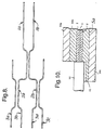
- a first layer (2) is supported on a substrate layer (1) which is held in position by a vacuum bed (4).
- the first layer (2) has retaining features (3) in the form of channels.
- a resin dispenser (5) provides a supply of resin (6) containing a photoinitiator to the line of contact formed between the first layer (2) and a second layer (7) supported on a substrate layer (8).
- the roller (9) applies a pressure along the line of contact and moves in the direction indicated by the arrow (A).
- the resin is thus squeezed across the surface of the first layer (2) by the action of the roller and into the retaining features (3) thereby only leaving a very small residual overlay of the resin between the second layer (7) which is superimposed over the first layer (2).
- UV light from the source (10) irradiates the resin and initiates the curing of the resin.
- Figure 2 is an optical device which has as a wave guide a so-called "Y" junction or splitter in which light is directed along the stem of the Y and is split between the two branches.
- Figure 3 shows a graphical representation of the intensity of the light signal as emitted from the branched end of the optical device as prepared in Example 1.
- the major peaks represent the light emitted from the actual branches of the "Y" junction.
- the absence of other peaks show that the optical device is able to retain substantially all of the light signal within the wave guide, i.e. There is little or no overlay present.
- Figure 4 is a similar graphical representation as that of Figure 3 except that the "Y" junction was that prepared in Example 2.
- the major peaks represent the light emitted from the actual branches of the "Y" junction.
- the presence of a substantial overlay allows leakage of the light signal from the wave guide which can be seen by the large number of minor peaks to either side of each major peak.
- Figure 5 shows a cross-section of the optical device as prepared in Example 1 comprising a first layer (2) having embossed, and filled, retaining features (3) and a second layer (7) As is evident there is little or no discernible overlay present.
- Figure 6 shows a cross-section of the optical device as prepared in Example 2 comprising a first layer (2) having embossed, and filled retaining features (3) and a second layer (7) Between the first layer (2) and second layer (7) there is an interposing, overlay (11).
- Figure 7 shows a graphical representation of the intensity of the light signal as emitted from the branched end of the optical device as prepared in Example 7.
- the major peaks represent the light emitted from the actual branches of the 1 x 8 passive splitter. The absence of other peaks shows that the optical device is able to retain substantially all of the light signal within the wave guide.
- Figure 8 is an optical component known as a 2 x 4 splitter.
- An incoming light signal from one or other of stems (1a, 1b) is progressively split into two signals along branches (2a, 2b) and thereafter four signals along branches (3a, 3b, 3c, 3d).
- Figure 9 shows a graphical representation of the intensity of the light signal as emitted from the ends of branches (3a, 3b, 3c, 3d) of the 2 x 4 splitter as shown in Figure 8 and fabricated according to the process of the present invention.
- the major peaks represent the light emitted from the ends of the branches.
- the absence of other peaks show that the optical device is able to retain substantially all of the light signal within the wave guide, i.e. there is little or no overlay present.
- the signal from each of the branches was within 0.1 dB of each other.
- Figure 10 shows how an optical fibre (12) may be abutted against a retaining feature (3) which has been filled with the second polymer.
- the retaining feature (3) is located within a first layer (2) over which has been applied further first polymer to form a second layer (7).
- the first layer (2) is supported by a substrate (5a) in which is formed a positioning feature (13) e.g. a "V" groove in which the optical fibre (12) is located.
- Further supporting layers (14a, 14b 14c) are also provided.
- This formulation was used to prepare the first polymer in which the at least one retaining feature was formed.
- the formulation contained
- the viscosity of the formulation was measured to be 0.4 Poise using a Carrimed rheometer.
- This formulation was used as the resin from which the retained second polymer was formed.
- the formulation contained
- Formulation B Using the method described for Formulation A, Formulation B provided an optical coating with a refractive index of 1.466.
- This formulation was based on Formulation B except that 5 parts by wt. of a viscosity modifying polymer of the general formula where R is ethyl acrylate was added.
- the formulation viscosity was 1.3 Poise.
- the viscosity of this formulation was similar to that of Formulation A and had a refractive index (when cured) of 1.4734 at 633 nm.
- a flexible substrate comprising polyethylene terephthalate film (Melinex grade 506 - Melinex is a tradename of Imperial Chemical Industries plc), 100 ⁇ m nominal thickness, was coated with Formulation A (50 ⁇ m wet coat thickness) using a No. 5 K bar coater and partially UV cured using a Fusion Systems UV lamp type LXF300, fitted with a type D bulb model No. 1787 emitting in the range 200-880 nm with maximum output at 365 nm, providing 118 W.cm-1 at the focal point.
- Polyethylene terephthalate film Melinex grade 506 - Melinex is a tradename of Imperial Chemical Industries plc
- Formulation A 50 ⁇ m wet coat thickness
- Retaining features, in the form of channels, were then embossed into the partially cured film which was then further cured at 20°C using the "Fusion Systems UV source to form a first layer.
- the retaining features were generally of a square cross-section (7.5 ⁇ m by 7.5 ⁇ m) in the form of a "Y" junction.
- the configuration of the "Y" junction is that shown in Figure 2 wherein the two arms join the stem of the Y as "S” bends of curve radius 150 mm.
- Each of the arms and stem were of 40 mm in length.
- the first layer was transferred to a table and held in position using a vacuum bed to form a supported film.
- the table was provided with a laminating roller (70 mm outside diameter including a 10 mm silicone rubber sleeve, width 64.5 mm) and a UV lamp (GEW serial No.8428, type MD2-10 fitted with a type 708A.FCD lamp providing the same output and wavelength range as the Fusion Systems lamp above). Both the laminating roller and the UV lamp were able to traverse the length of supported film.
- a line of contact was formed between a flexible dispensing layer of Melinex 400 film and the supported film.
- the UV lamp was positioned and the light therefrom focused (using a parabolic lens) such that illumination at a level of 120 W.cm-1 occurred along the line of contact.
- the laminating roller was positioned along the line of contact and a load of 68 kg applied to the roller.
- the laminating roller and the UV lamp traversed the length of the supported film at a rate of 0.5 m.s-1 such that an area of supported film of 65 mm by 65 mm was covered and during which time 0.2g of resin of Formulation B was dispensed using a pipette to the line of contact between the first and second film.
- the resin was thus squeezed across the surface of the supported film by the action of the roller thereby filling the retaining features and leaving only a small residual overlay of cured Formulation B between the laminated supported film and the dispensing film.
- the conditions of the experiment were therefore such that the time for cure of the resin in the retaining feature approximated to the residence time of the laminated films in the nip of the laminating roller.
- the dispensing layer was readily delaminated from the residual overlay.
- the overlay was then coated with a 50 ⁇ m thick layer of Formulation A which was then partially UV cured using the GEW UV source. Fabrication was then completed by laminating a substrate of Melinex 505 film onto the partially cured layer of Formulation A which was then fully UV cured to produce a laminated product.
- the laminated product was then baked in an oven at 80°C for 18 hours before testing.
- a sample of filled retaining feature was cut out of the baked laminated product and sectioned using a microtome.
- the thickness of the overlay in the microtomed sample was measured by optical microscopy to be 0.25 +/- 0.20 ⁇ m.
- the cross-sectional dimensions were also measured to be
- the effective refractive index difference between the cured Formulation B in the retaining feature and the surrounding region was determined to be 0.007.
- the "Y" shaped waveguides thus formed were prepared for optical characterisation by sandwiching them between two glass slides and microtoming the ends such that the end faces were perpendicular.
- Example 1 The procedure of Example 1 was repeated except the UV curing of the resin in the retaining feature was performed using a lower intensity UV source (Model B-100A Blak Ray Ultraviolet lamp, UVP Inc. with 1.0 mW.cm-2 at 38cm from the source) that was not directed along the line of contact. Therefore, in this example the reduced power of the UV light resulted in the curing time being less than the residence time at the nip with a consequential leakage of the resin from the retaining feature so as to form a thicker overlay.
- a lower intensity UV source Model B-100A Blak Ray Ultraviolet lamp, UVP Inc. with 1.0 mW.cm-2 at 38cm from the source
- the overlay thickness was measured subsequently determined and found to vary in the range 1.5 to 3.0 ⁇ m.
- Example 1 and Example 2 were characterised using fibre coupling techniques using "pigtailed" laser diodes having wavelengths of around 1.3 and 1.55 ⁇ m (Northern Telecom LC71-15 (1.32 ⁇ m) and LC81-18 (1.552 ⁇ m)).
- the output from the lasers was transmitted via a standard 9/125 ⁇ m silica monomode optical fibre, the end face of which was prepared using a standard fibre cleaving technique.
- a sandwiched waveguide of Example 1 was mounted on a 4-axis manipulator stage (Photon Control DM2), whilst the end of the optical fibre was mounted on an adjacent manipulator block (Photon Control Microblock). The end of the optical fibre was then brought into alignment with the input face of the "Y" shaped waveguide.
- the laser light was then coupled into the wave guide through a 2 to 10 mm wide air gap and was transmitted along the waveguide to the relevant output face.
- the light emitted from the output face was imaged using a microscope objective lens onto the sensing element of a vidicon camera (Electrophysics Micronviewer 7290).
- the lens was also mounted on a manipulator block in order to allow the appropriate section of the output face to be viewed.
- the image received by the vidicon was inputted into an image capture board (Synoptics Synapse 768) mounted in a Nectar 486 computer running an image analysis programme (PC Image Plus, Poster Findlay Associates).
- the programme allows the relative intensities of different sections of the received image to be measured and plotted.
- a straight waveguide prepared according to Example 1 showed a similar contrast ratio.
- Figure 4 shows the results of characterising the "Y" shaped waveguide prepared according to Example 2.
- the contrast ratio of about 7 is principally due to the thicker overlay.
- Straight waveguides produced according to Example 2 also showed a reduced contrast ratio of between 5 to 100.
- Example 1 was repeated except that Formulation C was used instead of Formulation B.
- the resulting laminated product had a similar thickness and variation in thickness to that of Example 1.
- Example 2 was repeated except that Formulation D was used instead of Formulation B.
- the filling of the retaining features was as described in Example 2.
- the resin in the retaining features was cured after the line of contact had passed over the filled portion of the retaining feature, thereby allowing the retained resin to partially relax out of the retaining feature, this resulted in the formation of a very large overlay.
- Example 1 was repeated except that Formulation E was used instead of Formulation B. An overlay comparable to that described in Example 1 was generated.
- Example 1 was repeated except that a multimode optical device was prepared comprising channels of 28 ⁇ m depth and of between 10 to 60 ⁇ m width.
- Formulation B was replaced by a resin comprising an epoxylated bis phenol A diacrylate having a refractive index of 1.5562 at 633 nm.
- Formulations E and F replaced Formulation B respectively.
- Example 6 In each of Example 6 (a), (b) and (c) an overlay comparable to that of Example 1 was produced.
- Example 1 was repeated except that a 1 x 8 passive splitter was formed and Formulation B was replaced by a resin comprising 90 parts by wt. of HFG and 10 parts by wt. of ethylene glycol dimethacrylate.
- An analysis comparable to that performed for Examples 1 and 2 was conducted and the results are as shown in Figure 7.
- the best total loss for the configuration was 16.6 +/- 1.6 dB with an average loss of 17.3 +/- 2.7 dB.
Abstract
Description
- The present invention relates to organic optical components and the preparation thereof.
- Optical components may be used to transmit and manipulate light signals in various fields of technology such as telecommunications, data communications, avionic control systems, sensor networks and automotive control systems.
- Generally such optical components are classed as either passive or active. Examples of passive optical components are those which provide the, polarisation control, transmission, distribution, splitting, combining, multiplexing and demultiplexing of the light signal. Active optical components include those requiring electrical connections to power and/or control circuitry, such as laser sources and photodiode detectors, and/or to manipulate the light signal using the electro-optic effect, such as provided by certain non-linear optical materials.
- It is known to use inorganic materials, such as silica on silicon and ion-exchanges glass, to produce passive optical components. The methods of manufacture of such inorganic passive optical components are based on the lithographic technologies used in the mass production of semiconductor wafers. However, the subsequent connecting of optical fibres to such components is complex and lengthy and requires the use of active alignment techniques which are increasingly more difficult as the complexity of the components increase.
- Inorganic active optical components can be prepared by the combination of active semiconductor materials, such as lithium niobate, into inorganic passive optical components, such as silica. However, the preparation of such active components is difficult such that their occurrence and use is uncommon.
- Organic passive optical components comprising polymeric materials are known using direct and indirect lithographic processes. In the indirect lithographic process a master pattern is formed from an organic or inorganic resist material. The master pattern is then replicated by electrodeposition to provide a series of moulds which are then filled with a suitable polymeric material to produce the organic passive optical components.
- Organic optical components usually comprise two or more polymers having different refractive indices. The polymer having the higher refractive index when surrounded by the other polymer can function as a wave guide which allows for the transmission and manipulation of a light signal. The higher refractive index polymer is usually introduced into the other polymer as a resin which is then cured. Such a resin needs to be introduced in a precise and controlled manner in order to reduce optical loss from the subsequent waveguide.
- DE-A-3 149 907 describes a polymeric structure for use in the preparation of an organic optical element and an organic optical component according to the preambles of Claims 1 and 8.
- Hitherto, the processes used in the preparation of such waveguides lead to the formation of a relatively thick and uneven residual layer of resin being present in the organic optical component which when cured results in a relatively thick layer of polymer of variable thickness which gives rise to problems such as unacceptably high optical losses, non-uniform output and inconsistent performance thereby reducing the incentive to use such organic optical components.
- It is an object of the present invention to provide an organic optical component having at least one significantly improved characteristic and a method which allows the mass production of such a component.
- Accordingly in a first aspect the present invention provides a polymeric structure for use in the preparation of an organic optical component which polymeric structure comprises
- (a) a first layer of an optically transmissive first polymer having a first refractive index, the first layer having a surface in which is defined at least one retaining feature;
- (b) an optically transmissive second polymer retained within the at least one retaining feature, the second polymer having a second refractive index which is greater than the first refractive index; and
- (c) an overlay of the second polymer having a maximum thickness of less than 1.5 µm over the surface of the first layer.
-
- In a second aspect of the present invention there is provided an organic optical component comprising
- (a) a first layer of an optically transmissive first polymer having a first refractive index, the first layer having a surface in which is defined at least one retaining feature;
- (b) an optically transmissive second polymer retained within the at least one retaining feature, the second polymer having a second refractive index which is greater than the first refractive index; and
- (c) a second layer of an optically transmissive third polymer having a third refractive
index which is less than the second refractive index and which is the same or different from
the first refractive index and which second layer contacts the second polymer retained within
the at least one retaining feature and the surface of the first layer
wherein the organic optical component exhibits an optical loss of less than 2.0 dB.cm-1 at at least one wavelength in the range 300 to 1600 nm and an overlay of the second polymer over the surface of the first layer has a maximum thickness of less than 1.5 µm. -
- In a third aspect of the present invention there is provided a method of preparing a polymeric structure having
- (i) a first layer of an optically transmissive first polymer having a first refractive index, the first layer having a surface in which is defined at least one retaining feature;
- (ii) an optically transmissive second polymer retained within the at least one retaining feature, the second polymer having a second refractive index which is greater than the first refractive index; and
- (iii) an overlay of the second polymer having a maximum thickness of less than 1.5 µm
over the surface of the first layer
which method comprises - (a) forming a line of contact between a flexible dispensing layer and the surface of the first layer and progressively contacting the surface with the flexible dispensing layer such that the line of contact advances across the surface;
- (b) applying sufficient of a resin, capable of being cured to form the second polymer and to substantially fill the at least one retaining feature, along the line of contact;
- (c) applying sufficient pressure along the line of contact such that
- (1) substantially all of the resin which is surplus to that required to fill the at least one retaining feature at the line of contact progresses with the advancing line of contact thereby filling the at least one retaining feature with resin; and
- (2) no more than a quantity of resin capable of forming the overlay of second polymer passes the line of contact; and
- (d) curing the resin filling the at least one retaining feature.
-
- The first layer may be supported by a suitable substrate which may be subsequently removed from the first layer. Alternatively, the substrate may remain with or is subsequently applied to the first layer thereby providing a laminate structure in which the relatively expensive first layer is of a thickness which is sufficient to provide the desired depth of retaining feature and complementary optical contrast and the substrate provides the desired level of support and may also provide additional positioning features for such items as optical fibres and other optical components. Thus in a preferred embodiment, the first layer is supported by a thicker support layer which possesses positioning grooves which are in alignment with the at least one retaining feature and which grooves are able to receive and locate optical fibres in abutment to the end of each at least one retaining feature. It is particularly preferred that the optical fibres are so located during the application of the second polymer and that sufficient of the second polymer is applied such that a suitable optically correct join is formed between the end of the retaining feature and the abutting end of the optical fibre.
- The second layer may also be supported by a suitable, optionally releasable, substrate. Conveniently, the dispensing layer provides the second layer such that the second layer is superimposed upon the surface as a consequence of the advancement of the line of contact. The second layer may also be provided with retaining features in which is retained an optically transmissive polymer, which may be the same as the second polymer and which may be so placed that at least some of the retaining features of the first layer are matched with at least some of the retaining features of the second layer such that they can form a composite optical component.
- The optically transmissive polymers may be selected from those known in the art including those developed as light curable adhesives for joining optical components for example those sold under the LUXTRAK (LUXTRAK is a tradename of ICI plc), those developed for polymer optical fibre fabrication and those developed for optical recording using polymer photoresists.
- In particular the optically transmissive second polymer may be formed from a suitable resin for example halogenated and deuterated siloxanes, acrylates and methacrylates such as ethyleneglycol dimethacrylate, tetrafluoropropylmethacrylate, pentafluorophenylmethacrylate, tetrachloroethylacrylate, multifunctional derivatives of triazine and phosphazene. Resins and polymers that contain highly fluorinated aliphatic and aromatic moieties, particularly those capable of being formed into cross-linked or covalent networks, are preferred. Additionally the second polymer may comprise a resin or polymer formulation that provides a non-linear optical (NLO) property such as described in European patent application EP-0474402-A, second order NLO properties, third order NLO properties or signal amplification properties.
- The optically transmissive first polymer in which the retaining feature is formed may be prepared from curable resins or can be fabricated from halogenated and deuterated polymers such as polymethylmethacrylate, polycarbonate, polystyrene and polyimides
- Suitably for the preparation of monomodal organic optical components, in particular those in which the retaining features have a height and a width from 5 to 10 µm, the difference between the second refractive index and the first refractive index is from 0.001 and 0.02, preferably from 0.002 and 0.01 and particularly from 0.004 and 0.007, i.e. the difference is from 0.05 to 1.5% of the first refractive index. Where the retaining features have a height and a width from 1 to 5 µm, and in which instance the reduction in the thickness of the overlay is even more advantageous, it is preferred that the difference in refractive index is from 1 to 30%, particularly 1 to 20%, and especially 1 to 5% of the first refractive index.
- Preferably, the second polymer has a refractive index from 1.4 and 1.7, for example from 1.43 and 1.5, and particularly from 1.45 and 1.46 at the wavelength of light used in the organic optical component. Where the optical component is multimodal it is preferred that the refractive index of the second polymer is from 1.5 to 1.7 and preferably about 1.6, for example 1.6 to 1.65.
- Where the second polymer is coupled to the end of an optical fibre it is preferred that the second polymer has a refractive index which closely matches that of the optical fibre. In such circumstances it is also preferred to select a second polymer which shows good intrinsic adhesion to the optical fibre which is principally formed from silica.
- The refractive index of the polymers may be modified by the inclusion of suitable additives into the polymer, in particular mixtures of those polymers mentioned above may be used to achieve a desired refractive index. Where the major component of the second polymer is bis(oxy ethyl methacrylate) 2,2',3,3',4,4' hexafluoroglutarate, it is particularly preferred that the refractive index of the second polymer is adjusted by adding appropriate amounts of ethylene glycol dimethacrylate which can increase the refractive index (as measured at 1.32 or 1.55 µm) by an absolute value in excess of 0.02 when added at a level of 30% by weight.
- The overlay of the second polymer has a maximum thickness of less than 1.5 µm, preferably less than 1 µm, and particularly less than 0.5 µm over the surface of the first layer. The average thickness of the overlay is preferably less than 1 µm and particularly less than 0.5 µm. The variation of the thickness of the overlay across the surface is preferably less than ± 0.75 µm, particularly less than ± 0.5 µm and especially less than ± 0.25 µm. When formed into an organic optical component the component will exhibit an optical loss of less than 2.0 dB.cm-1, preferably less than 1.0 dB.cm-1 and particularly less than 0.5 dB.cm-1.
- The at least one retaining feature is conveniently in the form of a channel, and typically is of a generally trapezoidal cross-section although other configurations are possible, for example rectangular, square or semi-circular. As stated above, for a monomodal organic optical device, the height and width of a retaining feature may be in the range 1 to 10 µm depending on the difference in refractive index used. However, preferably the height and width of the retaining features are in the range 5 to 10 µm, and particularly in the range 6 to 8µm. Preferably the maximum width of the retaining feature is at the surface of the first layer. Typically, the ratio of the maximum width to minimum width is less than 2:1 and is preferably about 1:1. The retaining feature may be formed by any suitable technique for example a lithographic etching process such as reactive ion etching through a suitable mask although moulding or embossing is preferred. Where the organic optical device is to be used as a multimodal device then similar fabrication techniques can be used with suitable adaptation of the dimensions and selection of materials, usually though the height and width of the retaining features when employed in a multimodal device are in the
range 10 to 100 µm, for example 10 to 50 µm and consequently the presence of an overlay is less of a problem than in the case of a monomodal device. - In order to facilitate the curing of the resin it is preferred to use an initiator, for example a thermal and/or photoinitiator and particularly an initiator which does not absorb light at the operating wave length of the organic optical component. Typically, when used, an initiator is present in the resin at a concentration from 0.1 to 3.0 % by weight, and preferably from 0.5 to 2.0 % by weight. Suitable photoinitiators include 2-methyl-1-[4-(methylthio)phenyl)-2-morpholino propanone-1 (Irgacure 907), 1-hydroxy-cyclohexyl-phenyl ketone (Irgacure 184), isopropylthioxanthone (Quantacure ITX),Camphorquinone/dimethylaminoethylmethacrylate. Similarly a suitable thermal initiator is tert-butylperoxy-2-ethyl hexanoate (Interox TBPEH).
- As the line of contact moves across the surface of the first layer the resin is effectively pushed across the surface and flows into the at least one retaining feature. The rate at which the line of contact advances across the surface will depend, amongst other things, on the characteristics of the resin. Typically, the resin has a viscosity from 0.1 to 100 poise and more typically from 10 to 100 poise. Preferably the line of contact is moved along the length of the retaining feature, particularly when the retaining feature has a width or height greater than 10 µm, thereby improving the filling of the retaining feature and reducing the possibility of inclusion of gas bubbles.
- The resin may be fully retained within a retaining feature as the line of contact moves from the retaining feature, in which case the resin may be cured at any convenient subsequent time. However, the resin may often show some degree of resilience in the non-cured form in which case as the line of contact moves from the retaining feature the resin therein will tend to relax and stand proud of the retaining feature thereby reducing the effectiveness of any optical component subsequently formed from the polymeric structure. To counter the relaxation of the resin it is preferred that the resin is cured whilst the line of contact passes over it. Conveniently and preferably therefore, the resin contains a photoinitiator which is activated by a particular wavelength of light, particularly UV light. A suitable source of light may then used to cure the resin before the pressure applied along the line of contact is released and before the resin relaxes from the retaining feature. It is especially preferred that the dispensing layer is transparent to the light used and that the light is shone through the dispensing layer towards the resin. In order to focus the light substantially at the tip and thereby avoiding, for example, premature curing of the resin, the angle of incidence of the light onto the line of contact may be required to be adjusted from polymer to polymer. Alternatively, for a given angle of incidence and where the first layer is at least partially transmissive to the light, the first layer may be chosen to have a thickness such that the internal refraction of the incident light acts to focus the light at the line of contact. Additionally, where the first layer is at least partially transmissive to the light and is of a suitable thickness, a mirrored support may be positioned under the first layer thereby causing the transmitted light to be reflected back to the line of contact.
- The pressure is applied along the line of contact by any suitable means. Suitably, the pressure is applied using a roller under a compressive load which may thus on rotation retain the resin in the nip formed by the roller between the buffer layer and the surface. It is therefore preferred that the resin is cured at the nip as the line of contact progresses across the surface.
- The present invention is illustrated by reference to the following figures.
- Figure 1 shows a schematic diagram of an organic optical component being formed according to the process of the present invention.
- Figure 2 shows an optical device capable of being formed by the process of the present invention.
- Figure 3 shows an analysis of the output of the optical device formed in Example 1.
- Figure 4 shows an analysis of the output of the optical device formed in Example 2.
- Figure 5 is a cross-section of the branched end of the device formed in Example 1.
- Figure 6 is a cross-section of the stem end of the device formed in Example 2.
- Figure 7 shows an analysis of the output of the optical device formed in Example 7.
- Figure 8 shows an additional optical device capable of being formed by the process of the present invention.
- Figure 9 shows an analysis of the output of the optical device as shown in Figure 8.
- Figure 10 shows the positioning of an optical fibre within an optical device capable of being formed by the process of the present invention
-
- In Figure 1, a first layer (2) is supported on a substrate layer (1) which is held in position by a vacuum bed (4). The first layer (2) has retaining features (3) in the form of channels. A resin dispenser (5) provides a supply of resin (6) containing a photoinitiator to the line of contact formed between the first layer (2) and a second layer (7) supported on a substrate layer (8). The roller (9) applies a pressure along the line of contact and moves in the direction indicated by the arrow (A). The resin is thus squeezed across the surface of the first layer (2) by the action of the roller and into the retaining features (3) thereby only leaving a very small residual overlay of the resin between the second layer (7) which is superimposed over the first layer (2). As the resin filled retaining features pass through the nip of the roller, UV light from the source (10) irradiates the resin and initiates the curing of the resin.
- Figure 2 is an optical device which has as a wave guide a so-called "Y" junction or splitter in which light is directed along the stem of the Y and is split between the two branches.
- Figure 3 shows a graphical representation of the intensity of the light signal as emitted from the branched end of the optical device as prepared in Example 1. The major peaks represent the light emitted from the actual branches of the "Y" junction. The absence of other peaks show that the optical device is able to retain substantially all of the light signal within the wave guide, i.e. There is little or no overlay present.
- Figure 4 is a similar graphical representation as that of Figure 3 except that the "Y" junction was that prepared in Example 2. As before, the major peaks represent the light emitted from the actual branches of the "Y" junction. However, The presence of a substantial overlay allows leakage of the light signal from the wave guide which can be seen by the large number of minor peaks to either side of each major peak.
- Figure 5 shows a cross-section of the optical device as prepared in Example 1 comprising a first layer (2) having embossed, and filled, retaining features (3) and a second layer (7) As is evident there is little or no discernible overlay present.
- Figure 6 shows a cross-section of the optical device as prepared in Example 2 comprising a first layer (2) having embossed, and filled retaining features (3) and a second layer (7) Between the first layer (2) and second layer (7) there is an interposing, overlay (11).
- Figure 7 shows a graphical representation of the intensity of the light signal as emitted from the branched end of the optical device as prepared in Example 7. The major peaks represent the light emitted from the actual branches of the 1 x 8 passive splitter. The absence of other peaks shows that the optical device is able to retain substantially all of the light signal within the wave guide.
- Figure 8 is an optical component known as a 2 x 4 splitter. An incoming light signal from one or other of stems (1a, 1b) is progressively split into two signals along branches (2a, 2b) and thereafter four signals along branches (3a, 3b, 3c, 3d).
- Figure 9 shows a graphical representation of the intensity of the light signal as emitted from the ends of branches (3a, 3b, 3c, 3d) of the 2 x 4 splitter as shown in Figure 8 and fabricated according to the process of the present invention. The major peaks represent the light emitted from the ends of the branches. The absence of other peaks show that the optical device is able to retain substantially all of the light signal within the wave guide, i.e. there is little or no overlay present. The signal from each of the branches was within 0.1 dB of each other.
- Figure 10 shows how an optical fibre (12) may be abutted against a retaining feature (3) which has been filled with the second polymer. The retaining feature (3) is located within a first layer (2) over which has been applied further first polymer to form a second layer (7). the first layer (2) is supported by a substrate (5a) in which is formed a positioning feature (13) e.g. a "V" groove in which the optical fibre (12) is located. Further supporting layers (14a,
14b 14c) are also provided. - The invention is also illustrated by the following examples.
- This formulation was used to prepare the first polymer in which the at least one retaining feature was formed. The formulation contained
- 100 parts by wt. of bis(oxy ethyl methacrylate) 2,2',3,3',4,4' hexafluoroglutarate (HFG)
- 2 parts by wt. of "Irgacure 651" (Ciba-Geigy)
- 1 part by wt. tert-butylperoxy-2-ethyl hexanoate ("Interox TBPEH", Interox Chemicals Ltd).
-
- The viscosity of the formulation was measured to be 0.4 Poise using a Carrimed rheometer.
- When spin coated to a thickness of 10µm onto a high refractive index substrate a fully cured optical coating of Formulation A had a refractive index of 1.449 obtained using the critical angle method.
- This formulation was used as the resin from which the retained second polymer was formed. The formulation contained
- 75 parts by wt. of HFG
- 25 parts by wt. of 1,3,5 tris(oxy ethyl methacrylate) triazine
- 2 parts by wt. of "Irgacure 651"
- 1 part by wt. of "Interox TBPEH". The formulation viscosity was 0.8 Poise.
-
- Using the method described for Formulation A, Formulation B provided an optical coating with a refractive index of 1.466.
- This formulation was used as an alternative to Formulation B. The formulation contained
- 92.5 parts by wt. of HFG
- 7.5 parts by wt. of ethylene glycol dimethacrylate
- 2 parts by wt. of "Irgacure 651"
- 1 part by wt. of "Interox TBPEH" The formulation viscosity was the same as that of Formulation A. The refractive index was 1.4623 at 1.32 µm and 1.4605 at 1.55 µm.
-
- This formulation was based on Formulation B except that 5 parts by wt. of a viscosity modifying polymer of the general formulawhere R is ethyl acrylate

was added. - The formulation viscosity was 1.3 Poise.
- This formulation contained
- 100 parts by wt. of an aliphatic polyester acrylate ("Photomer 5018", Harcros Chemicals)
- 2 parts by wt. of "Irgacure 651"
- 1 part by wt. of "Interox TBPEH". The formulation had a viscosity at 25°C of between 7 to 12 Poise and a refractive index (when cured) of 1.488 at 633 nm (Formulation A which had a refractive index of 1.4638 at 633 nm).
-
- This formulation contained
- 75 parts by wt. of HFG
- 25 parts by wt. of ethylene glycol dimethacrylate
- 2 parts by wt. of "Irgacure 651"
- 1 part by wt. of "Interox TBPEH".
-
- The viscosity of this formulation was similar to that of Formulation A and had a refractive index (when cured) of 1.4734 at 633 nm.
- A flexible substrate comprising polyethylene terephthalate film (Melinex grade 506 - Melinex is a tradename of Imperial Chemical Industries plc), 100 µm nominal thickness, was coated with Formulation A (50 µm wet coat thickness) using a No. 5 K bar coater and partially UV cured using a Fusion Systems UV lamp type LXF300, fitted with a type D bulb model No. 1787 emitting in the range 200-880 nm with maximum output at 365 nm, providing 118 W.cm-1 at the focal point.
- Retaining features, in the form of channels, were then embossed into the partially cured film which was then further cured at 20°C using the "Fusion Systems UV source to form a first layer.
- The retaining features were generally of a square cross-section (7.5 µm by 7.5 µm) in the form of a "Y" junction. The configuration of the "Y" junction is that shown in Figure 2 wherein the two arms join the stem of the Y as "S" bends of curve radius 150 mm. Each of the arms and stem were of 40 mm in length.
- The first layer was transferred to a table and held in position using a vacuum bed to form a supported film. The table was provided with a laminating roller (70 mm outside diameter including a 10 mm silicone rubber sleeve, width 64.5 mm) and a UV lamp (GEW serial No.8428, type MD2-10 fitted with a type 708A.FCD lamp providing the same output and wavelength range as the Fusion Systems lamp above). Both the laminating roller and the UV lamp were able to traverse the length of supported film.
- A line of contact was formed between a flexible dispensing layer of Melinex 400 film and the supported film. The UV lamp was positioned and the light therefrom focused (using a parabolic lens) such that illumination at a level of 120 W.cm-1 occurred along the line of contact. The laminating roller was positioned along the line of contact and a load of 68 kg applied to the roller.
- The laminating roller and the UV lamp traversed the length of the supported film at a rate of 0.5 m.s-1 such that an area of supported film of 65 mm by 65 mm was covered and during which time 0.2g of resin of Formulation B was dispensed using a pipette to the line of contact between the first and second film.
- The resin was thus squeezed across the surface of the supported film by the action of the roller thereby filling the retaining features and leaving only a small residual overlay of cured Formulation B between the laminated supported film and the dispensing film. The conditions of the experiment were therefore such that the time for cure of the resin in the retaining feature approximated to the residence time of the laminated films in the nip of the laminating roller.
- The dispensing layer was readily delaminated from the residual overlay. The overlay was then coated with a 50 µm thick layer of Formulation A which was then partially UV cured using the GEW UV source. Fabrication was then completed by laminating a substrate of Melinex 505 film onto the partially cured layer of Formulation A which was then fully UV cured to produce a laminated product. The laminated product was then baked in an oven at 80°C for 18 hours before testing.
- A sample of filled retaining feature was cut out of the baked laminated product and sectioned using a microtome. The thickness of the overlay in the microtomed sample was measured by optical microscopy to be 0.25 +/- 0.20 µm. The cross-sectional dimensions were also measured to be
- depth 7.5 µm
- width at surface of first layer 7.4 µm
- width at bottom of channel 7.1 µm.
-
- The effective refractive index difference between the cured Formulation B in the retaining feature and the surrounding region was determined to be 0.007.
- The "Y" shaped waveguides thus formed were prepared for optical characterisation by sandwiching them between two glass slides and microtoming the ends such that the end faces were perpendicular.
- The procedure of Example 1 was repeated except the UV curing of the resin in the retaining feature was performed using a lower intensity UV source (Model B-100A Blak Ray Ultraviolet lamp, UVP Inc. with 1.0 mW.cm-2 at 38cm from the source) that was not directed along the line of contact. Therefore, in this example the reduced power of the UV light resulted in the curing time being less than the residence time at the nip with a consequential leakage of the resin from the retaining feature so as to form a thicker overlay.
- The overlay thickness was measured subsequently determined and found to vary in the range 1.5 to 3.0 µm.
- The wave guides formed in Example 1 and Example 2 were characterised using fibre coupling techniques using "pigtailed" laser diodes having wavelengths of around 1.3 and 1.55 µm (Northern Telecom LC71-15 (1.32 µm) and LC81-18 (1.552 µm)).
- The output from the lasers was transmitted via a
standard 9/125 µm silica monomode optical fibre, the end face of which was prepared using a standard fibre cleaving technique. - A sandwiched waveguide of Example 1 was mounted on a 4-axis manipulator stage (Photon Control DM2), whilst the end of the optical fibre was mounted on an adjacent manipulator block (Photon Control Microblock). The end of the optical fibre was then brought into alignment with the input face of the "Y" shaped waveguide.
- The laser light was then coupled into the wave guide through a 2 to 10 mm wide air gap and was transmitted along the waveguide to the relevant output face. The light emitted from the output face was imaged using a microscope objective lens onto the sensing element of a vidicon camera (Electrophysics Micronviewer 7290). The lens was also mounted on a manipulator block in order to allow the appropriate section of the output face to be viewed.
- The image received by the vidicon was inputted into an image capture board (Synoptics Synapse 768) mounted in a Nectar 486 computer running an image analysis programme (PC Image Plus, Poster Findlay Associates). The programme allows the relative intensities of different sections of the received image to be measured and plotted.
- The output from the two arms of the "Y" shaped wave guide is shown in Figure 3. The confinement of the light centred on the regions of the retaining features is clear. No significant light intensity is seen in the region between the two output peaks and the contrast ratio (as determined by the maximum intensity of the peaks divided by the maximum intensity between the peaks is in excess of 1000). Thus, little light is emitted from the overlay of the cured Formulation B resin.
- In a further example, a straight waveguide prepared according to Example 1 showed a similar contrast ratio.
- In comparison, Figure 4 shows the results of characterising the "Y" shaped waveguide prepared according to Example 2. The contrast ratio of about 7 is principally due to the thicker overlay. Straight waveguides produced according to Example 2 also showed a reduced contrast ratio of between 5 to 100.
- Example 1 was repeated except that Formulation C was used instead of Formulation B. The resulting laminated product had a similar thickness and variation in thickness to that of Example 1.
- Example 2 was repeated except that Formulation D was used instead of Formulation B. The filling of the retaining features was as described in Example 2. The resin in the retaining features was cured after the line of contact had passed over the filled portion of the retaining feature, thereby allowing the retained resin to partially relax out of the retaining feature, this resulted in the formation of a very large overlay.
- Example 1 was repeated except that Formulation E was used instead of Formulation B. An overlay comparable to that described in Example 1 was generated.
- Example 1 was repeated except that a multimode optical device was prepared comprising channels of 28 µm depth and of between 10 to 60 µm width. In Example 6 (a), Formulation B was replaced by a resin comprising an epoxylated bis phenol A diacrylate having a refractive index of 1.5562 at 633 nm. In examples 6 (b) and 6 (c) Formulations E and F replaced Formulation B respectively.
- In each of Example 6 (a), (b) and (c) an overlay comparable to that of Example 1 was produced.
- Example 1 was repeated except that a 1 x 8 passive splitter was formed and Formulation B was replaced by a resin comprising 90 parts by wt. of HFG and 10 parts by wt. of ethylene glycol dimethacrylate. An analysis comparable to that performed for Examples 1 and 2 was conducted and the results are as shown in Figure 7. The best total loss for the configuration was 16.6 +/- 1.6 dB with an average loss of 17.3 +/- 2.7 dB.
Claims (17)
- A polymeric structure for use in the preparation of an organic optical component which polymeric structure comprises(a) a first layer (2) of an optically transmissive first polymer having a first refractive index, the first layer having a surface in which is defined at least one retaining feature (3);(b) an optically transmissive second polymer retained within the at least one retaining feature (3), the second polymer having a second refractive index which is greater than the first refractive index; characterised by(c) an overlay (11) of the second polymer having a maximum thickness of less than 1.5 µm over the surface of the first layer.
- A polymeric structure as claimed in Claim 1 wherein the first layer (2) is supported by a substrate which is removable from the first layer.
- A polymeric structure as claimed in either Claim 1 or Claim 2 wherein the first and second polymers are selected from light curable adhesives for joining optical components, polymers for optical fibre fabrication and polymer photoresists for optical recording.
- A polymeric structure as claimed in any of Claims 1 to 3 wherein the second polymer is formed from a resin derived from monomers selected from at least one of halogenated and deuterated siloxanes, acrylates and methacrylates and multifunctional derivatives of triazine and phosphazene.
- A polymeric structure as claimed in Claim 3 wherein the second polymer is formed from a resin derived from monomers selected from at least one of ethyleneglycol dimethacrylate, tetrafluoropropyl methacrylate, pentafluorophenyl methacrylate, tetrachloroethylacrylate, bis (oxyethyl methacrylate) hexafluoroglutarate, ethyleneglycol dimethacrylate and tris (oxyethyl methacrylate) triazine.
- A polymeric structure as claimed in any of Claims 1 to 4 wherein the refractive index of the first and second polymer is modified by inclusion of an additive, or by using mixtures of resins to achieve a desired refractive index.
- A polymeric structure as claimed in any of Claims 1 to 5 for use in a multimodal optical component wherein the at least one retaining feature (3) has height and width in the range 10 to 100 µm.
- A polymeric structure as claimed in Claim 7 wherein the at least one retaining feature (3) has height and width in the range 10 to 50 µm.
- A polymeric structure as claimed in any one of Claims 1 to 5 wherein the at least one retaining feature (3) has height and width in the range 1 to 10 µm.
- A polymeric structure as claimed in any one of Claims 1 to 5 wherein the at least one retaining feature (3) has height and width in the range 5 to 10 µm.
- A polymeric structure as claimed in any one of Claims 1 to 5 wherein the at least one retaining feature (3) has height and width in the range 1 to 5 µm.
- A polymeric structure as claimed in any one of Claims 1 to 11 wherein the variation of the thickness of the overlay (11) across the surface is less than ± 0.75 µm.
- An organic optical component comprising(a) a first layer (2) of an optically transmissive first polymer having a first refractive index, the first layer having a surface in which is defined at least one retaining feature;(b) an optically transmissive second polymer retained within the at least one retaining feature (3), the second polymer having a second refractive index which is greater than the first refractive index; and(c) a second layer (7) of an optically transmissive third polymer having a third refractive index which is less than the second refractive index and which is the same or different from the first refractive index and which second layer (7) contacts the second polymer retained within the at least one retaining feature and the surface of the first layer,
characterised in that the organic optical component exhibits an optical loss of less than 2.0 dB.cm-1 at at least one wavelength in the range 300 to 1600 nm and in that an overlay of the second polymer over the surface of the first layer has a maximum thickness of less than 1.5 µm. - A method capable of preparing a polymeric structure as claimed in any one of Claims 1 to 12, which polymeric structure has(i) a first layer (2) of an optically transmissive first polymer having a first refractive index, the first layer having a surface in which is defined at least one retaining feature;(ii) an optically transmissive second polymer retained within the at least one retaining feature, the second polymer having a second refractive index which is greater than the first refractive index; and(iii) an overlay (11) of the second polymer having a maximum thickness of less than 1.5 µm over the surface of the first layer (2) which method comprises(a) forming a line of contact between a flexible dispensing layer and the surface of the first layer (2) and progressively contacting the surface with the flexible dispensing layer such that the line of contact advances across the surface;(b) applying sufficient of a resin, capable of being cured to form the second polymer and to substantially fill the at least one retaining feature, along the line of contact;(c) applying sufficient pressure along the line of contact such that(1) substantially all of the resin which is surplus to that required to fill the at least one retaining feature at the line of contact progresses with the advancing line of contact thereby filling the at least one retaining feature with resin; and(2) no more than a quantity of resin capable of forming the overlay (11) of second polymer passes the line of contact; and(d) curing the resin filling the at least one retaining feature.
- A method as claimed in Claim 14 wherein the resin is cured as it passes the line of contact.
- A method as claimed in Claim 15 wherein the resin is capable of being cured by means of a suitable source of light, wherein the dispensing layer is transparent to the light used and the light is shone through the dispensing layer towards the resin at a given angle of incidence of the light onto the line of contact.
- A polymeric structure as claimed in any of Claims 1 to 12, said polymeric structure being an optical waveguide.
Applications Claiming Priority (3)
| Application Number | Priority Date | Filing Date | Title |
|---|---|---|---|
| GB939320326A GB9320326D0 (en) | 1993-10-01 | 1993-10-01 | Organic optical components and preparation thereof |
| GB9320326 | 1993-10-01 | ||
| PCT/GB1994/002118 WO1995009726A1 (en) | 1993-10-01 | 1994-09-29 | Organic optical components and preparation thereof |
Publications (2)
| Publication Number | Publication Date |
|---|---|
| EP0722387A1 EP0722387A1 (en) | 1996-07-24 |
| EP0722387B1 true EP0722387B1 (en) | 2000-09-06 |
Family
ID=10742888
Family Applications (1)
| Application Number | Title | Priority Date | Filing Date |
|---|---|---|---|
| EP94927745A Expired - Lifetime EP0722387B1 (en) | 1993-10-01 | 1994-09-29 | Organic optical components and preparation thereof |
Country Status (9)
| Country | Link |
|---|---|
| US (2) | US5985084A (en) |
| EP (1) | EP0722387B1 (en) |
| AT (1) | ATE196111T1 (en) |
| AU (1) | AU7704594A (en) |
| DE (1) | DE69425831T2 (en) |
| ES (1) | ES2151932T3 (en) |
| GB (2) | GB9320326D0 (en) |
| TW (1) | TW267216B (en) |
| WO (1) | WO1995009726A1 (en) |
Families Citing this family (69)
| Publication number | Priority date | Publication date | Assignee | Title |
|---|---|---|---|---|
| FR876M (en) | 1960-10-12 | 1961-10-16 | ||
| AUPN718195A0 (en) | 1995-12-18 | 1996-01-18 | Sola International Holdings Ltd | Laminate wafers |
| GB9623185D0 (en) | 1996-11-09 | 1997-01-08 | Epigem Limited | Improved micro relief element and preparation thereof |
| US6473220B1 (en) * | 1998-01-22 | 2002-10-29 | Trivium Technologies, Inc. | Film having transmissive and reflective properties |
| US6272275B1 (en) | 1999-06-25 | 2001-08-07 | Corning Incorporated | Print-molding for process for planar waveguides |
| US6933098B2 (en) | 2000-01-11 | 2005-08-23 | Sipix Imaging Inc. | Process for roll-to-roll manufacture of a display by synchronized photolithographic exposure on a substrate web |
| US6930818B1 (en) * | 2000-03-03 | 2005-08-16 | Sipix Imaging, Inc. | Electrophoretic display and novel process for its manufacture |
| US6672921B1 (en) | 2000-03-03 | 2004-01-06 | Sipix Imaging, Inc. | Manufacturing process for electrophoretic display |
| US6833943B2 (en) | 2000-03-03 | 2004-12-21 | Sipix Imaging, Inc. | Electrophoretic display and novel process for its manufacture |
| US7158282B2 (en) | 2000-03-03 | 2007-01-02 | Sipix Imaging, Inc. | Electrophoretic display and novel process for its manufacture |
| US7557981B2 (en) | 2000-03-03 | 2009-07-07 | Sipix Imaging, Inc. | Electrophoretic display and process for its manufacture |
| US6885495B2 (en) * | 2000-03-03 | 2005-04-26 | Sipix Imaging Inc. | Electrophoretic display with in-plane switching |
| US6947202B2 (en) * | 2000-03-03 | 2005-09-20 | Sipix Imaging, Inc. | Electrophoretic display with sub relief structure for high contrast ratio and improved shear and/or compression resistance |
| US20070237962A1 (en) | 2000-03-03 | 2007-10-11 | Rong-Chang Liang | Semi-finished display panels |
| US6788449B2 (en) * | 2000-03-03 | 2004-09-07 | Sipix Imaging, Inc. | Electrophoretic display and novel process for its manufacture |
| US7715088B2 (en) | 2000-03-03 | 2010-05-11 | Sipix Imaging, Inc. | Electrophoretic display |
| US7052571B2 (en) | 2000-03-03 | 2006-05-30 | Sipix Imaging, Inc. | Electrophoretic display and process for its manufacture |
| US6831770B2 (en) | 2000-03-03 | 2004-12-14 | Sipix Imaging, Inc. | Electrophoretic display and novel process for its manufacture |
| US6829078B2 (en) | 2000-03-03 | 2004-12-07 | Sipix Imaging Inc. | Electrophoretic display and novel process for its manufacture |
| US7233429B2 (en) | 2000-03-03 | 2007-06-19 | Sipix Imaging, Inc. | Electrophoretic display |
| US6865012B2 (en) | 2000-03-03 | 2005-03-08 | Sipix Imaging, Inc. | Electrophoretic display and novel process for its manufacture |
| US7408696B2 (en) | 2000-03-03 | 2008-08-05 | Sipix Imaging, Inc. | Three-dimensional electrophoretic displays |
| AU2001296902A1 (en) * | 2000-10-20 | 2002-05-06 | Corning Incorporated | Using deuterated source gases to fabricate low loss germanium-doped silicon oxy nitride (gestion-sion) |
| JP2002205312A (en) * | 2000-11-10 | 2002-07-23 | Dainippon Printing Co Ltd | Method and apparatus for producing lens sheet |
| JP2004514941A (en) * | 2000-11-28 | 2004-05-20 | フォトン−エックス インコーポレイテッド | Thin-film optical waveguide |
| JP2002160230A (en) * | 2000-11-28 | 2002-06-04 | Dainippon Printing Co Ltd | Method and apparatus for producing lens sheet |
| US8282762B2 (en) * | 2001-01-11 | 2012-10-09 | Sipix Imaging, Inc. | Transmissive or reflective liquid crystal display and process for its manufacture |
| US6795138B2 (en) | 2001-01-11 | 2004-09-21 | Sipix Imaging, Inc. | Transmissive or reflective liquid crystal display and novel process for its manufacture |
| WO2002072352A1 (en) * | 2001-03-12 | 2002-09-19 | Solidimension Ltd. | Method and apparatus for adhering sheets together without trapped bubbles and easy detachment of stack |
| US6677868B2 (en) * | 2001-03-16 | 2004-01-13 | Sharp Laboratories Of America, Inc. | Entropy coding with adaptive syntax to replace high probability symbols with lower probabilities symbols |
| AU2002307120A1 (en) * | 2001-05-07 | 2002-11-18 | Corning Incorporated | Photosensitive material suitable for making waveguides and method of making waveguides utilizing this photosensitive optical material |
| US6599957B2 (en) | 2001-05-07 | 2003-07-29 | Corning Incorporated | Photosensitive material suitable for making waveguides and method of making waveguides utilizing this photosensitive optical material |
| TW527529B (en) * | 2001-07-27 | 2003-04-11 | Sipix Imaging Inc | An improved electrophoretic display with color filters |
| TW539928B (en) | 2001-08-20 | 2003-07-01 | Sipix Imaging Inc | An improved transflective electrophoretic display |
| TWI308231B (en) * | 2001-08-28 | 2009-04-01 | Sipix Imaging Inc | Electrophoretic display |
| JP3846284B2 (en) * | 2001-11-26 | 2006-11-15 | 株式会社トッパンNecサーキットソリューションズ | Manufacturing method of optical waveguide |
| US6618537B2 (en) * | 2002-01-14 | 2003-09-09 | Applied Wdm, Inc. | Optical waveguide structures and methods of fabrication |
| US7595934B2 (en) | 2002-03-26 | 2009-09-29 | Brilliant Film Llc | Integrated sub-assembly having a light collimating or transflecting device |
| US7345824B2 (en) | 2002-03-26 | 2008-03-18 | Trivium Technologies, Inc. | Light collimating device |
| US6826345B1 (en) | 2002-06-10 | 2004-11-30 | Lightwave Microsystems Corporation | Top cap process for reducing polarization dependent wavelength shift in planar lightwave circuits |
| AU2003254775A1 (en) * | 2002-07-30 | 2004-02-16 | Toagosei Co., Ltd. | Composition for holography, method of curing the same, and cured article |
| TWI297089B (en) * | 2002-11-25 | 2008-05-21 | Sipix Imaging Inc | A composition for the preparation of microcups used in a liquid crystal display, a liquid crystal display comprising two or more layers of microcup array and process for its manufacture |
| US8023071B2 (en) * | 2002-11-25 | 2011-09-20 | Sipix Imaging, Inc. | Transmissive or reflective liquid crystal display |
| US7070406B2 (en) * | 2003-04-29 | 2006-07-04 | Hewlett-Packard Development Company, L.P. | Apparatus for embossing a flexible substrate with a pattern carried by an optically transparent compliant media |
| US6808646B1 (en) | 2003-04-29 | 2004-10-26 | Hewlett-Packard Development Company, L.P. | Method of replicating a high resolution three-dimensional imprint pattern on a compliant media of arbitrary size |
| US7573550B2 (en) * | 2003-05-20 | 2009-08-11 | Brilliant Film, Llc | Devices for use in non-emissive displays |
| US6967118B2 (en) * | 2004-03-09 | 2005-11-22 | Hewlett-Packard Development Company, L.P. | Process for creating Metal-Insulator-Metal devices |
| US7716823B2 (en) * | 2004-04-08 | 2010-05-18 | Hewlett-Packard Development Company, L.P. | Bonding an interconnect to a circuit device and related devices |
| JP2006154447A (en) * | 2004-11-30 | 2006-06-15 | Nitto Denko Corp | Manufacturing method of film-like optical waveguide |
| BRPI0607463A2 (en) * | 2005-02-15 | 2009-09-08 | Rpo Pty Ltd | photolithographic standardization of polymeric materials |
| US7908905B2 (en) * | 2005-08-31 | 2011-03-22 | The University Of Akron | Rheometer allowing direct visualization of continuous simple shear in non-newtonian fluid |
| US7799885B2 (en) | 2005-11-30 | 2010-09-21 | Corning Incorporated | Photo or electron beam curable compositions |
| US8529993B2 (en) * | 2006-05-01 | 2013-09-10 | Zetta Research andDevelopment LLC—RPO Series | Low volatility polymers for two-stage deposition processes |
| US7811640B2 (en) * | 2006-05-02 | 2010-10-12 | Rpo Pty Limited | Methods for fabricating polymer optical waveguides on large area panels |
| US8287895B1 (en) * | 2008-04-24 | 2012-10-16 | Hrl Laboratories, Llc | Three-dimensional biological scaffold compromising polymer waveguides |
| US8197930B1 (en) | 2007-05-10 | 2012-06-12 | Hrl Laboratories, Llc | Three-dimensional ordered open-cellular structures |
| US8226253B2 (en) | 2008-02-27 | 2012-07-24 | Lubart Neil D | Concentrators for solar power generating systems |
| US8173045B2 (en) | 2008-05-28 | 2012-05-08 | University Of Washington | Diels-Alder crosslinkable dendritic nonlinear optic chromophores and polymer composites |
| GB201007669D0 (en) | 2010-05-07 | 2010-06-23 | Epigem Ltd | Composite electrode for molecular electronic devices and method of manufacture thereof |
| US8798432B2 (en) * | 2010-10-21 | 2014-08-05 | Microsoft Corporation | Fabrication of a laminated optical wedge |
| US8765357B2 (en) * | 2011-04-19 | 2014-07-01 | Sumitomo Chemical Company, Limited | Resin and photoresist composition comprising same |
| US9539773B2 (en) | 2011-12-06 | 2017-01-10 | Hrl Laboratories, Llc | Net-shape structure with micro-truss core |
| US9017806B2 (en) | 2012-03-23 | 2015-04-28 | Hrl Laboratories, Llc | High airflow micro-truss structural apparatus |
| US9246592B2 (en) * | 2013-08-19 | 2016-01-26 | International Business Machines Corporation | Structured substrate for optical fiber alignment |
| US20150159268A1 (en) * | 2013-12-11 | 2015-06-11 | Rubicon Technology, Inc. | Method of deposition of highly scratch-resistant diamond films onto glass substrates by use of a plasma-enhanced chemical vapor deposition |
| WO2017026346A1 (en) * | 2015-08-11 | 2017-02-16 | 富士フイルム株式会社 | Method for manufacturing layered film, and device for manufacturing layered film |
| JP6905330B2 (en) * | 2015-12-09 | 2021-07-21 | 住友化学株式会社 | Method for producing compound, resin, resist composition and resist pattern |
| JP6815850B2 (en) * | 2015-12-09 | 2021-01-20 | 住友化学株式会社 | Method for Producing Compound, Resin, Resist Composition and Resist Pattern |
| MX2019010241A (en) * | 2017-03-01 | 2019-12-02 | Metronom Health Inc | Analyte sensors and methods of manufacturing analyte sensors. |
Family Cites Families (13)
| Publication number | Priority date | Publication date | Assignee | Title |
|---|---|---|---|---|
| CA1084556A (en) * | 1976-07-21 | 1980-08-26 | Peter V. Paulus | Windlace carrier |
| DE3002881A1 (en) * | 1980-01-28 | 1981-10-15 | Basf Ag, 6700 Ludwigshafen | Composite stiff panel made from two thermoplastics sheets - one with projections and fibrous filler in voids between, used for insulation |
| JPS57100403A (en) * | 1980-12-16 | 1982-06-22 | Fuji Photo Film Co Ltd | Production of light transmissive sheet |
| JPS59116702A (en) * | 1982-12-24 | 1984-07-05 | Mitsubishi Rayon Co Ltd | Optical transmission fiber |
| US4547040A (en) * | 1983-06-21 | 1985-10-15 | Mitsubishi Rayon Co., Ltd. | Optical fiber assembly and process for preparing same |
| GB8522842D0 (en) * | 1985-09-16 | 1985-10-23 | Telephone Cables Ltd | Optical cables |
| US5171392A (en) * | 1988-11-08 | 1992-12-15 | Pioneer Electronic Corporation | Method of producing an optical information record carrier |
| CA2026042C (en) | 1989-09-27 | 1996-02-27 | Saburo Imamura | Plate plastics optical waveguide |
| US5136678A (en) * | 1990-02-19 | 1992-08-04 | Brother Kogyo Kabushiki Kaisha | Optical wave guide array |
| JPH04107403A (en) | 1990-08-28 | 1992-04-08 | Brother Ind Ltd | Optical waveguide array and production thereof |
| JPH0688968A (en) * | 1992-04-07 | 1994-03-29 | Sharp Corp | Optical waveguide, optical input device using same, display device using same and manufacture thereof |
| US5265184A (en) | 1992-05-28 | 1993-11-23 | Motorola, Inc. | Molded waveguide and method for making same |
| US5265185A (en) * | 1992-10-02 | 1993-11-23 | The United States Of America As Represented By The Secretary Of The Army | Optical waveguides in electro-optical polymers and method |
-
1993
- 1993-10-01 GB GB939320326A patent/GB9320326D0/en active Pending
-
1994
- 1994-09-29 AT AT94927745T patent/ATE196111T1/en not_active IP Right Cessation
- 1994-09-29 EP EP94927745A patent/EP0722387B1/en not_active Expired - Lifetime
- 1994-09-29 AU AU77045/94A patent/AU7704594A/en not_active Abandoned
- 1994-09-29 ES ES94927745T patent/ES2151932T3/en not_active Expired - Lifetime
- 1994-09-29 US US08/619,717 patent/US5985084A/en not_active Expired - Lifetime
- 1994-09-29 TW TW083108997A patent/TW267216B/zh active
- 1994-09-29 WO PCT/GB1994/002118 patent/WO1995009726A1/en active IP Right Grant
- 1994-09-29 DE DE69425831T patent/DE69425831T2/en not_active Expired - Lifetime
- 1994-09-30 GB GB9419758A patent/GB9419758D0/en active Pending
-
1999
- 1999-11-16 US US09/441,703 patent/US6341190B1/en not_active Expired - Fee Related
Also Published As
| Publication number | Publication date |
|---|---|
| DE69425831D1 (en) | 2000-10-12 |
| ATE196111T1 (en) | 2000-09-15 |
| US5985084A (en) | 1999-11-16 |
| GB9419758D0 (en) | 1994-11-16 |
| WO1995009726A1 (en) | 1995-04-13 |
| US6341190B1 (en) | 2002-01-22 |
| ES2151932T3 (en) | 2001-01-16 |
| EP0722387A1 (en) | 1996-07-24 |
| AU7704594A (en) | 1995-05-01 |
| TW267216B (en) | 1996-01-01 |
| DE69425831T2 (en) | 2001-04-12 |
| GB9320326D0 (en) | 1993-11-17 |
Similar Documents
| Publication | Publication Date | Title |
|---|---|---|
| EP0722387B1 (en) | Organic optical components and preparation thereof | |
| US5462700A (en) | Process for making an array of tapered photopolymerized waveguides | |
| Eldada et al. | Advances in polymer integrated optics | |
| EP0480618B1 (en) | Passive optical waveguide | |
| EP0706669B1 (en) | Optical element with thermally-stable photopolymer composition | |
| US7521725B2 (en) | Optical waveguide and the method of fabricating the same | |
| EP0795139B1 (en) | Method for making surface relief profilers | |
| KR0151706B1 (en) | Refractive index distribution type plastic optical transfer member and its production method | |
| Yamashita et al. | Waveguide shape control and loss properties of light-induced self-written (LISW) optical waveguides | |
| US5473721A (en) | Multi-mode optical circuit to couple light between various optical elements and method of fabricating same | |
| WO1998045737A1 (en) | Low stress optical waveguide having conformal cladding and fixture for precision optical interconnects | |
| JPH03209442A (en) | Multiplexer-demultiplexer for opticalic and its manufacture | |
| KR100437628B1 (en) | Optical guide | |
| GB2323182A (en) | Making optical waveguides | |
| Murata et al. | UV-curable adhesives for optical communications | |
| EP0455240B1 (en) | Slot-coupling of optical waveguide to optical waveguide devices | |
| Yamashita et al. | Fabrication of light-induced self-written waveguides with a W-shaped refractive index profile | |
| EP1835318A1 (en) | Method of forming a waveguide, and method of forming an optical path | |
| Eldada et al. | Advanced polymer systems for optoelectronic integrated circuit applications | |
| KR0151848B1 (en) | Optical waveguide devices, elements for making the device and method of making the device and elements | |
| Jitsuno et al. | Laser ablative shaping of plastic optical components for phase control | |
| Keyworth et al. | Computer-controlled pressure-dispensed multimode polymer waveguides | |
| EP0480477B1 (en) | Coupling of optical fiber to optical waveguide device | |
| Hirose et al. | Optical component coupling using self-written waveguides | |
| Gorczyca et al. | Photodefined polymeric photonic materials and processes |
Legal Events
| Date | Code | Title | Description |
|---|---|---|---|
| PUAI | Public reference made under article 153(3) epc to a published international application that has entered the european phase |
Free format text: ORIGINAL CODE: 0009012 |
|
| 17P | Request for examination filed |
Effective date: 19960424 |
|
| AK | Designated contracting states |
Kind code of ref document: A1 Designated state(s): AT BE CH DE DK ES FR GB IE IT LI LU NL SE |
|
| AX | Request for extension of the european patent |
Free format text: LT;SI |
|
| RAX | Requested extension states of the european patent have changed |
Free format text: LT;SI |
|
| 17Q | First examination report despatched |
Effective date: 19980623 |
|
| GRAG | Despatch of communication of intention to grant |
Free format text: ORIGINAL CODE: EPIDOS AGRA |
|
| GRAG | Despatch of communication of intention to grant |
Free format text: ORIGINAL CODE: EPIDOS AGRA |
|
| ET | Fr: translation filed | ||
| GRAG | Despatch of communication of intention to grant |
Free format text: ORIGINAL CODE: EPIDOS AGRA |
|
| GRAH | Despatch of communication of intention to grant a patent |
Free format text: ORIGINAL CODE: EPIDOS IGRA |
|
| GRAH | Despatch of communication of intention to grant a patent |
Free format text: ORIGINAL CODE: EPIDOS IGRA |
|
| GRAA | (expected) grant |
Free format text: ORIGINAL CODE: 0009210 |
|
| AK | Designated contracting states |
Kind code of ref document: B1 Designated state(s): AT BE CH DE DK ES FR GB IE IT LI LU NL SE |
|
| DAX | Request for extension of the european patent (deleted) | ||
| REF | Corresponds to: |
Ref document number: 196111 Country of ref document: AT Date of ref document: 20000915 Kind code of ref document: T |
|
| REG | Reference to a national code |
Ref country code: CH Ref legal event code: EP |
|
| RAP2 | Party data changed (patent owner data changed or rights of a patent transferred) |
Owner name: EPIGEM LIMITED |
|
| REF | Corresponds to: |
Ref document number: 69425831 Country of ref document: DE Date of ref document: 20001012 |
|
| REG | Reference to a national code |
Ref country code: IE Ref legal event code: FG4D |
|
| NLT2 | Nl: modifications (of names), taken from the european patent patent bulletin |
Owner name: EPIGEM LIMITED |
|
| ITF | It: translation for a ep patent filed |
Owner name: JACOBACCI & PERANI S.P.A. |
|
| PG25 | Lapsed in a contracting state [announced via postgrant information from national office to epo] |
Ref country code: SE Free format text: LAPSE BECAUSE OF FAILURE TO SUBMIT A TRANSLATION OF THE DESCRIPTION OR TO PAY THE FEE WITHIN THE PRESCRIBED TIME-LIMIT Effective date: 20001206 Ref country code: DK Free format text: LAPSE BECAUSE OF FAILURE TO SUBMIT A TRANSLATION OF THE DESCRIPTION OR TO PAY THE FEE WITHIN THE PRESCRIBED TIME-LIMIT Effective date: 20001206 |
|
| REG | Reference to a national code |
Ref country code: CH Ref legal event code: NV Representative=s name: NOVAPAT INTERNATIONAL S.A. |
|
| ET | Fr: translation filed | ||
| REG | Reference to a national code |
Ref country code: ES Ref legal event code: FG2A Ref document number: 2151932 Country of ref document: ES Kind code of ref document: T3 |
|
| PLBE | No opposition filed within time limit |
Free format text: ORIGINAL CODE: 0009261 |
|
| STAA | Information on the status of an ep patent application or granted ep patent |
Free format text: STATUS: NO OPPOSITION FILED WITHIN TIME LIMIT |
|
| 26N | No opposition filed | ||
| REG | Reference to a national code |
Ref country code: GB Ref legal event code: IF02 |
|
| PGFP | Annual fee paid to national office [announced via postgrant information from national office to epo] |
Ref country code: AT Payment date: 20080902 Year of fee payment: 15 |
|
| PGFP | Annual fee paid to national office [announced via postgrant information from national office to epo] |
Ref country code: LU Payment date: 20091002 Year of fee payment: 16 |
|
| PGFP | Annual fee paid to national office [announced via postgrant information from national office to epo] |
Ref country code: BE Payment date: 20091026 Year of fee payment: 16 |
|
| PG25 | Lapsed in a contracting state [announced via postgrant information from national office to epo] |
Ref country code: AT Free format text: LAPSE BECAUSE OF NON-PAYMENT OF DUE FEES Effective date: 20090929 |
|
| BERE | Be: lapsed |
Owner name: *EPIGEM LTD Effective date: 20100930 |
|
| PGFP | Annual fee paid to national office [announced via postgrant information from national office to epo] |
Ref country code: IT Payment date: 20100928 Year of fee payment: 17 |
|
| PG25 | Lapsed in a contracting state [announced via postgrant information from national office to epo] |
Ref country code: BE Free format text: LAPSE BECAUSE OF NON-PAYMENT OF DUE FEES Effective date: 20100930 |
|
| PGFP | Annual fee paid to national office [announced via postgrant information from national office to epo] |
Ref country code: IE Payment date: 20110923 Year of fee payment: 18 Ref country code: CH Payment date: 20110923 Year of fee payment: 18 |
|
| PGFP | Annual fee paid to national office [announced via postgrant information from national office to epo] |
Ref country code: DE Payment date: 20110923 Year of fee payment: 18 Ref country code: ES Payment date: 20110926 Year of fee payment: 18 Ref country code: FR Payment date: 20110928 Year of fee payment: 18 Ref country code: GB Payment date: 20110908 Year of fee payment: 18 |
|
| PGFP | Annual fee paid to national office [announced via postgrant information from national office to epo] |
Ref country code: NL Payment date: 20110929 Year of fee payment: 18 |
|
| PG25 | Lapsed in a contracting state [announced via postgrant information from national office to epo] |
Ref country code: LU Free format text: LAPSE BECAUSE OF NON-PAYMENT OF DUE FEES Effective date: 20100929 |
|
| REG | Reference to a national code |
Ref country code: NL Ref legal event code: V1 Effective date: 20130401 |
|
| REG | Reference to a national code |
Ref country code: CH Ref legal event code: PL |
|
| GBPC | Gb: european patent ceased through non-payment of renewal fee |
Effective date: 20120929 |
|
| REG | Reference to a national code |
Ref country code: IE Ref legal event code: MM4A |
|
| REG | Reference to a national code |
Ref country code: FR Ref legal event code: ST Effective date: 20130531 |
|
| PG25 | Lapsed in a contracting state [announced via postgrant information from national office to epo] |
Ref country code: IE Free format text: LAPSE BECAUSE OF NON-PAYMENT OF DUE FEES Effective date: 20120929 Ref country code: DE Free format text: LAPSE BECAUSE OF NON-PAYMENT OF DUE FEES Effective date: 20130403 Ref country code: CH Free format text: LAPSE BECAUSE OF NON-PAYMENT OF DUE FEES Effective date: 20120930 Ref country code: LI Free format text: LAPSE BECAUSE OF NON-PAYMENT OF DUE FEES Effective date: 20120930 Ref country code: GB Free format text: LAPSE BECAUSE OF NON-PAYMENT OF DUE FEES Effective date: 20120929 |
|
| PG25 | Lapsed in a contracting state [announced via postgrant information from national office to epo] |
Ref country code: IT Free format text: LAPSE BECAUSE OF NON-PAYMENT OF DUE FEES Effective date: 20120929 Ref country code: FR Free format text: LAPSE BECAUSE OF NON-PAYMENT OF DUE FEES Effective date: 20121001 Ref country code: NL Free format text: LAPSE BECAUSE OF NON-PAYMENT OF DUE FEES Effective date: 20130401 |
|
| REG | Reference to a national code |
Ref country code: DE Ref legal event code: R119 Ref document number: 69425831 Country of ref document: DE Effective date: 20130403 |
|
| REG | Reference to a national code |
Ref country code: ES Ref legal event code: FD2A Effective date: 20131021 |
|
| PG25 | Lapsed in a contracting state [announced via postgrant information from national office to epo] |
Ref country code: ES Free format text: LAPSE BECAUSE OF NON-PAYMENT OF DUE FEES Effective date: 20120930 |