EP0721619B1 - Execution of data processing instructions - Google Patents
Execution of data processing instructions Download PDFInfo
- Publication number
- EP0721619B1 EP0721619B1 EP94923797A EP94923797A EP0721619B1 EP 0721619 B1 EP0721619 B1 EP 0721619B1 EP 94923797 A EP94923797 A EP 94923797A EP 94923797 A EP94923797 A EP 94923797A EP 0721619 B1 EP0721619 B1 EP 0721619B1
- Authority
- EP
- European Patent Office
- Prior art keywords
- instruction
- memory
- data
- executed
- data processing
- Prior art date
- Legal status (The legal status is an assumption and is not a legal conclusion. Google has not performed a legal analysis and makes no representation as to the accuracy of the status listed.)
- Expired - Lifetime
Links
- 230000004044 response Effects 0.000 claims description 6
- 238000000034 method Methods 0.000 claims description 4
- 238000010586 diagram Methods 0.000 description 7
- 206010000210 abortion Diseases 0.000 description 2
- 230000001934 delay Effects 0.000 description 1
- 238000001514 detection method Methods 0.000 description 1
- 238000012986 modification Methods 0.000 description 1
- 230000004048 modification Effects 0.000 description 1
Images


Classifications
-
- G—PHYSICS
- G06—COMPUTING; CALCULATING OR COUNTING
- G06F—ELECTRIC DIGITAL DATA PROCESSING
- G06F9/00—Arrangements for program control, e.g. control units
- G06F9/06—Arrangements for program control, e.g. control units using stored programs, i.e. using an internal store of processing equipment to receive or retain programs
- G06F9/30—Arrangements for executing machine instructions, e.g. instruction decode
- G06F9/38—Concurrent instruction execution, e.g. pipeline, look ahead
- G06F9/3861—Recovery, e.g. branch miss-prediction, exception handling
-
- G—PHYSICS
- G06—COMPUTING; CALCULATING OR COUNTING
- G06F—ELECTRIC DIGITAL DATA PROCESSING
- G06F9/00—Arrangements for program control, e.g. control units
- G06F9/06—Arrangements for program control, e.g. control units using stored programs, i.e. using an internal store of processing equipment to receive or retain programs
- G06F9/30—Arrangements for executing machine instructions, e.g. instruction decode
- G06F9/30003—Arrangements for executing specific machine instructions
- G06F9/30072—Arrangements for executing specific machine instructions to perform conditional operations, e.g. using predicates or guards
Definitions
- This invention relates to the execution of data processing instructions.
- Some data processors comprise a central processor unit (CPU) which is able, under the control of a currently executed data processing instruction, to access data stored in a random access memory (RAM) via an intermediate memory management unit.
- CPU central processor unit
- RAM random access memory
- ARM6 processor described in the "ARM6 Data Sheet” published by Advanced Risc Machines Limited, 1993.
- the memory management unit may generate an abort signal indicating that the current memory access cannot be completed.
- Abort signals may be generated for a number of reasons.
- an aborted memory access can occur in a data processing system employing virtual memory in which data are swapped between a RAM and slower disk storage to give the illusion that the addressable memory space is greater than the amount of RAM provided.
- data corresponding to a required virtual address are currently held in the disk storage rather than the RAM, there will be a delay before those data are accessible, during which delay the data have to be transferred from the disk storage into the RAM. In this case, the current memory access is aborted, and an attempt is made later to access those data.
- the abort signal supplied from the memory management unit is generated too late to stop execution of the instruction which initiated the failed memory access, but can instead be used to cancel execution of the following data processing instruction, i.e. the data processing instruction after the one which initiated the failed memory access. This is useful because subsequent instructions may rely on the memory access having been successful.
- Figure 1 of the accompanying drawings is a schematic timing diagram illustrating the timing requirements of the abort signal during a data write operation (in which data are written to RAM) by the previously proposed data processor referred to above.
- a clock signal 10 controls the execution of data processing instructions by the data processor.
- a memory address 20 is supplied by the data processor to a memory management unit, and one half-cycle of the clock signal later, the data 30 to be written to that address are output by the data processor.
- an abort signal 40 is generated by the memory management unit and supplied to the data processor.
- the next instruction after a data write instruction is executed straight away, since there is no need (under normal circumstances) to await a response from the memory management unit after the data to be written have been placed on the data bus. Accordingly, in order for the abort signal to arrive in time to cancel execution of the immediately following instruction, the previously proposed data processor referred to above requires the abort signal to be valid one half-cycle of the clock signal before the data to be written are output by the data processor.
- the previously proposed data processor referred to above also provides conditional execution of its entire instruction set. This is achieved by comparing the current state of up to four processing flags with respective states defined by a condition code included in each instruction. This comparison takes place concurrently with execution of the instruction. Complete execution of an instruction is then prevented if the state of the processing flags does not match that specified by the condition code.
- This invention provides a data processing apparatus in which successive data processing instructions are executed in a pipelined manner, the apparatus comprising: memory accessing means for accessing a data memory in response to one or more of the instructions, the memory accessing means comprising means for detecting whether each memory access is invalid; and condition test means, responsive to a processing state of the apparatus generated by previously executed instructions and operable during execution of each instruction, for detecting whether that instruction should be executed; characterised by conditional control means, responsive to the memory accessing means and to the condition test means, for preventing complete execution of a current instruction if either the memory accessing means detects that a memory access initiated by the preceding instruction is invalid or the condition test means detects that the current instruction should not be executed.
- a fully conditional instruction set is employed, and the mechanism for conditionally preventing complete execution of each instruction is also used to handle memory aborts.
- memory abort signals relating to a memory access initiated by the preceding instruction can be received at the same time, during execution of each instruction, as the detection by the condition test means of whether that instruction should be executed. This can allow memory aborts to be processed at a later time for each instruction than that allowed for the previously proposed data processor described above.
- the apparatus comprises one or more processing flags for storing data indicative of a current processing state of the data processing apparatus; each instruction includes a condition code defining a state of the processing flags required for that instruction to be executed; and the condition test means is operable to compare the required state of the processing flags defined by the condition code in each instruction with the actual state of the processing flags.
- the condition codes may specify that a particular processing flags should be set to a particular logical state, or that the state of that processing flag has no influence on whether the current instruction should be executed. In an extreme case, a possible condition code may specify that a particular instruction should be executed regardless of the state of any of the processing flags.
- Tne processing flags could specify various features of the processing state of the apparatus.
- the apparatus comprises four processing flags respectively denoting:
- the memory accessing means comprises: means for transmitting a memory address to the data memory; and means for subsequently transmitting data to the data memory or receiving data from the data memory.
- conditional control means can conveniently be made responsive to both the memory accessing means and to the condition test means, it is preferred that: the memory accessing means is operable to generate an abort control signal to indicate that a memory access is invalid; the condition test means is operable to generate a condition failure control signal to indicate that the current instruction should not be executed; and the apparatus comprises means for combining the abort control signal and the condition failure control signal to generate a combined control signal for supply to the condition control means.
- the means for combining comprises a logical OR gate.
- data processing operations of the apparatus are controlled by a clock signal.
- this invention provides an integrated circuit comprising an apparatus as defined above.
- this invention provides a method of data processing in which successive data processing instructions are executed in a pipelined manner, the method comprising the steps of: accessing a data memory in response to one or more of the instructions; detecting whether each memory access is invalid; and detecting, during execution of each instruction, whether that instruction should be executed, in dependence on a processing state of the apparatus generated by previously executed instructions; characterised by the step of: preventing complete execution of a current instruction if it is detected either that a memory access initiated by the preceding instruction is invalid or that the current instruction should not be executed.
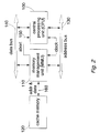
- the apparatus comprises a central processing unit (CPU) 100, a memory management unit (MMU) 110 and a random access memory (RAM) 120.
- the CPU 100 and the MMU 110 are linked by an address bus 130 for the exchange of memory addresses and a data bus 140 for the exchange of data.
- An abort control line 150 is also provided from the MMU 110 to the CPU 100 to carry an abort signal indicative of a failed or invalid memory access
- a clock signal is supplied to the CPU 100 and to the MMU 110 to control the operations of both of these units.
- Each data processing instruction is executed by the CPU 100 in a particular number of cycles of the clock signal (depending on the nature of that instruction) and memory access by the MMU 110 is performed in synchronism with the clock signal.
- the MMU 110 operates under the control of the CPU 100 and the clock signal to access data stored in the RAM 120. Accordingly, the MMU is linked to the RAM by a plurality of address and data lines 160.
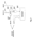
- FIG. 3 is a schematic block diagram of a part of the central processing unit 100.
- the CPU 100 employs instruction pipelining, to allow the processing and memory operations to be performed substantially continuously. Typically, while one data processing instruction is being executed, its successor is being decoded and a third instruction is being fetched from memory. This arrangement is referred to as a three-stage execution pipeline.
- data processing instructions which have been fetched from memory and then decoded are passed for execution.
- the data processing instructions are 32-bit data words, of which bits 28 to 31 form a 4-bit condition field.
- the remaining bits (bits 0 to 27) define the operation to be performed in response to that instruction and, in some cases an operand on which the operation is to be performed.
- condition field (bits 28 to 31) is passed to a condition tester 200 which compares the bits of the condition field with 16 predefined condition codes.
- the 16 condition codes define the state of one or more of four processor flags 210, referred to as the N, Z, C and V flags. These flags represent a processing state of the CPU 100 generated by previously executed instructions.
- the N flag denotes a negative result from the previous arithmetic operation of the CPU 100; the Z flag denotes a zero (equal) result from the previous CPU operation; the C flag denotes whether a carry bit was set during the previous CPU operation; and the V flag indicates an arithmetic overflow occurring during the previous CPU operation.
- the condition tester 200 tests the state of the flags listed above, in dependence on which bits are set in the condition field of the current instruction. This comparison takes place during execution of the current instruction. The current instruction is allowed to complete its execution only if the appropriate flags are set to the states specified by the condition field.
- the instruction will be executed irrespective of the flags.
- the never (NV) condition code prevents execution of the instruction irrespective of the state of the flags 210.
- the condition tester 200 generates an output signal 220 indicating whether the current instruction should be completely executed.
- the output signal 220 is combined with the abort signal supplied on the abort control line 150 from the MMU 110 to the CPU 100, using an OR-gate 230.
- the output of the OR-gate 230 is therefore set if either the condition tester 200 indicates that the current instruction should not be completely executed, or the abort signal is asserted by the MMU 110.
- An instruction execution unit 240 receives bits 0 to 27 of each instruction, defining the operation to be performed and, in some cases, an operand on which the operation is to be performed. During execution of the current instruction (i.e. after the propagation and processing delays of the condition tester 200 and the OR-gate 230), the instruction execution unit 240 receives the output of the OR-gate 230 indicating whether the current instruction should be completely executed. If the output of the OR-gate 230 indicates that the current instruction should not be completely executed, the instruction is cancelled without changing the state of any registers or memory locations associated with the apparatus.
- condition tester 200 and the instruction execution unit 240 may be of the same form as the corresponding components of the previously proposed ARM 6 processor referred to above.
- the result of using the apparatus of Figure 3 is that the stringent timing of the abort signal is greatly relaxed, so that the abort signal relating to a memory access initiated by the preceding instruction may be set at a late stage during execution of each instruction.
- Data read operations are followed by a non-memory-accessing (internal) processor cycle, to allow time for the data which has been read from memory to be loaded into the appropriate processor register. Accordingly, if an abort signal is received as a result of a failed data read operation, the internal cycle following the read operation allows time for any data supplied from memory by the MMU 110 (which data may well be erroneous) to be ignored and not stored in the intended location (e.g. a processor register).
- the MMU 110 which data may well be erroneous
- FIG. 4 The timing relationship of the instruction execution and the receipt of the abort signal for a data write operation is illustrated in Figure 4, in which a clock signal 300 which controls instruction execution by the CPU 100 is illustrated along with the states of the address bus 130 and the data bus 140.
- an address 310 is placed on the address bus by the CPU 100.
- data 320 are placed on the data bus 140 by the CPU 100. Once this has been done, the CPU 100 is able to execute the next instruction during the following cycle of the clock signal 300.
Description
- 0000 =
- EQ - Z set (equal)
- 0001 =
- NE - Z clear (not equal)
- 0010 =
- CS - C set (unsigned higher or same)
- 0011 =
- CC - C clear (unsigned lower)
- 0100 =
- MI - N set (negative)
- 0101 =
- PL - N clear (positive or zero)
- 0110 =
- VS - V set (overflow)
- 0111 =
- VC - V clear (no overflow)
- 1000 =
- HI - C set and Z clear (unsigned higher)
- 1001 =
- LS - C clear or Z set (unsigned lower or same)
- 1010 =
- GE - N set and V set, or N clear and V clear (greater or equal)
- 1011 =
- LT - N set and V clear, or N clear and V set (less than)
- 1100 =
- GT - Z clear, and either N set and V set, or N clear and V clear (greater than)
- 1101 =
- LE - Z set, or N set and V clear, or N clear and V set (less than or equal)
- 1110 =
- AL - always
- 1111 =
- NV - never
Claims (9)
- Data processing apparatus (100, 110, 120) in which successive data processing instructions are executed in a pipelined manner, said apparatus comprising:characterised by:memory accessing means (110) for accessing a data memory in response to one or more of said instructions, said memory accessing means comprising means for detecting whether each memory access is invalid; andcondition test means (200), responsive to a processing state of said apparatus generated by previously executed instructions and operable during execution of each Instruction, for detecting whether that instruction should be executed;
conditional control means (230, 240), responsive to said memory accessing means (110) and to said condition test means (200), for preventing complete execution of a current instruction if either said memory accessing means (110) detects that a memory access initiated by a preceding instruction is invalid or said condition test means (200) detects that said current instruction should not be executed. - Apparatus according to claim 1, in which:said apparatus comprises one or more processing flags (NZCV) for storing data indicative of a current processing state of said data processing apparatus;each instruction includes a condition code (bits 28 to 31) defining a state of said processing flags required for that instruction to be executed;said condition test means (200) is operable to compare a required state of the processing flags defined by said condition code in each instruction with an actual state of said processing flags.
- Apparatus according to claim 2, comprising four processing flags respectively denoting:(i) whether a previous data processing operation of said apparatus generated a negative result (N);(ii) whether a previous data processing operation of said apparatus generated a zero result (Z);(iii) whether a carry bit was set by a previous data processing operation of said apparatus (C); and(iv) whether an arithmetic overflow occurred during a previous data processing operation of said apparatus (V).
- Apparatus according to any one of claims 1 to 3, in which said memory accessing means (110) comprises:means for transmitting a memory address to said data memory (120); andmeans for subsequently transmitting data to said data memory or receiving data from said data memory.
- Apparatus according to any one of the preceding claims, in which:said memory accessing means (110) is operable to generate an abort control signal (150) to indicate that a memory access is invalid;said condition test means (200) is operable to generate a condition failure control signal (220) to indicate that said current instruction should not be executed; andsaid apparatus comprises means (230) for combining said abort control signal and said condition failure control signal to generate a combined control signal for supply to said condition control means (240).
- Apparatus according to claim 5, in which said means (230) for combining comprises a logical OR gate.
- Apparatus according to any one of the preceding claims, in which data processing operations of the apparatus are controlled by a clock signal.
- An integrated circuit comprising an apparatus according to any one of the preceding claims.
- A method of data processing in which successive data processing instructions are executed in a pipelined manner, said method comprising the steps of:characterised by the step of:accessing (110) a data memory in response to one or more of said instructions;detecting (110) whether each memory access is invalid; anddetecting (200), during execution of each instruction, whether that -instruction should be executed, in dependence on a processing state of said apparatus generated by previously executed instructions;
preventing (230, 240) complete execution of a current instruction if it is detected either that a memory access initiated by a preceding instruction is invalid or that said current instruction should not be executed.
Applications Claiming Priority (3)
| Application Number | Priority Date | Filing Date | Title |
|---|---|---|---|
| GB9319662 | 1993-09-23 | ||
| GB9319662A GB2282245B (en) | 1993-09-23 | 1993-09-23 | Execution of data processing instructions |
| PCT/GB1994/001793 WO1995008801A1 (en) | 1993-09-23 | 1994-08-16 | Execution of data processing instructions |
Publications (2)
| Publication Number | Publication Date |
|---|---|
| EP0721619A1 EP0721619A1 (en) | 1996-07-17 |
| EP0721619B1 true EP0721619B1 (en) | 1998-11-11 |
Family
ID=10742425
Family Applications (1)
| Application Number | Title | Priority Date | Filing Date |
|---|---|---|---|
| EP94923797A Expired - Lifetime EP0721619B1 (en) | 1993-09-23 | 1994-08-16 | Execution of data processing instructions |
Country Status (13)
| Country | Link |
|---|---|
| US (1) | US5961633A (en) |
| EP (1) | EP0721619B1 (en) |
| JP (1) | JP3553946B2 (en) |
| KR (1) | KR100335785B1 (en) |
| CN (1) | CN1099633C (en) |
| DE (1) | DE69414592T2 (en) |
| GB (1) | GB2282245B (en) |
| IL (1) | IL110799A (en) |
| IN (1) | IN189692B (en) |
| MY (1) | MY121544A (en) |
| RU (1) | RU2137182C1 (en) |
| TW (1) | TW332266B (en) |
| WO (1) | WO1995008801A1 (en) |
Families Citing this family (22)
| Publication number | Priority date | Publication date | Assignee | Title |
|---|---|---|---|---|
| JPH1049368A (en) * | 1996-07-30 | 1998-02-20 | Mitsubishi Electric Corp | Microporcessor having condition execution instruction |
| WO2004053685A1 (en) * | 2002-12-12 | 2004-06-24 | Arm Limited | Instruction timing control within a data processing system |
| US20040230781A1 (en) * | 2003-05-16 | 2004-11-18 | Via-Cyrix, Inc. | Method and system for predicting the execution of conditional instructions in a processor |
| US8056072B2 (en) | 2005-10-31 | 2011-11-08 | Microsoft Corporation | Rebootless display driver upgrades |
| US8880857B2 (en) | 2011-04-07 | 2014-11-04 | Via Technologies, Inc. | Conditional ALU instruction pre-shift-generated carry flag propagation between microinstructions in read-port limited register file microprocessor |
| US9645822B2 (en) | 2011-04-07 | 2017-05-09 | Via Technologies, Inc | Conditional store instructions in an out-of-order execution microprocessor |
| US9336180B2 (en) | 2011-04-07 | 2016-05-10 | Via Technologies, Inc. | Microprocessor that makes 64-bit general purpose registers available in MSR address space while operating in non-64-bit mode |
| US9128701B2 (en) | 2011-04-07 | 2015-09-08 | Via Technologies, Inc. | Generating constant for microinstructions from modified immediate field during instruction translation |
| EP2695077B1 (en) | 2011-04-07 | 2018-06-06 | VIA Technologies, Inc. | Conditional store instructions in an out-of-order execution microprocessor |
| US8924695B2 (en) | 2011-04-07 | 2014-12-30 | Via Technologies, Inc. | Conditional ALU instruction condition satisfaction propagation between microinstructions in read-port limited register file microprocessor |
| US9244686B2 (en) | 2011-04-07 | 2016-01-26 | Via Technologies, Inc. | Microprocessor that translates conditional load/store instructions into variable number of microinstructions |
| US9146742B2 (en) | 2011-04-07 | 2015-09-29 | Via Technologies, Inc. | Heterogeneous ISA microprocessor that preserves non-ISA-specific configuration state when reset to different ISA |
| US9292470B2 (en) | 2011-04-07 | 2016-03-22 | Via Technologies, Inc. | Microprocessor that enables ARM ISA program to access 64-bit general purpose registers written by x86 ISA program |
| US9378019B2 (en) | 2011-04-07 | 2016-06-28 | Via Technologies, Inc. | Conditional load instructions in an out-of-order execution microprocessor |
| US9898291B2 (en) | 2011-04-07 | 2018-02-20 | Via Technologies, Inc. | Microprocessor with arm and X86 instruction length decoders |
| US9043580B2 (en) | 2011-04-07 | 2015-05-26 | Via Technologies, Inc. | Accessing model specific registers (MSR) with different sets of distinct microinstructions for instructions of different instruction set architecture (ISA) |
| US9141389B2 (en) | 2011-04-07 | 2015-09-22 | Via Technologies, Inc. | Heterogeneous ISA microprocessor with shared hardware ISA registers |
| US9176733B2 (en) | 2011-04-07 | 2015-11-03 | Via Technologies, Inc. | Load multiple and store multiple instructions in a microprocessor that emulates banked registers |
| US8880851B2 (en) | 2011-04-07 | 2014-11-04 | Via Technologies, Inc. | Microprocessor that performs X86 ISA and arm ISA machine language program instructions by hardware translation into microinstructions executed by common execution pipeline |
| US9317288B2 (en) | 2011-04-07 | 2016-04-19 | Via Technologies, Inc. | Multi-core microprocessor that performs x86 ISA and ARM ISA machine language program instructions by hardware translation into microinstructions executed by common execution pipeline |
| US9274795B2 (en) | 2011-04-07 | 2016-03-01 | Via Technologies, Inc. | Conditional non-branch instruction prediction |
| US9032189B2 (en) | 2011-04-07 | 2015-05-12 | Via Technologies, Inc. | Efficient conditional ALU instruction in read-port limited register file microprocessor |
Family Cites Families (8)
| Publication number | Priority date | Publication date | Assignee | Title |
|---|---|---|---|---|
| BE789583A (en) * | 1971-10-01 | 1973-02-01 | Sanders Associates Inc | PROGRAM CONTROL APPARATUS FOR DATA PROCESSING MACHINE |
| GB1480209A (en) * | 1974-07-03 | 1977-07-20 | Data Loop Ltd | Digital computers |
| JPS54107645A (en) * | 1978-02-13 | 1979-08-23 | Hitachi Ltd | Information processor |
| JPS6247746A (en) * | 1985-08-27 | 1987-03-02 | Fujitsu Ltd | Interruption control system |
| JPH01229326A (en) * | 1988-03-09 | 1989-09-13 | Toshiba Corp | Information processor |
| JPH01310443A (en) * | 1988-06-09 | 1989-12-14 | Nec Corp | Information processor |
| US5202967A (en) * | 1988-08-09 | 1993-04-13 | Matsushita Electric Industrial Co., Ltd. | Data processing apparatus for performing parallel decoding and parallel execution of a variable word length instruction |
| JPH0335323A (en) * | 1989-06-30 | 1991-02-15 | Toshiba Corp | Control system for execution of instruction |
-
1993
- 1993-09-23 GB GB9319662A patent/GB2282245B/en not_active Expired - Fee Related
- 1993-10-16 TW TW082108586A patent/TW332266B/en not_active IP Right Cessation
-
1994
- 1994-08-16 WO PCT/GB1994/001793 patent/WO1995008801A1/en active IP Right Grant
- 1994-08-16 JP JP50961895A patent/JP3553946B2/en not_active Expired - Lifetime
- 1994-08-16 CN CN94194017A patent/CN1099633C/en not_active Expired - Lifetime
- 1994-08-16 US US08/619,647 patent/US5961633A/en not_active Expired - Lifetime
- 1994-08-16 KR KR1019960701507A patent/KR100335785B1/en not_active IP Right Cessation
- 1994-08-16 EP EP94923797A patent/EP0721619B1/en not_active Expired - Lifetime
- 1994-08-16 RU RU96107418A patent/RU2137182C1/en not_active IP Right Cessation
- 1994-08-16 DE DE69414592T patent/DE69414592T2/en not_active Expired - Lifetime
- 1994-08-28 IL IL110799A patent/IL110799A/en not_active IP Right Cessation
- 1994-08-30 IN IN1096DE1994 patent/IN189692B/en unknown
- 1994-09-09 MY MYPI94002370A patent/MY121544A/en unknown
Also Published As
| Publication number | Publication date |
|---|---|
| JP3553946B2 (en) | 2004-08-11 |
| KR100335785B1 (en) | 2002-11-30 |
| US5961633A (en) | 1999-10-05 |
| DE69414592D1 (en) | 1998-12-17 |
| WO1995008801A1 (en) | 1995-03-30 |
| CN1134193A (en) | 1996-10-23 |
| GB9319662D0 (en) | 1993-11-10 |
| EP0721619A1 (en) | 1996-07-17 |
| IN189692B (en) | 2003-04-12 |
| DE69414592T2 (en) | 1999-05-06 |
| CN1099633C (en) | 2003-01-22 |
| GB2282245B (en) | 1998-04-15 |
| GB2282245A (en) | 1995-03-29 |
| IL110799A (en) | 1997-09-30 |
| RU2137182C1 (en) | 1999-09-10 |
| KR960705271A (en) | 1996-10-09 |
| IL110799A0 (en) | 1994-11-11 |
| MY121544A (en) | 2006-02-28 |
| TW332266B (en) | 1998-05-21 |
| JPH09503876A (en) | 1997-04-15 |
Similar Documents
| Publication | Publication Date | Title |
|---|---|---|
| EP0721619B1 (en) | Execution of data processing instructions | |
| US4811215A (en) | Instruction execution accelerator for a pipelined digital machine with virtual memory | |
| US5127091A (en) | System for reducing delay in instruction execution by executing branch instructions in separate processor while dispatching subsequent instructions to primary processor | |
| EP0380846B1 (en) | Apparatus for resolving a variable number of potential memory access conflicts in a pipeline computer system and method therefor | |
| US4875160A (en) | Method for implementing synchronous pipeline exception recovery | |
| JP2539199B2 (en) | Digital processor controller | |
| US4982402A (en) | Method and apparatus for detecting and correcting errors in a pipelined computer system | |
| US5404552A (en) | Pipeline risc processing unit with improved efficiency when handling data dependency | |
| US4961162A (en) | Multiprocessing system for performing floating point arithmetic operations | |
| EP0394624B1 (en) | Multiple sequence processor system | |
| JPH0242569A (en) | Context switching method and apparatus used for vector processing system | |
| JPH0215369A (en) | Method and apparatus for executing instruction of vector processing system | |
| JP3707581B2 (en) | Data processing system having self-aligned stack pointer and method thereof | |
| EP0166431B1 (en) | An information processing apparatus having an instruction prefetch circuit | |
| EP0730228A1 (en) | ECC protected memory organization with pipelined read-modify-write accesses | |
| US5678016A (en) | Processor and method for managing execution of an instruction which determine subsequent to dispatch if an instruction is subject to serialization | |
| US5276822A (en) | System with enhanced execution of address-conflicting instructions using immediate data latch for holding immediate data of a preceding instruction | |
| US5287483A (en) | Prefetched operand storing system for an information processor | |
| US5732005A (en) | Single-precision, floating-point register array for floating-point units performing double-precision operations by emulation | |
| US6044460A (en) | System and method for PC-relative address generation in a microprocessor with a pipeline architecture | |
| US5784606A (en) | Method and system in a superscalar data processing system for the efficient handling of exceptions | |
| EP0415351A2 (en) | Data processor for processing instruction after conditional branch instruction at high speed | |
| EP0177712B1 (en) | Masked data fetch and modifying device | |
| JPH0418648A (en) | Data processor equipped with cache and data access method for the processor | |
| US5717891A (en) | Digital signal processor with caching of instructions that produce a memory conflict |
Legal Events
| Date | Code | Title | Description |
|---|---|---|---|
| PUAI | Public reference made under article 153(3) epc to a published international application that has entered the european phase |
Free format text: ORIGINAL CODE: 0009012 |
|
| 17P | Request for examination filed |
Effective date: 19960228 |
|
| AK | Designated contracting states |
Kind code of ref document: A1 Designated state(s): DE FR GB IT NL |
|
| GRAG | Despatch of communication of intention to grant |
Free format text: ORIGINAL CODE: EPIDOS AGRA |
|
| 17Q | First examination report despatched |
Effective date: 19980113 |
|
| GRAG | Despatch of communication of intention to grant |
Free format text: ORIGINAL CODE: EPIDOS AGRA |
|
| GRAH | Despatch of communication of intention to grant a patent |
Free format text: ORIGINAL CODE: EPIDOS IGRA |
|
| GRAH | Despatch of communication of intention to grant a patent |
Free format text: ORIGINAL CODE: EPIDOS IGRA |
|
| RAP1 | Party data changed (applicant data changed or rights of an application transferred) |
Owner name: ARM LIMITED |
|
| GRAA | (expected) grant |
Free format text: ORIGINAL CODE: 0009210 |
|
| AK | Designated contracting states |
Kind code of ref document: B1 Designated state(s): DE FR GB IT NL |
|
| REF | Corresponds to: |
Ref document number: 69414592 Country of ref document: DE Date of ref document: 19981217 |
|
| ET | Fr: translation filed | ||
| ITF | It: translation for a ep patent filed |
Owner name: MARIETTI E GISLON S.R.L. |
|
| PLBE | No opposition filed within time limit |
Free format text: ORIGINAL CODE: 0009261 |
|
| STAA | Information on the status of an ep patent application or granted ep patent |
Free format text: STATUS: NO OPPOSITION FILED WITHIN TIME LIMIT |
|
| 26N | No opposition filed | ||
| REG | Reference to a national code |
Ref country code: GB Ref legal event code: IF02 |
|
| PGFP | Annual fee paid to national office [announced via postgrant information from national office to epo] |
Ref country code: IT Payment date: 20060831 Year of fee payment: 13 |
|
| PG25 | Lapsed in a contracting state [announced via postgrant information from national office to epo] |
Ref country code: IT Free format text: LAPSE BECAUSE OF NON-PAYMENT OF DUE FEES Effective date: 20070816 |
|
| PGFP | Annual fee paid to national office [announced via postgrant information from national office to epo] |
Ref country code: DE Payment date: 20130814 Year of fee payment: 20 Ref country code: NL Payment date: 20130810 Year of fee payment: 20 |
|
| PGFP | Annual fee paid to national office [announced via postgrant information from national office to epo] |
Ref country code: GB Payment date: 20130814 Year of fee payment: 20 Ref country code: FR Payment date: 20130808 Year of fee payment: 20 |
|
| REG | Reference to a national code |
Ref country code: DE Ref legal event code: R071 Ref document number: 69414592 Country of ref document: DE |
|
| REG | Reference to a national code |
Ref country code: NL Ref legal event code: V4 Effective date: 20140816 |
|
| REG | Reference to a national code |
Ref country code: GB Ref legal event code: PE20 Expiry date: 20140815 |
|
| PG25 | Lapsed in a contracting state [announced via postgrant information from national office to epo] |
Ref country code: DE Free format text: LAPSE BECAUSE OF EXPIRATION OF PROTECTION Effective date: 20140819 |
|
| PG25 | Lapsed in a contracting state [announced via postgrant information from national office to epo] |
Ref country code: GB Free format text: LAPSE BECAUSE OF EXPIRATION OF PROTECTION Effective date: 20140815 |