EP0720228A2 - Semiconductor connection structure and method - Google Patents
Semiconductor connection structure and method Download PDFInfo
- Publication number
- EP0720228A2 EP0720228A2 EP95308801A EP95308801A EP0720228A2 EP 0720228 A2 EP0720228 A2 EP 0720228A2 EP 95308801 A EP95308801 A EP 95308801A EP 95308801 A EP95308801 A EP 95308801A EP 0720228 A2 EP0720228 A2 EP 0720228A2
- Authority
- EP
- European Patent Office
- Prior art keywords
- layer
- conductive material
- conductive
- opening
- barrier metal
- Prior art date
- Legal status (The legal status is an assumption and is not a legal conclusion. Google has not performed a legal analysis and makes no representation as to the accuracy of the status listed.)
- Granted
Links
Images


Classifications
-
- H—ELECTRICITY
- H01—ELECTRIC ELEMENTS
- H01L—SEMICONDUCTOR DEVICES NOT COVERED BY CLASS H10
- H01L21/00—Processes or apparatus adapted for the manufacture or treatment of semiconductor or solid state devices or of parts thereof
- H01L21/70—Manufacture or treatment of devices consisting of a plurality of solid state components formed in or on a common substrate or of parts thereof; Manufacture of integrated circuit devices or of parts thereof
- H01L21/71—Manufacture of specific parts of devices defined in group H01L21/70
- H01L21/768—Applying interconnections to be used for carrying current between separate components within a device comprising conductors and dielectrics
- H01L21/76838—Applying interconnections to be used for carrying current between separate components within a device comprising conductors and dielectrics characterised by the formation and the after-treatment of the conductors
- H01L21/76841—Barrier, adhesion or liner layers
- H01L21/76843—Barrier, adhesion or liner layers formed in openings in a dielectric
- H01L21/76849—Barrier, adhesion or liner layers formed in openings in a dielectric the layer being positioned on top of the main fill metal
-
- H—ELECTRICITY
- H01—ELECTRIC ELEMENTS
- H01L—SEMICONDUCTOR DEVICES NOT COVERED BY CLASS H10
- H01L21/00—Processes or apparatus adapted for the manufacture or treatment of semiconductor or solid state devices or of parts thereof
- H01L21/70—Manufacture or treatment of devices consisting of a plurality of solid state components formed in or on a common substrate or of parts thereof; Manufacture of integrated circuit devices or of parts thereof
- H01L21/71—Manufacture of specific parts of devices defined in group H01L21/70
- H01L21/768—Applying interconnections to be used for carrying current between separate components within a device comprising conductors and dielectrics
- H01L21/76838—Applying interconnections to be used for carrying current between separate components within a device comprising conductors and dielectrics characterised by the formation and the after-treatment of the conductors
- H01L21/76841—Barrier, adhesion or liner layers
- H01L21/76853—Barrier, adhesion or liner layers characterized by particular after-treatment steps
- H01L21/76865—Selective removal of parts of the layer
-
- H—ELECTRICITY
- H01—ELECTRIC ELEMENTS
- H01L—SEMICONDUCTOR DEVICES NOT COVERED BY CLASS H10
- H01L21/00—Processes or apparatus adapted for the manufacture or treatment of semiconductor or solid state devices or of parts thereof
- H01L21/70—Manufacture or treatment of devices consisting of a plurality of solid state components formed in or on a common substrate or of parts thereof; Manufacture of integrated circuit devices or of parts thereof
- H01L21/71—Manufacture of specific parts of devices defined in group H01L21/70
- H01L21/768—Applying interconnections to be used for carrying current between separate components within a device comprising conductors and dielectrics
- H01L21/76838—Applying interconnections to be used for carrying current between separate components within a device comprising conductors and dielectrics characterised by the formation and the after-treatment of the conductors
- H01L21/76877—Filling of holes, grooves or trenches, e.g. vias, with conductive material
- H01L21/76879—Filling of holes, grooves or trenches, e.g. vias, with conductive material by selective deposition of conductive material in the vias, e.g. selective C.V.D. on semiconductor material, plating
-
- H—ELECTRICITY
- H01—ELECTRIC ELEMENTS
- H01L—SEMICONDUCTOR DEVICES NOT COVERED BY CLASS H10
- H01L21/00—Processes or apparatus adapted for the manufacture or treatment of semiconductor or solid state devices or of parts thereof
- H01L21/70—Manufacture or treatment of devices consisting of a plurality of solid state components formed in or on a common substrate or of parts thereof; Manufacture of integrated circuit devices or of parts thereof
- H01L21/71—Manufacture of specific parts of devices defined in group H01L21/70
- H01L21/768—Applying interconnections to be used for carrying current between separate components within a device comprising conductors and dielectrics
- H01L21/76838—Applying interconnections to be used for carrying current between separate components within a device comprising conductors and dielectrics characterised by the formation and the after-treatment of the conductors
- H01L21/76885—By forming conductive members before deposition of protective insulating material, e.g. pillars, studs
-
- H—ELECTRICITY
- H01—ELECTRIC ELEMENTS
- H01L—SEMICONDUCTOR DEVICES NOT COVERED BY CLASS H10
- H01L23/00—Details of semiconductor or other solid state devices
- H01L23/52—Arrangements for conducting electric current within the device in operation from one component to another, i.e. interconnections, e.g. wires, lead frames
- H01L23/522—Arrangements for conducting electric current within the device in operation from one component to another, i.e. interconnections, e.g. wires, lead frames including external interconnections consisting of a multilayer structure of conductive and insulating layers inseparably formed on the semiconductor body
- H01L23/5226—Via connections in a multilevel interconnection structure
-
- H—ELECTRICITY
- H01—ELECTRIC ELEMENTS
- H01L—SEMICONDUCTOR DEVICES NOT COVERED BY CLASS H10
- H01L23/00—Details of semiconductor or other solid state devices
- H01L23/52—Arrangements for conducting electric current within the device in operation from one component to another, i.e. interconnections, e.g. wires, lead frames
- H01L23/522—Arrangements for conducting electric current within the device in operation from one component to another, i.e. interconnections, e.g. wires, lead frames including external interconnections consisting of a multilayer structure of conductive and insulating layers inseparably formed on the semiconductor body
- H01L23/532—Arrangements for conducting electric current within the device in operation from one component to another, i.e. interconnections, e.g. wires, lead frames including external interconnections consisting of a multilayer structure of conductive and insulating layers inseparably formed on the semiconductor body characterised by the materials
- H01L23/53204—Conductive materials
- H01L23/53209—Conductive materials based on metals, e.g. alloys, metal silicides
- H01L23/53214—Conductive materials based on metals, e.g. alloys, metal silicides the principal metal being aluminium
- H01L23/53223—Additional layers associated with aluminium layers, e.g. adhesion, barrier, cladding layers
-
- H—ELECTRICITY
- H01—ELECTRIC ELEMENTS
- H01L—SEMICONDUCTOR DEVICES NOT COVERED BY CLASS H10
- H01L2924/00—Indexing scheme for arrangements or methods for connecting or disconnecting semiconductor or solid-state bodies as covered by H01L24/00
- H01L2924/0001—Technical content checked by a classifier
- H01L2924/0002—Not covered by any one of groups H01L24/00, H01L24/00 and H01L2224/00
Definitions
- the present invention relates generally to semiconductor devices, and more specifically to a structure and method for forming electrical connections between levels of a semiconductor device.
- interconnection layer of aluminum which is highly conductive while being relatively easy to deposit and etch, for connecting different elements of the integrated circuit to each other.
- This layer usually rests on an insulating layer which in turn is located above a conductive layer.
- the insulating layer is opened prior to deposition of the aluminum in order to expose the conductive layer surfaces with which to establish a metallic interconnection.
- These conductive surfaces can be monocrystalline silicon surfaces (transistor sources, drains, collectors, bases and emitters), polycrystalline silicon elements (field-effect transistor gates) or metallic surfaces of another interconnection layer.
- the contact opening is initially filled or "plugged" with a metallic layer, such as aluminum or tungsten, to make a solid electrical connection between the underlying conductive layer and the overlying interconnection aluminum layer.
- tungsten encroachment or "worm-holing."
- Tungsten and silicon do not readily react at typical metallization temperatures of less than 500°C.
- the CVD of tungsten is performed using WF 6 and the fluorine in WF 6 reacts with silicon in the presence of tungsten which acts as a catalyst in the reaction. This tungsten encroachment problem is well-known in the art and widely reported in industry literatures.
- a barrier metal layer such as TiN solves this problem by preventing fluorine from contacting silicon surfaces.
- barrier metal is needed only at the bottom of the contact opening to prevent the tungsten encroachment problem, it is still necessary, or at least desirable, to deposit the barrier metal on the sidewalls of the contact opening as well. This is because CVD tungsten does not readily deposit on or adhere to an insulating layer such as SiO 2 . Since the contact opening sidewalls are part of the insulating layer, a continuous barrier metal layer on the sidewalls is helpful to ensure conformal deposition of tungsten required to form a complete plug within the contact opening.
- Tungsten for example, is selectively etched with fluorine ions over titanium, titanium nitride, and aluminum.
- titanium, titanium nitride, and aluminum are selectively etched with chlorine ions relative to tungsten. Because of this etching selectivity, the tungsten plug within the contact opening can be etched back very uniformly and completely using titanium nitride, a barrier metal, as an etch stop. Then during the formation of an aluminum interconnection layer, for example, the tungsten plug is used as an etch stop for the aluminum.
- This aluminum etch process is relatively long due to the need to remove residual aluminum and titanium nitride over topographical steps, where they are more difficult to etch.
- the chlorine etch preferred for etching aluminum also etches barrier metals such as titanium or titanium nitride.
- barrier metals such as titanium or titanium nitride.
- the barrier metal between the sidewall and the tungsten plug will also be etched when aluminum is etched. Because the etching period and over etch period for the aluminum metal is relatively long, the barrier metal on the sidewall can erode partially even towards the bottom of the contact opening. This may destroy the underlying conductive region such as a transistor source or drain located underneath the tungsten plug.
- One method of preventing this problem is to make the interconnection layer of aluminum sufficiently large over the plug so that it completely covers and encloses the tungsten plug.
- a minimum enclosure defines the extra surface area which must be added to an interconnection layer in order to compensate for mask misalignment and other process variations.
- the widened portion over the plug may be typically approximately twice the interconnection layer width for small geometry devices. This enlarged area is designed to be centered on the interconnection layer, but it may be offset to one side and made sufficiently large to compensate for mask misalignment and other process variations. For example, if an interconnection layer has a width of 1 micron, the width of the region overlying the contact opening might be 2.0 microns to ensure complete coverage and enclosure of the tungsten plug and titanium sidewall.
- interconnection layers may be only 0.4-0.5 micron wide and stacked three to five levels deep.
- an electrical connection structure and method are provided for protecting a barrier metal layer within the contact opening during the formation of an interconnection layer overlying the contact opening.
- Conductive layer regions of integrated circuit elements are formed above a semiconductor substrate.
- An insulating layer is deposited over those conductive layers.
- a contact opening is etched through the insulating layer exposing a portion of the underlying conductive layer.
- a thin layer of a barrier metal is deposited on the insulating layer which results in deposition of the barrier metal on the exposed area of the underlying conductive layer and the sidewalls of the contact opening.
- a conductive material such as tungsten is deposited to a sufficient thickness to fill the opening. Then the deposited conductive material is etched back without a mask until the barrier metal on the insulating layer is exposed.
- the deposited conductive material is etched back further in order to create a slight recess below the contact opening. This will expose an upper portion of the thin barrier metal layer on the sidewalls of the opening.
- the next step is to etch the thin layer of the barrier metal on the insulating layer and the exposed barrier metal within the opening. This step may create a slight erosion of the barrier metal layer between the conductive material and sidewalls near the top of the conductive material.
- conductive material is selectively deposited. The selective deposition of the conductive material covers the contact opening and protects the thin layer of the barrier metal on the sidewalls and the bottom surface of the contact opening from subsequent etch steps.
- an aluminum interconnection layer over a selectively deposited tungsten aluminum is selectively etched over tungsten, the tungsten acting as an etch stop. Since the barrier metal layer is covered by the selectively deposited tungsten, the aluminum etchant does not come in contact with the barrier metal layer and it is not etched.
- an electrical connection structure in integrated circuit devices comprising a first conductive layer, an insulating layer overlying the conductive layer, the insulating layer having an upper surface, an opening through the insulating layer and exposing a region of the conductive layer, the opening having sidewalls, a thin layer of a barrier material covering the exposed conductive layer region and only a portion of the sidewalls such that the upper portion of the sidewalls is not covered by the barrier metal, a first conductive material filling the opening over the thin layer of the barrier metal to a level below the insulating layer inner surface, and a layer of a second conductive material positioned over the first conductive material layer and the exposed barrier metal, the layer of the second conductive material having an upper surface approximately co-planar with the insulating layer upper surface.
- the thin layer of the barrier material may be either titanium, or titanium nitride, or titanium nitride on titanium bilayer.
- the conductive layer may be an integrated circuit element or polysilicon.
- the conductive layer may be an interconnection layer to other integrated circuit elements.
- the lateral dimension of the opening may be approximately one micron for an insulating layer having a thickness in the range of one to four microns.
- the thickness of the second conductive material layer may range from one hundred angstrom to one thousand angstrom.
- the second conductive material may be tungsten.
- the layer of the second conductive material may be formed by chemical vapor deposition with a relatively high H 2 to WF 6 flow ratio.
- the H 2 to WF 6 flow ratio may range from 5 to 20.
- the first and second conductive materials may both be tungsten.
- the second conductive material may be aluminium.
- an electrical connection structure in integrated circuit devices comprising a first conductive layer, an insulating layer overlying the conductive layer, the insulating layer having an upper surface, an opening through the insulating layer and exposing a region of the conductive layer, the opening having sidewalls, a first conductive material filling the opening to a level below the insulating layer upper surface, a layer of a second conductive material positioned over the first conductive material layer; the layer of the second conductive material having an upper surface approximately co-planar with the insulating layer upper surface, and an interconnection layer overlying the second conductive material layer, the second conductive material and interconnection layer being selected with respect to each other such that the second conductive layer is an etch stop for the etching of the interconnection layer.
- a method of forming an electrical connection structure in integrated circuit devices comprising the steps of forming a conductive layer, forming an insulating layer overlying the conductive layer, etching an opening through the insulating layer and exposing a region of the conductive layer; the opening having sidewalls, depositing a thin layer of a barrier metal overlying the sidewalls and the exposed conductive layer region prior to depositing the first conductive material and, depositing a first conductive material over the thin layer of the barrier metal of sufficient thickness to fill the opening, etching the deposited first conductive material sufficiently to create a slight recess at the opening, etching the barrier metal from the upper surface of the insulating layer and from an upper portion of the sidewalls of the opening to form a recess, and filling the recess in the opening by selectively depositing a second conductive material overlying the first conductive material and the thin layer of the barrier metal, and contacting the sidewalls of the opening such that
- the second conductive material may be tungsten.
- the step of filling the recess may include the step of selectively depositing tungsten by chemical vapor deposition with a relatively high H 2 to WF 6 flow ratio.
- the H 2 to WF 6 flow ratio may range from 5 to 20.
- the first and second conductive materials may both be tungsten.
- the thickness of the selectively deposited second conductive material may range from one hundred angstrom to one thousand angstrom.
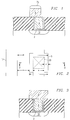
- FIG. 1 illustrates the problem recognized by applicants.
- a photoresist 26 used to pattern an interconnection layer 6 may be misaligned with an underlying connection area.
- a deposited metal plug 4 such as tungsten is used as an etch stop. Because the photoresist 26 is misaligned with the metal plug 4, the exposed barrier metal 2 is etched along with aluminum 6. The barrier metal layer 2 erodes along the sidewall of the contact opening as shown. This will result in poor electrical contact between the interconnection layer 6 and an underlying conductive layer region 10. It is common in the art to overetch during an aluminum etching process due to the need to remove residual aluminum and barrier metal.
- the erosion of the barrier metal 2 may continue all the way down the sidewall and onto a portion of the conductive layer 10 destroying the associated electrical circuit.
- the etch does not remove the titanium to the layer 10, it may still be etched from the sidewall sufficient to cause the plug 4 to move in the hole and create electrical problems.
- FIG. 2 shows a plan view of a prior art interconnection layer 6 formed over a contact opening 30 for preventing the side erosion problem by using the enclosure rule discussed above.
- a widened portion of the interconnection layer 6 is centered over the contact opening 30.
- a second interconnection layer 12 runs alongside the first layer 6. While the width of the interconnection layer is only w, extra width of e must be added to each side to the layer 6 to compensate for a maximum misalignment of e to either side of the contact opening 30. This will increase the pitch p (width of interconnection layer i + spacing s) between interconnection layers 6, 12 at the level of contact openings resulting in waste of valuable layout space.
- FIG. 3 is a cross-sectional view of the prior art interconnection layer 6 taken along lines 3-3 of FIG. 2.
- the enclosure requirements reduce the density of interconnection layers 6, 12 that can be formed over the insulating layer 8 since each layer has a portion with a widened area.
- FIGS. 4A through 4I show a presently preferred method of protecting a liner material layer 2 during formation of an interconnection layer 6 overlying a contact opening 30.
- a semiconductor substrate 14 contains a conductive layer region 10 to which electrical contact is desired (FIG. 4A).
- the layer 14 is an interconnection layer of itself, either of polysilicon or metal.
- An insulating layer of silicon dioxide 8 overlies the substrate 14.
- a contact opening 30 is made through the insulating layer 8. Over that insulating layer 8 and in the opening 30, a thin layer 2 of a barrier metal is deposited.
- the liner material 2 which is deposited inside the contact opening 30 is preferably a barrier metal, such as titanium, titanium nitride, or titanium nitride on titanium bilayer.
- barrier metal/barrier metal compound/barrier metal may also be used, such as Ti/TiN/Ti.
- any material, whether metal or semi-metal which can be selectively etched over the connection plug material 22 can be used.
- the deposition can be done either by sputtering the barrier metal 2 or alternatively by a relatively new process of barrier metal CVD although the CVD method limits the choice of a barrier metal to titanium nitride.
- This barrier metal layer 2 can have a thickness in the range of from approximately 100 ⁇ to more than 3,000 ⁇ , depending on the design requirements.
- a conductive material 20 is conformally deposited preferably by using a CVD (FIG. 4B).
- the conductive material 20 is tungsten.
- the conductive material 20 is aluminum or other highly conductive material that is conformally deposited.
- the deposited conductive material 20 is then etched back without a mask. The etch continues until the barrier metal layer 2 on the insulating layer 8 is exposed. Then for a controlled amount of time, the material 20 inside the contact opening 30 is etched further to create the desired level of recess 31 below the opening 30 (FIG. 4C).
- the depth of the recess is preferably in the range of 50 ⁇ to 1000 ⁇ for reasons discussed later herein.
- the etch is terminated and the barrier metal layer 2 is etched.
- Many acceptable etching techniques for the barrier metal are known; one acceptable technique is a plasma etch using chlorine ions until the insulating layer 8 is exposed (FIG. 4D).
- An etch that is selective to the barrier metal over the tungsten plug is preferred. In this etching process, a slight recess 33 of the barrier metal layer 2 on the sidewalls of the opening 30 may be created, but is not necessary, as shown in FIG. 4D.
- a selective tungsten deposition is then performed for filling the recesses 31 (and 33 if present) within the contact opening 30 (FIG. 4E).
- This selective tungsten deposition is performed without a mask.
- the deposition chemistry is selected such that tungsten will selectively deposit on the plug 20 but not on the insulator 8.
- Deposition chemistry to perform selective tungsten deposition on tungsten or other materials, such as aluminum, is known in the art, having been described in published literature.
- One preferred process is a chemical vapor deposition process in which, WF 6 and H 2 are introduced with a relatively high H 2 to WF 6 flow ratio to deposit tungsten onto tungsten.
- the flow ratio is in the range of 10 to 20 more H 2 than WF 6 .
- tungsten 22 Under this environment, up to a 1000 ⁇ of tungsten 22 will be selectively deposited on the exposed tungsten surface 20 before being deposited on other surfaces.
- This etch stop layer 22 of tungsten 22 protects the underlying barrier metal layer 2 on the sidewalls and the conductive layer region 10, and also acts as an complete etch stop for chlorine ions which will later be used to etch an aluminum interconnection layer 6.
- the depth of the recess 31 is selected to be sufficiently deep that a protective tungsten layer is formed, but not so deep that selective deposition onto only tungsten is not easily achieved. Thus, the range of 50 ⁇ to 1000 ⁇ is preferred based on today's technologies. A mask and etch step is not required, thus simplifying the process.
- an aluminum interconnection layer 6 over a selectively deposited tungsten 22 aluminum 6 is blanket deposited over the insulating layer 8.
- a photoresist pattern 26 is then placed over selected regions of aluminum (FIG. 4G).
- the regions of the deposited aluminum which are not covered by the photoresist 26 are selectively etched over tungsten 22 which acts as an etch stop (FIG. 4H).
- the photoresist feature 26 may be misaligned, as shown. Since the barrier metal layer 2 is covered by the selectively deposited tungsten 22, the aluminum etchant does not come in contact with the barrier metal layer 2.
- the etch stop layer 22 is not aluminum.
- the material of layer 22 is selected to be an etch stop for the etching of interconnection layer 6.
- the plug 20 is formed of tungsten
- the cap layer 22 is tungsten
- the interconnection layer 6 is aluminum.
- the plug 20 is aluminum
- the stop layer 22 is tungsten
- the interconnection layer 6 is aluminum.
- the conductive layer 10 is compatible with the plug material 20
- no liner layer 2 is used.
- the conductive layer 10 may be aluminum and the plug 20 is aluminum so that no liner layer 2 is needed.
- the interconnection layer 6 is also aluminum.
- the etch stop layer 22 is formed as previously described using an etch stop material for an aluminum etch such as tungsten, as the layer 22.
- a conductive cap layer 24 is optionally placed between the interconnection layer 6 and the connection structure 2, 20, 22 in one embodiment.
- the cap layer 24 is blanket deposited before the blanket deposition of the layer 6 as shown in FIG. 4G.
- the aluminum is then blanket deposited over the cap layer 24 and a single mask is used to etch both layers.
- the cap layer 24 is used for improving the interface chemistry at the contact level. This includes lower electrical resistance at the interface, and better adhesion between the interconnection layer 6 and the connection structure 2, 20, 22. Since the desired properties of a cap layer 24 are similar to those of barrier metal, any barrier metal discussed above would also be suitable as the cap layer 24.
- connection structure 2, 20, 22 allows for this type of misalignment since the barrier metal 2 along the sidewalls of the opening 30 is fully protected from the etching chemical used to pattern the interconnection layer 6. Since there is no widened portion of the interconnection layer 6 over the connection structure 2, 20, 22, a second interconnection layer 10 can be placed much closer to the first layer 6 as compared to those in FIG. 2. As can be seen, the pitch p' in FIG. 6 is much shorter than the pitch p in FIG. 2, which allows the electrical circuits and interconnection layers 6, 10 to be more tightly packed than was previously possible.
- connection plug structure described herein is illustrated as making a contact to a conductive region of an underlying silicon substrate.
- the same techniques can be used to fabricate a connection structure between an upper interconnection layer and an underlying polycrystalline silicon interconnect, or between two metal interconnection layers.
Abstract
Description
- The present invention relates generally to semiconductor devices, and more specifically to a structure and method for forming electrical connections between levels of a semiconductor device.
- It is a common practice in the fabrication of integrated circuits to make use of an interconnection layer of aluminum, which is highly conductive while being relatively easy to deposit and etch, for connecting different elements of the integrated circuit to each other. This layer usually rests on an insulating layer which in turn is located above a conductive layer. The insulating layer is opened prior to deposition of the aluminum in order to expose the conductive layer surfaces with which to establish a metallic interconnection. These conductive surfaces can be monocrystalline silicon surfaces (transistor sources, drains, collectors, bases and emitters), polycrystalline silicon elements (field-effect transistor gates) or metallic surfaces of another interconnection layer. The contact opening is initially filled or "plugged" with a metallic layer, such as aluminum or tungsten, to make a solid electrical connection between the underlying conductive layer and the overlying interconnection aluminum layer.
- However, problems occur with aluminum contacts on silicon because of interdiffusion of aluminum in later process steps and degrading over time. Aluminum may also create spiking in the silicon. To prevent spiking and alloying between an aluminum interconnection metal and silicon surface, a thin "barrier" or "seed" metal layer is deposited on the exposed silicon surface of the contact opening prior to plugging the opening with aluminum. The most useful and practical barrier metal has been a titanium, or titanium nitride on titanium (TiN/Ti) bilayer which deposits well on silicon and silicon dioxide surfaces and also acts as glue for metal plugs of tungsten on silicon surfaces. The TiN/Ti scheme, however, has some drawbacks. It does not deposit easily and uniformly on the vertical sidewalls of an opening and the thickness on the bottom is a small fraction of that on the surface outside the contacts when spattering or physical vapor deposition is used. The bottom and sidewall coverage is especially important in "hot aluminum plug" processing in order to facilitate the surface diffusion of aluminum atoms into the contact opening and to withstand an even greater tendency for spiking due to the high aluminum deposition temperature. In order to ensure adequate deposition of the barrier film on the bottom and sidewalls of a contact opening for such aluminum plugs, it was previously necessary to step down the contact opening as shown in the prior art for U.S. patent No. 4,592,802 and U.S. patent No. 5,231,051. However, such steps of the contact opening uses valuable layout space of a silicon structure.
- This problem is partly solved by the use of chemical vapor deposition (CVD) tungsten etched back plug, a process well-known in the art and described in U.S. Patent Nos. 4,592,802 and 5,231,051, both of which are incorporated herein by reference. In this process, the contact opening is filled with tungsten to a level above the insulating layer to make sure the opening is completely filled. The deposited tungsten is then etched back without a mask until the insulating layer is exposed. Because CVD of tungsten is generally conformal, i.e., the deposition rate on vertical surfaces is generally the same as that on horizontal surfaces, this method produces a complete plug in the opening. By using this method, a barrier metal layer is no longer needed to prevent the problem of spiking between an aluminum plug and silicon.
- Despite the success achieved with tungsten plugs in preventing spiking, however, it is still desirable to have a barrier metal layer at the bottom of the contact opening. The barrier layer underlying the tungsten plug is desired not because of the spiking problem as in the case of aluminum, but because of a quite different phenomenon known as "tungsten encroachment" or "worm-holing." Tungsten and silicon do not readily react at typical metallization temperatures of less than 500°C. However, the CVD of tungsten is performed using WF6 and the fluorine in WF6 reacts with silicon in the presence of tungsten which acts as a catalyst in the reaction. This tungsten encroachment problem is well-known in the art and widely reported in industry literatures. A barrier metal layer such as TiN solves this problem by preventing fluorine from contacting silicon surfaces.
- while the barrier metal is needed only at the bottom of the contact opening to prevent the tungsten encroachment problem, it is still necessary, or at least desirable, to deposit the barrier metal on the sidewalls of the contact opening as well. This is because CVD tungsten does not readily deposit on or adhere to an insulating layer such as SiO2. Since the contact opening sidewalls are part of the insulating layer, a continuous barrier metal layer on the sidewalls is helpful to ensure conformal deposition of tungsten required to form a complete plug within the contact opening.
- Hence, regardless of which metal (aluminum or tungsten) is used as a connection plug, the need for a continuous barrier metal layer on the sidewalls, especially in large aspect ratio contact openings, now about 3.5:1 to as much as 5:1 for advanced integrated circuits, is still present. Because of this, the industry has expended a great deal of effort in achieving conformal deposition of barrier metal in the contact opening. To this end, integrated circuit processing industry has recently developed a CVD of TiN process which provides good sidewall coverage of the contact opening and most manufacturers are moving toward CVD of TiN.
- However, a good consistent barrier film in the contact opening which affords good adhesion to all surfaces and prevents encroachment at the bottom of contact openings presents a new difficulty. It is possible, in some instances, due to mask misalignment and other process variations, that a metallic interconnection layer over a metal tungsten plug in the contact opening fails to completely cover every portion of that opening. In those cases, during etching of the metallic interconnection layer, the barrier metal exposed to the etching chemical will also be etched, which results in void formation or even spiking along the sidewalls of the contact opening.
- Selective etching of tungsten relative to aluminum or titanium is easy to achieve. Tungsten, for example, is selectively etched with fluorine ions over titanium, titanium nitride, and aluminum. In addition, titanium, titanium nitride, and aluminum are selectively etched with chlorine ions relative to tungsten. Because of this etching selectivity, the tungsten plug within the contact opening can be etched back very uniformly and completely using titanium nitride, a barrier metal, as an etch stop. Then during the formation of an aluminum interconnection layer, for example, the tungsten plug is used as an etch stop for the aluminum. This aluminum etch process is relatively long due to the need to remove residual aluminum and titanium nitride over topographical steps, where they are more difficult to etch.
- The problem recognized by applicants is that the chlorine etch preferred for etching aluminum also etches barrier metals such as titanium or titanium nitride. As a result, the barrier metal between the sidewall and the tungsten plug will also be etched when aluminum is etched. Because the etching period and over etch period for the aluminum metal is relatively long, the barrier metal on the sidewall can erode partially even towards the bottom of the contact opening. This may destroy the underlying conductive region such as a transistor source or drain located underneath the tungsten plug.
- One method of preventing this problem is to make the interconnection layer of aluminum sufficiently large over the plug so that it completely covers and encloses the tungsten plug. A minimum enclosure defines the extra surface area which must be added to an interconnection layer in order to compensate for mask misalignment and other process variations. The widened portion over the plug may be typically approximately twice the interconnection layer width for small geometry devices. This enlarged area is designed to be centered on the interconnection layer, but it may be offset to one side and made sufficiently large to compensate for mask misalignment and other process variations. For example, if an interconnection layer has a width of 1 micron, the width of the region overlying the contact opening might be 2.0 microns to ensure complete coverage and enclosure of the tungsten plug and titanium sidewall. It is clearly disadvantageous to have wider interconnection layers or enlarged regions over a contact, especially in today's integrated circuit devices in which the circuit elements and interconnection layers are packed more tightly than ever before; in today's 0.35 micron technology devices, for example, the interconnection layers may be only 0.4-0.5 micron wide and stacked three to five levels deep.
- Thus, it would be desirable to provide a contact opening that is not subject to erosion during formation of an interconnection layer. It would also be desirable to do this in such a way as to preserve much of the barrier metal deposited on the sidewalls so that deposition of a metal plug within the opening is conformal.
- According to principles of the present invention, an electrical connection structure and method are provided for protecting a barrier metal layer within the contact opening during the formation of an interconnection layer overlying the contact opening.
- Conductive layer regions of integrated circuit elements are formed above a semiconductor substrate. An insulating layer is deposited over those conductive layers. A contact opening is etched through the insulating layer exposing a portion of the underlying conductive layer. To form a connection plug, a thin layer of a barrier metal is deposited on the insulating layer which results in deposition of the barrier metal on the exposed area of the underlying conductive layer and the sidewalls of the contact opening. Over the thin barrier metal layer in the opening, a conductive material such as tungsten is deposited to a sufficient thickness to fill the opening. Then the deposited conductive material is etched back without a mask until the barrier metal on the insulating layer is exposed. For a controlled period of time thereafter, the deposited conductive material is etched back further in order to create a slight recess below the contact opening. This will expose an upper portion of the thin barrier metal layer on the sidewalls of the opening. The next step is to etch the thin layer of the barrier metal on the insulating layer and the exposed barrier metal within the opening. This step may create a slight erosion of the barrier metal layer between the conductive material and sidewalls near the top of the conductive material. Within the recess and on the exposed barrier metal layer, conductive material is selectively deposited. The selective deposition of the conductive material covers the contact opening and protects the thin layer of the barrier metal on the sidewalls and the bottom surface of the contact opening from subsequent etch steps. For example, during the formation of an aluminum interconnection layer over a selectively deposited tungsten, aluminum is selectively etched over tungsten, the tungsten acting as an etch stop. Since the barrier metal layer is covered by the selectively deposited tungsten, the aluminum etchant does not come in contact with the barrier metal layer and it is not etched.
- According to a first aspect of the present invention there is provided an electrical connection structure in integrated circuit devices comprising a first conductive layer, an insulating layer overlying the conductive layer, the insulating layer having an upper surface, an opening through the insulating layer and exposing a region of the conductive layer, the opening having sidewalls, a thin layer of a barrier material covering the exposed conductive layer region and only a portion of the sidewalls such that the upper portion of the sidewalls is not covered by the barrier metal, a first conductive material filling the opening over the thin layer of the barrier metal to a level below the insulating layer inner surface, and a layer of a second conductive material positioned over the first conductive material layer and the exposed barrier metal, the layer of the second conductive material having an upper surface approximately co-planar with the insulating layer upper surface.
- The thin layer of the barrier material may be either titanium, or titanium nitride, or titanium nitride on titanium bilayer.
- The conductive layer may be an integrated circuit element or polysilicon.
- The conductive layer may be an interconnection layer to other integrated circuit elements.
- The lateral dimension of the opening may be approximately one micron for an insulating layer having a thickness in the range of one to four microns.
- The thickness of the second conductive material layer may range from one hundred angstrom to one thousand angstrom.
- The second conductive material may be tungsten.
- The layer of the second conductive material may be formed by chemical vapor deposition with a relatively high H2 to WF6 flow ratio.
- The H2 to WF6 flow ratio may range from 5 to 20.
- The first and second conductive materials may both be tungsten.
- The second conductive material may be aluminium. According to a second aspect of the present invention there is provided an electrical connection structure in integrated circuit devices comprising a first conductive layer, an insulating layer overlying the conductive layer, the insulating layer having an upper surface, an opening through the insulating layer and exposing a region of the conductive layer, the opening having sidewalls, a first conductive material filling the opening to a level below the insulating layer upper surface, a layer of a second conductive material positioned over the first conductive material layer; the layer of the second conductive material having an upper surface approximately co-planar with the insulating layer upper surface, and an interconnection layer overlying the second conductive material layer, the second conductive material and interconnection layer being selected with respect to each other such that the second conductive layer is an etch stop for the etching of the interconnection layer.
- According to a third aspect of the present invention there is provided a method of forming an electrical connection structure in integrated circuit devices comprising the steps of forming a conductive layer, forming an insulating layer overlying the conductive layer, etching an opening through the insulating layer and exposing a region of the conductive layer; the opening having sidewalls, depositing a thin layer of a barrier metal overlying the sidewalls and the exposed conductive layer region prior to depositing the first conductive material and, depositing a first conductive material over the thin layer of the barrier metal of sufficient thickness to fill the opening, etching the deposited first conductive material sufficiently to create a slight recess at the opening, etching the barrier metal from the upper surface of the insulating layer and from an upper portion of the sidewalls of the opening to form a recess, and filling the recess in the opening by selectively depositing a second conductive material overlying the first conductive material and the thin layer of the barrier metal, and contacting the sidewalls of the opening such that the barrier metal below the filled recess is protected from subsequent etch steps.
- The second conductive material may be tungsten.
- The step of filling the recess may include the step of selectively depositing tungsten by chemical vapor deposition with a relatively high H2 to WF6 flow ratio.
- The H2 to WF6 flow ratio may range from 5 to 20.
- The first and second conductive materials may both be tungsten.
- The thickness of the selectively deposited second conductive material may range from one hundred angstrom to one thousand angstrom.
- The invention will now be described by way of example and with reference to the accompanying drawings in which:
- FIG. 1 shows a cross-sectional view of a contact opening that is not covered by an interconnection layer and illustrates the risk of erosion of the barrier metal.
- FIG. 2 is a plan view of a prior art interconnection layer formed over a contact opening.
- FIG. 3 is a cross-sectional view of the prior art device taken along lines 3-3 of FIG. 2.
- FIGS. 4A-4I show the successive steps of forming a connection structure according to principles of the present invention.
- FIG. 5 is a cross sectional view of a connection structure with an optional cap layer.
- FIG. 6 is a plan view of an interconnection layer formed over a connection structure.
- FIG. 1 illustrates the problem recognized by applicants. A
photoresist 26 used to pattern aninterconnection layer 6 may be misaligned with an underlying connection area. During etching of theinterconnection layer 6 such as aluminum, a deposited metal plug 4 such as tungsten is used as an etch stop. Because thephotoresist 26 is misaligned with the metal plug 4, the exposedbarrier metal 2 is etched along withaluminum 6. Thebarrier metal layer 2 erodes along the sidewall of the contact opening as shown. This will result in poor electrical contact between theinterconnection layer 6 and an underlyingconductive layer region 10. It is common in the art to overetch during an aluminum etching process due to the need to remove residual aluminum and barrier metal. Consequently, in the worst case, the erosion of thebarrier metal 2 may continue all the way down the sidewall and onto a portion of theconductive layer 10 destroying the associated electrical circuit. As there are more than a million electrical circuits in today's integrated circuit chips, those skilled in the art will appreciate that even one defective circuit can render the entire integrated circuit chip unusable. Even if the etch does not remove the titanium to thelayer 10, it may still be etched from the sidewall sufficient to cause the plug 4 to move in the hole and create electrical problems. - FIG. 2 shows a plan view of a prior
art interconnection layer 6 formed over acontact opening 30 for preventing the side erosion problem by using the enclosure rule discussed above. A widened portion of theinterconnection layer 6 is centered over thecontact opening 30. Asecond interconnection layer 12 runs alongside thefirst layer 6. While the width of the interconnection layer is only w, extra width of e must be added to each side to thelayer 6 to compensate for a maximum misalignment of e to either side of thecontact opening 30. This will increase the pitch p (width of interconnection layer i + spacing s) betweeninterconnection layers - FIG. 3 is a cross-sectional view of the prior
art interconnection layer 6 taken along lines 3-3 of FIG. 2. As can be seen, the enclosure requirements reduce the density ofinterconnection layers layer 8 since each layer has a portion with a widened area. - FIGS. 4A through 4I show a presently preferred method of protecting a
liner material layer 2 during formation of aninterconnection layer 6 overlying acontact opening 30. Asemiconductor substrate 14 contains aconductive layer region 10 to which electrical contact is desired (FIG. 4A). Alternatively, thelayer 14 is an interconnection layer of itself, either of polysilicon or metal. An insulating layer ofsilicon dioxide 8 overlies thesubstrate 14. Acontact opening 30 is made through the insulatinglayer 8. Over that insulatinglayer 8 and in theopening 30, athin layer 2 of a barrier metal is deposited. Theliner material 2 which is deposited inside thecontact opening 30 is preferably a barrier metal, such as titanium, titanium nitride, or titanium nitride on titanium bilayer. Alternatively, other alloys or compounds that provide the desired function of improved adhesion and protection of the lower layers may be used for theliner layer 2. In another alternative, a sandwich structure of barrier metal/barrier metal compound/barrier metal may also be used, such as Ti/TiN/Ti. However, any material, whether metal or semi-metal which can be selectively etched over theconnection plug material 22 can be used. The deposition can be done either by sputtering thebarrier metal 2 or alternatively by a relatively new process of barrier metal CVD although the CVD method limits the choice of a barrier metal to titanium nitride. Thisbarrier metal layer 2 can have a thickness in the range of from approximately 100 Å to more than 3,000 Å, depending on the design requirements. Over thebarrier metal 2, aconductive material 20 is conformally deposited preferably by using a CVD (FIG. 4B). In one embodiment, theconductive material 20 is tungsten. In another embodiment, theconductive material 20 is aluminum or other highly conductive material that is conformally deposited. The depositedconductive material 20 is then etched back without a mask. The etch continues until thebarrier metal layer 2 on the insulatinglayer 8 is exposed. Then for a controlled amount of time, thematerial 20 inside thecontact opening 30 is etched further to create the desired level ofrecess 31 below the opening 30 (FIG. 4C). The depth of the recess is preferably in the range of 50 Å to 1000 Å for reasons discussed later herein. - Once the desired recess level is created, the etch is terminated and the
barrier metal layer 2 is etched. Many acceptable etching techniques for the barrier metal are known; one acceptable technique is a plasma etch using chlorine ions until the insulatinglayer 8 is exposed (FIG. 4D). An etch that is selective to the barrier metal over the tungsten plug is preferred. In this etching process, aslight recess 33 of thebarrier metal layer 2 on the sidewalls of theopening 30 may be created, but is not necessary, as shown in FIG. 4D. - A selective tungsten deposition is then performed for filling the recesses 31 (and 33 if present) within the contact opening 30 (FIG. 4E). This selective tungsten deposition is performed without a mask. The deposition chemistry is selected such that tungsten will selectively deposit on the
plug 20 but not on theinsulator 8. Deposition chemistry to perform selective tungsten deposition on tungsten or other materials, such as aluminum, is known in the art, having been described in published literature. One preferred process is a chemical vapor deposition process in which, WF6 and H2 are introduced with a relatively high H2 to WF6 flow ratio to deposit tungsten onto tungsten. Preferably the flow ratio is in the range of 10 to 20 more H2 than WF6. Under this environment, up to a 1000 Å oftungsten 22 will be selectively deposited on the exposedtungsten surface 20 before being deposited on other surfaces. Thisetch stop layer 22 oftungsten 22 protects the underlyingbarrier metal layer 2 on the sidewalls and theconductive layer region 10, and also acts as an complete etch stop for chlorine ions which will later be used to etch analuminum interconnection layer 6. The depth of therecess 31 is selected to be sufficiently deep that a protective tungsten layer is formed, but not so deep that selective deposition onto only tungsten is not easily achieved. Thus, the range of 50 Å to 1000 Å is preferred based on today's technologies. A mask and etch step is not required, thus simplifying the process. - Referring to FIG. 4F, during the formation of an
aluminum interconnection layer 6 over a selectively depositedtungsten 22,aluminum 6 is blanket deposited over the insulatinglayer 8. Aphotoresist pattern 26 is then placed over selected regions of aluminum (FIG. 4G). The regions of the deposited aluminum which are not covered by thephotoresist 26 are selectively etched overtungsten 22 which acts as an etch stop (FIG. 4H). Thephotoresist feature 26 may be misaligned, as shown. Since thebarrier metal layer 2 is covered by the selectively depositedtungsten 22, the aluminum etchant does not come in contact with thebarrier metal layer 2. - If the
interconnection layer 6 is aluminum, theetch stop layer 22 is not aluminum. The material oflayer 22 is selected to be an etch stop for the etching ofinterconnection layer 6. Thus, in one embodiment, theplug 20 is formed of tungsten, thecap layer 22 is tungsten, and theinterconnection layer 6 is aluminum. In an alternative embodiment, theplug 20 is aluminum, thestop layer 22 is tungsten, and theinterconnection layer 6 is aluminum. - In another alternative, where the
conductive layer 10 is compatible with theplug material 20, noliner layer 2 is used. For example, theconductive layer 10 may be aluminum and theplug 20 is aluminum so that noliner layer 2 is needed. In this embodiment, theinterconnection layer 6 is also aluminum. Thus, theetch stop layer 22 is formed as previously described using an etch stop material for an aluminum etch such as tungsten, as thelayer 22. - Referring now to FIG. 5, a
conductive cap layer 24 is optionally placed between theinterconnection layer 6 and theconnection structure cap layer 24 is blanket deposited before the blanket deposition of thelayer 6 as shown in FIG. 4G. The aluminum is then blanket deposited over thecap layer 24 and a single mask is used to etch both layers. Thecap layer 24 is used for improving the interface chemistry at the contact level. This includes lower electrical resistance at the interface, and better adhesion between theinterconnection layer 6 and theconnection structure cap layer 24 are similar to those of barrier metal, any barrier metal discussed above would also be suitable as thecap layer 24. - Referring to FIG. 6, one
misaligned interconnection layer 6 is overlying acontact opening 30. While this would have been a major concern in the past, theconnection structure barrier metal 2 along the sidewalls of theopening 30 is fully protected from the etching chemical used to pattern theinterconnection layer 6. Since there is no widened portion of theinterconnection layer 6 over theconnection structure second interconnection layer 10 can be placed much closer to thefirst layer 6 as compared to those in FIG. 2. As can be seen, the pitch p' in FIG. 6 is much shorter than the pitch p in FIG. 2, which allows the electrical circuits andinterconnection layers - The process steps and structures described are not the complete process flow of every step for fabricating an entire integrated circuit. Such steps are well known in the art and need not be described. The present invention can be practiced in conjunction with integrated circuit fabrication techniques currently used in the art, and only so much of the commonly practiced process steps are included as are necessary for an understanding of the present invention. The figures included herein are not drawn to scale, but instead are drawn to illustrate the important features of the invention.
- The method of forming a connection plug structure described herein is illustrated as making a contact to a conductive region of an underlying silicon substrate. As will be appreciated by those skilled in the art, the same techniques can be used to fabricate a connection structure between an upper interconnection layer and an underlying polycrystalline silicon interconnect, or between two metal interconnection layers.
- An electrical connection structure and method for protecting a barrier metal layer within a contact opening during the formation of an interconnection layer overlying the connection structure have been disclosed herein. While various embodiments have been described in this application for illustrative purposes, the claims are not limited to the embodiments described herein. For example, although only a limited number of barrier metal types are disclosed, any other conductive metal such as tantalum or molybdenum may also be used. The selectively deposited
layer 22 is preferably tungsten or a tungsten alloy, but any other acceptable conductive material which can be a selective etch stop relative to theinterconnection layer 6 may be used. Other equivalent devices or steps may also be substituted for those described, which operate according to the principles of the present invention, and thus fall within the scope of the claims.
Claims (10)
- An electrical connection structure in integrated circuit devices comprising:a first conductive layer;an insulating layer overlying the conductive layer, the insulating layer having an upper surface;an opening through the insulating layer and exposing a region of the conductive layer, the opening having sidewalls;a thin layer of a barrier material covering the exposed conductive layer region and only a portion of the sidewalls such that the upper portion of the sidewalls is not covered by the barrier metal;a first conductive material filling the opening over the thin layer of the barrier metal to a level below the insulating layer inner surface; anda layer of a second conductive material positioned over the first conductive material layer and the exposed barrier metal, the layer of the second conductive material having an upper surface approximately co-planar with the insulating layer upper surface.
- The structure according to claim 1 further comprising an interconnection layer overlying the second conductive layer.
- The structure according to claim 2 further comprising a thin conductive cap layer placed between the second conductive material layer and the interconnection layer for better interface chemistry therebetween.
- The structure according to any one of claims 1 to 3 wherein the lower portion of the second conductive material layer around the sidewalls of the opening extends down to a level below the upper surface of the first conductive material layer.
- An electrical connection structure in integrated circuit devices comprising:a first conductive layer;an insulating layer overlying the conductive layer, the insulating layer having an upper surface;an opening through the insulating layer and exposing a region of the conductive layer, the opening having sidewalls;a first conductive material filling the opening to a level below the insulating layer upper surface;a layer of a second conductive material positioned over the first conductive material layer; the layer of the second conductive material having an upper surface approximately co-planar with the insulating layer upper surface; andan interconnection layer overlying the second conductive material layer,the second conductive material and interconnection layer being selected with respect to each other such that the second conductive layer is an etch stop for the etching of the interconnection layer.
- The structure according to claim 5 wherein the first conductive layer; the first conductive material and the interconnection layer are all aluminium and the conductive material is tungsten.
- A method of forming an electrical connection structure in integrated circuit devices comprising the steps of:forming a conductive layer;forming an insulating layer overlying the conductive layer;etching an opening through the insulating layer and exposing a region of the conductive layer; the opening having sidewalls;depositing a thin layer of a barrier metal overlying the sidewalls and the exposed conductive layer region prior to depositing the first conductive material and;depositing a first conductive material over the thin layer of the barrier metal of sufficient thickness to fill the opening;etching the deposited first conductive material sufficiently to create a slight recess at the opening;etching the barrier metal from the upper surface of the insulating layer and from an upper portion of the sidewalls of the opening to form a recess; andfilling the recess in the opening by selectively depositing a second conductive material overlying the first conductive material and the thin layer of the barrier metal, and contacting the sidewalls of the opening such that the barrier metal below the filled recess is protected from subsequent etch steps.
- The method according to claim 7 further comprising, after the step of filling the recess in the opening;forming an interconnection layer overlying the second conductive material by a blanket deposition of an interconnection material; andetching the interconnection layer with an etch that is selective to the interconnection layer over the second conductive material.
- The method according to claim 8 further comprising placing a thin conductive cap layer between the second conductive material and the interconnection layer for better interface chemistry therebetween.
- The method according to any one of claims 7 to 9 wherein the recess, after the step of etching the barrier metal from the upper surface of the insulating layer, is slightly deeper around the perimeter of the upper portion of the sidewalls than the portion of the recess over the deposited first conductive material.
Priority Applications (1)
| Application Number | Priority Date | Filing Date | Title |
|---|---|---|---|
| EP01100643A EP1098366A1 (en) | 1994-12-29 | 1995-12-05 | Semiconductor connection structure and method |
Applications Claiming Priority (2)
| Application Number | Priority Date | Filing Date | Title |
|---|---|---|---|
| US36621594A | 1994-12-29 | 1994-12-29 | |
| US366215 | 1994-12-29 |
Related Child Applications (2)
| Application Number | Title | Priority Date | Filing Date |
|---|---|---|---|
| EP01100643A Division EP1098366A1 (en) | 1994-12-29 | 1995-12-05 | Semiconductor connection structure and method |
| EP01100643.4 Division-Into | 2001-01-11 |
Publications (3)
| Publication Number | Publication Date |
|---|---|
| EP0720228A2 true EP0720228A2 (en) | 1996-07-03 |
| EP0720228A3 EP0720228A3 (en) | 1997-02-26 |
| EP0720228B1 EP0720228B1 (en) | 2002-07-10 |
Family
ID=23442113
Family Applications (2)
| Application Number | Title | Priority Date | Filing Date |
|---|---|---|---|
| EP01100643A Withdrawn EP1098366A1 (en) | 1994-12-29 | 1995-12-05 | Semiconductor connection structure and method |
| EP95308801A Expired - Lifetime EP0720228B1 (en) | 1994-12-29 | 1995-12-05 | Method of making a semiconductor connection structure |
Family Applications Before (1)
| Application Number | Title | Priority Date | Filing Date |
|---|---|---|---|
| EP01100643A Withdrawn EP1098366A1 (en) | 1994-12-29 | 1995-12-05 | Semiconductor connection structure and method |
Country Status (4)
| Country | Link |
|---|---|
| US (1) | US5714804A (en) |
| EP (2) | EP1098366A1 (en) |
| JP (1) | JP3955644B2 (en) |
| DE (1) | DE69527344T2 (en) |
Cited By (1)
| Publication number | Priority date | Publication date | Assignee | Title |
|---|---|---|---|---|
| WO2000003431A1 (en) * | 1998-07-08 | 2000-01-20 | Applied Materials, Inc. | Method of forming metal interconnects |
Families Citing this family (25)
| Publication number | Priority date | Publication date | Assignee | Title |
|---|---|---|---|---|
| US6016012A (en) * | 1996-11-05 | 2000-01-18 | Cypress Semiconductor Corporation | Thin liner layer providing reduced via resistance |
| US6355983B2 (en) * | 1997-05-20 | 2002-03-12 | Texas Instruments Incorporated | Surface modified interconnects |
| JPH11233628A (en) * | 1998-02-16 | 1999-08-27 | Mitsubishi Electric Corp | Manufacture of contact structure |
| US6870263B1 (en) * | 1998-03-31 | 2005-03-22 | Infineon Technologies Ag | Device interconnection |
| US20010055868A1 (en) * | 1998-05-22 | 2001-12-27 | Madan Sudhir K. | Apparatus and method for metal layer streched conducting plugs |
| US6255226B1 (en) * | 1998-12-01 | 2001-07-03 | Philips Semiconductor, Inc. | Optimized metal etch process to enable the use of aluminum plugs |
| JP3408463B2 (en) * | 1999-08-17 | 2003-05-19 | 日本電気株式会社 | Manufacturing method of semiconductor device |
| US6261950B1 (en) * | 1999-10-18 | 2001-07-17 | Infineon Technologies Ag | Self-aligned metal caps for interlevel metal connections |
| US6534866B1 (en) * | 2000-04-13 | 2003-03-18 | Micron Technology, Inc. | Dual damascene interconnect |
| JP2002009149A (en) * | 2000-06-20 | 2002-01-11 | Toshiba Corp | Semiconductor device and its manufacturing method |
| JP2005203476A (en) * | 2004-01-14 | 2005-07-28 | Oki Electric Ind Co Ltd | Interconnection structure of semiconductor device and its manufacturing method |
| US7670946B2 (en) * | 2006-05-15 | 2010-03-02 | Chartered Semiconductor Manufacturing, Ltd. | Methods to eliminate contact plug sidewall slit |
| US7704885B2 (en) * | 2007-05-24 | 2010-04-27 | Taiwan Semiconductor Manufacturing Co., Ltd. | Semiconductor device and method for fabricating the same |
| JP2009026989A (en) * | 2007-07-20 | 2009-02-05 | Toshiba Corp | Semiconductor device, manufacturing method of the semiconductor device |
| JP2009176819A (en) | 2008-01-22 | 2009-08-06 | Elpida Memory Inc | Semiconductor device and manufacturing method thereof |
| JP5613388B2 (en) * | 2009-07-23 | 2014-10-22 | ピーエスフォー ルクスコ エスエイアールエルPS4 Luxco S.a.r.l. | Manufacturing method of semiconductor device |
| JP5674433B2 (en) * | 2010-11-17 | 2015-02-25 | ラピスセミコンダクタ株式会社 | Manufacturing method of semiconductor device |
| CN104022071B (en) * | 2013-02-28 | 2017-02-08 | 中芯国际集成电路制造(上海)有限公司 | Forming method of interconnection structure |
| CN104022070B (en) * | 2013-02-28 | 2016-08-31 | 中芯国际集成电路制造(上海)有限公司 | The forming method of interconnection structure |
| US9721889B1 (en) | 2016-07-26 | 2017-08-01 | Globalfoundries Inc. | Middle of the line (MOL) metal contacts |
| KR20180068595A (en) * | 2016-12-14 | 2018-06-22 | 삼성전자주식회사 | Semiconductor device |
| US10186456B2 (en) * | 2017-04-20 | 2019-01-22 | Taiwan Semiconductor Manufacturing Company, Ltd. | Methods for forming contact plugs with reduced corrosion |
| US10141225B2 (en) | 2017-04-28 | 2018-11-27 | Taiwan Semiconductor Manufacturing Company, Ltd. | Metal gates of transistors having reduced resistivity |
| KR20210066990A (en) | 2019-11-28 | 2021-06-08 | 삼성전자주식회사 | Semiconductor device |
| KR20220045314A (en) | 2020-10-05 | 2022-04-12 | 삼성전자주식회사 | Semiconductor device and method for fabricating the same |
Citations (2)
| Publication number | Priority date | Publication date | Assignee | Title |
|---|---|---|---|---|
| US4592802A (en) | 1984-04-13 | 1986-06-03 | Societe Pour L'etude et la Fabrication des Circuits Integres Speciaux E.F.C.I.S. | Method of fabrication of aluminum contacts through a thick insulating layer in an integrated circuit |
| US5231051A (en) | 1990-10-01 | 1993-07-27 | Sgs-Thomson Microelectronics S.R.L. | Method for formation of contact plugs utilizing etchback |
Family Cites Families (10)
| Publication number | Priority date | Publication date | Assignee | Title |
|---|---|---|---|---|
| US4824521A (en) * | 1987-04-01 | 1989-04-25 | Fairchild Semiconductor Corporation | Planarization of metal pillars on uneven substrates |
| US5070391A (en) * | 1989-11-30 | 1991-12-03 | Sgs-Thomson Microelectronics, Inc. | Semiconductor contact via structure and method |
| EP0448276B1 (en) * | 1990-03-23 | 1996-06-05 | AT&T Corp. | Integrated circuit interconnection |
| JPH0438875A (en) * | 1990-06-04 | 1992-02-10 | Toshiba Corp | Semiconductor device and manufacture method thereof |
| US5270254A (en) * | 1991-03-27 | 1993-12-14 | Sgs-Thomson Microelectronics, Inc. | Integrated circuit metallization with zero contact enclosure requirements and method of making the same |
| JPH0791824B2 (en) * | 1992-01-22 | 1995-10-09 | 強化土エンジニヤリング株式会社 | Ground injection method |
| US5300813A (en) * | 1992-02-26 | 1994-04-05 | International Business Machines Corporation | Refractory metal capped low resistivity metal conductor lines and vias |
| JP2756887B2 (en) * | 1992-03-02 | 1998-05-25 | 三菱電機株式会社 | Semiconductor device conductive layer connection structure and method of manufacturing the same |
| JPH05283362A (en) * | 1992-04-03 | 1993-10-29 | Sony Corp | Method of forming multilayer wiring |
| JPH05347274A (en) * | 1992-06-16 | 1993-12-27 | Sony Corp | Forming method of wiring |
-
1995
- 1995-12-05 DE DE69527344T patent/DE69527344T2/en not_active Expired - Lifetime
- 1995-12-05 EP EP01100643A patent/EP1098366A1/en not_active Withdrawn
- 1995-12-05 EP EP95308801A patent/EP0720228B1/en not_active Expired - Lifetime
- 1995-12-25 JP JP33731195A patent/JP3955644B2/en not_active Expired - Lifetime
-
1996
- 1996-11-14 US US08/749,083 patent/US5714804A/en not_active Expired - Lifetime
Patent Citations (2)
| Publication number | Priority date | Publication date | Assignee | Title |
|---|---|---|---|---|
| US4592802A (en) | 1984-04-13 | 1986-06-03 | Societe Pour L'etude et la Fabrication des Circuits Integres Speciaux E.F.C.I.S. | Method of fabrication of aluminum contacts through a thick insulating layer in an integrated circuit |
| US5231051A (en) | 1990-10-01 | 1993-07-27 | Sgs-Thomson Microelectronics S.R.L. | Method for formation of contact plugs utilizing etchback |
Cited By (2)
| Publication number | Priority date | Publication date | Assignee | Title |
|---|---|---|---|---|
| WO2000003431A1 (en) * | 1998-07-08 | 2000-01-20 | Applied Materials, Inc. | Method of forming metal interconnects |
| US6372633B1 (en) | 1998-07-08 | 2002-04-16 | Applied Materials, Inc. | Method and apparatus for forming metal interconnects |
Also Published As
| Publication number | Publication date |
|---|---|
| JPH08236626A (en) | 1996-09-13 |
| EP0720228B1 (en) | 2002-07-10 |
| JP3955644B2 (en) | 2007-08-08 |
| DE69527344D1 (en) | 2002-08-14 |
| US5714804A (en) | 1998-02-03 |
| EP1098366A1 (en) | 2001-05-09 |
| EP0720228A3 (en) | 1997-02-26 |
| DE69527344T2 (en) | 2003-02-27 |
Similar Documents
| Publication | Publication Date | Title |
|---|---|---|
| EP0720228B1 (en) | Method of making a semiconductor connection structure | |
| EP0720227B1 (en) | Electrical connection structure on an integrated circuit device comprising a plug with an enlarged head | |
| EP0397462B1 (en) | Contact structure for semiconductor integrated circuits | |
| US5141897A (en) | Method of making integrated circuit interconnection | |
| EP0279588B1 (en) | Contact in a contact hole in a semiconductor and method of producing same | |
| EP0506426B1 (en) | Integrated circuit metallization with zero contact enclosure requirements and method of making the same | |
| US6534361B2 (en) | Method of manufacturing a semiconductor device including metal contact and capacitor | |
| US4948755A (en) | Method of manufacturing self-aligned conformal metallization of semiconductor wafer by selective metal deposition | |
| US5227335A (en) | Tungsten metallization | |
| EP0119497B1 (en) | Method of forming electrode/wiring layer | |
| EP0444695B1 (en) | Semiconductor device having multilayered wiring structure and method of manufacturing the same | |
| JPH0680737B2 (en) | Method for manufacturing semiconductor device | |
| US6051880A (en) | Base layer structure covering a hole of decreasing diameter in an insulation layer in a semiconductor device | |
| US5504038A (en) | Method for selective tungsten sidewall and bottom contact formation | |
| EP0455341B1 (en) | Semiconductor contact via structure and method | |
| EP0448276B1 (en) | Integrated circuit interconnection | |
| US5571752A (en) | Method of forming a planar contact with a void | |
| US6071812A (en) | Method of forming a modified metal contact opening to decrease its aspect ratio for deep sub-micron processes | |
| US5380680A (en) | Method for forming a metal contact of a semiconductor device | |
| US6323126B1 (en) | Tungsten formation process | |
| US5837608A (en) | Method of filling a contact hole in a semiconductor device using vertical growth of metal | |
| JPH05299397A (en) | Forming method for metal plug | |
| JPH0974095A (en) | Fabrication of semiconductor device | |
| KR100197992B1 (en) | Forming method for metal wiring in semiconductor device | |
| JPH0831940A (en) | Semiconductor device and its manufacture |
Legal Events
| Date | Code | Title | Description |
|---|---|---|---|
| PUAI | Public reference made under article 153(3) epc to a published international application that has entered the european phase |
Free format text: ORIGINAL CODE: 0009012 |
|
| AK | Designated contracting states |
Kind code of ref document: A2 Designated state(s): DE FR GB IT |
|
| PUAL | Search report despatched |
Free format text: ORIGINAL CODE: 0009013 |
|
| AK | Designated contracting states |
Kind code of ref document: A3 Designated state(s): DE FR GB IT |
|
| 17P | Request for examination filed |
Effective date: 19970809 |
|
| 17Q | First examination report despatched |
Effective date: 19981201 |
|
| RAP3 | Party data changed (applicant data changed or rights of an application transferred) |
Owner name: STMICROELECTRONICS, INC. |
|
| GRAG | Despatch of communication of intention to grant |
Free format text: ORIGINAL CODE: EPIDOS AGRA |
|
| RTI1 | Title (correction) |
Free format text: METHOD OF MAKING A SEMICONDUCTOR CONNECTION STRUCTURE |
|
| GRAG | Despatch of communication of intention to grant |
Free format text: ORIGINAL CODE: EPIDOS AGRA |
|
| GRAH | Despatch of communication of intention to grant a patent |
Free format text: ORIGINAL CODE: EPIDOS IGRA |
|
| GRAH | Despatch of communication of intention to grant a patent |
Free format text: ORIGINAL CODE: EPIDOS IGRA |
|
| GRAA | (expected) grant |
Free format text: ORIGINAL CODE: 0009210 |
|
| AK | Designated contracting states |
Kind code of ref document: B1 Designated state(s): DE FR GB IT |
|
| PG25 | Lapsed in a contracting state [announced via postgrant information from national office to epo] |
Ref country code: IT Free format text: LAPSE BECAUSE OF FAILURE TO SUBMIT A TRANSLATION OF THE DESCRIPTION OR TO PAY THE FEE WITHIN THE PRE;WARNING: LAPSES OF ITALIAN PATENTS WITH EFFECTIVE DATE BEFORE 2007 MAY HAVE OCCURRED AT ANY TIME BEFORE 2007. THE CORRECT EFFECTIVE DATE MAY BE DIFFERENT FROM THE ONE RECORDED.SCRIBED TIME-LIMIT Effective date: 20020710 |
|
| REG | Reference to a national code |
Ref country code: GB Ref legal event code: FG4D |
|
| REF | Corresponds to: |
Ref document number: 69527344 Country of ref document: DE Date of ref document: 20020814 |
|
| ET | Fr: translation filed | ||
| PLBE | No opposition filed within time limit |
Free format text: ORIGINAL CODE: 0009261 |
|
| STAA | Information on the status of an ep patent application or granted ep patent |
Free format text: STATUS: NO OPPOSITION FILED WITHIN TIME LIMIT |
|
| 26N | No opposition filed |
Effective date: 20030411 |
|
| PGFP | Annual fee paid to national office [announced via postgrant information from national office to epo] |
Ref country code: GB Payment date: 20141126 Year of fee payment: 20 Ref country code: DE Payment date: 20141121 Year of fee payment: 20 |
|
| PGFP | Annual fee paid to national office [announced via postgrant information from national office to epo] |
Ref country code: FR Payment date: 20141217 Year of fee payment: 20 |
|
| REG | Reference to a national code |
Ref country code: DE Ref legal event code: R071 Ref document number: 69527344 Country of ref document: DE |
|
| REG | Reference to a national code |
Ref country code: GB Ref legal event code: PE20 Expiry date: 20151204 |
|
| PG25 | Lapsed in a contracting state [announced via postgrant information from national office to epo] |
Ref country code: GB Free format text: LAPSE BECAUSE OF EXPIRATION OF PROTECTION Effective date: 20151204 |