EP0719877A1 - Process for forming silicon oxide coatings - Google Patents
Process for forming silicon oxide coatings Download PDFInfo
- Publication number
- EP0719877A1 EP0719877A1 EP95309442A EP95309442A EP0719877A1 EP 0719877 A1 EP0719877 A1 EP 0719877A1 EP 95309442 A EP95309442 A EP 95309442A EP 95309442 A EP95309442 A EP 95309442A EP 0719877 A1 EP0719877 A1 EP 0719877A1
- Authority
- EP
- European Patent Office
- Prior art keywords
- vessel
- silicon oxide
- coating
- electrode
- film
- Prior art date
- Legal status (The legal status is an assumption and is not a legal conclusion. Google has not performed a legal analysis and makes no representation as to the accuracy of the status listed.)
- Ceased
Links
- VYPSYNLAJGMNEJ-UHFFFAOYSA-N Silicium dioxide Chemical compound O=[Si]=O VYPSYNLAJGMNEJ-UHFFFAOYSA-N 0.000 title claims abstract description 109
- 229910052814 silicon oxide Inorganic materials 0.000 title claims abstract description 101
- 238000000576 coating method Methods 0.000 title claims abstract description 92
- 238000000034 method Methods 0.000 title claims description 42
- 230000008569 process Effects 0.000 title claims description 34
- 239000011248 coating agent Substances 0.000 claims abstract description 88
- 239000004033 plastic Substances 0.000 claims abstract description 49
- 229920003023 plastic Polymers 0.000 claims abstract description 49
- 150000003377 silicon compounds Chemical class 0.000 claims abstract description 26
- 239000000463 material Substances 0.000 claims abstract description 18
- 239000000203 mixture Substances 0.000 claims abstract description 11
- 239000010408 film Substances 0.000 claims description 145
- 239000007789 gas Substances 0.000 claims description 34
- QVGXLLKOCUKJST-UHFFFAOYSA-N atomic oxygen Chemical compound [O] QVGXLLKOCUKJST-UHFFFAOYSA-N 0.000 claims description 12
- 239000001301 oxygen Substances 0.000 claims description 12
- 229910052760 oxygen Inorganic materials 0.000 claims description 12
- 229920003207 poly(ethylene-2,6-naphthalate) Polymers 0.000 claims description 8
- 239000004417 polycarbonate Substances 0.000 claims description 7
- LIVNPJMFVYWSIS-UHFFFAOYSA-N silicon monoxide Chemical compound [Si-]#[O+] LIVNPJMFVYWSIS-UHFFFAOYSA-N 0.000 claims description 6
- OKTJSMMVPCPJKN-UHFFFAOYSA-N Carbon Chemical compound [C] OKTJSMMVPCPJKN-UHFFFAOYSA-N 0.000 claims description 5
- XUIMIQQOPSSXEZ-UHFFFAOYSA-N Silicon Chemical compound [Si] XUIMIQQOPSSXEZ-UHFFFAOYSA-N 0.000 claims description 5
- 229910052799 carbon Inorganic materials 0.000 claims description 5
- 229920000139 polyethylene terephthalate Polymers 0.000 claims description 5
- 239000010703 silicon Substances 0.000 claims description 5
- 229910052710 silicon Inorganic materials 0.000 claims description 5
- 239000010409 thin film Substances 0.000 claims description 5
- -1 cyclic olefin Chemical class 0.000 claims description 4
- 229920000515 polycarbonate Polymers 0.000 claims description 3
- 229920001225 polyester resin Polymers 0.000 claims description 3
- 239000004645 polyester resin Substances 0.000 claims description 3
- 235000012239 silicon dioxide Nutrition 0.000 claims description 3
- 239000000377 silicon dioxide Substances 0.000 claims description 3
- 229920001577 copolymer Polymers 0.000 claims 1
- JRZJOMJEPLMPRA-UHFFFAOYSA-N olefin Natural products CCCCCCCC=C JRZJOMJEPLMPRA-UHFFFAOYSA-N 0.000 claims 1
- XLYOFNOQVPJJNP-UHFFFAOYSA-N water Substances O XLYOFNOQVPJJNP-UHFFFAOYSA-N 0.000 description 26
- 239000010410 layer Substances 0.000 description 24
- 229920006254 polymer film Polymers 0.000 description 14
- 230000000052 comparative effect Effects 0.000 description 9
- 238000009826 distribution Methods 0.000 description 8
- MYMOFIZGZYHOMD-UHFFFAOYSA-N Dioxygen Chemical compound O=O MYMOFIZGZYHOMD-UHFFFAOYSA-N 0.000 description 7
- 238000009792 diffusion process Methods 0.000 description 7
- 229910001882 dioxygen Inorganic materials 0.000 description 7
- 239000000178 monomer Substances 0.000 description 7
- 239000003921 oil Substances 0.000 description 7
- 239000011112 polyethylene naphthalate Substances 0.000 description 7
- 230000035699 permeability Effects 0.000 description 6
- 239000000758 substrate Substances 0.000 description 6
- 230000000694 effects Effects 0.000 description 5
- 230000005684 electric field Effects 0.000 description 5
- 229910010272 inorganic material Inorganic materials 0.000 description 5
- 239000011147 inorganic material Substances 0.000 description 5
- 229920003002 synthetic resin Polymers 0.000 description 5
- 239000000057 synthetic resin Substances 0.000 description 5
- 229920000089 Cyclic olefin copolymer Polymers 0.000 description 4
- 239000004713 Cyclic olefin copolymer Substances 0.000 description 4
- BLRPTPMANUNPDV-UHFFFAOYSA-N Silane Chemical compound [SiH4] BLRPTPMANUNPDV-UHFFFAOYSA-N 0.000 description 4
- 239000011247 coating layer Substances 0.000 description 4
- 238000005240 physical vapour deposition Methods 0.000 description 4
- 239000005020 polyethylene terephthalate Substances 0.000 description 4
- BOTDANWDWHJENH-UHFFFAOYSA-N Tetraethyl orthosilicate Chemical compound CCO[Si](OCC)(OCC)OCC BOTDANWDWHJENH-UHFFFAOYSA-N 0.000 description 3
- 150000001875 compounds Chemical class 0.000 description 3
- 239000010419 fine particle Substances 0.000 description 3
- 238000003475 lamination Methods 0.000 description 3
- 239000007788 liquid Substances 0.000 description 3
- 239000005022 packaging material Substances 0.000 description 3
- 239000002245 particle Substances 0.000 description 3
- 238000005268 plasma chemical vapour deposition Methods 0.000 description 3
- GWEVSGVZZGPLCZ-UHFFFAOYSA-N Titan oxide Chemical compound O=[Ti]=O GWEVSGVZZGPLCZ-UHFFFAOYSA-N 0.000 description 2
- 230000015572 biosynthetic process Effects 0.000 description 2
- 230000007547 defect Effects 0.000 description 2
- UQEAIHBTYFGYIE-UHFFFAOYSA-N hexamethyldisiloxane Chemical compound C[Si](C)(C)O[Si](C)(C)C UQEAIHBTYFGYIE-UHFFFAOYSA-N 0.000 description 2
- 239000012212 insulator Substances 0.000 description 2
- 238000004806 packaging method and process Methods 0.000 description 2
- 230000036470 plasma concentration Effects 0.000 description 2
- 239000002985 plastic film Substances 0.000 description 2
- 229910000077 silane Inorganic materials 0.000 description 2
- 238000007740 vapor deposition Methods 0.000 description 2
- KWEKXPWNFQBJAY-UHFFFAOYSA-N (dimethyl-$l^{3}-silanyl)oxy-dimethylsilicon Chemical compound C[Si](C)O[Si](C)C KWEKXPWNFQBJAY-UHFFFAOYSA-N 0.000 description 1
- 229920001328 Polyvinylidene chloride Polymers 0.000 description 1
- XAGFODPZIPBFFR-UHFFFAOYSA-N aluminium Chemical compound [Al] XAGFODPZIPBFFR-UHFFFAOYSA-N 0.000 description 1
- 238000005452 bending Methods 0.000 description 1
- 230000005540 biological transmission Effects 0.000 description 1
- OVFCVRIJCCDFNQ-UHFFFAOYSA-N carbonic acid;copper Chemical compound [Cu].OC(O)=O OVFCVRIJCCDFNQ-UHFFFAOYSA-N 0.000 description 1
- 230000008859 change Effects 0.000 description 1
- 229910000009 copper(II) carbonate Inorganic materials 0.000 description 1
- 239000011646 cupric carbonate Substances 0.000 description 1
- 230000006378 damage Effects 0.000 description 1
- 230000003247 decreasing effect Effects 0.000 description 1
- 239000003814 drug Substances 0.000 description 1
- 229940079593 drug Drugs 0.000 description 1
- MASNVFNHVJIXLL-UHFFFAOYSA-N ethenyl(ethoxy)silicon Chemical compound CCO[Si]C=C MASNVFNHVJIXLL-UHFFFAOYSA-N 0.000 description 1
- FWDBOZPQNFPOLF-UHFFFAOYSA-N ethenyl(triethoxy)silane Chemical compound CCO[Si](OCC)(OCC)C=C FWDBOZPQNFPOLF-UHFFFAOYSA-N 0.000 description 1
- NKSJNEHGWDZZQF-UHFFFAOYSA-N ethenyl(trimethoxy)silane Chemical compound CO[Si](OC)(OC)C=C NKSJNEHGWDZZQF-UHFFFAOYSA-N 0.000 description 1
- 239000011888 foil Substances 0.000 description 1
- 230000009477 glass transition Effects 0.000 description 1
- 230000006872 improvement Effects 0.000 description 1
- 239000002648 laminated material Substances 0.000 description 1
- 229910001635 magnesium fluoride Inorganic materials 0.000 description 1
- CPLXHLVBOLITMK-UHFFFAOYSA-N magnesium oxide Inorganic materials [Mg]=O CPLXHLVBOLITMK-UHFFFAOYSA-N 0.000 description 1
- 238000004519 manufacturing process Methods 0.000 description 1
- 150000002736 metal compounds Chemical class 0.000 description 1
- BFXIKLCIZHOAAZ-UHFFFAOYSA-N methyltrimethoxysilane Chemical compound CO[Si](C)(OC)OC BFXIKLCIZHOAAZ-UHFFFAOYSA-N 0.000 description 1
- HMMGMWAXVFQUOA-UHFFFAOYSA-N octamethylcyclotetrasiloxane Chemical compound C[Si]1(C)O[Si](C)(C)O[Si](C)(C)O[Si](C)(C)O1 HMMGMWAXVFQUOA-UHFFFAOYSA-N 0.000 description 1
- 239000013307 optical fiber Substances 0.000 description 1
- TWNQGVIAIRXVLR-UHFFFAOYSA-N oxo(oxoalumanyloxy)alumane Chemical compound O=[Al]O[Al]=O TWNQGVIAIRXVLR-UHFFFAOYSA-N 0.000 description 1
- XHTWKNPMPDIELI-UHFFFAOYSA-N phenylmethoxysilane Chemical compound [SiH3]OCC1=CC=CC=C1 XHTWKNPMPDIELI-UHFFFAOYSA-N 0.000 description 1
- 229920006255 plastic film Polymers 0.000 description 1
- 229920005668 polycarbonate resin Polymers 0.000 description 1
- 239000004431 polycarbonate resin Substances 0.000 description 1
- 238000006116 polymerization reaction Methods 0.000 description 1
- 230000000379 polymerizing effect Effects 0.000 description 1
- 229920001296 polysiloxane Polymers 0.000 description 1
- 239000005033 polyvinylidene chloride Substances 0.000 description 1
- 238000004321 preservation Methods 0.000 description 1
- 229920005989 resin Polymers 0.000 description 1
- 239000011347 resin Substances 0.000 description 1
- 238000004544 sputter deposition Methods 0.000 description 1
- 229910001220 stainless steel Inorganic materials 0.000 description 1
- 239000010935 stainless steel Substances 0.000 description 1
- LFQCEHFDDXELDD-UHFFFAOYSA-N tetramethyl orthosilicate Chemical compound CO[Si](OC)(OC)OC LFQCEHFDDXELDD-UHFFFAOYSA-N 0.000 description 1
- CPUDPFPXCZDNGI-UHFFFAOYSA-N triethoxy(methyl)silane Chemical compound CCO[Si](C)(OCC)OCC CPUDPFPXCZDNGI-UHFFFAOYSA-N 0.000 description 1
- ZNOCGWVLWPVKAO-UHFFFAOYSA-N trimethoxy(phenyl)silane Chemical compound CO[Si](OC)(OC)C1=CC=CC=C1 ZNOCGWVLWPVKAO-UHFFFAOYSA-N 0.000 description 1
- 238000001771 vacuum deposition Methods 0.000 description 1
Images


Classifications
-
- C—CHEMISTRY; METALLURGY
- C23—COATING METALLIC MATERIAL; COATING MATERIAL WITH METALLIC MATERIAL; CHEMICAL SURFACE TREATMENT; DIFFUSION TREATMENT OF METALLIC MATERIAL; COATING BY VACUUM EVAPORATION, BY SPUTTERING, BY ION IMPLANTATION OR BY CHEMICAL VAPOUR DEPOSITION, IN GENERAL; INHIBITING CORROSION OF METALLIC MATERIAL OR INCRUSTATION IN GENERAL
- C23C—COATING METALLIC MATERIAL; COATING MATERIAL WITH METALLIC MATERIAL; SURFACE TREATMENT OF METALLIC MATERIAL BY DIFFUSION INTO THE SURFACE, BY CHEMICAL CONVERSION OR SUBSTITUTION; COATING BY VACUUM EVAPORATION, BY SPUTTERING, BY ION IMPLANTATION OR BY CHEMICAL VAPOUR DEPOSITION, IN GENERAL
- C23C16/00—Chemical coating by decomposition of gaseous compounds, without leaving reaction products of surface material in the coating, i.e. chemical vapour deposition [CVD] processes
- C23C16/22—Chemical coating by decomposition of gaseous compounds, without leaving reaction products of surface material in the coating, i.e. chemical vapour deposition [CVD] processes characterised by the deposition of inorganic material, other than metallic material
- C23C16/30—Deposition of compounds, mixtures or solid solutions, e.g. borides, carbides, nitrides
- C23C16/40—Oxides
- C23C16/401—Oxides containing silicon
- C23C16/402—Silicon dioxide
-
- C—CHEMISTRY; METALLURGY
- C23—COATING METALLIC MATERIAL; COATING MATERIAL WITH METALLIC MATERIAL; CHEMICAL SURFACE TREATMENT; DIFFUSION TREATMENT OF METALLIC MATERIAL; COATING BY VACUUM EVAPORATION, BY SPUTTERING, BY ION IMPLANTATION OR BY CHEMICAL VAPOUR DEPOSITION, IN GENERAL; INHIBITING CORROSION OF METALLIC MATERIAL OR INCRUSTATION IN GENERAL
- C23C—COATING METALLIC MATERIAL; COATING MATERIAL WITH METALLIC MATERIAL; SURFACE TREATMENT OF METALLIC MATERIAL BY DIFFUSION INTO THE SURFACE, BY CHEMICAL CONVERSION OR SUBSTITUTION; COATING BY VACUUM EVAPORATION, BY SPUTTERING, BY ION IMPLANTATION OR BY CHEMICAL VAPOUR DEPOSITION, IN GENERAL
- C23C14/00—Coating by vacuum evaporation, by sputtering or by ion implantation of the coating forming material
- C23C14/04—Coating on selected surface areas, e.g. using masks
- C23C14/046—Coating cavities or hollow spaces, e.g. interior of tubes; Infiltration of porous substrates
-
- C—CHEMISTRY; METALLURGY
- C23—COATING METALLIC MATERIAL; COATING MATERIAL WITH METALLIC MATERIAL; CHEMICAL SURFACE TREATMENT; DIFFUSION TREATMENT OF METALLIC MATERIAL; COATING BY VACUUM EVAPORATION, BY SPUTTERING, BY ION IMPLANTATION OR BY CHEMICAL VAPOUR DEPOSITION, IN GENERAL; INHIBITING CORROSION OF METALLIC MATERIAL OR INCRUSTATION IN GENERAL
- C23C—COATING METALLIC MATERIAL; COATING MATERIAL WITH METALLIC MATERIAL; SURFACE TREATMENT OF METALLIC MATERIAL BY DIFFUSION INTO THE SURFACE, BY CHEMICAL CONVERSION OR SUBSTITUTION; COATING BY VACUUM EVAPORATION, BY SPUTTERING, BY ION IMPLANTATION OR BY CHEMICAL VAPOUR DEPOSITION, IN GENERAL
- C23C16/00—Chemical coating by decomposition of gaseous compounds, without leaving reaction products of surface material in the coating, i.e. chemical vapour deposition [CVD] processes
- C23C16/04—Coating on selected surface areas, e.g. using masks
- C23C16/045—Coating cavities or hollow spaces, e.g. interior of tubes; Infiltration of porous substrates
-
- Y—GENERAL TAGGING OF NEW TECHNOLOGICAL DEVELOPMENTS; GENERAL TAGGING OF CROSS-SECTIONAL TECHNOLOGIES SPANNING OVER SEVERAL SECTIONS OF THE IPC; TECHNICAL SUBJECTS COVERED BY FORMER USPC CROSS-REFERENCE ART COLLECTIONS [XRACs] AND DIGESTS
- Y10—TECHNICAL SUBJECTS COVERED BY FORMER USPC
- Y10T—TECHNICAL SUBJECTS COVERED BY FORMER US CLASSIFICATION
- Y10T428/00—Stock material or miscellaneous articles
- Y10T428/13—Hollow or container type article [e.g., tube, vase, etc.]
- Y10T428/1352—Polymer or resin containing [i.e., natural or synthetic]
-
- Y—GENERAL TAGGING OF NEW TECHNOLOGICAL DEVELOPMENTS; GENERAL TAGGING OF CROSS-SECTIONAL TECHNOLOGIES SPANNING OVER SEVERAL SECTIONS OF THE IPC; TECHNICAL SUBJECTS COVERED BY FORMER USPC CROSS-REFERENCE ART COLLECTIONS [XRACs] AND DIGESTS
- Y10—TECHNICAL SUBJECTS COVERED BY FORMER USPC
- Y10T—TECHNICAL SUBJECTS COVERED BY FORMER US CLASSIFICATION
- Y10T428/00—Stock material or miscellaneous articles
- Y10T428/24—Structurally defined web or sheet [e.g., overall dimension, etc.]
- Y10T428/24942—Structurally defined web or sheet [e.g., overall dimension, etc.] including components having same physical characteristic in differing degree
- Y10T428/2495—Thickness [relative or absolute]
- Y10T428/24967—Absolute thicknesses specified
- Y10T428/24975—No layer or component greater than 5 mils thick
-
- Y—GENERAL TAGGING OF NEW TECHNOLOGICAL DEVELOPMENTS; GENERAL TAGGING OF CROSS-SECTIONAL TECHNOLOGIES SPANNING OVER SEVERAL SECTIONS OF THE IPC; TECHNICAL SUBJECTS COVERED BY FORMER USPC CROSS-REFERENCE ART COLLECTIONS [XRACs] AND DIGESTS
- Y10—TECHNICAL SUBJECTS COVERED BY FORMER USPC
- Y10T—TECHNICAL SUBJECTS COVERED BY FORMER US CLASSIFICATION
- Y10T428/00—Stock material or miscellaneous articles
- Y10T428/26—Web or sheet containing structurally defined element or component, the element or component having a specified physical dimension
- Y10T428/263—Coating layer not in excess of 5 mils thick or equivalent
- Y10T428/264—Up to 3 mils
- Y10T428/265—1 mil or less
-
- Y—GENERAL TAGGING OF NEW TECHNOLOGICAL DEVELOPMENTS; GENERAL TAGGING OF CROSS-SECTIONAL TECHNOLOGIES SPANNING OVER SEVERAL SECTIONS OF THE IPC; TECHNICAL SUBJECTS COVERED BY FORMER USPC CROSS-REFERENCE ART COLLECTIONS [XRACs] AND DIGESTS
- Y10—TECHNICAL SUBJECTS COVERED BY FORMER USPC
- Y10T—TECHNICAL SUBJECTS COVERED BY FORMER US CLASSIFICATION
- Y10T428/00—Stock material or miscellaneous articles
- Y10T428/31504—Composite [nonstructural laminate]
- Y10T428/31507—Of polycarbonate
-
- Y—GENERAL TAGGING OF NEW TECHNOLOGICAL DEVELOPMENTS; GENERAL TAGGING OF CROSS-SECTIONAL TECHNOLOGIES SPANNING OVER SEVERAL SECTIONS OF THE IPC; TECHNICAL SUBJECTS COVERED BY FORMER USPC CROSS-REFERENCE ART COLLECTIONS [XRACs] AND DIGESTS
- Y10—TECHNICAL SUBJECTS COVERED BY FORMER USPC
- Y10T—TECHNICAL SUBJECTS COVERED BY FORMER US CLASSIFICATION
- Y10T428/00—Stock material or miscellaneous articles
- Y10T428/31504—Composite [nonstructural laminate]
- Y10T428/31652—Of asbestos
- Y10T428/31667—Next to addition polymer from unsaturated monomers, or aldehyde or ketone condensation product
Definitions
- Figure 3 is a schematic drawing of a Comparative Example.
- the silicon oxide film can be formed by the well known CVD process. Also, the silicon oxide film can be formed by the well known PVD process. Still further, the silicon oxide film can be formed by the PVD process using a mixture of silicon monoxide and silicon dioxide. Typically, the silicon oxide film can be a film that contains not less than 60% of silicon oxide compounds.
- the process of the invention may include the steps wherein a high-frequency electrode is placed in the surface side on which the coating is not formed and the location of the high-frequency electrode is nearly constant in a distance, preferably, not more than 10 mm from the electrode surface to the vessel surface on which the coating is formed; an electrode for ground connection can be placed in the surface side on which the coating can be formed and the location of the ground connection electrode can be nearly constant in a distance from the ground connection electrode surface to the vessel surface, which distance is greater than the distance from the high-frequency electrode surface to the vessel surface on which the coating is formed; the polymeric film of the silicon compound can be formed on the vessel surface by introducing the plasma, which is formed by a low temperature plasma technique from an organic silicon compound comprising at least silicon, oxygen and carbon, in between the vessel surface and the ground connection electrode with a discharge gas pressure of, preferably, 3 x 10 -3 to 3 x 10 -2 torr; and the plasma of the silicon oxide produced by CVD process can be then supplied to form a coating film of the silicon
- the coated film of the polymeric silicon compound can have a refractive index of 2.0 to 2.3 and a thickness of 50 ⁇ to 500 ⁇ , and the coated film of the silicon oxide can have a refractive index of 1.4 to 1.5 and a thickness of 300 ⁇ to 2000 ⁇ .
- the present inventor understood these phenomena as follows.
- the use of a plurality of electrodes intervenes the electric field intensity distribution by respective electrodes mutually causing the change of plasma concentration, by which the film thickness could not be so uniform as desired.
- the vessel rotation formed a mixture of films that were produced by different electric field intensities, hence a film of satisfactorily excellent gas-interception could not be formed.
- the CVD process is used.
- high-frequency, alternating current and direct current may be used.
- the polymeric film of the silicon compound can be formed on the vessel surface by introducing the plasma, which is formed by a low temperature plasma technique from an organic silicon compound comprising at least silicon, oxygen and carbon, in between the vessel surface and the ground connection electrode with a discharge gas pressure of, preferably, 3 x 10 -3 to 3 x 10 -2 torr.
- the plasma of the silicon oxide produced by CVD process can be then supplied to form a coating film of the silicon oxide onto the polymeric film of silicon compound film with a discharge gas pressure of, preferably, 0.0005 to 0.05 torr.
- the coating film may comprise two layers obtained by this process can have very high water vapor-interception effect where the permeation of water vapor is, preferably, not more than 0.1 g/m 2 ⁇ day, in addition to excellent gas-interception.
- the present invention also relates to a three-dimensional vessel of gas-interception which is coated with the silicon oxide film formed in this way.
- the vessel to be used is preferably formed from a plastic material that has a higher Tg than the coating temperature.
- plastic include polyester resins such as PEN and PET, polycarbonate resins, and cyclic olefin copolymer resins.
- Fig. 1 shows a high-frequency plasma CVD apparatus that was used in the present invention for forming the polymeric film of silicon compound.
- This apparatus comprises: a bell-jar type vacuum chamber 1, made of stainless steel, of 60 cm diameter that has an inlet 6 from which silane or monomer which is liquid at room temperature is introduced in gaseous condition, and has an inlet 7 for oxygen gas; high-frequency power source 5 (13.56 MHz, 1.5 kW, JEF-01B) made by JEOL Ltd. and a matching box 4; a high-frequency electrode 3 of a disc type of 13 cm diameter; a cylindrical ground connection electrode 2 of 20 cm diameter and 1.5 cm height; and a jig 8 for the sample located between both electrodes.
- the apparatus of Fig. 1 can coat both the polymeric film of silicon compound and the silicon oxide which is the gas-interception layer.
- HMDSO Hexamethyldisiloxane
- Vacuum in the chamber was made to 2 - 3 x 10 -5 torr (ionization vacuum gauge) by the oil-sealed rotary vacuum pump and oil diffusion pump, then oxygen gas was introduced until the vacuum became 1 x 10 -3 torr. Thereafter, HMDSO vapor was introduced until the vacuum became 2 x 10 -3 torr. Incident electric power of 200 W was introduced from the high-frequency power source through the matching box into the chamber, where the mixed plasma of oxygen and HMDSO was generated and kept for 10 minutes; thereby, a silicon oxide film is formed on the PC sample.
- Example 1 was repeated except that the sample thickness was 180 ⁇ - 280 ⁇ and that a plastic sheet having a glass transition temperature (hereinafter abbreviated as Tg) of -15°C to 105°C was used.
- Tg glass transition temperature
- the water vapor permeation of the samples on which silicon oxide film was formed was determined and shown in Table 2.
- the temperature of sample surface was measured by a optical fiber type thermometer and found to be 45°C in this condition.
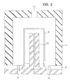
- the ground connection electrode 11 has a gas inlet 13 at upper part.
- the electrode for coating outer surface has a gas outlet 14 at lower part.
- the reactive gas and the monomer gas are introduced into the electrode through the gas inlet 13, turned to plasma, allowed to flow along the outer surface of the cylindrical vessel 9 provided with bottom, and exhausted outward from the electrode through the gas outlet 14. With this electrode, the silicon oxide film is formed on the outer surface of the cylindrical vessel 9 provided with bottom.
- the silicon oxide film was formed by the following arrangement.
- the jig 8 for sample in Fig. 1 was removed; the electrode for coating outer surface for the vessel of Fig. 2 was placed between the high-frequency electrode 3 and the ground connection electrode 2 in Fig. 1; the cylindrical ground connection electrode 2 and the ground connection electrode 11 of the electrode for coating outer surface of the vessel were connected; and the disc high-frequency electrode 3 and the high-frequency electrode 10 for coating outer surface of the vessel were connected.
- Example 4 Outside of the cylindrical vessel 9 provided with bottom of Example 4, four external high-frequency electrodes 15 were placed, as shown in Fig. 3, with equal 90 degrees angle in terms of the cylinder centers and equal distance from the outer surfaces of the cylindrical vessels. Except this, coating was performed in the same conditions as Example 4. The thickness distribution of the silicon oxide film and the water vapor permeability were determined for the barrel part of the cylindrical vessel provided with bottom. The result is shown in Table 3 together with Example 4.
- Example 4 Coating was performed in the same conditions as Example 4 except cylindrical vessel provided with bottom was axially rotated at 4 rpm. The thickness distribution of the silicon oxide film and the water vapor permeability were determined for the barrel part of the cylindrical vessel provided with bottom. The results are shown in Table 3 together with Example 4 and Comparative Example 3. Table 3 Film Thickness ( ⁇ ) Refractive Index Water Vapor permeation g/m 2 ⁇ day Observed Position 0D 45D 90D 0D 45D 90D Ex. 4 950 980 930 1.45 1.47 1.44 0.02 CEx. 3 510 1680 620 1.42 1.69 1.44 1.85 CEx. 4 940 990 950 1.55 1.60 1.58 1.05
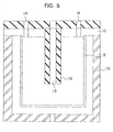
- Fig. 5 is a schematic cross-sectional drawing of an electrode for coating inner surface of a vessel used in the present invention.
- Reference numeral 9 in the drawing indicates a vessel in a cup shape, made of a cyclic olefin copolymer (hereinafter abbreviated as COC).
- Reference numeral 15 indicates the outer high-frequency electrode of which inner surface has similar shape to the inner surface of the cup vessel. The distance between the inner surface of electrode 15 and the inner surface of the vessel is constant and about 5 mm.
- Reference numeral 16 indicates the internal ground connection electrode. The outer surface of electrode 16 has similar shape to the inner surface of the cup vessel 9, and the distance between both is nearly constant and about 20 mm. Ground connection electrode 16 and high-frequency electrode 15 are placed through insulator 12.
- a cylindrical vessel, provided with bottom, made of polyethylene naphthalate (hereinafter abbreviated as PEN) was coated on the outer surface with a HMDSO polymer film and a silicon oxide film by use of the apparatus shown in Fig. 2 where the electrode for coating outer surface of the vessel was provided.
- PEN polyethylene naphthalate
Abstract
A plastic vessel of three-dimensional shape, that is coated with a silicon oxide film, wherein
said plastic is a material that has a Tg higher than the coating temperature; and
said silicon oxide film has a refractive index of 1.4 to 1.5, a thickness of 300 Å to 2000 Å and a composition of SiOx (x = 1.5 to 2.0), and is coated with a thin silicon compound polymeric film that has a refractive index of 2.0 to 2.3 and a thickness of 300 to 2000 Å.
The coating process comprises;
placing a high-frequency electrode in the surface side on which the coating is not formed, the location of the high-frequency electrode being nearly constant in a distance not more than 10 mm from the electrode surface to the vessel surface on which the coating is formed;
placing an electrode for ground connection in the surface side on which the coating is formed, the location of the ground connection electrode being nearly constant in a distance from the electrode surface to the vessel surface, which distance is greater than the distance from the high-frequency electrode surface to the vessel surface on which the coating is formed; and
adhering the silicon oxide thin firm in a uniform thickness to the surface which faces to the ground connection electrode by CVD.
Description
- The present invention relates to a three-dimensional plastic vessel that has excellent in gas-impermeability and suitable for packaging and other purposes, and relates to a process for coating a transparent silicon compound film that is excellent in gas-impermeability on a vessel made of a plastic material.
- Packaging materials are required to prevent permeation or transmission of gas for protection and preservation of the contents. Many attempts have been made to achieve this requirement. For example, efforts for providing inorganic layers such as silicon oxide or aluminum oxide, lamination of gas-impermeable resinous layers such as polyvinylidene chloride, and lamination of metallic aluminum foil have been made.
- In addition, Japanese Laid-Open Patent No. 3-183759/1991 discloses a film layer, in which an organic thin layer is formed as a coating to a plastic film by applying the synthetic resin the same as the plastic by means of vacuum deposition or sputtering, and an inorganic material is deposited in vacuum thereon to form a mixed layer of the organic and inorganic layers on which further inorganic layer is formed. Since such plastic is quite different from the inorganic layer of the coating layer and has poor affinity, the intermediate blended layer of the synthetic resin and the inorganic material is provided; however, the presence of the synthetic resin surface in the blended layer in addition to the inorganic material does not give the improvement of the fixation of the inorganic material as expected.
- Furthermore, the two-step vapor deposition of the synthetic resin and inorganic material cannot be applicable to molded products for example except sheet-form materials.
- Furthermore, the molecular weight of the synthetic resin is decreased by the vapor deposition; thereby, the vessel comprising this plastic material has poor processability.
- The present inventor previously filed patent applications for Japanese Liad-Open Patent No. 5-345385/1993 and Japanese Patent Application No. 5-224903/1993. These inventions are quite different from conventional packaging materials overcoming defects of conventional packaging materials. However, they are not satisfactory to a certain extent in formation of coated films of ultraprecise uniform thickness although coated films of uniform thickness can be formed for three-dimensional vessels. Ultraprecise uniform thickness is required for special uses such as for packaging special drugs.
- The object of the present invention is to form a film of ultraprecise thickness in which the difference of the film thickness is not more than 200 Å for example, overcomes the problem of nonuniformity in film thickness as mentioned above, and improves the gas-impermeability significantly.
- Figure 1 is a schematic drawing of a high-frequency CVD apparatus used in the present invention.
- Figure 2 is a schematic drawing of an apparatus for coating outer surface of a vessel used in the present invention.
- Figure 3 is a schematic drawing of a Comparative Example.
- Figure 4 is a drawing showing the observation position of the apparatus shown by Figure 3.
- Figure 5 is a schematic drawing of an apparatus for coating inner surface of a vessel used in the present invention.
- The present invention relates to a plastic vessel of three-dimensional shape, excellent in gas-impermeability, that is coated with a silicon oxide film, wherein the plastic can be a material that has a Tg higher than the coating temperature; and the silicon oxide film can have a refractive index of, preferably, 1.4 to 1.5, a thickness of, preferably, 300 to 2000Å, and a composition of SiOx (preferably x = 1.5 to 2.0).
- In another aspect, the invention relates to a plastic vessel of three-dimensional shape, excellent in gas-interception, that is coated with a silicon oxide film, wherein the plastic can be a material that has a Tg higher than the coating temperature; and the silicon oxide film can have, preferably, a refractive index of 1.4 to 1.5, a thickness of 300 to 2000Å and a composition of SiOx (preferably x = 1.5 to 2.0), and can be coated on a polymeric film of a silicon compound that has, preferably, a refractive index of 2.0 to 2.3 and a thickness of 50 to 500Å. Examples of plastic material can be a polyester resin such as PET or PEN, polycarbonate, or a cyclic olefin copolymer. According to the invention the silicon oxide film can be formed by the well known CVD process. Also, the silicon oxide film can be formed by the well known PVD process. Still further, the silicon oxide film can be formed by the PVD process using a mixture of silicon monoxide and silicon dioxide. Typically, the silicon oxide film can be a film that contains not less than 60% of silicon oxide compounds.
- The plastic used for the vessel or container can be a material that has a Tg higher than the coating temperature of the silicon oxide film. The process can be carried out by a method wherein a high-frequency electrode is placed in the surface side on which the coating is not formed and the location of the high-frequency electrode is nearly constant in a distance not more than 10 mm from the electrode surface to the vessel surface on which the coating is formed; an electrode for ground connection is placed in the surface side on which the coating is formed and the location of the ground connection electrode is nearly constant in a distance from the ground connection electrode surface to the vessel surface, which distance is greater than the distance from the high-frequency electrode surface to the vessel surface on which the coating is formed; and then the silicon oxide film is coated in a uniform thickness to the surface which faces to the ground connection electrode by introducing the plasma of the silicon oxide produced by CVD process in between the surface of the vessel and the ground connection electrode with a discharge gas pressure of 0.0005 to 0.05 torr. Typically, the distance from the ground connection electrode surface to the vessel surface can be nearly constant and can be 11 to 100 mm.
- The ground connection electrode can be one electrode that has the surface, facing with the coated surface of the vessel, of similar shape to the coated surface of the vessel. Also, the high-frequency electrode can be one electrode that has the surface of similar shape to the coated surface of the vessel.
- The silicon oxide film formed on the three-dimensional plastic vessel can be a refractive index of 1.4 to 1.5 and a thickness of 300 to 2000 Å.
- In another aspect, the process of the invention may include the steps wherein a high-frequency electrode is placed in the surface side on which the coating is not formed and the location of the high-frequency electrode is nearly constant in a distance, preferably, not more than 10 mm from the electrode surface to the vessel surface on which the coating is formed; an electrode for ground connection can be placed in the surface side on which the coating can be formed and the location of the ground connection electrode can be nearly constant in a distance from the ground connection electrode surface to the vessel surface, which distance is greater than the distance from the high-frequency electrode surface to the vessel surface on which the coating is formed; the polymeric film of the silicon compound can be formed on the vessel surface by introducing the plasma, which is formed by a low temperature plasma technique from an organic silicon compound comprising at least silicon, oxygen and carbon, in between the vessel surface and the ground connection electrode with a discharge gas pressure of, preferably, 3 x 10⁻³ to 3 x 10⁻² torr; and the plasma of the silicon oxide produced by CVD process can be then supplied to form a coating film of the silicon oxide onto the silicon compound film with a discharge gas pressure of, preferably, 0.0005 to 0.05 torr.
- The coated film of the polymeric silicon compound can have a refractive index of 2.0 to 2.3 and a thickness of 50 Å to 500 Å, and the coated film of the silicon oxide can have a refractive index of 1.4 to 1.5 and a thickness of 300 Å to 2000 Å.
- A feature of the present invention resides in that an external electrode can be placed outside the three-dimensional vessel; the distance from the outer surface of the vessel to the external electrode surface can be kept nearly constant; and an internal electrode can be placed inside the vessel with a nearly constant distance from the inner surface of the vessel to the electrode surface. Furthermore, it can be characteristic that the distance from the outer surface of the vessel to the external electrode surface is not more than 10 mm when the film is coated on the inner surface of vessel, and that the distance from the outer surface of vessel to the inner electrode surface can be not more than 10 mm when the thin film is coated on the outer surface of vessel. The object of keeping a constant distance between the electrode and vessel surface is to make the electric field intensity distribution constant. The distance from the high-frequency electrode to the vessel surface on which the coating is provided can be not more than 10 mm, because the longer distance can result in an undesirable sudden decrease of the gas-impermeability. The distance between the ground connection electrode and the vessel surface to be coated can be preferably longer than the distance between the vessel surface to be coated and the high-frequency electrode. When the distance between the vessel surface to be coated and the high-frequency electrode is equal to the distance between the vessel surface to be coated and the ground connection electrode, stable discharge desired is less obtainable. Under the conditions of the present invention, the discharge occurs on the side where the distance between the electrode and the vessel surface is longer. Hence, the distance between the vessel surface and the ground connection electrode is made longer so that the discharge occurs therebetween to form the coating film. The distance between the ground connection electrode and the vessel surface is preferably 11 to 100 mm, more preferably 11 to 70 mm.
- Another characteristic of the present invention is to use one ground connection electrode and one high-frequency electrode; the combination of such electrodes produces exactly constant electric field intensity distribution and makes the coated film to be formed uniform.
- A third characteristic of the present invention is to produce a plasma of silicon oxide by the CVD process with a discharge gas pressure of preferably 0.0005 to 0.05 torr. When the discharge gas pressure is not higher than 0.0005 torr, the rate of filmmaking tends to be extremely reduced and filmmaking is practically very difficult or sometimes impossible. When the gas pressure is not less than 0.05 torr, the coated film can have a problem in that the gas-impermeability is suddenly deteriorated.
- A fourth characteristic of the present invention is to use a plastic vessel, to be coated, that has a Tg higher than the coating temperature of the silicon oxide film, because deformation during the film forming should be avoided for the purpose of forming an ultraprecise film.
- These characteristics from first to fourth can be combined. Under such conditions, the plasma of silicon oxide can be introduced in between the electrode surface and the vessel wall. Since the electric field intensity distribution is constant there, the plasma concentration is constant and the silicon oxide deposits on the vessel wall in a uniform thickness for coating. In this way, a silicon oxide film with a constant thickness is formed.
- The internal and external electrodes can be one respectively. Use of plural electrodes should preferably be avoided. When a plurality of electrodes are used, a uniform film can hardly be formed even with the CVD process. The present inventor has studied the reason from various standpoints. For example, a silicon oxide was coated by the CVD process in a way shown by Fig. 3 where a plurality of electrodes were located with a constant distance to the outer surface of a vessel; however, the film thickness did not become constant as explained later in Comparative Example. Furthermore, although coating while the vessel was rotated at a constant speed to give a uniform film thickness, the coated film did not have improved gas-interception.
- The present inventor understood these phenomena as follows. The use of a plurality of electrodes intervenes the electric field intensity distribution by respective electrodes mutually causing the change of plasma concentration, by which the film thickness could not be so uniform as desired. The vessel rotation formed a mixture of films that were produced by different electric field intensities, hence a film of satisfactorily excellent gas-interception could not be formed.
- According to the present invention, the CVD process is used. As for the CVD process, high-frequency, alternating current and direct current may be used.
- The silicon oxide film formed in the present invention may have a refractive index of 1.4 to 1.5 and a thickness of 300 to 2000 Å. The film thickness not more than 300 Å does not always give a continuous film, and the coating not less than 2000 Å little improves the gas-interception and can cause undesirable film destruction by internal stress.
- The materials used for the silicon oxide plasma production by CVD process according to the present invention can include: SiH4 and NOx gas or oxygen gas; organic silicon compounds such as tetraethoxysilane (TEOS) and hexamaethyldisiloxane (HMDSO) combined with NOx gas or oxygen gas; and plasma auxiliary gas such as He or Ar gas.
- The silicon oxide film formed in this way has excellent gas-interception effect and provides excellent vessels for ordinary applications.
- The PVD process also may be used in the present invention.
- A fifth characteristic of the present invention is that either surface of the vessel can be coated by the selection of the position of the ground connection electrode, inside or outside the vessel. Plural coatings by changing the position of ground connection electrode can give coatings on both inward and outward surfaces.
- The silicon compounds used for the purpose of forming the silicon oxide film can be liquid monomers such as silane, vinylethoxysilane and phenylmethoxysilane.
- The present invention also includes a process for coating a silicon oxide film, uniform in the film thickness, on a plastic vessel of three-dimensional shape, the plastic which can be a material that has a Tg higher than the coating temperature of the silicon oxide film. A high-frequency electrode can be placed on the surface side on which the coating can be not formed and the location of the high-frequency electrode is nearly constant in a distance, preferably, not more than 10 mm from the electrode surface to the vessel surface on which the coating is formed. An electrode for ground connection can be placed in the surface side on which the coating is formed and the location of the ground connection electrode can be nearly constant in a distance from the electrode surface to the vessel surface, which distance is, preferably, greater than the distance from the high-frequency electrode surface to the vessel surface on which the coating is formed. The polymeric film of the silicon compound can be formed on the vessel surface by introducing the plasma, which is formed by a low temperature plasma technique from an organic silicon compound comprising at least silicon, oxygen and carbon, in between the vessel surface and the ground connection electrode with a discharge gas pressure of, preferably, 3 x 10⁻³ to 3 x 10⁻² torr. The plasma of the silicon oxide produced by CVD process can be then supplied to form a coating film of the silicon oxide onto the polymeric film of silicon compound film with a discharge gas pressure of, preferably, 0.0005 to 0.05 torr. The coating film may comprise two layers obtained by this process can have very high water vapor-interception effect where the permeation of water vapor is, preferably, not more than 0.1 g/m2·day, in addition to excellent gas-interception.
- When the polymeric film of silicon compound and the silicon oxide film are formed by installing the ground connection electrode and the high-frequency electrode, both films formed are uniform and the gas-interception is improved significantly.
- The reason why such special effects are brought about by the two-layer lamination in this order has not been satisfactorily explained scientifically; however, the function and effect of the present invention are realized repeatedly.
- The present inventor has understood that the gas-impermeability effect of the silicon oxide film is greatly brought about by the stable fixation of fine particles of the silicon oxide supplied to the coating substrate. That is, the supplied particles move on the plastic substrate, stabilize at the most stable position and then fixed. In this way, the presence of formed polymer film of the silicon compound containing silicon, carbon and oxygen on the plastic substrate makes the silicon oxide fine particles stabilized and fixed effectively. Thus, the particle distribution is made uniform, and intimate coating is understood to be formed by further overlaying of the silicon oxide fine particles on the stabilized silicon oxide particles.
- As for the fact that the water vapor-interception is very excellent as low as 0.1 g/m2·day or less when the first layer of polymeric film of silicon compound and the second layer of silicon oxide film are within specified range of the refractive index respectively, the present inventor has understood that these conditions result in intimate coating with higher fixation and less defect.
- The first coating layer of polymeric film of silicon compound can be the film of 50 to 500 which gives a composition of 15% or more of silicon and 20% or more of carbon, the remaining being oxygen, in the first layer. When the coating layer is thicker than specified above, the gas-impermeability can be deteriorated. The special first coating layer of polymeric film of silicon compound may be formed by, for example, turning an organic silicon compound such as hexamethyldisiloxane into plasma and polymerizing the compound on the plastic substrate. The refractive index of coated film can be made 2.0 to 2.3 by adjusting the gas pressure to 3 x 10⁻³ through 3 x 10⁻² torr in the polymerization step.
- The plasma CVD process according to the present invention is clearly special in view of the fact that the discharge gas pressure in known plasma CVD processes ranges from several torr to several tens torr although the application purposes are different.
- Examples of the organic silicone compound monomer to be used in the present invention include vinyltriethoxysilane, vinyltrimethoxysilane, tetramethoxysilane, tetraethoxysilane, phenyltrimethoxysilane, octamethylcyclotetrasiloxane, methyltrimethoxysilane, methyltriethoxysilane, 1,1,3,3-tetramethyldisiloxane and hexanemethyldisiloxane. These compounds can also be used for forming the silicon oxide film.
- The present invention also relates to a three-dimensional vessel of gas-interception which is coated with the silicon oxide film formed in this way. The vessel to be used is preferably formed from a plastic material that has a higher Tg than the coating temperature. Examples of such plastic include polyester resins such as PEN and PET, polycarbonate resins, and cyclic olefin copolymer resins. Vessels of high gas-interception can be obtained by providing a silicon oxide (SiOx: x = 1.5 - 2.0) film that has, preferably, a refractive index of 1.4 to 1.5 and a thickness of 300 to 2000 Å on the surface of three-dimensional vessels made from such plastic.
- The present invention also includes a plastic vessel which is provided with the coated polymeric film of silicon compound, as the first layer, having, preferably, a refractive index of 2.0 to 2.3 and a thickness of 50 Å to 500 Å on the surface, and is provided thereon with the coated film of silicon oxide mentioned above. The silicon oxide film can also include a film coated with a mixture of silicon monoxide and silicon dioxide by PVD process.
- Furthermore, the silicon oxide film may be comprises not less than 60% of silicon oxide and the rest of a metal compound such as TiO2, MgO, MgF2 and CuCO3. Such mixture films have a large bending strength. When the content of silicon oxide is less than 60%, the gas-interception will deteriorate.
- The present invention, will be further understood from the following examples which are illustrative.
- Fig. 1 shows a high-frequency plasma CVD apparatus that was used in the present invention for forming the polymeric film of silicon compound. This apparatus comprises: a bell-jar type vacuum chamber 1, made of stainless steel, of 60 cm diameter that has an
inlet 6 from which silane or monomer which is liquid at room temperature is introduced in gaseous condition, and has aninlet 7 for oxygen gas; high-frequency power source 5 (13.56 MHz, 1.5 kW, JEF-01B) made by JEOL Ltd. and a matching box 4; a high-frequency electrode 3 of a disc type of 13 cm diameter; a cylindricalground connection electrode 2 of 20 cm diameter and 1.5 cm height; and ajig 8 for the sample located between both electrodes. The apparatus of Fig. 1 can coat both the polymeric film of silicon compound and the silicon oxide which is the gas-interception layer. - An oil-sealed rotary vacuum pump and an oil diffusion pump were used as vacuum pumps, which were being operated during the steps of film formation.
- Hexamethyldisiloxane (hereinafter abbreviated as HMDSO) was used as the monomer which is liquid at room temperature. Oxygen gas was used as the reactive gas. These gases were introduced through separate routes, mixed in the ground connection electrode, and released into the chamber.
- The ground connection electrode and the high-frequency electrode were placed in parallel with a distance of 70 mm. A polycarbonate (hereinafter abbreviated as PC) sheet of 100 was used as the sample and placed with the aid of an insulating sample jig between the high-frequency electrode and ground connection electrode with a distance of 5 mm from the high-frequency electrode.
- Vacuum in the chamber was made to 2 - 3 x 10⁻⁵ torr (ionization vacuum gauge) by the oil-sealed rotary vacuum pump and oil diffusion pump, then oxygen gas was introduced until the vacuum became 1 x 10⁻³ torr. Thereafter, HMDSO vapor was introduced until the vacuum became 2 x 10⁻³ torr. Incident electric power of 200 W was introduced from the high-frequency power source through the matching box into the chamber, where the mixed plasma of oxygen and HMDSO was generated and kept for 10 minutes; thereby, a silicon oxide film is formed on the PC sample.
- Water vapor permeability was determined for this laminate material using a water vapor permeability meter made by Mocon. The results are shown in Table 1.
- Example 1 was repeated except the position of the PC sample placed between the high-frequency electrode and the ground connection electrode was changed to 3, 7, 9, 23, and 40 mm respectively from the high-frequency electrode. The water vapor permeation of the PC samples on which silicon oxide film was formed was determined and shown in Table 1 also.
Table 1 Distance of HFE-Substrate (mm) Water Vapor permeation g/m2·day Ex. 1 5 0.07 Ex. 2 0 0.10 3 0.09 7 0.07 9 0.10 CEx. 1 23 1.3 40 3.1 (Note): - HFE:
- Hight-frequency electrode
- CEx:
- Comarative example
-
- Example 1 was repeated except that the sample thickness was 180µ - 280µ and that a plastic sheet having a glass transition temperature (hereinafter abbreviated as Tg) of -15°C to 105°C was used. The water vapor permeation of the samples on which silicon oxide film was formed was determined and shown in Table 2. The temperature of sample surface was measured by a optical fiber type thermometer and found to be 45°C in this condition.
Table 2 Tg of Substrate (°C) Water Vapor permeation g/m2·day Ex. 3 125 0.03 115 0.04 105 0.03 97 0.04 91 0.08 67 0.1 CEx. 2 -15 0.4 - Fig. 2 is a schematic cross-sectional drawing of an electrode for coating outer surface of a vessel used in the present invention.
Reference numeral 9 in the drawing indicates a cylindrical vessel, provided with bottom, made of polyethylene terephthalate (hereinafter abbreviated as PET).Reference numeral 10 indicates the inner high-frequency electrode of which outer surface has similar shape to the outer surface of the cylindrical vessel provided with bottom. The distance between the outer surface ofelectrode 10 and the outer surface of the vessel is constant and about 5 mm. Reference numeral 11 indicates the external ground connection electrode. The inner surface of electrode 11 has similar shape to the outer surface of thecylindrical vessel 9 provided with bottom, and the distance between both is nearly constant and about 12 mm. Ground connection electrode 11 and high-frequency electrode 10 are placed throughinsulator 12. The ground connection electrode 11 has agas inlet 13 at upper part. The electrode for coating outer surface has agas outlet 14 at lower part. The reactive gas and the monomer gas are introduced into the electrode through thegas inlet 13, turned to plasma, allowed to flow along the outer surface of thecylindrical vessel 9 provided with bottom, and exhausted outward from the electrode through thegas outlet 14. With this electrode, the silicon oxide film is formed on the outer surface of thecylindrical vessel 9 provided with bottom. - By use of the apparatus shown in Fig. 1 with the electrode for coating outer surface of vessel that was equipped with the
cylindrical vessel 9 provided with bottom, a silicon oxide film was formed on the outer surface of a vessel. - The silicon oxide film was formed by the following arrangement. The
jig 8 for sample in Fig. 1 was removed; the electrode for coating outer surface for the vessel of Fig. 2 was placed between the high-frequency electrode 3 and theground connection electrode 2 in Fig. 1; the cylindricalground connection electrode 2 and the ground connection electrode 11 of the electrode for coating outer surface of the vessel were connected; and the disc high-frequency electrode 3 and the high-frequency electrode 10 for coating outer surface of the vessel were connected. - Vacuum in the chamber was made to 2 - 3 x 10⁻⁵ torr (ionization vacuum gauge) by an oil-sealed rotary vacuum pump and oil diffusion pump, then oxygen gas was introduced until the vacuum became 1 x 10⁻³ torr. Thereafter, HMDSO vapor was introduced until the vacuum became 2 x 10⁻³ torr. Incident electric power of 200 W was introduced from the high-frequency power source through the matching box into the chamber, where the mixed plasma of oxygen and HMDSO was generated and kept for 10 minutes; thereby, a silicon oxide film was formed on the outer surface of the cylindrical vessel provided with bottom.
- The thickness distribution of the silicon oxide film and the water vapor permeability were determined for the barrel part of the cylindrical vessel provided with bottom. The results are shown in Table 3.
- Outside of the
cylindrical vessel 9 provided with bottom of Example 4, four external high-frequency electrodes 15 were placed, as shown in Fig. 3, with equal 90 degrees angle in terms of the cylinder centers and equal distance from the outer surfaces of the cylindrical vessels. Except this, coating was performed in the same conditions as Example 4. The thickness distribution of the silicon oxide film and the water vapor permeability were determined for the barrel part of the cylindrical vessel provided with bottom. The result is shown in Table 3 together with Example 4. - Fig. 4 is a schematic top view of the coating apparatus of Fig. 3, in which the observed
positions 0D, 45D, and 90D are indicated. - Coating was performed in the same conditions as Example 4 except cylindrical vessel provided with bottom was axially rotated at 4 rpm. The thickness distribution of the silicon oxide film and the water vapor permeability were determined for the barrel part of the cylindrical vessel provided with bottom. The results are shown in Table 3 together with Example 4 and Comparative Example 3.
Table 3 Film Thickness (Å) Refractive Index Water Vapor permeation g/m2·day Observed Position 0D 45D 90D 0D 45D 90D Ex. 4 950 980 930 1.45 1.47 1.44 0.02 CEx. 3 510 1680 620 1.42 1.69 1.44 1.85 CEx. 4 940 990 950 1.55 1.60 1.58 1.05 - Fig. 5 is a schematic cross-sectional drawing of an electrode for coating inner surface of a vessel used in the present invention.
Reference numeral 9 in the drawing indicates a vessel in a cup shape, made of a cyclic olefin copolymer (hereinafter abbreviated as COC).Reference numeral 15 indicates the outer high-frequency electrode of which inner surface has similar shape to the inner surface of the cup vessel. The distance between the inner surface ofelectrode 15 and the inner surface of the vessel is constant and about 5 mm.Reference numeral 16 indicates the internal ground connection electrode. The outer surface ofelectrode 16 has similar shape to the inner surface of thecup vessel 9, and the distance between both is nearly constant and about 20 mm.Ground connection electrode 16 and high-frequency electrode 15 are placed throughinsulator 12. Theground connection electrode 16 has agas inlet 13 at lower part and agas outlet 14 at upper part. The reactive gas and the monomer gas are introduced into the electrode through thegas inlet 13, turned to plasma, allowed to flow along the inner surface of the cup vessel 1, and exhausted outward from the electrode through thegas outlet 14. With this electrode, the silicon oxide film is formed on the inner surface of thecup vessel 9. - By use of the apparatus shown in Fig. 1 with the electrode for coating inner surface of vessel that was equipped with the cup electrode, a silicon oxide film was formed on the inner surface of a vessel.
- The silicon oxide film was formed by the following arrangement. The
jig 8 for sample in the drawing was removed; the electrode for coating inner surface for the vessel of Fig. 5 was placed between the high-frequency electrode 3 and theground connection electrode 2 in Fig. 1; the cylindricalground connection electrode 2 and theground connection electrode 16 of the electrode for coating inner surface of the vessel were connected; and the disc high-frequency electrode 3 and the high-frequency electrode 15 for coating inner surface of the vessel were connected. Thereafter, SiH4 gas was introduced through the monomer inlet and oxygen was introduced through the oxygen gas inlet. Then, the mixed plasma of these gases was generated. A silicon oxide film was deposited on the inner surface of the cup vessel with a discharge pressure of 2 x 10⁻³ torr. The water vapor permeability of cup vessel coated with the silicon oxide film was determined and found to be 0.02 g/m2·day (40°C, 90% RH). - A cylindrical vessel, provided with bottom, made of polyethylene naphthalate (hereinafter abbreviated as PEN) was coated on the outer surface with a HMDSO polymer film and a silicon oxide film by use of the apparatus shown in Fig. 2 where the electrode for coating outer surface of the vessel was provided.
- Except for the conditions described below, the coating was performed in the same conditions as Example 4.
- Vacuum in the chamber was made to 2 - 3 x 10⁻⁵ torr (ionization vacuum gauge) by an oil-sealed rotary vacuum pump and oil diffusion pump. Thereafter, HMDSO vapor was introduced until the vacuum became 3 x 10⁻³ torr to 1 x 10⁻³ torr. Incident electric power of 400 W was introduced from the high-frequency power source into the chamber, where HMDSO plasma was generated and kept for 1 minute; thereby, a HMDSO polymer film is formed on the outer surface of the cylindrical vessel provided with bottom.
- Subsequently, the vacuum in chamber was made to 2 - 3 x 10⁻⁵ torr by the oil-sealed rotary vacuum pump and oil diffusion pump, then a silicon oxide film is formed in the same manner as Example 5 on the HMDSO polymer film. The cylindrical vessel provided with bottom coated with these films were subjected to analysis in which the refractive index and the film thickness were determined by an ellipsometer and the water vapor permeation was determined by weight method. The results are shown in Table 4.
Table 4 HMDSO HMDSO Film Water Vapor Permeation through two-layer film Conc. Coating Period Refractive Index Film Thickness Ex. 6 3 0.5 min 2.05 60 0.04 3 1.0 min 2.05 100 0.03 3 2.0 min 2.05 210 0.05 8 0.5 min 2.25 80 0.02 8 1.0 min 2.25 150 0.02 8 2.0 min 2.25 320 0.03 10 0.5 min 2.04 120 0.05 10 1.0 min 2.04 240 0.06 10 2.0 min 2.04 480 0.08 (Note):
Unit of HMDSO concentration (conc.): x 10-3 torr
Unit of film thickness: Angstrom
Unit of water vapor permeation: g/m2·day at 40°C, 90% RH - Coating was made in the same way as Example 6 on to the same cylindrical PEN vessel with bottom except that the HMDSO concentration was 1.5 x 10⁻³ torr and 20 x 10-3 torr and that the time of coating period of the HMDSO polymer film was 0.2 and 5 minutes. The refractive index and the film thickness of the HMDSO polymer film coated on the outer surface of the vessel were determined by an ellipsometer. The water vapor permeation was determined by weight method for the HMDSO laminated polymer film and silicon oxide film. The results are shown in Table 5.
Table 5 HMDSO HMDSO Film Water Vapor Permeation through two-layer film Conc. Coating Period Refractive Index Film Thickness CEx. 5 2 0.2 min 1.78 30 0.15 2 5 min 1.78 770 0.45 20 0.5 min 1.68 300 0.32 20 5 min 1.66 6000 0.47 Uncoated 0.49 (Note):
Unit of HMDSO concentration (conc.): x 10-3 torr
Unit of HMDSO polymer film thickness: Angstrom
Unit of water vapor permeation through two-layer film: g/m2·day at 40°C, 90% RH - A cylindrical vessel, provided with bottom, made of polyethylene naphthalate (hereinafter abbreviated as PEN) was coated on the outer surface with a HMDSO polymer film and a silicon oxide film by use of the apparatus shown in Fig. 2 where the electrode for coating outer surface of the vessel was provided.
- Except the cylindrical vessel provided with bottom and the conditions described below, the coating was performed in the same conditions as Example 4.
- Vacuum in the chamber was made to 2 - 3 x 10⁻⁵ torr (ionization vacuum gauge) by an oil-sealed rotary vacuum pump and oil diffusion pump, then HMDSO vapor was introduced until the vacuum became 4 x 10⁻³ torr. Incident electric power of 400 W was introduced from the high-frequency power source into the chamber, where HMDSO plasma was generated and kept for 1 minute; thereby, a HMDSO polymer film is formed on the outer surface of the cylindrical vessel provided with bottom.
- Subsequently, the vacuum in chamber was made to 2 - 3 x 10⁻⁵ torr by the oil-sealed rotary vacuum pump and oil diffusion pump, then a silicon oxide film is formed in the same manner as Example 5 on the HMDSO polymer film except that the concentration of HMDSO vapor to oxygen (HMDSO/oxygen; the ratio of vacuum in the chamber as determined by ionization vacuum gauge) was in a range from 0.5 to 2.5 and that the time of coating period of the HMDSO polymer film was 5 to 20 minutes. The cylindrical vessel provided with bottom coated with these films were subjected to analysis in which the refractive index and the film thickness were determined by an ellipsometer and the water vapor permeation was determined by weight method. The results are shown in Table 6.
Table 6 HMDSO/O2 Ratio Coating period of Si oxide Si oxide film Water vapor permeation through two-layer film Refractive Index Film Thickness Ex. 7 0.5 5.0 min 1.43 510 0.03 0.5 10.0 min 1.44 1060 0.02 0.5 20.0 min 1.44 1880 0.02 1.0 5.0 min 1.45 490 0.02 1.0 10.0 min 1.45 1080 0.02 1.0 20.0 min 1.46 2010 0.02 2.5 5.0 min 1.46 520 0.03 2.5 10.0 min 1.46 1050 0.04 2.5 20.0 min 1.46 2030 0.05 (Note):
Unit of Coating period of Si oxide: Minutes
Unit of film thickness: Angstrom
Unit of water vapor permeation through two-layer film: g/m2·day at 40°C, 90% RH - Coating of silicon oxide film was formed on the HMDSO polymer film in the same way as Example 7 except that the concentration of HMDSO vapor to oxygen (HMDSO/oxygen; the ratio of vacuum in the chamber as determined by ionization vacuum gauge) was 0.2 and 5 and that the time of coating period of the HMDSO polymer film was 2 to 25 minutes. The cylindrical vessel provided with bottom coated with these films were subjected to analysis in which the refractive index and the film thickness were determined by an ellipsometer and the water vapor permeation was determined by weight method. The results are shown in Table 7.
Table 7 HMDSO/O2 Ratio Coating period of Si oxide Si oxide film Water vapor permeation through two-layer Refractive Index Film Thickness CEx. 6 0.2 2 min 1.38 180 0.46 0.2 25 min 1.39 2350 0.14 5.0 2 min 1.59 190 0.48 5.0 25 min 1.60 2530 0.25 Uncoated 0.49 (Note):
Unit of Coating period of Si oxide: Minutes
Unit of film thickness: Angstrom
Unit of water vapor permeation through two-layer film: g/m2·day at 40°C, 90% RH - Since a silicon oxide film of uniform thickness and of a refractive index in a constant range is formed on a three-dimensional plastic vessel, a vessel of excellent gas-interception can be provided according to the present invention.
Claims (16)
- A plastic vessel of three-dimensional shape, that is coated with a silicon oxide film, whereinsaid plastic is a material that has a Tg higher than the coating temperature; andsaid silicon oxide film has a refractive index of 1.4 to 1.5, a thickness of 300 to 2000 Å, and a composition of SiOx (x = 1.5 to 2.0).
- A plastic vessel of three-dimensional shape, that is coated with a silicon oxide film, whereinsaid plastic is a material that has a Tg higher than the coating temperature; andsaid silicon oxide film has a refractive index of 1.4 to 1.5, a thickness of 300 Å to 2000 Å and a composition of SiOx (x = 1.5 to 2.0), and is coated with a thin silicon compound polymeric film that has a refractive index of 2.0 to 2.3 and a thickness of 300 to 2000 Å.
- A plastic vessel of three-dimensional shape, according to claim 1 or 2, wherein the plastic material is a polyester resin such as PET or PEN.
- A plastic vessel of three-dimensional shape, according to claim 1 or 2, wherein the plastic material is a polycarbonate.
- A plastic vessel of three-dimensional shape, according to claim 1 or 2, wherein the plastic material is a resinous copolymer of a cyclic olefin.
- A plastic vessel of three-dimensional shape, according to any one of preceding claims, wherein the silicon oxide film is formed by CVD process.
- A plastic vessel of three-dimensional shape, according to any one of claims 1 through 5, wherein the silicon oxide film is formed by PVD process.
- A plastic vessel of three-dimensional shape, according to any one of claims 1 through 5 and 7, wherein the silicon oxide film is formed from a mixture of silicon monoxide and silicon dioxide by PVD process.
- A plastic vessel of three-dimensional shape, according to any one of preceding claims, wherein the silicon oxide film is a film that contains not less than 60% of silicon oxide compounds.
- A process for coating a silicon oxide thin film, on a plastic vessel of three-dimensional shape, said plastic being a material that has a Tg higher than the coating temperature of the silicon oxide thin film, comprising:placing a high-frequency electrode in the surface side on which the coating is not formed, the location of the high- frequency electrode being nearly constant in a distance not more than 10 mm from the electrode surface to the vessel surface on which the coating is formed;placing an electrode for ground connection in the surface side on which the coating is formed, the location of the ground connection electrode being nearly constant in a distance from the electrode surface to the vessel surface, which distance is greater than the distance from the high-frequency electrode surface to the vessel surface on which the coating is formed; andadhering the silicon oxide thin film in a uniform thickness to the surface which faces to the ground connection electrode by introducing the plasma of the silicon oxide produced by CVD process in between the surface of the vessel and the ground connection electrode with a discharge gas pressure of 0.0005 to 0.05 torr.
- A process for coating a silicon oxide film, on a plastic vessel of three-dimensional shape according to claim 10, wherein the distance from the ground connection electrode surface to the vessel surface is nearly constant and is 11 to 100 mm.
- The process for coating a silicon oxide thin film, on a plastic vessel of three-dimensional shape according to claim 10 or 11, wherein the ground connection electrode is one electrode that has the surface, facing with the coated surface of the vessel, of similar shape to the coated surface of the vessel.
- The process for coating a silicon oxide film, on a plastic vessel of three-dimensional shape according to any one of claims 10 through 12, wherein the high-frequency electrode is one electrode that has the surface of similar shape to the coated surface of the vessel.
- The process for coating a silicon oxide film, on a plastic vessel of three-dimensional shape according to any one of claims 10 through 13, wherein the silicon oxide film formed on the three-dimensional plastic vessel has a refractive index of 1.4 to 1.5 and a thickness of 300 to 2000 Å.
- The process for coating a silicon oxide film, on a plastic vessel of three-dimensional shape, said plastic being a material that has a Tg higher than the coating temperature of the silicon oxide film, comprising:placing a high-frequency electrode in the surface side on which the coating is not formed, the location of the high-frequency electrode being nearly constant in a distance not more than 10 mm from the electrode surface to the vessel surface on which the coating is formed;placing an electrode for ground connection in the surface side on which the coating is formed, the location of the ground connection electrode being nearly constant in a distance from the ground connection electrode surface to the vessel surface, which distance is greater than the distance from the high-frequency electrode surface to the vessel surface on which the coating is formed;forming the polymeric film of the silicon compound on the vessel surface by introducing the plasma, which is formed by a low temperature plasma technique from an organic silicon compound comprising at least silicon, oxygen and carbon, in between the vessel surface and the ground connection electrode with a discharge gas pressure of 3 x 10⁻³ to 3 x 10⁻² torr; andthe plasma of the silicon oxide being produced by CVD process and supplying said plasma to form a coating film of the silicon oxide onto the silicon compound film with a discharge gas pressure of 0.0005 to 0.05 torr.
- The process for coating a silicon oxide film, on a plastic vessel of three-dimensional shape according to claim 15, wherein the coated film of the polymeric silicon compound has a refractive index of 2.0 to 2.3 and a thickness of 50 Å to 500 Å, and the coated film of the silicon oxide has a refractive index of 1.4 to 1.5 and a thickness of 300 Å to 2000 Å.
Applications Claiming Priority (3)
| Application Number | Priority Date | Filing Date | Title |
|---|---|---|---|
| JP340800/94 | 1994-12-26 | ||
| JP34080094A JP3022229B2 (en) | 1994-12-26 | 1994-12-26 | Method for forming silicon oxide film of uniform thickness on three-dimensional container made of plastics material |
| US08/575,618 US6254983B1 (en) | 1994-12-26 | 1995-12-20 | Process for forming silicon oxide coating on plastic material |
Publications (1)
| Publication Number | Publication Date |
|---|---|
| EP0719877A1 true EP0719877A1 (en) | 1996-07-03 |
Family
ID=26576800
Family Applications (1)
| Application Number | Title | Priority Date | Filing Date |
|---|---|---|---|
| EP95309442A Ceased EP0719877A1 (en) | 1994-12-26 | 1995-12-27 | Process for forming silicon oxide coatings |
Country Status (3)
| Country | Link |
|---|---|
| US (2) | US6254983B1 (en) |
| EP (1) | EP0719877A1 (en) |
| JP (1) | JP3022229B2 (en) |
Cited By (25)
| Publication number | Priority date | Publication date | Assignee | Title |
|---|---|---|---|---|
| EP0834597A1 (en) * | 1996-09-30 | 1998-04-08 | Becton, Dickinson and Company | Process for depositing barrier film on three-dimensional articles |
| EP0958400A1 (en) * | 1996-10-08 | 1999-11-24 | John T. Felts | Method and apparatus for plasma deposition of a thin film onto the interior surface of a container |
| US6054188A (en) * | 1999-08-02 | 2000-04-25 | Becton Dickinson And Company | Non-ideal barrier coating architecture and process for applying the same to plastic substrates |
| EP1287982A1 (en) * | 2000-05-26 | 2003-03-05 | Kureha Chemical Industry Co., Ltd. | Moistureproof multilayered film |
| DE10060418B4 (en) * | 2000-12-07 | 2004-05-06 | Alexander Freimuth | Plastic closure for beverage bottles |
| EP2249413A3 (en) * | 2002-04-01 | 2011-02-02 | Konica Corporation | Support and organic electroluminescence element comprising the support |
| US7985188B2 (en) | 2009-05-13 | 2011-07-26 | Cv Holdings Llc | Vessel, coating, inspection and processing apparatus |
| US8512796B2 (en) | 2009-05-13 | 2013-08-20 | Si02 Medical Products, Inc. | Vessel inspection apparatus and methods |
| US9272095B2 (en) | 2011-04-01 | 2016-03-01 | Sio2 Medical Products, Inc. | Vessels, contact surfaces, and coating and inspection apparatus and methods |
| US9458536B2 (en) | 2009-07-02 | 2016-10-04 | Sio2 Medical Products, Inc. | PECVD coating methods for capped syringes, cartridges and other articles |
| US9545360B2 (en) | 2009-05-13 | 2017-01-17 | Sio2 Medical Products, Inc. | Saccharide protective coating for pharmaceutical package |
| US9554968B2 (en) | 2013-03-11 | 2017-01-31 | Sio2 Medical Products, Inc. | Trilayer coated pharmaceutical packaging |
| US9664626B2 (en) | 2012-11-01 | 2017-05-30 | Sio2 Medical Products, Inc. | Coating inspection method |
| US9662450B2 (en) | 2013-03-01 | 2017-05-30 | Sio2 Medical Products, Inc. | Plasma or CVD pre-treatment for lubricated pharmaceutical package, coating process and apparatus |
| US9764093B2 (en) | 2012-11-30 | 2017-09-19 | Sio2 Medical Products, Inc. | Controlling the uniformity of PECVD deposition |
| US9863042B2 (en) | 2013-03-15 | 2018-01-09 | Sio2 Medical Products, Inc. | PECVD lubricity vessel coating, coating process and apparatus providing different power levels in two phases |
| US9878101B2 (en) | 2010-11-12 | 2018-01-30 | Sio2 Medical Products, Inc. | Cyclic olefin polymer vessels and vessel coating methods |
| US9903782B2 (en) | 2012-11-16 | 2018-02-27 | Sio2 Medical Products, Inc. | Method and apparatus for detecting rapid barrier coating integrity characteristics |
| US9937099B2 (en) | 2013-03-11 | 2018-04-10 | Sio2 Medical Products, Inc. | Trilayer coated pharmaceutical packaging with low oxygen transmission rate |
| US10189603B2 (en) | 2011-11-11 | 2019-01-29 | Sio2 Medical Products, Inc. | Passivation, pH protective or lubricity coating for pharmaceutical package, coating process and apparatus |
| US10201660B2 (en) | 2012-11-30 | 2019-02-12 | Sio2 Medical Products, Inc. | Controlling the uniformity of PECVD deposition on medical syringes, cartridges, and the like |
| US11066745B2 (en) | 2014-03-28 | 2021-07-20 | Sio2 Medical Products, Inc. | Antistatic coatings for plastic vessels |
| US11077233B2 (en) | 2015-08-18 | 2021-08-03 | Sio2 Medical Products, Inc. | Pharmaceutical and other packaging with low oxygen transmission rate |
| US11116695B2 (en) | 2011-11-11 | 2021-09-14 | Sio2 Medical Products, Inc. | Blood sample collection tube |
| US11624115B2 (en) | 2010-05-12 | 2023-04-11 | Sio2 Medical Products, Inc. | Syringe with PECVD lubrication |
Families Citing this family (12)
| Publication number | Priority date | Publication date | Assignee | Title |
|---|---|---|---|---|
| US6110544A (en) * | 1997-06-26 | 2000-08-29 | General Electric Company | Protective coating by high rate arc plasma deposition |
| JP4261680B2 (en) * | 1999-05-07 | 2009-04-30 | 株式会社クレハ | Moisture-proof multilayer film |
| US6609338B2 (en) * | 2001-05-02 | 2003-08-26 | Tenn-Tex Plastics, Inc. | Adjustable retainer clip |
| TW570876B (en) * | 2001-05-11 | 2004-01-11 | Toyo Seikan Kaisha Ltd | Silicon oxide film |
| JP4826042B2 (en) * | 2001-09-13 | 2011-11-30 | 凸版印刷株式会社 | Film forming apparatus and film forming method for cup-shaped container |
| AU2003272894A1 (en) | 2002-09-30 | 2004-04-23 | Toppan Printing Co., Ltd. | Method for forming thin film, apparatus for forming thin film, and method for monitoring thin film forming process |
| US7390535B2 (en) | 2003-07-03 | 2008-06-24 | Aeromet Technologies, Inc. | Simple chemical vapor deposition system and methods for depositing multiple-metal aluminide coatings |
| JP4711285B2 (en) * | 2004-03-26 | 2011-06-29 | 株式会社吉野工業所 | Synthetic resin container with high gas barrier properties |
| JP2005280718A (en) * | 2004-03-26 | 2005-10-13 | Yoshino Kogyosho Co Ltd | Synthetic resin container having high gas barrier property |
| JP4759263B2 (en) * | 2004-12-24 | 2011-08-31 | 株式会社ユーテック | CVD deposition system |
| JP5865617B2 (en) * | 2010-07-15 | 2016-02-17 | 太陽誘電ケミカルテクノロジー株式会社 | Plasma generation method and apparatus therefor |
| EP2785774A1 (en) * | 2011-12-02 | 2014-10-08 | SABIC Innovative Plastics IP B.V. | Coated polymer films |
Citations (6)
| Publication number | Priority date | Publication date | Assignee | Title |
|---|---|---|---|---|
| US3991234A (en) * | 1974-09-30 | 1976-11-09 | American Optical Corporation | Process for coating a lens of synthetic polymer with a durable abrasion resistant vitreous composition |
| JPH034870A (en) * | 1989-06-01 | 1991-01-10 | Nippon Steel Chem Co Ltd | Vessel for transfusion |
| FR2683230A1 (en) * | 1991-11-04 | 1993-05-07 | Siderurgie Fse Inst Rech | Process for coating a metallurgical product, product thus obtained and device for its manufacture |
| EP0566053A1 (en) * | 1992-04-14 | 1993-10-20 | Mitsubishi Chemical Corporation | Olefin resin-based articles having gas barrier properties |
| WO1994000247A1 (en) * | 1992-06-26 | 1994-01-06 | Polar Materials, Inc. | Methods and apparatus for externally treating a container with application of internal bias gas |
| US5364666A (en) * | 1993-09-23 | 1994-11-15 | Becton, Dickinson And Company | Process for barrier coating of plastic objects |
Family Cites Families (2)
| Publication number | Priority date | Publication date | Assignee | Title |
|---|---|---|---|---|
| US5641559A (en) * | 1992-10-23 | 1997-06-24 | Toyo Seikan Kaisha, Ltd. | Gas-tight laminated plastic film containing polymer of organosilicic compound |
| JP3004870B2 (en) | 1994-04-13 | 2000-01-31 | 新日本製鐵株式会社 | Continuous casting mold for casting molten steel containing zinc as an impurity |
-
1994
- 1994-12-26 JP JP34080094A patent/JP3022229B2/en not_active Expired - Fee Related
-
1995
- 1995-12-20 US US08/575,618 patent/US6254983B1/en not_active Expired - Lifetime
- 1995-12-27 EP EP95309442A patent/EP0719877A1/en not_active Ceased
-
2001
- 2001-06-14 US US09/880,135 patent/US6475622B2/en not_active Expired - Fee Related
Patent Citations (6)
| Publication number | Priority date | Publication date | Assignee | Title |
|---|---|---|---|---|
| US3991234A (en) * | 1974-09-30 | 1976-11-09 | American Optical Corporation | Process for coating a lens of synthetic polymer with a durable abrasion resistant vitreous composition |
| JPH034870A (en) * | 1989-06-01 | 1991-01-10 | Nippon Steel Chem Co Ltd | Vessel for transfusion |
| FR2683230A1 (en) * | 1991-11-04 | 1993-05-07 | Siderurgie Fse Inst Rech | Process for coating a metallurgical product, product thus obtained and device for its manufacture |
| EP0566053A1 (en) * | 1992-04-14 | 1993-10-20 | Mitsubishi Chemical Corporation | Olefin resin-based articles having gas barrier properties |
| WO1994000247A1 (en) * | 1992-06-26 | 1994-01-06 | Polar Materials, Inc. | Methods and apparatus for externally treating a container with application of internal bias gas |
| US5364666A (en) * | 1993-09-23 | 1994-11-15 | Becton, Dickinson And Company | Process for barrier coating of plastic objects |
Non-Patent Citations (2)
| Title |
|---|
| JANSEN F ET AL: "Thin film deposition on inside surfaces by plasma enhanced chemical vapor deposition", THIN SOLID FILMS, 15 NOV. 1994, SWITZERLAND, vol. 252, no. 1, ISSN 0040-6090, pages 32 - 37, XP002000775 * |
| PATENT ABSTRACTS OF JAPAN vol. 015, no. 112 (C - 0815) 18 March 1991 (1991-03-18) * |
Cited By (44)
| Publication number | Priority date | Publication date | Assignee | Title |
|---|---|---|---|---|
| EP0834597A1 (en) * | 1996-09-30 | 1998-04-08 | Becton, Dickinson and Company | Process for depositing barrier film on three-dimensional articles |
| EP0958400A1 (en) * | 1996-10-08 | 1999-11-24 | John T. Felts | Method and apparatus for plasma deposition of a thin film onto the interior surface of a container |
| EP0958400A4 (en) * | 1996-10-08 | 2002-08-14 | Nano Scale Surface Systems Inc | Method and apparatus for plasma deposition of a thin film onto the interior surface of a container |
| US6054188A (en) * | 1999-08-02 | 2000-04-25 | Becton Dickinson And Company | Non-ideal barrier coating architecture and process for applying the same to plastic substrates |
| EP1287982A1 (en) * | 2000-05-26 | 2003-03-05 | Kureha Chemical Industry Co., Ltd. | Moistureproof multilayered film |
| EP1287982A4 (en) * | 2000-05-26 | 2004-10-27 | Kureha Chemical Ind Co Ltd | Moistureproof multilayered film |
| DE10060418B4 (en) * | 2000-12-07 | 2004-05-06 | Alexander Freimuth | Plastic closure for beverage bottles |
| EP2249413A3 (en) * | 2002-04-01 | 2011-02-02 | Konica Corporation | Support and organic electroluminescence element comprising the support |
| US8834954B2 (en) | 2009-05-13 | 2014-09-16 | Sio2 Medical Products, Inc. | Vessel inspection apparatus and methods |
| US8512796B2 (en) | 2009-05-13 | 2013-08-20 | Si02 Medical Products, Inc. | Vessel inspection apparatus and methods |
| US9545360B2 (en) | 2009-05-13 | 2017-01-17 | Sio2 Medical Products, Inc. | Saccharide protective coating for pharmaceutical package |
| US9572526B2 (en) | 2009-05-13 | 2017-02-21 | Sio2 Medical Products, Inc. | Apparatus and method for transporting a vessel to and from a PECVD processing station |
| US10537273B2 (en) | 2009-05-13 | 2020-01-21 | Sio2 Medical Products, Inc. | Syringe with PECVD lubricity layer |
| US10390744B2 (en) | 2009-05-13 | 2019-08-27 | Sio2 Medical Products, Inc. | Syringe with PECVD lubricity layer, apparatus and method for transporting a vessel to and from a PECVD processing station, and double wall plastic vessel |
| US7985188B2 (en) | 2009-05-13 | 2011-07-26 | Cv Holdings Llc | Vessel, coating, inspection and processing apparatus |
| US9458536B2 (en) | 2009-07-02 | 2016-10-04 | Sio2 Medical Products, Inc. | PECVD coating methods for capped syringes, cartridges and other articles |
| US11624115B2 (en) | 2010-05-12 | 2023-04-11 | Sio2 Medical Products, Inc. | Syringe with PECVD lubrication |
| US9878101B2 (en) | 2010-11-12 | 2018-01-30 | Sio2 Medical Products, Inc. | Cyclic olefin polymer vessels and vessel coating methods |
| US11123491B2 (en) | 2010-11-12 | 2021-09-21 | Sio2 Medical Products, Inc. | Cyclic olefin polymer vessels and vessel coating methods |
| US9272095B2 (en) | 2011-04-01 | 2016-03-01 | Sio2 Medical Products, Inc. | Vessels, contact surfaces, and coating and inspection apparatus and methods |
| US10189603B2 (en) | 2011-11-11 | 2019-01-29 | Sio2 Medical Products, Inc. | Passivation, pH protective or lubricity coating for pharmaceutical package, coating process and apparatus |
| US11724860B2 (en) | 2011-11-11 | 2023-08-15 | Sio2 Medical Products, Inc. | Passivation, pH protective or lubricity coating for pharmaceutical package, coating process and apparatus |
| US11116695B2 (en) | 2011-11-11 | 2021-09-14 | Sio2 Medical Products, Inc. | Blood sample collection tube |
| US10577154B2 (en) | 2011-11-11 | 2020-03-03 | Sio2 Medical Products, Inc. | Passivation, pH protective or lubricity coating for pharmaceutical package, coating process and apparatus |
| US11148856B2 (en) | 2011-11-11 | 2021-10-19 | Sio2 Medical Products, Inc. | Passivation, pH protective or lubricity coating for pharmaceutical package, coating process and apparatus |
| US11884446B2 (en) | 2011-11-11 | 2024-01-30 | Sio2 Medical Products, Inc. | Passivation, pH protective or lubricity coating for pharmaceutical package, coating process and apparatus |
| US9664626B2 (en) | 2012-11-01 | 2017-05-30 | Sio2 Medical Products, Inc. | Coating inspection method |
| US9903782B2 (en) | 2012-11-16 | 2018-02-27 | Sio2 Medical Products, Inc. | Method and apparatus for detecting rapid barrier coating integrity characteristics |
| US9764093B2 (en) | 2012-11-30 | 2017-09-19 | Sio2 Medical Products, Inc. | Controlling the uniformity of PECVD deposition |
| US10201660B2 (en) | 2012-11-30 | 2019-02-12 | Sio2 Medical Products, Inc. | Controlling the uniformity of PECVD deposition on medical syringes, cartridges, and the like |
| US10363370B2 (en) | 2012-11-30 | 2019-07-30 | Sio2 Medical Products, Inc. | Controlling the uniformity of PECVD deposition |
| US11406765B2 (en) | 2012-11-30 | 2022-08-09 | Sio2 Medical Products, Inc. | Controlling the uniformity of PECVD deposition |
| US9662450B2 (en) | 2013-03-01 | 2017-05-30 | Sio2 Medical Products, Inc. | Plasma or CVD pre-treatment for lubricated pharmaceutical package, coating process and apparatus |
| US9937099B2 (en) | 2013-03-11 | 2018-04-10 | Sio2 Medical Products, Inc. | Trilayer coated pharmaceutical packaging with low oxygen transmission rate |
| US10912714B2 (en) | 2013-03-11 | 2021-02-09 | Sio2 Medical Products, Inc. | PECVD coated pharmaceutical packaging |
| US11298293B2 (en) | 2013-03-11 | 2022-04-12 | Sio2 Medical Products, Inc. | PECVD coated pharmaceutical packaging |
| US11344473B2 (en) | 2013-03-11 | 2022-05-31 | SiO2Medical Products, Inc. | Coated packaging |
| US10537494B2 (en) | 2013-03-11 | 2020-01-21 | Sio2 Medical Products, Inc. | Trilayer coated blood collection tube with low oxygen transmission rate |
| US10016338B2 (en) | 2013-03-11 | 2018-07-10 | Sio2 Medical Products, Inc. | Trilayer coated pharmaceutical packaging |
| US11684546B2 (en) | 2013-03-11 | 2023-06-27 | Sio2 Medical Products, Inc. | PECVD coated pharmaceutical packaging |
| US9554968B2 (en) | 2013-03-11 | 2017-01-31 | Sio2 Medical Products, Inc. | Trilayer coated pharmaceutical packaging |
| US9863042B2 (en) | 2013-03-15 | 2018-01-09 | Sio2 Medical Products, Inc. | PECVD lubricity vessel coating, coating process and apparatus providing different power levels in two phases |
| US11066745B2 (en) | 2014-03-28 | 2021-07-20 | Sio2 Medical Products, Inc. | Antistatic coatings for plastic vessels |
| US11077233B2 (en) | 2015-08-18 | 2021-08-03 | Sio2 Medical Products, Inc. | Pharmaceutical and other packaging with low oxygen transmission rate |
Also Published As
| Publication number | Publication date |
|---|---|
| US6475622B2 (en) | 2002-11-05 |
| JP3022229B2 (en) | 2000-03-15 |
| JPH08175528A (en) | 1996-07-09 |
| US6254983B1 (en) | 2001-07-03 |
| US20020058115A1 (en) | 2002-05-16 |
Similar Documents
| Publication | Publication Date | Title |
|---|---|---|
| EP0719877A1 (en) | Process for forming silicon oxide coatings | |
| JP4050800B2 (en) | Plastic container having barrier coating and method for producing the same | |
| EP0787828B1 (en) | Process for plasma processing | |
| EP0958400B1 (en) | Method and apparatus for plasma deposition of a thin film onto the interior surface of a container | |
| US5641559A (en) | Gas-tight laminated plastic film containing polymer of organosilicic compound | |
| US6001429A (en) | Apparatus and method for plasma processing | |
| CA1340053C (en) | Method of plasma enhanced silicon oxide deposition | |
| US5494712A (en) | Method of forming a plasma polymerized film | |
| EP2546388A1 (en) | Coated substrates and methods for their preparation | |
| JP4158265B2 (en) | Plastic container manufacturing method and container | |
| CN1628187A (en) | Corona-generated chemical vapor deposition on a substrate | |
| EP1799877B1 (en) | Sioc:h coated substrates and methods for their preparation | |
| JP5626308B2 (en) | Method for producing gas barrier laminate and gas barrier laminate | |
| JPH07304127A (en) | Gas barrier packaging material and production thereof | |
| US7163749B2 (en) | Process for depositing finely dispersed organic-inorganic films and articles made therefrom | |
| JP2005089859A (en) | Chemical vapor deposition film formed by plasma cvd process | |
| EP0958399A1 (en) | Barrier films having vapor coated evoh surfaces | |
| EP0154482A2 (en) | Coating process | |
| JP6834230B2 (en) | Barrier film | |
| WO2007142059A1 (en) | Plastic optical element with gas barrier film, method for manufacturing the plastic optical element, and light pickup device using the plastic optical element with gas barrier film | |
| JP3489267B2 (en) | Packaging material with excellent gas barrier properties | |
| JP6944664B2 (en) | Barrier film | |
| JPH05345831A (en) | Production of gas barrier plastic material | |
| JP4556610B2 (en) | Surface-coated plastic material | |
| JP2004169161A (en) | Transparent oxide film deposition method |
Legal Events
| Date | Code | Title | Description |
|---|---|---|---|
| PUAI | Public reference made under article 153(3) epc to a published international application that has entered the european phase |
Free format text: ORIGINAL CODE: 0009012 |
|
| AK | Designated contracting states |
Kind code of ref document: A1 Designated state(s): DE FR GB |
|
| 17P | Request for examination filed |
Effective date: 19961120 |
|
| 17Q | First examination report despatched |
Effective date: 19970620 |
|
| GRAG | Despatch of communication of intention to grant |
Free format text: ORIGINAL CODE: EPIDOS AGRA |
|
| STAA | Information on the status of an ep patent application or granted ep patent |
Free format text: STATUS: THE APPLICATION HAS BEEN REFUSED |
|
| 18R | Application refused |
Effective date: 19981016 |