EP0718979A2 - Oscillator - Google Patents
Oscillator Download PDFInfo
- Publication number
- EP0718979A2 EP0718979A2 EP95309406A EP95309406A EP0718979A2 EP 0718979 A2 EP0718979 A2 EP 0718979A2 EP 95309406 A EP95309406 A EP 95309406A EP 95309406 A EP95309406 A EP 95309406A EP 0718979 A2 EP0718979 A2 EP 0718979A2
- Authority
- EP
- European Patent Office
- Prior art keywords
- oscillator
- frequency
- signal
- output
- analog
- Prior art date
- Legal status (The legal status is an assumption and is not a legal conclusion. Google has not performed a legal analysis and makes no representation as to the accuracy of the status listed.)
- Granted
Links
- 230000010355 oscillation Effects 0.000 claims description 40
- 238000006243 chemical reaction Methods 0.000 claims description 11
- 238000001514 detection method Methods 0.000 claims description 11
- 238000001914 filtration Methods 0.000 claims 2
- 230000001360 synchronised effect Effects 0.000 claims 1
- 239000010453 quartz Substances 0.000 description 28
- VYPSYNLAJGMNEJ-UHFFFAOYSA-N silicon dioxide Inorganic materials O=[Si]=O VYPSYNLAJGMNEJ-UHFFFAOYSA-N 0.000 description 28
- 238000010586 diagram Methods 0.000 description 13
- 238000012545 processing Methods 0.000 description 10
- 230000008859 change Effects 0.000 description 9
- 238000000034 method Methods 0.000 description 9
- 230000000694 effects Effects 0.000 description 8
- 230000008901 benefit Effects 0.000 description 4
- 238000010276 construction Methods 0.000 description 4
- 239000000203 mixture Substances 0.000 description 4
- 230000004075 alteration Effects 0.000 description 3
- 230000001934 delay Effects 0.000 description 3
- 230000003111 delayed effect Effects 0.000 description 3
- 230000004048 modification Effects 0.000 description 3
- 238000012986 modification Methods 0.000 description 3
- 230000008569 process Effects 0.000 description 3
- 239000002131 composite material Substances 0.000 description 2
- 238000013016 damping Methods 0.000 description 2
- 230000003247 decreasing effect Effects 0.000 description 2
- 230000006870 function Effects 0.000 description 2
- 238000004519 manufacturing process Methods 0.000 description 2
- 230000009467 reduction Effects 0.000 description 2
- 230000000007 visual effect Effects 0.000 description 2
- 230000003044 adaptive effect Effects 0.000 description 1
- 238000004040 coloring Methods 0.000 description 1
- 239000006185 dispersion Substances 0.000 description 1
- 230000006872 improvement Effects 0.000 description 1
- 230000007257 malfunction Effects 0.000 description 1
- 239000000463 material Substances 0.000 description 1
- 230000002093 peripheral effect Effects 0.000 description 1
- 230000001603 reducing effect Effects 0.000 description 1
- 230000004044 response Effects 0.000 description 1
- 238000005070 sampling Methods 0.000 description 1
- 230000005236 sound signal Effects 0.000 description 1
- 238000001228 spectrum Methods 0.000 description 1
Images


Classifications
-
- H—ELECTRICITY
- H03—ELECTRONIC CIRCUITRY
- H03L—AUTOMATIC CONTROL, STARTING, SYNCHRONISATION, OR STABILISATION OF GENERATORS OF ELECTRONIC OSCILLATIONS OR PULSES
- H03L7/00—Automatic control of frequency or phase; Synchronisation
- H03L7/06—Automatic control of frequency or phase; Synchronisation using a reference signal applied to a frequency- or phase-locked loop
- H03L7/08—Details of the phase-locked loop
- H03L7/099—Details of the phase-locked loop concerning mainly the controlled oscillator of the loop
- H03L7/0991—Details of the phase-locked loop concerning mainly the controlled oscillator of the loop the oscillator being a digital oscillator, e.g. composed of a fixed oscillator followed by a variable frequency divider
- H03L7/0994—Details of the phase-locked loop concerning mainly the controlled oscillator of the loop the oscillator being a digital oscillator, e.g. composed of a fixed oscillator followed by a variable frequency divider comprising an accumulator
Landscapes
- Processing Of Color Television Signals (AREA)
- Stabilization Of Oscillater, Synchronisation, Frequency Synthesizers (AREA)
Abstract
Description
- The present invention relates to an oscillator which is suitable for multiple systems ready color television receivers.
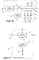
- There are three standard. i.e.. the NTSC, the PAL and the SECAM in the modulation systems of the television signal. In some areas where a plurality of systems are able to be received multiple systems ready color television receivers can be utilized. Among three systems as mentioned above, the PAL system uses different color subcarrier frequencies (fsc) in accordance with areas. For example, in South America the NTSC system, the M-PAL and the N-PAL systems are mixed. For receiving a croma signal by such TV receivers it is necessary to reproduce the color subcarrier from a transmitted burst signal. Usually, a chrominance signal processing circuit in the analog system receiver is provided a plurality of quartz oscillators (X'tals) each associated with a prescribed chrominance signal frequency and selectively uses the quartz oscillator to generates a desired color subcarrier. The system will be described in reference to FIGURE 10.
- In FIGURE 10 a burst signal input to an
input terminal 101 is supplied to one input terminal of aphase detector 102. An output of thephase detector 102 is applied to afrequency control terminal 103a of aquartz oscillator circuit 103 and to aloop filter 104.Quartz oscillators 106a to 106c which are used for an oscillation are connected to anoscillator 105 which varies the frequency by the control signal supplied to thefrequency control terminal 103a. Acontrol terminal 103b in thequartz oscillator circuit 103 connects a desired quartz oscillator among thesequartz oscillators 106a to 106c to theoscillator 105 by a control signal from outside. An output of theoscillator 105 is supplied to anoutput terminal 103c as an output of thequartz oscillator circuit 103, from here, the output is supplied to the other input of thephase detector 102. - The conventional apparatus operates to lock the phases of the input burst signal and the output of the
quartz oscillator circuit 103 with each other. When these phases are matched with each other the chrominance demodulating circuit of the system is operated to modulate a color difference signal. The PLL loop which is necessary for reproducing of the color subcarrier is called to an APC loop or an APC circuit. - When the system as described above is individually constructed for different areas there will be many types of chassises of the TV receivers so that the manufacturing process at the producer side will be complicated. So, these day there is a tendency to standardize the chassis for all of the world. Further, there was a problem that the chassis for South America has been cost-expensive since it needed three expensive quartz oscillators, as shown in FIGURE 10.
- Generally, the multi color systems ready TV means a system which is able to receive both PAL/NTSC systems. In this case of TV still needs two quartz oscillators. While the SECAM system adapts a FM modulation system different from other systems, so that it takes different chrominance demodulation processing. So, it has a processing circuit in addition to the those for the PAL and NTSC systems, and it does not need the oscillation circuit. Accordingly, the oscillation circuit needs to accommodate four frequencies of a BG-PAL system (4.43 MHz), an M-PAL system (3.575 MHz), an N-PAL system (3.582 MHz) and the NTSC system (3.579 MHz).
- In such an environment as described above, these day a system accommodating not an analog technique as shown in FIGURE 10 but a digital technique as shown in FIGURE 11 is introduced. The digital system is mentioned in "direct processing digital synthesizer" in "Design and Application of Oscillators", pp. 305-329 issued by CQ Publishing Co. Ltd. Here, the digital system will be called as a "digital oscillator circuit" and incorporated herein in place of the
quartz oscillator circuit 103 in the analog TV receiver, as shown in FIGURE 10. - In FIGURE 11, a clock signal fCFK generated in a
clock generator 112 is supplied to adigital oscillator 111 as a master clock. And, the oscillation frequency is varied by a data supplied from a frequency controldata input terminal 113 of thedigital oscillator 111. As adigital oscillator 114, which will be described in detail later, can accurately change its oscillation frequency to any given value by changing data, it can generate all of the four color subcarrier frequencies fsc. The system, as shown in FIGURE 11, needs only onequartz oscillator 115 for the master oscillation, so that it can achieve the standardization and the cost reduction at a same time. - Peripheral parts of the APC in the chrominance signal processing part will be explained in reference to FIGURE 12. In FIGURE 12 a digital oscillator system is constructed on a chassis accommodating a digital circuit. The same elements as these shown in FIGURE 11 are assigned with the same reference numerals.
- Only the burst signal is extracted from the analog composite video signals and carried out an A/D conversion by an A/D convertor (not shown). A
digital phase detector 121 compares the phases of the digitized burst signal supplied to aninput terminal 122 with the output of thedigital oscillator 111 lead to anoutput terminal 123. The comparison result data ΔSA is supplied to afrequency control terminal 113 of thedigital oscillator 111 through aloop filter 124. Besides the comparison result data ΔSA, a control signal for changing color subcarrier frequencies fsc in suited for the prescribed system is supplied to aninitial data generator 126 from acontrol terminal 125. Theinitial data generator 126 generates initial data ΔSO for obtaining each oscillation frequency fsc and applies each color subcarrier frequency fsc to anadder 127. The initial data ΔSO and the comparison result data ΔSA are added in theadder 127 and then the resulted sum data ΔS from theadder 127 is input to adata accumulator 128. Thedata accumulator 128 outputs an oscillation data under the control of the master clock fCLK from theclock generator 115. - Before explaining about the APC operation, the operation of the
data accumulator 128 will be explained in reference to FIGURE 13. Thedata accumulator 128 comprises anaccumulator 131 and awaveform converter 132, as mentioned in the above-referenced document. Theaccumulator 131, which comprises a full adder and a latch, adds the recent output sum data and the sum data ΔS at every one clock of the master clock fCLK. In such a construction as described above, the output of theaccumulator 131 will be increased by the amount of the sum data ΔS at every the every master clock fCLK, and it will cause an overflow of data in the end. Then, it looks that the data drops toward 0 and presents a sawtooth waveform. Accordingly, if the master clock fCLD is constant and once the bit length of the adder has been fixed, the interval causing the overflow is varied by changing the sum data ΔS. Regarding the interval as an oscillation frequency, the oscillating frequency can be controlled by the sum data ΔS. Here, the output data of theaccumulator 131 has a sawtooth waveform, though generally it is desirable to provide a sinusoidal waveform signal to the APC circuit. This is because that the sawtooth wave contains a large amount of noise to make difficult the normal phase detecting operation of the APC. So, the sawtooth waveform data sequence is replaced by the sinusoidal waveform signal in the waveform converter. - Many of embodiments of the waveform converter used in this case are realized by sinusoidal waveform data storing ROMs, as mentioned in document. In the sinusoidal waveform data storing ROM the sinusoidal waveform data is stored by associating addresses in advance. Then the sinusoidal waveform data are read by assuming the sawtooth waveform data sequence as the addresses. According to the assumption, the sawtooth waveform data sequence is changed to the sinusoidal waveform data sequence so that it can output the signal suitable for the APC. Since the phase detector multiplies the burst signal and the oscillating signal generated in the digital generator, it has basically no problem when the phase of the oscillating signal is fixed. It is the most stable to get a duty 50 % signal in this mean the sinusoidal waveform data storing ROM is mentioned here. If only the basic operation is discussed the waveform need not to changed to the sinusoidal waveform, it can be changed to a triangular wave or short from wave. Here, the waveform conversion is not specified to the sinusoidal waveform data storing ROM to take it in the wide sense.
- The oscillation frequency control of the
digital oscillator 114 is realized by changing the sum data ΔS. However, since the APC circuit operate to lead the frequency in it the data for establishing the initial frequency and the data for changing the frequency little are treated separately. The initial frequency, that is the free run frequency is established by the initial data ΔSO and the data for changing the frequency is established by the comparison result data ΔSA. Thephase detector 121 is a phase comparator and multiplies the burst signal and the output signal of thedata accumulator 128. Only the data at a low frequency is extracted through aloop filter circuit 124 by the multiplied result. Since the extracted data varies a little the oscillation frequency of thedigital oscillator 114 is made equal to the burst frequency to finally synchronize with the burst frequency. Thus, the color subcarrier frequency fsc equal to the burst frequency is reproduced. - In the system using the
digital oscillator 114 as described above, since the data frequency oscillated in thedigital oscillator 114 is defined by the initial data ΔS, i.e., the digital data, the bit length needed in thedata accumulator 128 for obtaining a required resolution becomes extremely large and it causes a problem of a large scale circuit, that is a high cost. Since the frequency is controlled by the digital data the oscillation frequency takes only the discrete value and it does not accord to the input burst frequency accurately. Accordingly, the output data of thephase detector 121 causes a frequency jump corresponding to at least one bit of data and change of the oscillation frequency of thedigital oscillator 114 each phase detection (one time each one horizontal line). Since the change of the oscillation frequency leads the phase change of the color subcarrier signal fsc and also the change of the demodulated color phase. To check the phase difference the extent that it is not see by human eyes when it is received, it is necessary to check the effect of the frequency jump corresponding to one bit of data as small as possible. It is assumed that the 0.4 degree is a detection limit by the end of one line video signal since the burst is detected. It is about 30 Hz in the frequency of the color subcarrier fsc. - This is the bit resolution of the
digital oscillator 114. If the bit length has an N bit size it is necessary to set the master clock fCLD/2N below 30 Hz. When the master clock fCLD is assumed as 16 MHz N will be 19. When a margin from a detection limit is considered N will be around 22 to 24. Whether theaccumulator 131 having so many bits can be added by the master clock fCLK at once will be rely on the speed of theaccumulator 131. - However, since it is difficult to process the addition at once in the present device technique, the addition is usually performed by being divided into an upper bit part and a lower bit part so that the added data in the lower bit part is carried to the upper bit part by the next clock and added. The added data in the lower bit part is delayed by the latch so as to align the timings of all bit of the adding output timing. The faster the clock becomes, the smaller the bit have to be defined. Further, the faster the clock becomes, the more the added output in the lower bit part delays by the latch and the more the number of stages of the latch will be, so that the stages of the latches will be increased aside from the main body, i.e., the
adder 127. - Further, if the
phase detector 121 is configured by a digital circuit, since the operation is operated by a multiplication process the output will be delayed by the step of the clock frequency. In addition, the APC information is supplied to the digital oscillator delayed for some clocks by the output delay for taking a timing of the comparison result data ΔSA and the initial data ΔSO in theadder 127, it seriously effects the APC pull-in time. In the case of the analog APC in FIGURE 10 since the multiplication processing is performed in real time it does not cause to delay the clock. In the cases of FIGURES 10 and 11, since the loop filter is located after the phase detector only low frequency components of the detected APC pass through the filter. Here, the delay time also presents but both the delays in the analog system and the digital system become equal, so it can be neglected. The delay of the signal over the phase detection to the digital oscillator results to cause the APC pull-in time longer. - Empirically, in the case of the analog APC system the APC pull-in operation completes within four fields, however in the case of the digital system in FIGURE 12 it extends over about eight fields. When the color subcarrier signal fsc to be received is limited to one like receivers for Japan the time difference between four fields and eight fields, in other wards, the coloring time required at a channel changing operation is not a big problem. However, in the case of the multi color systems ready receiver it will be a big problem. That is, as shown in FIGURE 10 when there is a difference between the frequency oscillated from the
oscillator 105 and the burst frequency it repeats the change of the quartz oscillators such that it changes the quartz oscillators after a time and performs the APC detection again with other quartz oscillator. Since the quartz oscillators are not changed in APC pull-in time the time for changing the quartz oscillators will take a time the same or longer than the quartz oscillator changing time. - For example, if the cycle equals to eight fields, the changing operation of three quartz oscillators takes 31 fields long in maximum until the completion of the APC pull-in operation. It corresponds to 0.5 seconds, so that it makes viewers to feel nervous. In the case of the analog circuit similarly to the digital circuit when the cycle equals to four fields it takes 15 fields in maximum and it corresponds to 0.25 seconds. The difference of the 0.25 seconds has a great effect on visual sense since the difference is discriminated by a human. In other words, a human eye sharply responds the time differences. Practically, since the quartz oscillator changing cycle takes longer than the frequency pull-in time the absolute time will be expanded. In other words, the degree of feeling the time dull will be increased.
- As described above, the conventional oscillator using the full digital APC system configured by direct composition system digital synthesizers has drawbacks such as a slow APC pull-in operation, a low precision, a large circuit scale (23 bits) or a cost-up, although it needs only one quartz oscillator in the multi-standards ready television receiving system.
- The present invention seeks to provide an oscillator which is able to be used for an APC (PLL) circuit etc which circuit scale is small, and have a short APC pull-in time.
- According to the present invention, there is provided an oscillator, comprising:
- a frequency-controllable clock generator; and
- a digital oscillator responsive to a clock generated by the clock generator for oscillating a data sequence at a period in proportion to the clock and also discretely controllable in accordance with a frequency switching signal.
- According to one embodiment of the present invention the oscillator includes a clock generator where the frequency changes in an analog operation by an impressed voltage or current of an analog controls the bit length of the accumulated data oscillator takes an error of the initial oscillation frequency as large as possible within an acceptable range and eliminates the adder for adding the comparison result data ΔSA and the initial data ΔSO. Further, the output of the phase detector is took out by the analog system and impressed to the clock generator, so that the object as described above is achieved.
- According to the arrangement as mentioned above, since the bit length is shortened in the accumulated data generator the accumulator scale itself is reduced. Further, since the steps for dividing the additional bit is reduced the steps of the latch for delaying the added result is also reduced. Since it does not have the adder for adding the comparison result data ΔSA and the initial data ΔSO the element reduction effect in the digital oscillator can be increased, since the master clock fCLK is controlled from the phase detector using an analog operation the oscillation frequency in the digital oscillator which is conventionally dispersed so far can be took to analog and the limitation of the frequency resolution in the digital oscillator can be removed.
- Additional objects and advantages of the present invention will be apparent to persons skilled in the art from a study of the following description and the accompanying drawings, which are hereby incorporated in and constitute a part of this specification.
- For a better understandings of the present invention and many of the attendant advantages thereof, reference will now be made by way of example to the accompanying drawings, wherein:
- FIGURE 1 is a block diagram for explaining one embodiment of the present invention;
- FIGURE 2 is a block diagram for explaining an application of the present invention using FIGURE 1;
- FIGURE 3 is a block diagram for explaining a concrete example of the analog converter in FIGURE 2;
- FIGURE 4 is a block diagram for explaining other application of the present invention using FIGURE 1;
- FIGURE 5 is a block diagram for explaining other different application of the present invention which adds the phase controller to the analog phase detector;
- FIGURE 6 is a block diagram for explaining more concrete example which combines the system of the television standard discrimination with the system in FIGURE 5;
- FIGURE 7 is a block diagram for explaining a slight adjustment of the oscillation frequency of the present invention;
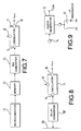
- FIGURE 8 is a block diagram for explaining other slight adjustment of the oscillation frequency of the present invention;
- FIGURE 9 is a block diagram for showing external converting example of the clock generator of the present invention;
- FIGURE 10 is a block diagram showing a conventional APC circuit;
- FIGURE 11 is a block diagram showing a conventional digital oscillator;
- FIGURE 12 is a block diagram for explaining a digital APC circuit using FIGURE 11; and
- FIGURE 13 is a block diagram for explaining an accumulated data generator in FIGURE 12.
- Embodiments of the present invention will be explained hereinafter in reference to the attached drawings, FIGURES 1-9.
- FIGURE 1 shows a system illustrating one embodiment of the present invention. In FIGURE 1, the
reference numeral 11 denotes a digital oscillator. In the digital oscillator 11 a master clock fCLK is generated by connecting onequartz oscillator 13 to an analogsystem clock generator 12. An analog control signal is input to theclock generator 12 through afrequency control terminal 14. The master clock fCLK is supplied to adigital oscillator 15, from which the color subcarrier signal fsc is then introduced to anoutput terminal 16. A control signal for changing the oscillating color subcarrier signal fsc associated with a particular television system is input to thedigital oscillator 15 through acontrol terminal 17. - The detail explanation will be described after. The
digital oscillator 11 does not have the input of the comparison result data ΔSA in FIGURE 12, so, it also does not have anadder 127 in FIGURE 12. Since the master clock fCLK changes in analog operations so as to obtain the desirable frequency it will be needless to consider the bit resolution in thedigital oscillator 11. Besides, since the frequency jump corresponding to one bit of data does not occur by the complete phase synchronization it is also needless to discuss about the color phase difference detection limit at the one line ending time. - FIGURE 2 shows an example of the case that the system in FIGURE 1 is applied as the APC circuit of the TV receiver, the embodiment is explained hereinafter by using this FIGURE 2. The same component as those shown in FIGURE 1 are assigned with the same marks.
- A burst signal divined from a composite video signal is applied to an
input terminal 22 of ananalog phase detector 21, here, the output of thedigital oscillator 11 is phase-compared with the analog conversion signal via ananalog converter 23. An output signal which is extracted its low frequency band by aloop filter 24 is connected to afrequency control terminal 14 of aclock generator 12. Theclock generator 12 changes the oscillation frequency by a frequency control signal. The oscillation signal obtained from theclock generator 12 is input to thedata accumulator 15a composing adigital oscillator 15, as a master clock fCLK. On the other hand, a signal for changing the frequency of the color subcarrier signal fsc is input to aninitial data generator 15b composing thedigital oscillator 15 from a changingterminal 17. The initial data which is for defining the initial oscillation frequency of the color subcarrier signal fsc changes the initial data ΔSO which is equal to a given sum data ΔS of the according to the changing signal. Since the comparison result data ΔSA is not in the accumulated data of the accumulateddata generator 15a the initial data ΔSO is equal to the given sum data ΔS. As explained in the conventional example, in the accumulateddata generator 15a the sum data ΔS is added each master clock fCLK. Since it rises an overflow a sawtooth waveform data sequence is obtained apparently, by operating the waveform (sinusoidal waveform) converting to the data sequence a data sequence output having a least distortion is obtained. - An analog output signal which is obtained from the burst signal and the output of the
digital oscillator 15 via ananalog converter 23 is phase-compared in aphase detector 21, and the comparison result is obtained by the analog. The signal is passed through theloop filter 24 to extract only the low component and supplied to theclock generator 12 as it is analog. In theclock generator 12 the frequency changes very little by the signal, as a result it changes the output frequency of thedigital oscillator 15. At the end thephase detector 21 drives the oscillation frequency of thedigital oscillator 15 and make it to phase-synchronize with the burst signal wholly. The sum data ΔS only do only controlling the initial oscillation frequency. Since the phase detecting controlling is operated to the master clock fCLK the controlling parameter is divided into two apparently, it is not necessary to add the APC controlling information on the sum data ΔS. Generally speaking, thefsc changing terminal 17 is provided for a coarse adjustment while thefrequency control terminal 14 is operated for a fine adjustment. - In the conventional system shown in FIGURE 10 since the frequency band of the
quartz oscillator circuit 103 is about from ±500 to ±700 Hz compared with that of the color subcarrier signal fsc, if theclock generator 12 in FIGURE 2 has the same ratio that is, for instance, the master clock fCLK is 16 MHz which is four times as much as the frequency of the color subcarrier fsc it can have the frequency band about from ±2 to ±3 KHz. The setup is enough to be corresponded by the analog circuit. Since the master clock is varied in thedigital oscillator 15 the error from the frequency of the color subcarrier signal fsc of the initial oscillator by ΔS can be large. If anything, it may be an initial oscillation frequency error extent of the conventional oscillator in FIGURE 9, and it is about from ±5 0 to 100 Hz. If the bit length of the accumulated data generator has an M bit size (M is an integer) to a certain master clock fCLK the oscillation frequency fosc of thedigital oscillator 15 can be expressed by the following Equation;
- The initial data ΔSO in the conventional system, as shown in FIGURE 12, will be that M = 22 and the value of the sum data ΔS = 1162247 when it is calculated from the equation (1) in the case of the BG-PAL system. It need almost the same bit length as the accumulating addition of the accumulated
data generator 128. However, in this embodiment, the adder is not necessary so, it can get almost the half of the scale reducing effect as a whole system f thedigital oscillator 11. - Since the output of the
analog phase detector 21 does not have a element of the clock delay, it can be got at real-time. Further, since it also does not have the clock delay factor which was needed for synchronizing the timing of the comparison result data ΔSA and the initial data ΔSO in theadder 127 in the conventional FIGURE 12 the same pull-in time as the APC in FIGURE 10 can be obtained. Accordingly the operation which is took eight fields in FIGURE 11 can be done with four fields in this embodiment,that is, the improvement effect on the visual sense is extremely great. - Here, the construction of the accumulated
data generator 15a in FIGURE 2 is the same as an accumulateddata generator 128 in FIGURE 12 and the construction example is the same as FIGURE 13. So, its detail explanation will be omitted, but since the bit length composing the circuit is different each other it can not be regarded in the same light as the constructing example in FIGURE 13. - Next, the embodiment of the
analog converter 23 in FIGURE 2 is explained by using FIGURE 3. It is a circuit which inputs the data sequence from the accumulateddata generator 15a and converts the data into the analog signal. The data sequence from the accumulateddata generator 15a is took into theinput terminal 16. The input data sequence is converted into the analog signal in a D/A converter 23a. However, since the output signal is still performed a sampling it just converted into a voltage signal. Accordingly, it leaves a lot of spurious components containing an alias behind, so it has to remove them. The spurious components are removed in aspurious rejection circuit 23b. An analog color subcarrier fsc is output to anoutput terminal 31 from thespurious rejection circuit 23b. The conventional circuit shown in FIGURE 13 does not have theanalog converter 23, but the analog output is necessary to take anoscillator 114 in FIGURE 11 into the analog system as a matter of course, and thus the analog converter is necessary as well. - FIGURE 4 shows another system of the APC circuit according to the present invention, which is incorporated with a digital phase detector without the use of the analog phase detector. A burst signal of the digital data which is converted in the A/D converter (not shown) is input through an
input terminal 41 to one input of adigital phase detector 42, a digital output from theoutput terminal 16 of anoscillator 11 is applied to the other input of thedigital phase detector 42 to be phase-detected. The detected output data is supplied to ananalog converter 44 via aloop filter 43. The analog conversion signal is supplied to a frequencycontrol input terminal 14 of theoscillator 11 to control the oscillation frequency of theclock generator 12. According to the above configuration, the clock is controlled in analog operations. Thus it is possible to reduce the bit length of theoscillator 11 and thus decreasing the cost of theoscillator 11. - However, in the case of FIGURE 4 since the phase-detection output represents a digital signal the frequency jump corresponding to one bit of data as explained in reference to FIGURE 12 occurs. The degree of the frequency jump is depend on the bit size of the analog conversion or phase-detection output. But, those matters can be improved changing the positional order of the
loop filter 43 and theanalog conversion circuit 44 by configuring in analog operations theloop filter 43 or properly adjusting the characteristics of theloop filter 43. At least, since delays such as those caused in theadder 127 in the conventional system as shown in FIGURE 12 do not occur in the system, as shown in FIGURE 4, the APC pull-in time is improved in compared to that in the conventional system of FIGURE 12. - Thus, the APC circuits according to the present invention do not lower the essential effect of the circuits though there is a slight difference in the digital or analog configuration of the phase detector.
- Referring now to FIGURE 5, still another system of the APC circuit according to the present invention will be explained. The system shown in FIGURE 5 is a modification in which a
phase controller 51 is added for processing the control signal to theanalog phase detector 21, as shown in FIGURE 2. In a specific application, it is desired to make the phase of the signal supplied to the phase detector different from the phase of the signal used in other circuits. In this case, thephase controller 51 is located to receive the analog conversion signal output from theanalog converter 23. An output of thephase controller 51 is fed back to thephase detector 21. Thephase controller 51 thus outputs another phase-controlled signal as the color subcarrier signal fsc. Here, when a phase controller such as thephase controller 51 is used in the system as shown in FIGURE 4 the phase controller can be inserted between theoutput terminal 16 of theoscillator 11 and thephase detector 42. - Referring now to FIGURE 6, the system as shown in FIGURE 5 in cooperated with the television standard discriminating system will be described. Further, the function of the
fsc changing terminal 17 in television receivers will be also explained. Accordingly, In FIGURE 6 the analog phase detector is illustrated based the circuit configuration of analog phase detectors. - In FIGURE 6, the output of the
oscillator 11 is converted into analog signals in theanalog converter 23 and then input to thephase controller 51. One output of thephase controller 51 is fed back to theanalog phase detector 21. A televisionstandard discrimination system 61 is provided for receiving the output signal from thephase controller 51, the input burst signal on theinput terminal 22 and a clock signal CK through aclock input terminal 62. The output of thediscrimination system 61, i.e., an fsc changing signal is fed back to thecontrol terminal 17 of theoscillator 11. The televisionstandard discrimination system 61 is provided with anNTSC killer circuit 63 and aPAL killer circuit 64 which receive the burst signal. Thephase detector 51 provides theNTSC killer circuit 63 and thePAL killer circuit 64 with respective suitably phase-controlled color subcarrier signals fsc. The outputs of thekiller circuits standard discrimination circuit 65 for discriminating the standard of the presently received signal. - The
NTSC killer circuit 63 discriminates whether the presently received signal is of the NTSC signal or not by processing the phase-controlled color subcarrier fsc and the burst signal. ThePAL killer circuit 64 discriminates in the same manner as theNTSC killer circuit 63. However, since the burst signal at the PAL system has different phases at line by line thePAL killer circuit 64 provides the color subcarrier signals fsc suitably phase-controlled in synchronism with the phase change of the burst signal. Since the phase control as mentioned above is needed for the processing of the color subcarrier signal fsc of the TV receiver the phase controller is located between theoscillator 11 and thephase detector 21. Besides, such a phase control is also needed for the color subcarrier signal fsc supplied to demodulators. The clock signal CK input to the televisionstandard discrimination circuit 65 is of a four field cycle clock signal, thus the televisionstandard discrimination circuit 65 generates the fsc changing signal based on the unit of the four field cycle. For instance, when a signal is of neither the NTSC system nor the PAL system the frequency of the color subcarrier signal fsc is changed every four fields. In theinitial data generator 15b the value of the sum data ΔS is changed based on the signal changing every four field of the color subcarrier signal fsc. Thus, the television standard of the presently received chrominance signal is discriminated. - Here, if the PAL standard signal is received the
PAL killer circuit 64 outputs a signal corresponding to the PAL standard signal. The televisionstandard discrimination circuit 65 discriminates the output signal of thePAL killer circuit 64 as a signal of the PAL system in referring the output of theNTSC killer circuit 63 or the color subcarrier signal fsc. At the time, the fsc changing signal is deactivated and the current frequency of the color subcarrier signal fsc is maintained. Further, a PAL demodulating circuit (not shown) is activated for reproducing a PAL demodulating color difference signal. Similar operations are also carried out in the case of receiving the NTSC standard signal. - Since the SECAM standard system carried out processings different from the PAL and the NTSC standard system, the operation for receiving the SECAM standard signal is basically not related to the oscillation of the color subcarrier signal fsc. However, if the
fsc oscillator 11 changes the oscillation frequency at the SECAM receiving time the chrominance signal displayed on a screen is affected by a leakage signal of the color subcarrier fsc. So. in the SECAM receiving time the color subcarrier signal fsc is usually fixed with that of the PAL or the NTSC system. Thus, it is needed to monitor killer information of the SECAM system at the televisionstandard discrimination circuit 65. When the receiver is fully adapted to receive the SECAM system the killer information of theSECAM killer circuit 66 is input to the televisionstandard discrimination circuit 65 and the comprehensive television standard discrimination is carried out. Even if such full multi standards ready color television receiver adapted for all standards including the SECAM standard is considered, the presently received standards is sure to be automatically discriminated by cyclically performing the change of the color subcarrier signal fsc. - In the case of the television receiver for South America the sum data ΔS can be prepared for the NTSC system and M-PAL and N-PAL system, and in case of the television receiver for Europe or Asia, BG or others-PAL and NTSC can be changed.
- On the other hand, in the case of the PAL system, its color subcarrier is interleaved between the horizontal frequencies by means of so-called 1/4 line offset techniques. Since the burst signal is phase-controlled to 90 degree every line apparent frequencies are not unified. Since sideband components caused by the operation are combined on a frequency axis if the pull-in frequency range of the color subcarrier signal fsc at the receiving side is wide the sideband components cause a malfunction of fault-locking to the sideband components. So, for oscillating the color subcarrier signal fsc a device such as a quartz oscillator which has a stable reference frequency, a high degree of Q and around 10-6 (i.e. PPM) order in errors of the frequency variable limits and the initial oscillation frequency could be used.
- Actually, in the case of the conventional
quartz oscillator circuit 103 in FIGURE 10, by means of that the damping resistance on the terminal provided for connecting to the PAL system quartz oscillators is lowered to decrease the Q of the circuit, and the frequency band is made so wide that the variable limits is checked not to expand to the frequency causing the fault-locking. Hereinafter some measures applied in the present invention will be described in detail. - In the digital oscillator of the present invention, the oscillation frequency of the
clock generator 12 is fixed, i.e., unchanged even if it generates either frequency needed for the color subcarrier signals fsc of the above-mentioned four standards. However, since the ΔS of aninitial data generator 15b is controlled by atelevision standard discriminator 65 the oscillated frequency can be discriminated between the PAL and the others. Accordingly, the frequency band of theoscillator 11 in the case of the PAL standard is narrower than the that of the other standards, so that it is able to carried out an adaptive control. Generally, the frequency band of theoscillator 11 is defined by not only a damping resistance but also a vector composition ratio. - About the configuration of the
oscillator 11, see the Japanese patent application: Tokkai-Hei 2-200002 in the title of "Voltage Controlled Oscillator". By making the vector composition ratio small the frequency variable limits can be controlled from outside. So, when the signal is oscillated with PAL frequency the vector composition ratio may be controlled or changed to become small. Of course, when the signal is oscillated with PAL frequency a specific variable limits is set up and when it is oscillated with the other color subcarrier signals fsc the variable limits can be widen. - The embodiment mentioned above explains about the case of that the system in FIGURE 1 is input to the PLL loop. The case of that the system is not input to the PLL loop will explained hereinafter.
- In some applications the oscillation frequency of the oscillator can be changed in a step-wise manner and so that a frequency-locking is not required. For instance, there is an application to an SIF (sound intermediate frequency) handling in the multi-standards ready color television receiver. There are four television standards of the SIF handling in television signals. In Japan the 4.5 Mhz is used for the SIF, while globally there are also used 5.5 MHz, 6.0 MHz and 6.5 MHz for the SIF. When these SIF signals are received in one television receiver these are frequency-converted to a single IF so that it is able to be processed by only one audio signal detection circuit. There are many ways in the frequency arrangement. For instance, if the second IF next to the first frequency conversion is set to 500 KHz the television receiver is required to accommodate four local oscillation frequencies of 4.0 MHz, 5.0 MHz, 5.5 MHz and 6.0 MHZ for ion of the 4.5 MHz SIF, the 5.5 MHz SIF, the 6.0 MHz SIF and the 6.5 MHz SIF. The present invention is suitable for applying to such an SIF local oscillator. As the second IF it will be enough to have a tracking efficiency of 0.1% order for converting down the frequency of the received signal to about 500 KHz. Generally, a reference oscillator is provided for the usage. Then some of integer-times frequencies are produced from the reference frequency by using a frequency synthesizer and thus the produced frequencies are used as respective local oscillation signals. In this case, many frequency dividers and a loop filter are required since the frequency synthesizer is itself arranged in a PLL configuration.
- On the other hand, the oscillator according to the present invention has an advantage of that it can generate arbitrary frequencies from the reference signal and it does not require to use such a loop filter. In other words, in the conventional system the PLL technique is used for overcoming the unstableness of oscillation frequency due to dispersion of time constant obtained IC configuration. On the other hand, the present invention system can provide a good precision of the reference frequency without the use of the PLL technique. Further, since a spectrum of the signal obtained from the
digital oscillator 11 has the same precision as theclock generator 12 for the reference signal and also it provides an extremely pure color presentation with less spurious. Although the present invention does not need the APC (PLL) loop, the initial oscillation error in theclock generator 12 or the initial oscillation data error caused by controlling the bit length of the accumulateddata generator 15a may cause a slight aberration in the tracking frequency. Referring now to FIGURES 7 and 8, a compensation of the aberration will be is described. The choice of the receptions with which frequency among the above-mentioned four television standard SIFs will be determined by an indication from a microcomputer. So, if proper compensations corresponding to these four television standards are done it is possible to cancel the error. - In FIGURE 7, compensation data are provided from a
microcomputer 71 to amemory 72. An output of thememory 72 is supplied to a D/A converter 73. An analog output from the D/A converter 73 is supplied to afrequency control terminal 14 of theoscillator 11. In this case, the clock frequency is controlled by an analog voltage or current signal converted from the compensation data from themicrocomputer 71. Thememory 72 can be of either a RAM or a ROM. The compensation data can be prepared by adjusting once and then applied to the microcomputer every time. Or the compensation data can be stored in a ROM in advance and then are selectively read from the ROM in response to a changing signal of the four standard SIFs. Further, when the SIF frequency changing using the changingterminal 17 is performed with a sufficient precision a control data from themicrocomputer 71 can be used for adjustment of the master clock fCLK. Thus, it can output different frequencies with a high precision and a high purity. In manufacturing lines since the data is managed by microcomputers the adjustment process does not need skills. So it is extremely good. - When it is unable to adjust with the aid of microcomputers the adjustment can be manually adjusted as shown in FIGURE 8. In this case, the aberration to each frequency or the master clock fCLK are adjusted by the aid of a
variable resistor 81. The adjusted data are then applied from thevariable resistor 81 to thefrequency terminal 14 of theoscillator 11 through a DC-DC converter 82. Here, when theclock generator 12 is the type capable of direct controlling the DC-DC converter 82 can be omitted. In this case there is also an advantage that the adjusting range is arbitrarily set up and that a capacitive element involving to the oscillation is not to be directly operated. - Further, as the resonant element in the
clock generator 12 to be used for television receivers the quartz oscillator is employed in the above explanation. However any other element may be used provided it has a good frequency selectivity. One example of such elements is shown in FIGURE 9. A parallel LCresonant circuit 91 is used in the example of FIGURE 9. Of course, it can be a series resonant circuit. It may well that a certain resonant element is used in theclock generator 15 and its oscillation frequency is changed by the internal circuit according to the control signal provided through thecontrol terminal 14. - In the above descriptions since the present invention is explained in reference to television receivers the accumulated
data generator 15a is employed for illustrative examples. However, the accumulated data generator is not always necessary in some other applications. Although it is completely natural that the color subcarrier signal fsc of the television signal differs in different television standards, the frequency of the color subcarrier signal fsc is inherently off-set so as not to have an integer ratio of correlation with a horizontal frequency. Thus there is no such integer ratio of correlation among the color subcarrier signals fsc of the different television atandards. However, there may be a case of having such a correlation. In such a case, the accumulated data generator can be replaced with the counter. As mentioned in the above document, "Digital Television Standard Waveform Generator", pp. 295-304, the master clock fCLK can be counted to use for reading out the waveform data as addresses so that the same effect will be obtained. That is, if the data sequence changing in the sawtooth-waveform state in either of digital oscillators or counters the result as mentioned above will be obtained. - However, there are two ways in the usage of such counters. One is to change the frequency dividing ratio for changing the maximum value, i.e., the amplitude of the generated data sequence. In this case since the frequency dividing ratio can be arbitrarily changed the very low frequency can be set up. The other way is to fix the count cycle of the data sequence but changing the bit to be read-out. In this case the counter is of a 2L (L is an integer) binary counter and fixes the generating cycle of the data sequence. When the counter output is are read out starting from the MSB the data sequence at the lowest frequency is obtained. While when the data sequence is read out starting from the next bit of the MSB the twice the frequency is obtained.
- Accordingly, the above construction is limited to the case of generating the frequency which will changed at a ratio of 2K (K is a whole number). When generating the frequency sequence which has a ratio very close to the 2K but slightly different from the ratio, it may enough to take the frequency variable limits of the clock generator widely in corresponding to the errors. Then it can obtain the same effect without the use of accumulators.
- Further, the present invention can be applied to a field of generating the many frequencies from one master clock with high precision. In such a circuit it will be needed a circuit for determining which frequency among these frequencies is used for an end oscillation frequency. In television receivers killer circuits are served for the determination. While in general, circuits for detecting the phase detecting state are served for the detection. Furthermore, the determining element differs according to the type of function required for devices applied with the present invention. Here, the determining element will defined widely as circuits for detecting the phase detecting state.
- According to the present invention the digital oscillator with reduced circuit scale and low cost can be realized. Also by using the oscillator for the APC (PLL) circuit the pull-in time can be shortened.
- As described above, the present invention can provide an extremely preferable oscillator.
- While there have been illustrated and described what are at present considered to be preferred embodiments of the present invention. it will be understood by those skilled in the art that various changes and modifications may be made, and equivalents may be substituted for elements thereof without departing from the true scope of the present invention. In addition, many modifications may be made to adapt a particular situation or material to the teaching of the present invention without departing from the central scope thereof. Therefor, it is intended that the present invention not be limited to the particular embodiment disclosed as the best mode contemplated for carrying out the present invention, but that the present invention includes all embodiments falling within the scope of the appended claims.
- The foregoing description and the drawings are regarded by the applicant as including a variety of individually inventive concepts, some of which may lie partially or wholly outside the scope of some or all of the following claims. The fact that the applicant has chosen at the time of filing of the present application to restrict the claimed scope of protection in accordance with the following claims is not to be taken as a disclaimer or alternative inventive concepts that are included in the contents of the application and could be defined by claims differing in scope from the following claims, which different claims may be adopted subsequently during prosecution, for example, for the purposes of a divisional application.
Claims (18)
- An oscillator (11), comprising:a frequency-controllable clock generator (12); anda digital oscillator (15) responsive to a clock generated by the clock generator (12) for oscillating a data sequence at a period in proportion to the clock and also discretely controllable in accordance with a frequency switching signal.
- An oscillator as claimed in claim 1, wherein the digital oscillator has a circuit for changing a waveform of a data for obtaining an arbitrary waveform of data.
- An oscillator as claimed in claim 1 or 2, wherein the clock generator (12) has input terminals provided for connections with a resonant element (13) and a frequency control signal in an analog voltage or current form.
- An oscillator as claimed in any preceding claim, wherein the digital oscillator comprises an initial data generator (15b) and an accumulated data generator (15a) for accumulating the initial data.
- An oscillator as claimed in claim 4, wherein the accumulated data generator (15a) comprises an accumulator and a latch.
- An oscillator as claimed in claim 4, wherein the accumulated data generator (15a) is comprised of a counter.
- An oscillator (11) as claimed in claim 1, in which the frequency-controllable clock generator is of an analog form, wherein the oscillator further comprises:a circuit (23) for converting an output of the digital oscillator into an analog signal;an analog phase detector (21) for phase detecting the analog conversion output and an input signal;a loop filter (24) for filtering the detected output of the phase detector (21); andmeans for controlling the analog frequency of the clock generator by the output of the loop filter.
- An oscillator as claimed in claim 7, wherein the analog converter circuit (23) comprises a D/A converter (23a) and a spurious rejection circuit (23b).
- An oscillator as claimed in claim 8, wherein the output of the analog converter circuit (23) is connected to the phase detector (21) via a phase controller (51).
- An oscillator (11) as claimed in claim 1, in which the frequency-controllable clock generator is an analog operation frequency-controllable clock generator, wherein the oscillator further comprises:a digital phase detector (42) for comparing the phases of the output of the digital oscillator (15) and an input signal;a digital filter (43) for filtering the detected output of the phase detector;an analog conversion circuit (44) for converting the output of the digital filter into an analog signal; andmeans for controlling the clock frequency of the clock generator by the analog conversion circuit (44) output.
- An oscillator (11) as claimed in claim 10, wherein the output of the digital generator (15) is input to the phase detector (42) via a phase controller.
- An oscillator as claimed in claim 7, wherein the frequency band of the clock generator is variable in interlocked with the frequency switching state of the accumulated data generator.
- An oscillator as claimed in claim 7, further comprising a detector for detecting a synchronizing state of the input signal and the oscillation output signal, and wherein the detector changes the frequency band by using the detection output of the synchronous state detector.
- An oscillator as claimed in claim 13, wherein the input signal is a television signal and the detector is a circuit for discriminating the television system.
- An oscillator as claimed in claim 14, wherein the discriminator for discriminating a plurality of television systems which repeatedly performs the frequency control operations for the signal generator at a specific period when a monochromic signal is resulted, while terminates the changing of the frequency band when a reception of a predetermined television system has been discriminated.
- An oscillator as claimed in claim 15, wherein in addition to the signal to the phase detector, a phase controlled signal required for the system discrimination is output from the phase controller.
- An oscillator as claimed in any preceding claim, further comprising a memory circuit for storing an external digital data, and means for analog converting the output of the memory to be used for controlling the clock frequency.
- An oscillator as claimed in any preceding claim, wherein the clock frequency is controlled by an external DC voltage or DC current.
Applications Claiming Priority (3)
| Application Number | Priority Date | Filing Date | Title |
|---|---|---|---|
| JP32036994 | 1994-12-22 | ||
| JP320369/94 | 1994-12-22 | ||
| JP32036994A JP3320576B2 (en) | 1994-12-22 | 1994-12-22 | Oscillator circuit |
Publications (3)
| Publication Number | Publication Date |
|---|---|
| EP0718979A2 true EP0718979A2 (en) | 1996-06-26 |
| EP0718979A3 EP0718979A3 (en) | 1996-09-25 |
| EP0718979B1 EP0718979B1 (en) | 2000-05-03 |
Family
ID=18120713
Family Applications (1)
| Application Number | Title | Priority Date | Filing Date |
|---|---|---|---|
| EP95309406A Expired - Lifetime EP0718979B1 (en) | 1994-12-22 | 1995-12-22 | Television standard discrimination circuit |
Country Status (5)
| Country | Link |
|---|---|
| US (1) | US5719512A (en) |
| EP (1) | EP0718979B1 (en) |
| JP (1) | JP3320576B2 (en) |
| KR (1) | KR100209460B1 (en) |
| DE (1) | DE69516650T2 (en) |
Families Citing this family (5)
| Publication number | Priority date | Publication date | Assignee | Title |
|---|---|---|---|---|
| US5808691A (en) * | 1995-12-12 | 1998-09-15 | Cirrus Logic, Inc. | Digital carrier synthesis synchronized to a reference signal that is asynchronous with respect to a digital sampling clock |
| TW440767B (en) * | 1998-06-02 | 2001-06-16 | Fujitsu Ltd | Method of and apparatus for correctly transmitting signals at high speed without waveform distortion |
| JP3591503B2 (en) * | 2001-11-08 | 2004-11-24 | セイコーエプソン株式会社 | An image processing apparatus that operates based on a frequency-spread clock and processes an input image signal |
| US7282967B2 (en) * | 2003-10-30 | 2007-10-16 | Avago Technologies General Ip ( Singapore) Pte. Ltd. | Fixed frequency clock output having a variable high frequency input clock and an unrelated fixed frequency reference signal |
| US7765353B2 (en) * | 2008-04-01 | 2010-07-27 | Alcatel Lucent | Simple identification of low-level signals between circuit cards |
Citations (2)
| Publication number | Priority date | Publication date | Assignee | Title |
|---|---|---|---|---|
| US4965533A (en) * | 1989-08-31 | 1990-10-23 | Qualcomm, Inc. | Direct digital synthesizer driven phase lock loop frequency synthesizer |
| EP0492588A2 (en) * | 1990-12-26 | 1992-07-01 | Hughes Aircraft Company | Phase-locked loop frequency tracking device including a direct digital synthesizer |
Family Cites Families (9)
| Publication number | Priority date | Publication date | Assignee | Title |
|---|---|---|---|---|
| US4145667A (en) * | 1977-09-13 | 1979-03-20 | Bell Telephone Laboratories, Incorporated | Phase locked loop frequency synthesizer using digital modulo arithmetic |
| NL8204936A (en) * | 1982-12-22 | 1984-07-16 | Philips Nv | DEMODULATION CIRCUIT FOR A DIGITALIZED CHROMINANCE SIGNAL. |
| DE3432314A1 (en) * | 1984-09-03 | 1986-03-13 | Philips Patentverwaltung Gmbh, 2000 Hamburg | CIRCUIT ARRANGEMENT FOR DERIVING DIGITAL COLOR SIGNALS FROM AN ANALOGUE TELEVISION SIGNAL |
| US4694327A (en) * | 1986-03-28 | 1987-09-15 | Rca Corporation | Digital phase locked loop stabilization circuitry using a secondary digital phase locked loop |
| US4686560A (en) * | 1986-05-30 | 1987-08-11 | Rca Corporation | Phase locked loop system including analog and digital components |
| US4802009A (en) * | 1987-07-13 | 1989-01-31 | Rca Licensing Corporation | Digitally controlled phase locked loop system |
| US5010506A (en) * | 1989-06-19 | 1991-04-23 | Rockwell International Corporation | Spurious level reduction and control method for direct digital synthesizers |
| JPH0591522A (en) * | 1991-09-30 | 1993-04-09 | Toshiba Corp | Digital oscillator and chrominance subcarrier reproducing circuit using same |
| JP2861542B2 (en) * | 1991-10-25 | 1999-02-24 | 日本電気株式会社 | Phase locked loop synthesizer |
-
1994
- 1994-12-22 JP JP32036994A patent/JP3320576B2/en not_active Expired - Lifetime
-
1995
- 1995-12-22 US US08/577,099 patent/US5719512A/en not_active Expired - Lifetime
- 1995-12-22 DE DE69516650T patent/DE69516650T2/en not_active Expired - Lifetime
- 1995-12-22 EP EP95309406A patent/EP0718979B1/en not_active Expired - Lifetime
- 1995-12-22 KR KR1019950054312A patent/KR100209460B1/en not_active IP Right Cessation
Patent Citations (2)
| Publication number | Priority date | Publication date | Assignee | Title |
|---|---|---|---|---|
| US4965533A (en) * | 1989-08-31 | 1990-10-23 | Qualcomm, Inc. | Direct digital synthesizer driven phase lock loop frequency synthesizer |
| EP0492588A2 (en) * | 1990-12-26 | 1992-07-01 | Hughes Aircraft Company | Phase-locked loop frequency tracking device including a direct digital synthesizer |
Also Published As
| Publication number | Publication date |
|---|---|
| EP0718979B1 (en) | 2000-05-03 |
| DE69516650D1 (en) | 2000-06-08 |
| EP0718979A3 (en) | 1996-09-25 |
| JPH08181604A (en) | 1996-07-12 |
| KR100209460B1 (en) | 1999-07-15 |
| DE69516650T2 (en) | 2000-08-31 |
| US5719512A (en) | 1998-02-17 |
| JP3320576B2 (en) | 2002-09-03 |
| KR960027247A (en) | 1996-07-22 |
Similar Documents
| Publication | Publication Date | Title |
|---|---|---|
| EP0239413A2 (en) | Phase locked loop stabilization circuitry | |
| EP0535945B1 (en) | Digital oscillator and color subcarrier demodulation circuit | |
| EP0718979B1 (en) | Television standard discrimination circuit | |
| US6380980B1 (en) | Method and apparatus for recovering video color subcarrier signal | |
| KR870007631A (en) | TV sync control | |
| JP2001095005A (en) | Clock-generating circuit | |
| US5093723A (en) | Method of 90 degree phase-shift modulation and demodulation using phase locked loop and circuit thereof | |
| US4461035A (en) | Television synchronous receiver | |
| US4977445A (en) | Sync-signal reproducing circuit for use in television receiver | |
| JPS62159981A (en) | Synchronizing circuit for video apparatus | |
| US5534939A (en) | Digital video clock generation system | |
| JP4461521B2 (en) | Sampling clock generation circuit | |
| US5648823A (en) | Circuit configuration for intermediate frequency demodulation and device for video signal processing including the circuit | |
| US6064446A (en) | Color decoding | |
| JPH0846433A (en) | Video signal demodulating circuit | |
| JP3244437B2 (en) | Clock generation circuit and method | |
| JP3022729B2 (en) | Burst lock PLL circuit | |
| JP3511821B2 (en) | Video signal processing circuit | |
| JP3087354B2 (en) | Multiplex signal reproduction device and video signal processing device | |
| JP2609936B2 (en) | MUSE / NTSC converter | |
| JP3253482B2 (en) | Color signal demodulation circuit | |
| KR930022333A (en) | Video Recorder's Nuverse Clock Signal Generator | |
| JPH01175480A (en) | Digital television receiver | |
| Murayama et al. | Single-chip BiCMOS multistandard video processor | |
| JPH0576049A (en) | Clock reproducer |
Legal Events
| Date | Code | Title | Description |
|---|---|---|---|
| PUAI | Public reference made under article 153(3) epc to a published international application that has entered the european phase |
Free format text: ORIGINAL CODE: 0009012 |
|
| 17P | Request for examination filed |
Effective date: 19960116 |
|
| AK | Designated contracting states |
Kind code of ref document: A2 Designated state(s): DE FR NL |
|
| PUAL | Search report despatched |
Free format text: ORIGINAL CODE: 0009013 |
|
| AK | Designated contracting states |
Kind code of ref document: A3 Designated state(s): DE FR NL |
|
| 17Q | First examination report despatched |
Effective date: 19970611 |
|
| GRAG | Despatch of communication of intention to grant |
Free format text: ORIGINAL CODE: EPIDOS AGRA |
|
| GRAG | Despatch of communication of intention to grant |
Free format text: ORIGINAL CODE: EPIDOS AGRA |
|
| GRAH | Despatch of communication of intention to grant a patent |
Free format text: ORIGINAL CODE: EPIDOS IGRA |
|
| GRAH | Despatch of communication of intention to grant a patent |
Free format text: ORIGINAL CODE: EPIDOS IGRA |
|
| GRAA | (expected) grant |
Free format text: ORIGINAL CODE: 0009210 |
|
| AK | Designated contracting states |
Kind code of ref document: B1 Designated state(s): DE FR NL |
|
| PG25 | Lapsed in a contracting state [announced via postgrant information from national office to epo] |
Ref country code: NL Free format text: LAPSE BECAUSE OF FAILURE TO SUBMIT A TRANSLATION OF THE DESCRIPTION OR TO PAY THE FEE WITHIN THE PRESCRIBED TIME-LIMIT Effective date: 20000503 |
|
| REF | Corresponds to: |
Ref document number: 69516650 Country of ref document: DE Date of ref document: 20000608 |
|
| ET | Fr: translation filed | ||
| NLV1 | Nl: lapsed or annulled due to failure to fulfill the requirements of art. 29p and 29m of the patents act | ||
| PLBE | No opposition filed within time limit |
Free format text: ORIGINAL CODE: 0009261 |
|
| STAA | Information on the status of an ep patent application or granted ep patent |
Free format text: STATUS: NO OPPOSITION FILED WITHIN TIME LIMIT |
|
| 26N | No opposition filed | ||
| PGFP | Annual fee paid to national office [announced via postgrant information from national office to epo] |
Ref country code: FR Payment date: 20101224 Year of fee payment: 16 |
|
| PGFP | Annual fee paid to national office [announced via postgrant information from national office to epo] |
Ref country code: DE Payment date: 20101215 Year of fee payment: 16 |
|
| REG | Reference to a national code |
Ref country code: FR Ref legal event code: ST Effective date: 20120831 |
|
| REG | Reference to a national code |
Ref country code: DE Ref legal event code: R119 Ref document number: 69516650 Country of ref document: DE Effective date: 20120703 |
|
| PG25 | Lapsed in a contracting state [announced via postgrant information from national office to epo] |
Ref country code: DE Free format text: LAPSE BECAUSE OF NON-PAYMENT OF DUE FEES Effective date: 20120703 |
|
| PG25 | Lapsed in a contracting state [announced via postgrant information from national office to epo] |
Ref country code: FR Free format text: LAPSE BECAUSE OF NON-PAYMENT OF DUE FEES Effective date: 20120102 |