EP0713353A2 - Inverter apparatus - Google Patents
Inverter apparatus Download PDFInfo
- Publication number
- EP0713353A2 EP0713353A2 EP95308087A EP95308087A EP0713353A2 EP 0713353 A2 EP0713353 A2 EP 0713353A2 EP 95308087 A EP95308087 A EP 95308087A EP 95308087 A EP95308087 A EP 95308087A EP 0713353 A2 EP0713353 A2 EP 0713353A2
- Authority
- EP
- European Patent Office
- Prior art keywords
- voltage
- booster transformer
- load
- controlling means
- inverter apparatus
- Prior art date
- Legal status (The legal status is an assumption and is not a legal conclusion. Google has not performed a legal analysis and makes no representation as to the accuracy of the status listed.)
- Granted
Links
Images


Classifications
-
- H—ELECTRICITY
- H05—ELECTRIC TECHNIQUES NOT OTHERWISE PROVIDED FOR
- H05B—ELECTRIC HEATING; ELECTRIC LIGHT SOURCES NOT OTHERWISE PROVIDED FOR; CIRCUIT ARRANGEMENTS FOR ELECTRIC LIGHT SOURCES, IN GENERAL
- H05B41/00—Circuit arrangements or apparatus for igniting or operating discharge lamps
- H05B41/14—Circuit arrangements
- H05B41/26—Circuit arrangements in which the lamp is fed by power derived from dc by means of a converter, e.g. by high-voltage dc
- H05B41/28—Circuit arrangements in which the lamp is fed by power derived from dc by means of a converter, e.g. by high-voltage dc using static converters
- H05B41/282—Circuit arrangements in which the lamp is fed by power derived from dc by means of a converter, e.g. by high-voltage dc using static converters with semiconductor devices
- H05B41/2821—Circuit arrangements in which the lamp is fed by power derived from dc by means of a converter, e.g. by high-voltage dc using static converters with semiconductor devices by means of a single-switch converter or a parallel push-pull converter in the final stage
- H05B41/2824—Circuit arrangements in which the lamp is fed by power derived from dc by means of a converter, e.g. by high-voltage dc using static converters with semiconductor devices by means of a single-switch converter or a parallel push-pull converter in the final stage using control circuits for the switching element
-
- H—ELECTRICITY
- H05—ELECTRIC TECHNIQUES NOT OTHERWISE PROVIDED FOR
- H05B—ELECTRIC HEATING; ELECTRIC LIGHT SOURCES NOT OTHERWISE PROVIDED FOR; CIRCUIT ARRANGEMENTS FOR ELECTRIC LIGHT SOURCES, IN GENERAL
- H05B41/00—Circuit arrangements or apparatus for igniting or operating discharge lamps
- H05B41/14—Circuit arrangements
- H05B41/26—Circuit arrangements in which the lamp is fed by power derived from dc by means of a converter, e.g. by high-voltage dc
- H05B41/28—Circuit arrangements in which the lamp is fed by power derived from dc by means of a converter, e.g. by high-voltage dc using static converters
- H05B41/288—Circuit arrangements in which the lamp is fed by power derived from dc by means of a converter, e.g. by high-voltage dc using static converters with semiconductor devices and specially adapted for lamps without preheating electrodes, e.g. for high-intensity discharge lamps, high-pressure mercury or sodium lamps or low-pressure sodium lamps
- H05B41/2885—Static converters especially adapted therefor; Control thereof
-
- Y—GENERAL TAGGING OF NEW TECHNOLOGICAL DEVELOPMENTS; GENERAL TAGGING OF CROSS-SECTIONAL TECHNOLOGIES SPANNING OVER SEVERAL SECTIONS OF THE IPC; TECHNICAL SUBJECTS COVERED BY FORMER USPC CROSS-REFERENCE ART COLLECTIONS [XRACs] AND DIGESTS
- Y02—TECHNOLOGIES OR APPLICATIONS FOR MITIGATION OR ADAPTATION AGAINST CLIMATE CHANGE
- Y02B—CLIMATE CHANGE MITIGATION TECHNOLOGIES RELATED TO BUILDINGS, e.g. HOUSING, HOUSE APPLIANCES OR RELATED END-USER APPLICATIONS
- Y02B20/00—Energy efficient lighting technologies, e.g. halogen lamps or gas discharge lamps
Abstract
Description
- The present invention relates to an inverter apparatus for supply of electric power to a load which has to be controlled in a wide range of current, and more specifically , to an inverter apparatus appropriate for use as a light switching device for executing a high-frequency conduction of a cold fluorescent lamp (CFL).
- Inverter apparatus are provided for converting a direct current of electric power to an alternating current form and also known as an inverse converter for use in a variety of electric systems. Fig.7 shows a circuit diagram of a conventional inverter apparatus specified for discharge tube . As shown in Fig.7, a
booster transformer 10 in a Royer oscillator circuit comprises a primary coil 10P, asecondary coil 10S, and afeedback coil 10F. The Royer oscillator circuit includes NPN switching transistors 11 and 12 as well as thebooster transformer 10. There are also provided a capacitor 13 for voltage resonance and achoke coil 14. Accordingly, when the transistors 11 and 12 are not conducted, their collector-emitter voltage has a sine-wave and the waveform of voltage at the primary coil 10P andsecondary coil 10S of thetransformer 10 is also a sine-wave . Thechoke coil 14 is connected at input to a DC/DC converter described later and at output to aCFL 31. As the inverter performs self-oscillation, its output delivers a high voltage of sine-wave having a frequency of some tens KHz and hence, the CFL 13 is illuminated. Also, an integrated circuit (IC) 20 is provided which serves as a step-down chopper for controlling the base of aPNP switching transistor 21 which is a component of the DC/DC converter. - The
IC 20 comprises an oscillator OSC for producing a triangle wave, two operational amplifiers A1 and A2 for comparing action, a PWM comparator COMP for comparing between output of the oscillator OSC and output of one of the two operational amplifiers A1 and A2, and an output transistor driven by the PWM comparator for conducting the base of thePNP switching transistor 21. The PWM comparator of theIC 20 compares two comparing inputs, one connected to the oscillator OSC and the other to the two operational amplifiers A1 and A2. The output of the oscillator OSC is compared with a higher one of the two voltage outputs of their respective operational amplifiers Al and A2. The IC 20 will now be defined to as a DC/DC converter controlling IC, even if theIC 20 may be used for other applications so long as its arrangement is not modified. Further shown are a fly-wheel diode 22, achoke coil 23, and acapacitor 24 which constitute in combination an LC filter. Denoted by 25 and 26 are a capacitor and a resistor respectively for determining the frequency of oscillation. There are C andR elements 27 to 30 for adjusting the paired inputs of the operational amplifiers A1 and A2 in phase with each other. Twodiodes CFL 31. 18 and 19 are a resistor and a capacitor respectively which form a lowpass filter for shaping the current waveform. The output of the lowpass filter is connected to a positive input of the operational amplifier A2 in the DC/DCconverter controlling IC 20. - In action, a voltage which is proportional to an average of positive cycles of the discharge current appears across the
capacitor 19. The voltage is then compared by the operational amplifier A2 with a reference voltage of the DC/DCconverter controlling IC 20. A resultant voltage output is proportional to a difference between the two voltages. The resultant voltage output is fed to the PWM comparator where it is compared with the triangle waveform of the oscillator OSC in the DC/DCconverter controlling IC 20, as shown in Fig.8. If the discharge current is increased by any incident, the voltage output of the operational amplifier A2 is shifted from the line B to the line A. Thiscauses the output of the PWM comparator to shift from the line C to the line D. Accordingly, the on-time of thePNP switching transistor 21 is decreased attenuating the voltageoutput of the DC/DC converter and thus the source voltage ofthe Royer oscillator circuit. As the result, the discharge current is decreased. In other words, the discharge currentcan be controlled to a constantrate. Denoted by 32 and 33 are resistors for adjusting the voltage output of the DC/DC converter to a constant level. If theCFL 31 is not installed, theresistors secondary coil 10S of thebooster transformer 10 to a consta nt level before starting a discharge action. The joint between the tworesistors converter controlling IC 20, thus forming a feedback loop and allowing a constant voltage output from the DC/DC converter. Both outputs of the operational amplifiers A1 and A2 are OR connected so that a higher level of the two outputs of the amplifiers A1 and A2 is selectively transferred to the PWM comparator. - It is however well known that the power converting efficiency of any conventional inverter apparatus has a limit. While the total efficiency η of the inverter apparatus is expressed by:

switching transistor 21 and diode 22, and by copper loss in thechoke coil 23. It is understood that such losses are hardly reduced to zero. Also, every conventional inverter apparatus includes a considerable number of components and its overall size and cost will be decreased with much difficulty. - It is an object of the present invention, in view of overcoming the above problems, to provide an inverter apparatus capable of increasing the efficiency as possible as it can and controlling a wider range of current with the use of a minimum number of components.
- For solving the above problems, an inverter apparatus according to the present invention is provided for converting a direct current supplied from a direct current power source to an alternating current by a converting means for alternating between two opposite directions of flow through the on/off actions of its switching element, and specifically characterized by a serial resonance circuit provided at the primary side of a booster transformer, a controlling means for turning on and off the serial resonance circuit with the switching element operating at the timing of phase advanced from the resonance frequency of the serial resonance circuit, and a load device connected to the secondary side of the booster transformer. The inverter apparatus of the present invention may include a detecting means provided at the secondary side of the booster transformer for detecting a load so that the controlling means upon receiving a signal output of the detecting means indicative of the load advances the timing phase of the turning on and off actions of the switch element when the load is smaller. Also the load device may be a cold cathode tube.
- It may be arranged that the booster transformer is coupled to a feedback line for feeding back a voltage to the negative input of an operational amplifier in the controlling means, before the cold cathode tube is connected or a discharge action is started, so as to stabilize a voltage output of the booster transformer, or that the voltage at a primary coil of the booster transformer is fed back to the negative input of an operational amplifier in the controlling means before the cold cathode tube is connected or a discharge action is started so that a voltage output of the booster transformer is stabilized. Action
- The inverter apparatus of the present invention is a semi-class E type voltage resonance inverter as provided with a single power switching element, thus increasing the operating efficiency. Also, the apparatus includes an exclusive inverter circuit and will be composed of a smaller number of components.
-
- Fig.1 is a circuit diagram showing one embodiment of the present invention;
- Fig.2 is a diagram of a basic circuit of a semi-class E type voltage resonance inverter;
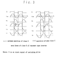
- Fig.3 is an operating waveform diagram of a class E resonance inverter;
- Fig.4 is an operating waveform diagram of the embodiment of the present invention;
- Fig.5 is a partial circuit diagram showing another embodiment of the present invention;
- Fig.6 is a partial circuit diagram showing a further embodiment of the present invention;
- Fig.7 is a circuit diagram of a prior art; and
- Fig.8 is an operating waveform diagram of the prior art
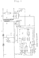
- One preferred embodiment of the present invention will be described in details referring to the accompanying drawings. Fig.1 shows a circuit diagram of an inverter apparatus provided with a load of CFL. As shown in Fig.1, the circuit comprises a power MOSFET Q1, a choke coil L, a coil Lt, a capacitor Ct, and a voltage resonance capacitor Cs, serving as a semi-class E voltage resonance inverter. A high frequency AC voltage from the semi-class E voltage resonance inverter is boosted by a booster transformer T1 and fed to the CFL for direct driving. As known, the semi-class E voltage resonance inverter is capable of producing a sine-wave output as a current across its power switching element has a sine-wave component and a voltage supplied to its switch has a sine-wave form.
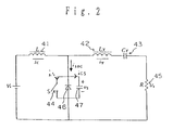
- The principle of action of the semi-class E voltage resonance inverter will now be explained referring to Fig.2. Fig.2 illustrates a basic circuit of the semi-class E voltage resonance inverter. As shown, the choke coil is a
reactor 41 of its current is approximately a direct current Ic. An inductor 42 and acapacitor 43 constitute a resonance circuit. Through turn-on and turn-off actions of aswitch 44, a pulse form of voltage is supplied to a sync circuit including the inductor 42, thecapacitor 43, and aresistor 45. When the (turn on/turn off) action or switching frequency of theswitch 44 is slightly higher than the resonance frequency of the inductor 42 andcapacitor 43, a current iT in the tuning circuit is approximately a sine-wave. In that case, the tuning circuit has an inductive reactance and its current is lagged phase with the phase of voltage. A parallel circuit comprising adiode 46, acapacitor 47, and theswitch 44 has a current isdc of a sine-wave form because Ic=isdc+iT where ir is of a sine-wave form. - Fig.3(a) shows operating waveforms in the class E resonance inverter with the switch having 50% of a duty. When the switch S is turned off, the sine-wave current flows across the capacitor Cs which is then charged with ics and the voltage vs rises up from zero to form a sine-wave. Accordingly, the turn off action of the switch triggers zero voltage, non-zero current switching. The switch voltage vs drops in a near-zero gradient of dvs/dt at an optimum resistance Ropt, as shown in Fig.3(a). When vs=0 and dvs/dt =0, the switch S is turned on. If the resistance is smaller than Ropt, the voltage vs of the switch drops down in a sharp gradient of dvs/dt to zero, as shown in Fig.3(b), and the reverse diode Ds connected in parallel is turned on. While the switch voltage vs being clamped to zero, the switch S is then turn on. This is a semi-class E action implementing zero voltage switching similar to the action of a voltage resonance switch. When the circuit is used as a switching regulator, the class E action cannot be executed throughout the full-scale viable range of load and input voltages but the semi-class E action will be feasible. Since the impedance in an R-L-C tuning circuit is highly responsive to the switching frequency, control of the output voltage Vo (=it) with switching frequency modulation will minimize a change in the switching frequency.
- Returning to Fig.1, the booster transformer T1 comprises a primary coil Np, a secondary coil Ns, and a feedback coil Nf as is connected to the N-channel power MOST Q1 and tne choke coil L. The serial composite impedance of leakage inductance lg of the booster transformer T1, the coil Lt, and the capacitor Ct create a resonance circuit. The resonance circuit is connected in series to the
CFL 1. The resonance frequency Fr of the resonance circuit is then obtained from:
- Referring to Fig.4(b), Toff is determined considering a variation in the performance of the
choke coil 1 and voltage resonance capacitor Cs and a change in the resonance frequency due to thermal variation so that the semi-class E action is successfully carried out. When the oscillation frequency increases with Toff remaining unchanged, the on duration of the switch is decreased thus lowering the input current of the CFL to a constant rate, as shown in Fig.4. If the lamp current drops, the output of the operational amplifier A1 is decreased thus lowering the oscillation frequency of the voltage-controlled oscillator and allowing the supply of a constant current. - For starting a discharging action in the CFL, the CFL has to be loaded with a high voltage of about 1 kV. This release voltage may be set, as shown in Fig.5, by dividing the voltage at the secondary coil Ns of the booster transformer T1 to a divided voltage with two resistors R20 and R21, rectifying it with a combination of a diode D20 and a capacitor C20, and transmitting it to the positive input of the operational amplifier A1 in the voltage resonance switching IC IC1. The disadvantage of this setting is that the resistor R20 of high voltage type is needed and the stable action of non feedback loop will be declined due to a time delay caused by of R20, D20, and C20. For correcting the disadvantage, the booster transformer T1 is provided with a feedback coil Nf as shown in Fig.1. In action, a voltage output of the feedback coil Nf is rectified by a diode D2 and a capacitor C6 and divided voltage by two resistors R10 and R11. A divided output voltage is then transferred through a resistor R9 to the positive input of the operational amplifier A1 in IC1 for feedback. Assuming that the number of windings and the voltage of the secondary coil Ns are Ns and Vs respectively, and the number of windings and the voltage of the feedback coil Nf s are Nf and Vf respectively, the voltage Vs of the secondary coil Ns is expressed by Vs=(Ns/Nf)Vf. Hence, Vs can be maintained constant by controlling Vf regardless of the level of DC voltage to be supplied. Also, Nf may be identical in the level to the input voltage of the operational amplifier A1 thus remaining low and hardly producing any phase delay.
- The collector of a switching transistor Q2 is connected to the joint between the resistors R9, R10, and R11. If CFL1 is disconnected or before the discharge action is started, the voltage across the capacitor C4 is zero and the switching transistor Q2 remains not conducted. Accordingly, the voltage at the secondary coil Ns of the booster transformer T1 is maintained constant regardless of an input level of the DC voltage by the negative feedback action through the resistors R10, R11, and R9 and the operational amplifier A1. When CFL1 is connected and its discharge current flows, the switching transistor Q2 is turned on with the voltage across the capacitor C4 set to more than 0.7 bolts. Accordingly, the resistors R10 and R11 interrupt the constant voltage action and allow only the constant current action with the operational amplifier A1.
- The setting of the release voltage may also be implemented by a circuit shown in Fig.6. As shown, the voltage at the primary coil Np of the booster transformer T1 is detected by a combination of a capacitor CF and a resistor RF, rectified by a diode D20 and a capacitor C20, and divided by two resistors R21 and R22 before transferred to the operational amplifier A1 in IC1.
- As set forth above, the inverter apparatus of the present invention comprises a semi-class E type voltage resonance inverter thus allowing its single power switching element to be operated at a higher efficiency. In addition, the apparatus includes an exclusive inverter circuit and will be composed of a smaller number of components hence contributing to the minimum of the overall dimensions.
Claims (5)
- An inverter apparatus for converting a direct current supplied from a direct current power source to an alternating current by a converting means for alternating between two opposite directions of flow through the on/off actions of its switching element, comprising:a serial resonance circuit provided at the primary side of a booster transformer;a controlling means for turning on and off the serial resonance circuit with the switching element operating at the timing of phase advanced from the resonance frequency of the serial resonance circuit; and a load device connected to the secondary side of the booster transformer.
- An inverter apparatus according to claim 1, further comprising a detecting means provided at the secondary side of the booster transformer for detecting a load so that the controlling means upon receiving a signal output of the detecting means indicative of the load advances the timing phase of the turning on and off actions of the switch element when the load is smaller.
- An inverter apparatus according to claim 1 or 2, where in the load device is a cold cathode tube.
- An inverter apparatus according to claim 3, wherein the booster transformer is coupled to a feedback line for feeding back a voltage to the negative input of an operational amplifier in the controlling means, before the cold cathode tube is connected or a discharge action is started, so as to stabilize a voltage output of the booster transformer.
- An inverter apparatus according to claim 3, wherein the voltage at a primary coil of the booster transformer is fed back to the negative input of an operational amplifier in the controlling means before the cold cathode tube is connected or a discharge action is started so that a voltage output of the booster transformer is stabilized.
Applications Claiming Priority (3)
| Application Number | Priority Date | Filing Date | Title |
|---|---|---|---|
| JP30547194 | 1994-11-15 | ||
| JP30547194A JP3312369B2 (en) | 1994-11-15 | 1994-11-15 | Inverter device |
| JP305471/94 | 1994-11-15 |
Publications (3)
| Publication Number | Publication Date |
|---|---|
| EP0713353A2 true EP0713353A2 (en) | 1996-05-22 |
| EP0713353A3 EP0713353A3 (en) | 1997-05-28 |
| EP0713353B1 EP0713353B1 (en) | 2001-08-01 |
Family
ID=17945556
Family Applications (1)
| Application Number | Title | Priority Date | Filing Date |
|---|---|---|---|
| EP95308087A Expired - Lifetime EP0713353B1 (en) | 1994-11-15 | 1995-11-13 | Inverter apparatus |
Country Status (4)
| Country | Link |
|---|---|
| US (1) | US5818709A (en) |
| EP (1) | EP0713353B1 (en) |
| JP (1) | JP3312369B2 (en) |
| DE (1) | DE69521972T2 (en) |
Cited By (3)
| Publication number | Priority date | Publication date | Assignee | Title |
|---|---|---|---|---|
| EP0735658A2 (en) * | 1995-03-31 | 1996-10-02 | Minebea Co.,Ltd. | Inverter unit |
| EP0802702A2 (en) * | 1996-04-16 | 1997-10-22 | O2 Micro, Inc. | Higher-efficiency cold-cathode fluorescent lamp power supply |
| WO1998028949A1 (en) * | 1996-12-23 | 1998-07-02 | Koninklijke Philips Electronics N.V. | Ballast circuit |
Families Citing this family (13)
| Publication number | Priority date | Publication date | Assignee | Title |
|---|---|---|---|---|
| JP3238088B2 (en) * | 1996-12-17 | 2001-12-10 | 日本電気株式会社 | Piezoelectric transformer drive circuit and cold cathode tube lighting device using the same |
| US5978244A (en) | 1997-10-16 | 1999-11-02 | Illinois Tool Works, Inc. | Programmable logic control system for a HVDC power supply |
| US6144570A (en) * | 1997-10-16 | 2000-11-07 | Illinois Tool Works Inc. | Control system for a HVDC power supply |
| US6144173A (en) * | 1999-11-10 | 2000-11-07 | General Electric Company | Single switch electronic ballast |
| WO2002087290A1 (en) * | 2001-04-20 | 2002-10-31 | Koninklijke Philips Electronics N.V. | Circuit arrangement for discharge lamp comprising a resonant half-bridge converter driven by a class-e driver |
| US7109665B2 (en) * | 2002-06-05 | 2006-09-19 | International Rectifier Corporation | Three-way dimming CFL ballast |
| KR100616538B1 (en) * | 2004-01-05 | 2006-08-29 | 삼성전기주식회사 | Single stage back-light inverter, and driving method thereof |
| US7332871B2 (en) * | 2005-04-04 | 2008-02-19 | Chao-Cheng Lu | High frequency power source control circuit and protective circuit apparatus |
| US7619368B2 (en) * | 2005-07-05 | 2009-11-17 | Chao-Cheng Lu | Power source apparatus |
| US7498751B2 (en) * | 2006-06-15 | 2009-03-03 | Himax Technologies Limited | High efficiency and low cost cold cathode fluorescent lamp driving apparatus for LCD backlight |
| JP2014528688A (en) * | 2011-10-14 | 2014-10-27 | インディス、プロプライエタリー、リミテッドIndice Pty Ltd | Power control |
| KR101768598B1 (en) * | 2014-09-11 | 2017-08-17 | 한국전기연구원 | Circuit of Voltage Sensing and Controlling |
| WO2019202352A1 (en) * | 2018-04-20 | 2019-10-24 | 日産自動車株式会社 | Control method for controlling resonant power converter, and resonant power converter |
Family Cites Families (12)
| Publication number | Priority date | Publication date | Assignee | Title |
|---|---|---|---|---|
| US3919656A (en) * | 1973-04-23 | 1975-11-11 | Nathan O Sokal | High-efficiency tuned switching power amplifier |
| US4492899A (en) * | 1981-08-18 | 1985-01-08 | Indicator Controls Corporation | Solid state regulated power supply system for cold cathode luminous tube |
| US4532456A (en) * | 1982-07-12 | 1985-07-30 | Gte Products Corporation | Output circuit for an electronic ballast system |
| US4607323A (en) * | 1984-04-17 | 1986-08-19 | Sokal Nathan O | Class E high-frequency high-efficiency dc/dc power converter |
| DE3427493A1 (en) * | 1984-07-26 | 1986-01-30 | Philips Patentverwaltung Gmbh, 2000 Hamburg | CIRCUIT ARRANGEMENT FOR SWITCHING A CURRENT IN AN INDUCTIVE LOAD |
| US4651271A (en) * | 1985-04-25 | 1987-03-17 | Power Modifications Incorporated | Power supply having tuned radio frequency circuit |
| GB2177273A (en) * | 1985-06-26 | 1987-01-14 | Philips Electronic Associated | R f power amplifier |
| US4814962A (en) * | 1988-05-27 | 1989-03-21 | American Telephone And Telegraph Company, At&T Bell Laboratories | Zero voltage switching half bridge resonant converter |
| US5068570A (en) * | 1989-01-26 | 1991-11-26 | Koito Manufacturing Co., Ltd. | Lamp lighting circuit with an overload protection capability |
| US5065300A (en) * | 1991-03-08 | 1991-11-12 | Raytheon Company | Class E fixed frequency converter |
| US5159541A (en) * | 1991-10-31 | 1992-10-27 | Northern Telecom Limited | Asymmetrical pulse width modulated resonant DC/DC converter |
| US5315214A (en) * | 1992-06-10 | 1994-05-24 | Metcal, Inc. | Dimmable high power factor high-efficiency electronic ballast controller integrated circuit with automatic ambient over-temperature shutdown |
-
1994
- 1994-11-15 JP JP30547194A patent/JP3312369B2/en not_active Expired - Fee Related
-
1995
- 1995-11-13 EP EP95308087A patent/EP0713353B1/en not_active Expired - Lifetime
- 1995-11-13 DE DE69521972T patent/DE69521972T2/en not_active Expired - Fee Related
- 1995-11-14 US US08/555,708 patent/US5818709A/en not_active Expired - Fee Related
Non-Patent Citations (1)
| Title |
|---|
| None |
Cited By (5)
| Publication number | Priority date | Publication date | Assignee | Title |
|---|---|---|---|---|
| EP0735658A2 (en) * | 1995-03-31 | 1996-10-02 | Minebea Co.,Ltd. | Inverter unit |
| EP0735658A3 (en) * | 1995-03-31 | 1997-06-04 | Minebea Co Ltd | Inverter unit |
| EP0802702A2 (en) * | 1996-04-16 | 1997-10-22 | O2 Micro, Inc. | Higher-efficiency cold-cathode fluorescent lamp power supply |
| EP0802702A3 (en) * | 1996-04-16 | 1998-11-04 | O2 Micro, Inc. | Higher-efficiency cold-cathode fluorescent lamp power supply |
| WO1998028949A1 (en) * | 1996-12-23 | 1998-07-02 | Koninklijke Philips Electronics N.V. | Ballast circuit |
Also Published As
| Publication number | Publication date |
|---|---|
| JPH08149823A (en) | 1996-06-07 |
| EP0713353A3 (en) | 1997-05-28 |
| DE69521972D1 (en) | 2001-09-06 |
| EP0713353B1 (en) | 2001-08-01 |
| DE69521972T2 (en) | 2001-12-20 |
| US5818709A (en) | 1998-10-06 |
| JP3312369B2 (en) | 2002-08-05 |
Similar Documents
| Publication | Publication Date | Title |
|---|---|---|
| US5666279A (en) | Voltage resonance inverter circuit for dimable cold cathode tubes | |
| EP0735658B1 (en) | Inverter unit | |
| US5818709A (en) | Inverter apparatus | |
| US8581518B2 (en) | Triac dimmer compatible switching mode power supply and method thereof | |
| US5434477A (en) | Circuit for powering a fluorescent lamp having a transistor common to both inverter and the boost converter and method for operating such a circuit | |
| US5416387A (en) | Single stage, high power factor, gas discharge lamp ballast | |
| US4677534A (en) | Stabilizing power source apparatus | |
| US20170063242A1 (en) | Control method and device employing primary side regulation in a quasi-resonant ac/dc flyback converter | |
| US5834907A (en) | Cold cathode tube operating apparatus with piezoelectric transformer | |
| KR20040080985A (en) | Switching constant-current power supply system | |
| JPH07298636A (en) | Self-excited inverter | |
| JPH0973990A (en) | Cold cathode tube lighting device using piezo-electric transformer | |
| KR0137181B1 (en) | Discharge lamp lighting device | |
| JPH03212171A (en) | Switching power supply for microwave oven | |
| JPH08149850A (en) | Voltage converter | |
| KR100745305B1 (en) | Adaptor using step-down piezoelectric transformer | |
| US6936974B2 (en) | Half-bridge inverter for asymmetrical loads | |
| US20050062439A1 (en) | Dimming control techniques using self-excited gate circuits | |
| JPH06327257A (en) | Power device | |
| JP2001128457A (en) | Power supply | |
| JP3304534B2 (en) | Discharge lamp lighting device | |
| JP2868224B2 (en) | Load control device | |
| JPH05316740A (en) | Inverter | |
| JPH066478Y2 (en) | Inverter for lighting EL lamp | |
| JP3331713B2 (en) | Power supply |
Legal Events
| Date | Code | Title | Description |
|---|---|---|---|
| PUAI | Public reference made under article 153(3) epc to a published international application that has entered the european phase |
Free format text: ORIGINAL CODE: 0009012 |
|
| AK | Designated contracting states |
Kind code of ref document: A2 Designated state(s): DE FR GB IT |
|
| PUAL | Search report despatched |
Free format text: ORIGINAL CODE: 0009013 |
|
| AK | Designated contracting states |
Kind code of ref document: A3 Designated state(s): DE FR GB IT |
|
| 17P | Request for examination filed |
Effective date: 19971120 |
|
| GRAG | Despatch of communication of intention to grant |
Free format text: ORIGINAL CODE: EPIDOS AGRA |
|
| 17Q | First examination report despatched |
Effective date: 20000822 |
|
| GRAG | Despatch of communication of intention to grant |
Free format text: ORIGINAL CODE: EPIDOS AGRA |
|
| GRAH | Despatch of communication of intention to grant a patent |
Free format text: ORIGINAL CODE: EPIDOS IGRA |
|
| GRAG | Despatch of communication of intention to grant |
Free format text: ORIGINAL CODE: EPIDOS AGRA |
|
| GRAH | Despatch of communication of intention to grant a patent |
Free format text: ORIGINAL CODE: EPIDOS IGRA |
|
| RIC1 | Information provided on ipc code assigned before grant |
Free format text: 7H 05B 41/295 A, 7H 05B 41/392 B, 7H 02M 7/537 B |
|
| GRAH | Despatch of communication of intention to grant a patent |
Free format text: ORIGINAL CODE: EPIDOS IGRA |
|
| GRAA | (expected) grant |
Free format text: ORIGINAL CODE: 0009210 |
|
| AK | Designated contracting states |
Kind code of ref document: B1 Designated state(s): DE FR GB IT |
|
| PG25 | Lapsed in a contracting state [announced via postgrant information from national office to epo] |
Ref country code: IT Free format text: LAPSE BECAUSE OF FAILURE TO SUBMIT A TRANSLATION OF THE DESCRIPTION OR TO PAY THE FEE WITHIN THE PRE;WARNING: LAPSES OF ITALIAN PATENTS WITH EFFECTIVE DATE BEFORE 2007 MAY HAVE OCCURRED AT ANY TIME BEFORE 2007. THE CORRECT EFFECTIVE DATE MAY BE DIFFERENT FROM THE ONE RECORDED.SCRIBED TIME-LIMIT Effective date: 20010801 Ref country code: FR Free format text: LAPSE BECAUSE OF FAILURE TO SUBMIT A TRANSLATION OF THE DESCRIPTION OR TO PAY THE FEE WITHIN THE PRESCRIBED TIME-LIMIT Effective date: 20010801 |
|
| REF | Corresponds to: |
Ref document number: 69521972 Country of ref document: DE Date of ref document: 20010906 |
|
| EN | Fr: translation not filed | ||
| REG | Reference to a national code |
Ref country code: GB Ref legal event code: IF02 |
|
| PLBE | No opposition filed within time limit |
Free format text: ORIGINAL CODE: 0009261 |
|
| STAA | Information on the status of an ep patent application or granted ep patent |
Free format text: STATUS: NO OPPOSITION FILED WITHIN TIME LIMIT |
|
| 26N | No opposition filed | ||
| PGFP | Annual fee paid to national office [announced via postgrant information from national office to epo] |
Ref country code: DE Payment date: 20030403 Year of fee payment: 8 |
|
| PG25 | Lapsed in a contracting state [announced via postgrant information from national office to epo] |
Ref country code: DE Free format text: LAPSE BECAUSE OF NON-PAYMENT OF DUE FEES Effective date: 20040602 |
|
| PGFP | Annual fee paid to national office [announced via postgrant information from national office to epo] |
Ref country code: GB Payment date: 20061108 Year of fee payment: 12 |
|
| GBPC | Gb: european patent ceased through non-payment of renewal fee |
Effective date: 20071113 |
|
| PG25 | Lapsed in a contracting state [announced via postgrant information from national office to epo] |
Ref country code: GB Free format text: LAPSE BECAUSE OF NON-PAYMENT OF DUE FEES Effective date: 20071113 |