EP0713245A2 - A heat treatment jig for semiconductor wafers and a method for treating a surface of the same - Google Patents
A heat treatment jig for semiconductor wafers and a method for treating a surface of the same Download PDFInfo
- Publication number
- EP0713245A2 EP0713245A2 EP95118090A EP95118090A EP0713245A2 EP 0713245 A2 EP0713245 A2 EP 0713245A2 EP 95118090 A EP95118090 A EP 95118090A EP 95118090 A EP95118090 A EP 95118090A EP 0713245 A2 EP0713245 A2 EP 0713245A2
- Authority
- EP
- European Patent Office
- Prior art keywords
- heat treatment
- silicon
- nitride layer
- treatment jig
- silicon nitride
- Prior art date
- Legal status (The legal status is an assumption and is not a legal conclusion. Google has not performed a legal analysis and makes no representation as to the accuracy of the status listed.)
- Withdrawn
Links
Images
Classifications
-
- C—CHEMISTRY; METALLURGY
- C04—CEMENTS; CONCRETE; ARTIFICIAL STONE; CERAMICS; REFRACTORIES
- C04B—LIME, MAGNESIA; SLAG; CEMENTS; COMPOSITIONS THEREOF, e.g. MORTARS, CONCRETE OR LIKE BUILDING MATERIALS; ARTIFICIAL STONE; CERAMICS; REFRACTORIES; TREATMENT OF NATURAL STONE
- C04B41/00—After-treatment of mortars, concrete, artificial stone or ceramics; Treatment of natural stone
- C04B41/80—After-treatment of mortars, concrete, artificial stone or ceramics; Treatment of natural stone of only ceramics
- C04B41/81—Coating or impregnation
- C04B41/85—Coating or impregnation with inorganic materials
- C04B41/87—Ceramics
-
- C—CHEMISTRY; METALLURGY
- C04—CEMENTS; CONCRETE; ARTIFICIAL STONE; CERAMICS; REFRACTORIES
- C04B—LIME, MAGNESIA; SLAG; CEMENTS; COMPOSITIONS THEREOF, e.g. MORTARS, CONCRETE OR LIKE BUILDING MATERIALS; ARTIFICIAL STONE; CERAMICS; REFRACTORIES; TREATMENT OF NATURAL STONE
- C04B41/00—After-treatment of mortars, concrete, artificial stone or ceramics; Treatment of natural stone
- C04B41/45—Coating or impregnating, e.g. injection in masonry, partial coating of green or fired ceramics, organic coating compositions for adhering together two concrete elements
- C04B41/50—Coating or impregnating, e.g. injection in masonry, partial coating of green or fired ceramics, organic coating compositions for adhering together two concrete elements with inorganic materials
- C04B41/5053—Coating or impregnating, e.g. injection in masonry, partial coating of green or fired ceramics, organic coating compositions for adhering together two concrete elements with inorganic materials non-oxide ceramics
- C04B41/5062—Borides, Nitrides or Silicides
- C04B41/5066—Silicon nitride
-
- C—CHEMISTRY; METALLURGY
- C04—CEMENTS; CONCRETE; ARTIFICIAL STONE; CERAMICS; REFRACTORIES
- C04B—LIME, MAGNESIA; SLAG; CEMENTS; COMPOSITIONS THEREOF, e.g. MORTARS, CONCRETE OR LIKE BUILDING MATERIALS; ARTIFICIAL STONE; CERAMICS; REFRACTORIES; TREATMENT OF NATURAL STONE
- C04B41/00—After-treatment of mortars, concrete, artificial stone or ceramics; Treatment of natural stone
- C04B41/45—Coating or impregnating, e.g. injection in masonry, partial coating of green or fired ceramics, organic coating compositions for adhering together two concrete elements
- C04B41/52—Multiple coating or impregnating multiple coating or impregnating with the same composition or with compositions only differing in the concentration of the constituents, is classified as single coating or impregnation
-
- C—CHEMISTRY; METALLURGY
- C04—CEMENTS; CONCRETE; ARTIFICIAL STONE; CERAMICS; REFRACTORIES
- C04B—LIME, MAGNESIA; SLAG; CEMENTS; COMPOSITIONS THEREOF, e.g. MORTARS, CONCRETE OR LIKE BUILDING MATERIALS; ARTIFICIAL STONE; CERAMICS; REFRACTORIES; TREATMENT OF NATURAL STONE
- C04B41/00—After-treatment of mortars, concrete, artificial stone or ceramics; Treatment of natural stone
- C04B41/80—After-treatment of mortars, concrete, artificial stone or ceramics; Treatment of natural stone of only ceramics
- C04B41/81—Coating or impregnation
- C04B41/89—Coating or impregnation for obtaining at least two superposed coatings having different compositions
-
- C—CHEMISTRY; METALLURGY
- C30—CRYSTAL GROWTH
- C30B—SINGLE-CRYSTAL GROWTH; UNIDIRECTIONAL SOLIDIFICATION OF EUTECTIC MATERIAL OR UNIDIRECTIONAL DEMIXING OF EUTECTOID MATERIAL; REFINING BY ZONE-MELTING OF MATERIAL; PRODUCTION OF A HOMOGENEOUS POLYCRYSTALLINE MATERIAL WITH DEFINED STRUCTURE; SINGLE CRYSTALS OR HOMOGENEOUS POLYCRYSTALLINE MATERIAL WITH DEFINED STRUCTURE; AFTER-TREATMENT OF SINGLE CRYSTALS OR A HOMOGENEOUS POLYCRYSTALLINE MATERIAL WITH DEFINED STRUCTURE; APPARATUS THEREFOR
- C30B35/00—Apparatus not otherwise provided for, specially adapted for the growth, production or after-treatment of single crystals or of a homogeneous polycrystalline material with defined structure
Definitions
- This invention relates to a heat treatment jig for semiconductor wafers and a method for treating a surface of the same, and more particularly, to a heat treatment jig for semiconductor wafers such as single crystal wafers without causing contamination when using in the heat treatment and a method for treating a surface of the same.
- silicon materials and such are used for manufacturing high performance VLSIs, ULSIs, etc. These silicon materials are wafer-shaped, generally called a silicon single crystal wafer. The desired devices are formed on the surface or near the surface of the silicon single crystal wafer.
- a high temperature heat treatment called a high temperature annealing
- a silicon single crystal wafer which is placed on a heat treatment jig, i.e. a wafer boat is inserted into a heat treatment furnace and heated to a high temperature.
- a high temperature annealing in a hydrogen ambience is effective for complete denudation of the vicinity of the surface of semiconductor wafers.
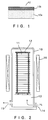
- FIG. 2 shows one example of a vertical-type heat treatment furnace used for the high temperature annealing.
- a tube 10 contains a boat supporting mount 13 on which a wafer boat 12 is placed.
- a plurality of silicon single crystal wafers 11 are held on the wafer boat 12.
- the temperature is increased up to 1,200°C by a heater 16, while ambient gas is supplied through a gas introduction port 14.
- the ambient gas goes out through a gas exhaust port 15 after the annealing.
- Examples of the material of the wafer boat 12 used for the high temperature annealing include quartz, silicon and silicon carbide.
- a wafer boat made of quartz has an advantage of a higher level cleanliness, but also has a disadvantages in that it is prone to deformation because softening occurs at temperatures higher than 1,140°C.
- a wafer boat made of silicon has an advantage in reducing slippage of the silicon single crystal wafers during the heat treatment, but also has a disadvantage in that it sticks to the silicon single crystal wafers which are made of the same material at temperatures higher than 1,100°C.
- a wafer boat made of silicon carbide has an advantage in having enough strength, but has a disadvantage of low level cleanliness due to the diffusion of impurities from inside the wafer boat.
- the protective layer deposited by CVD has minute holes such as so-called pin-holes, and it is insufficient for preventing the out-diffusion of impurities from inside the wafer boat. Additionally, the minute holes tend to develop into cracks during the high temperature annealing, and the particles may contaminate the wafer surface.
- a wafer boat which is used in in so-called hydrogen annealing in which a hydrogen ambience is introduced during the high temperature annealing, is coated with silicon oxide as a protective layer deposited by CVD and or is made of quartz, there generates water by a reaction between the oxygen which composes the protective layer or boat materials and hydrogen, and then the water reacts with the wafer and the surface silicon of the silicon single crystal wafer, resulting in generation of pit-like defects.
- the object of the invention is to provide a heat treatment jig for semiconductor wafers without sticking to the semiconductor wafers.
- the another object of the invention is to provide a heat treatment jig for semiconductor wafers by which the out-diffusion of impurities from the heat treatment jig is controlled sufficiently and easily
- the further object of the invention is to provide a heat treatment jig for semiconductor wafers by which harmful effects such as the generation of pit-like defects is prevented during hydrogen annealing.
- a silicon nitride layer is thermally grown on the topmost surface of the heat treatment jig composed of silicon or silicon carbide in a nitrogen ambient.
- Said silicon nitride layer may be thermally grown on the surface of a protective layer deposited with CVD on the heat treatment jig.
- a silicon nitride layer is thermally grown on a surface of the heat treatment jig composed of silicon or silicon carbide in a nitrogen ambient in the temperature range of 1,100°C-1,300°C.
- the silicon nitride layer is thermally grown on the wafer boat surface in a nitrogen ambience.
- the silicon nitride layer is a dense layer, compared with a silicon nitride layer deposited with CVD, and it possible to prevent the diffusion of metallic impurities from the inside the wafer boat to the outside. Also, since the thermally grown silicon nitride layer is different from the wafer material, it does not stick to the silicon single crystal wafer during the high temperature annealing.
- the wafer boat surface is slightly etched (hydrogen etching) and the impurity-containing layer on said surface is removed and the surface is made active.
- a clean and dense silicon nitride layer can be formed by conducting a heat treatment on the active surface directly in a nitrogen ambience.
- a thicker silicon nitride layer can be formed by forming a silicon oxide layer by a heat treatment in an oxygen ambience after the hydrogen etching and before forming a silicon nitride layer.
- this silicon nitride layer can be thermally grown in a simple process to obtain a denser layer than the silicon nitride layer deposited by CVD, and therefore it is less prone to reaction during the hydrogen annealing, its effect of preventing impurity diffusion lasts longer, and it assures the prevention of contamination of the silicon single crystal wafer by impurities.
- Figure 1 is a partial cross section showing one example of the semiconductor heat treatment jig of the present invent ion.
- Figure 2 is a schematic cross section showing an example of the vertical-type heat treatment furnace used for the hydrogen annealing.
- a heat treatment of the wafer boat 12 made of silicon carbide was conducted in a hydrogen ambience, and then the silicon nitride layer 12b was formed on the surface of the silicon carbide 12a, as shown in Figure 1.
- the wafer boat 12 was inserted in the vertical-type heat treatment furnace. After slightly etching the surface (0.1 micrometers) with a 2-hour heat treatment in a hydrogen ambience at 1,200°C, a 1-hour heat treatment in a nitrogen ambience at 1,200°C was conducted to form the silicon nitride layer 12b with a thickness of approximately 1 micrometer on the wafer boat 12.
- the CZ silicon single crystal wafers 11 were placed on the wafer boat 12 and then inserted in the vertical-type heat treatment furnace for 1 hour of hydrogen annealing at 1,200°C.
- the concentration of each of the metallic impurities, Cu, Fe, Cr and Ni, on the surfaces of the silicon single crystal wafers was measured using induced plasma mass spectroscopy (ICP-MS).
- the wafer boat 12 made of silicon carbide which has a surface protective layer formed by CVD was inserted in the vertical-type heat treatment furnace. After the surface was given hydrogen etching under the same conditions as in Example 1, a silicon nitride layer was formed. Using this wafer boat 12, the CZ silicon single crystal wafers 11 were placed on the wafer boat 12 and then inserted in the vertical-type heat treatment furnace for hydrogen annealing under the same conditions as in Example 1. The concentration of each of the metallic impurities, Cu, Fe, Cr and Ni, on the surfaces of the silicon single crystal wafers was measured using ICP-MS.
- the silicon oxide layer was thermally grown and a heat treatment was conducted on the surface of the wafer boat 12 in a nitrogen ambience to form a silicon nitride layer.
- the wafer boat 12 was inserted in the vertical-type heat treatment furnace. After slightly etching the surface (0.1 micrometers) with a 2-hour heat treatment in a hydrogen ambience at 1,200°C, the wafer boat 12 was once taken out and the ambience in the furnace was replaced by a nitrogen ambience and then by a dry oxygen ambience.
- the wafer boat 12 was inserted again and a 2-hour heat treatment at 1,200°C was conducted to form an approximately 0.5 micrometer-thick silicon oxide layer, and then a 1-hour heat treatment in a nitrogen ambience at 1,200°C was conducted to form an approximately 1.2 micrometer-thick silicon nitride layer on the wafer boat 12.
- the CZ silicon single crystal wafers 11 were placed on the wafer boat 12 and then inserted in the vertical-type heat treatment furnace for 1 hour of hydrogen annealing at 1,200°C.
- the concentration of each of the metallic impurities, Cu, Fe, Cr and Ni, on the surfaces of the silicon single crystal wafers was measured using ICP-MS.
- the CZ silicon single crystal wafers 11 were placed on the wafer boat 12 and then inserted in the vertical -type heat treatment furnace for hydrogen annealing under the same conditions as in Example 1.
- the concentration of each of the metallic impurities, Cu, Fe, Cr and Ni, on the surfaces of the silicon single crystal wafers was measured using ICP-MS.
- the CZ silicon single crystal wafers 11 were placed on the wafer boat 12 and then inserted in the vertical-type heat treatment furnace for hydrogen annealing under the same conditions as in Example 1.
- the concentration of each of the metallic impurities, Cu, Fe, Cr and Ni, on the surfaces of the silicon single crystal wafers was measured using ICP-MS.
- each Example has reduced concentrations of the metallic impurities compared with each Comparative example. Thus, it is confirmed that the out-diffusion of impurities from the heat treatment jig is suppressed in the Examples.
- the present invention has an effect of reducing the out-diffusion of impurities from the material of the heat treatment jig by thermally growing a silicon nitride layer on the surface of the heat treatment jig.
- the silicon wafers with 1-hour hydrogen annealing at 1,200°C using this heat treatment jig showed a reduction to approximately a tenth of the concentrations of Cu and Fe, and also a substantial reduction in the concentrations of Cr and Ni.
Abstract
Description
- This application claims the priority of Japanese Patent application No. 6-308243 filed on November 17, 1994, which is incorporated herein by reference.
- This invention relates to a heat treatment jig for semiconductor wafers and a method for treating a surface of the same, and more particularly, to a heat treatment jig for semiconductor wafers such as single crystal wafers without causing contamination when using in the heat treatment and a method for treating a surface of the same.
- In a manufacturing process of semiconductor devices, silicon materials and such are used for manufacturing high performance VLSIs, ULSIs, etc. These silicon materials are wafer-shaped, generally called a silicon single crystal wafer. The desired devices are formed on the surface or near the surface of the silicon single crystal wafer.
- There are crystal defects related to interstitial oxygen and such existing in the silicon single crystal wafer, and it is necessary to remove the crystal defects near the wafer surface where the devices are formed. In order to denude the crystal defects near the wafer surface, a high temperature heat treatment, called a high temperature annealing, is adopted in which a silicon single crystal wafer which is placed on a heat treatment jig, i.e. a wafer boat is inserted into a heat treatment furnace and heated to a high temperature. In recent years, it has been found that a high temperature annealing in a hydrogen ambience is effective for complete denudation of the vicinity of the surface of semiconductor wafers.
- Figure 2 shows one example of a vertical-type heat treatment furnace used for the high temperature annealing. In this figure, a
tube 10 contains aboat supporting mount 13 on which awafer boat 12 is placed. A plurality of siliconsingle crystal wafers 11 are held on thewafer boat 12. When conducting the high temperature annealing of the siliconsingle crystal wafers 11, the temperature is increased up to 1,200°C by aheater 16, while ambient gas is supplied through agas introduction port 14. The ambient gas goes out through agas exhaust port 15 after the annealing. - Examples of the material of the
wafer boat 12 used for the high temperature annealing include quartz, silicon and silicon carbide. A wafer boat made of quartz has an advantage of a higher level cleanliness, but also has a disadvantages in that it is prone to deformation because softening occurs at temperatures higher than 1,140°C. A wafer boat made of silicon has an advantage in reducing slippage of the silicon single crystal wafers during the heat treatment, but also has a disadvantage in that it sticks to the silicon single crystal wafers which are made of the same material at temperatures higher than 1,100°C. A wafer boat made of silicon carbide has an advantage in having enough strength, but has a disadvantage of low level cleanliness due to the diffusion of impurities from inside the wafer boat. - To prevent such problems, a method has been proposed in which a protective layer is deposited on the surface of the wafer boat by the chemical vapor deposition (CVD).
- However, the protective layer deposited by CVD has minute holes such as so-called pin-holes, and it is insufficient for preventing the out-diffusion of impurities from inside the wafer boat. Additionally, the minute holes tend to develop into cracks during the high temperature annealing, and the particles may contaminate the wafer surface.
- Furthermore, if a wafer boat, which is used in in so-called hydrogen annealing in which a hydrogen ambience is introduced during the high temperature annealing, is coated with silicon oxide as a protective layer deposited by CVD and or is made of quartz, there generates water by a reaction between the oxygen which composes the protective layer or boat materials and hydrogen, and then the water reacts with the wafer and the surface silicon of the silicon single crystal wafer, resulting in generation of pit-like defects.
- The object of the invention is to provide a heat treatment jig for semiconductor wafers without sticking to the semiconductor wafers.
- The another object of the invention is to provide a heat treatment jig for semiconductor wafers by which the out-diffusion of impurities from the heat treatment jig is controlled sufficiently and easily
- The further object of the invention is to provide a heat treatment jig for semiconductor wafers by which harmful effects such as the generation of pit-like defects is prevented during hydrogen annealing.
- In order to solve the problems described above, in the heat treatment jig of the present invention, a silicon nitride layer is thermally grown on the topmost surface of the heat treatment jig composed of silicon or silicon carbide in a nitrogen ambient.
- Said silicon nitride layer may be thermally grown on the surface of a protective layer deposited with CVD on the heat treatment jig.
- In the surface treatment method of the heat treatment jig of the present invention, a silicon nitride layer is thermally grown on a surface of the heat treatment jig composed of silicon or silicon carbide in a nitrogen ambient in the temperature range of 1,100°C-1,300°C.
- In this method, it is desirable to remove slightly the surface of the heat treatment jig by etching before thermally growing the silicon nitride layer. It is desirable to conduct the etching by introducing hydrogen gas at a high temperature (hereafter referred to as "hydrogen etching"). Also, it is desirable to form said silicon nitride layer after etching the surface of the heat treatment jig and then thermally growing a silicon oxide layer in an oxygen ambience.
- In the present invention, the silicon nitride layer is thermally grown on the wafer boat surface in a nitrogen ambience. The silicon nitride layer is a dense layer, compared with a silicon nitride layer deposited with CVD, and it possible to prevent the diffusion of metallic impurities from the inside the wafer boat to the outside. Also, since the thermally grown silicon nitride layer is different from the wafer material, it does not stick to the silicon single crystal wafer during the high temperature annealing.
- If the heat treatment is conducted in a hydrogen ambience, the wafer boat surface is slightly etched (hydrogen etching) and the impurity-containing layer on said surface is removed and the surface is made active. A clean and dense silicon nitride layer can be formed by conducting a heat treatment on the active surface directly in a nitrogen ambience. A thicker silicon nitride layer can be formed by forming a silicon oxide layer by a heat treatment in an oxygen ambience after the hydrogen etching and before forming a silicon nitride layer.
- Furthermore, this silicon nitride layer can be thermally grown in a simple process to obtain a denser layer than the silicon nitride layer deposited by CVD, and therefore it is less prone to reaction during the hydrogen annealing, its effect of preventing impurity diffusion lasts longer, and it assures the prevention of contamination of the silicon single crystal wafer by impurities.
- Figure 1 is a partial cross section showing one example of the semiconductor heat treatment jig of the present invent ion.
- Figure 2 is a schematic cross section showing an example of the vertical-type heat treatment furnace used for the hydrogen annealing.
- The present invention is described in detail below by referring to examples. Specific examples of the present invention are described below.
- Using a vertical-type heat treatment furnace shown in Figure 2, a heat treatment of the
wafer boat 12 made of silicon carbide was conducted in a hydrogen ambience, and then thesilicon nitride layer 12b was formed on the surface of thesilicon carbide 12a, as shown in Figure 1. In detail, thewafer boat 12 was inserted in the vertical-type heat treatment furnace. After slightly etching the surface (0.1 micrometers) with a 2-hour heat treatment in a hydrogen ambience at 1,200°C, a 1-hour heat treatment in a nitrogen ambience at 1,200°C was conducted to form thesilicon nitride layer 12b with a thickness of approximately 1 micrometer on thewafer boat 12. Using thiswafer boat 12, the CZ siliconsingle crystal wafers 11 were placed on thewafer boat 12 and then inserted in the vertical-type heat treatment furnace for 1 hour of hydrogen annealing at 1,200°C. The concentration of each of the metallic impurities, Cu, Fe, Cr and Ni, on the surfaces of the silicon single crystal wafers was measured using induced plasma mass spectroscopy (ICP-MS). - The
wafer boat 12 made of silicon carbide which has a surface protective layer formed by CVD was inserted in the vertical-type heat treatment furnace. After the surface was given hydrogen etching under the same conditions as in Example 1, a silicon nitride layer was formed. Using thiswafer boat 12, the CZ siliconsingle crystal wafers 11 were placed on thewafer boat 12 and then inserted in the vertical-type heat treatment furnace for hydrogen annealing under the same conditions as in Example 1. The concentration of each of the metallic impurities, Cu, Fe, Cr and Ni, on the surfaces of the silicon single crystal wafers was measured using ICP-MS. - After conducting the hydrogen etching on the
wafer boat 12 made of silicon carbide, the silicon oxide layer was thermally grown and a heat treatment was conducted on the surface of thewafer boat 12 in a nitrogen ambience to form a silicon nitride layer. In detail, thewafer boat 12 was inserted in the vertical-type heat treatment furnace. After slightly etching the surface (0.1 micrometers) with a 2-hour heat treatment in a hydrogen ambience at 1,200°C, thewafer boat 12 was once taken out and the ambience in the furnace was replaced by a nitrogen ambience and then by a dry oxygen ambience. Thewafer boat 12 was inserted again and a 2-hour heat treatment at 1,200°C was conducted to form an approximately 0.5 micrometer-thick silicon oxide layer, and then a 1-hour heat treatment in a nitrogen ambience at 1,200°C was conducted to form an approximately 1.2 micrometer-thick silicon nitride layer on thewafer boat 12. Using thiswafer boat 12 with the surface treatments, the CZ siliconsingle crystal wafers 11 were placed on thewafer boat 12 and then inserted in the vertical-type heat treatment furnace for 1 hour of hydrogen annealing at 1,200°C. The concentration of each of the metallic impurities, Cu, Fe, Cr and Ni, on the surfaces of the silicon single crystal wafers was measured using ICP-MS. - Using the
wafer boat 12 made of silicon carbide, the CZ siliconsingle crystal wafers 11 were placed on thewafer boat 12 and then inserted in the vertical -type heat treatment furnace for hydrogen annealing under the same conditions as in Example 1. The concentration of each of the metallic impurities, Cu, Fe, Cr and Ni, on the surfaces of the silicon single crystal wafers was measured using ICP-MS. - Using the
wafer boat 12 made of silicon carbide which has a surface protective layer formed by the CVD method, the CZ siliconsingle crystal wafers 11 were placed on thewafer boat 12 and then inserted in the vertical-type heat treatment furnace for hydrogen annealing under the same conditions as in Example 1. The concentration of each of the metallic impurities, Cu, Fe, Cr and Ni, on the surfaces of the silicon single crystal wafers was measured using ICP-MS. - The measurements of the concentration of each of the metallic impurities, i.e. Cu, Fe, Cr and Ni, on the wafer surfaces treated in Example 1, Example 2, Comparative example 1 and Comparative example 2 are shown in Table 1.

- As shown in Table 1, each Example has reduced concentrations of the metallic impurities compared with each Comparative example. Thus, it is confirmed that the out-diffusion of impurities from the heat treatment jig is suppressed in the Examples.
- As described thus far, the present invention has an effect of reducing the out-diffusion of impurities from the material of the heat treatment jig by thermally growing a silicon nitride layer on the surface of the heat treatment jig. For example, the silicon wafers with 1-hour hydrogen annealing at 1,200°C using this heat treatment jig showed a reduction to approximately a tenth of the concentrations of Cu and Fe, and also a substantial reduction in the concentrations of Cr and Ni.
Claims (5)
- A heat treatment jig for semiconductor wafers:
wherein said heat treatment jig consists of silicon or silicon carbide; and
a silicon nitride layer is provided on the topmost surface of the heat treatment jig, said silicon nitride layer being thermally grown in a nitrogen ambience. - A method for a surface treatment of a heat treatment jig for semiconductor wafers:
wherein a silicon nitride layer is thermally grown on a surface of the heat treatment jig composed of silicon or silicon carbide in a nitrogen ambience in the temperature range of 1,100°C-1,300°C. - A method for a surface treatment of a heat treatment jig for semiconductor wafers according to Claim 2:
wherein the surface layer of said heat treatment jig is removed slightly by etching before thermally growing said silicon nitride layer. - A method for a surface treatment of a heat treatment jig for semiconductor wafers according to Claim 3:
wherein said etching is conducted by introducing hydrogen gas in a high temperature ambience. - A method for a surface treatment of a heat treatment jig for semiconductor wafers according to Claim 3 or 4:
wherein a silicon oxide layer is thermally grown in an oxygen ambience on the surface of said heat treatment jig after conducting said etching, and then said silicon nitride layer is thermally grown.
Applications Claiming Priority (2)
| Application Number | Priority Date | Filing Date | Title |
|---|---|---|---|
| JP30824394A JP3285723B2 (en) | 1994-11-17 | 1994-11-17 | Semiconductor heat treatment jig and surface treatment method thereof |
| JP308243/94 | 1994-11-17 |
Publications (2)
| Publication Number | Publication Date |
|---|---|
| EP0713245A2 true EP0713245A2 (en) | 1996-05-22 |
| EP0713245A3 EP0713245A3 (en) | 1996-09-04 |
Family
ID=17978670
Family Applications (1)
| Application Number | Title | Priority Date | Filing Date |
|---|---|---|---|
| EP95118090A Withdrawn EP0713245A3 (en) | 1994-11-17 | 1995-11-16 | A heat treatment jig for semiconductor wafers and a method for treating a surface of the same |
Country Status (3)
| Country | Link |
|---|---|
| US (1) | US5759426A (en) |
| EP (1) | EP0713245A3 (en) |
| JP (1) | JP3285723B2 (en) |
Cited By (6)
| Publication number | Priority date | Publication date | Assignee | Title |
|---|---|---|---|---|
| WO1999041773A1 (en) * | 1998-02-11 | 1999-08-19 | Applied Materials, Inc. | Substrate support for a thermal processing chamber |
| WO2001059826A1 (en) * | 2000-02-10 | 2001-08-16 | Shin-Etsu Handotai Co., Ltd. | Silicon boat with protective film, method of manufacture thereof, and silicon wafer heat-treated using silicon boat |
| WO2002095807A2 (en) * | 2001-05-18 | 2002-11-28 | Integrated Materials, Inc. | Silicon fixtures useful for high temperature wafer processing |
| WO2004095545A2 (en) * | 2003-03-28 | 2004-11-04 | Saint-Gobain Ceramics & Plastics, Inc. | Wafer carrier having improved processing characteristics |
| US7108746B2 (en) | 2001-05-18 | 2006-09-19 | Integrated Materials, Inc. | Silicon fixture with roughened surface supporting wafers in chemical vapor deposition |
| US7713355B2 (en) | 2005-05-03 | 2010-05-11 | Integrated Materials, Incorporated | Silicon shelf towers |
Families Citing this family (5)
| Publication number | Priority date | Publication date | Assignee | Title |
|---|---|---|---|---|
| US20040173948A1 (en) * | 2002-09-19 | 2004-09-09 | Pandelisev Kiril A. | Process and apparatus for silicon boat, silicon tubing and other silicon based member fabrication |
| US7601227B2 (en) * | 2005-08-05 | 2009-10-13 | Sumco Corporation | High purification method of jig for semiconductor heat treatment |
| JP5884705B2 (en) | 2012-10-16 | 2016-03-15 | 信越半導体株式会社 | Method for measuring contamination amount of vapor phase growth apparatus and method for manufacturing epitaxial wafer |
| US10770285B2 (en) | 2013-03-28 | 2020-09-08 | Mitsubishi Materials Corporation | Silicon member and method of producing the same |
| CN106298616B (en) * | 2015-06-04 | 2019-12-13 | 有研半导体材料有限公司 | Silicon wafer bearing part and method for reducing metal content of high-temperature annealing sheet |
Family Cites Families (7)
| Publication number | Priority date | Publication date | Assignee | Title |
|---|---|---|---|---|
| JPS5753930A (en) * | 1980-09-17 | 1982-03-31 | Matsushita Electric Ind Co Ltd | Device for chemical gaseous-phase growing |
| JPS59191327A (en) * | 1983-04-15 | 1984-10-30 | Hitachi Ltd | Heat-treatment jig |
| US4865685A (en) * | 1987-11-03 | 1989-09-12 | North Carolina State University | Dry etching of silicon carbide |
| JPH03285884A (en) * | 1990-04-02 | 1991-12-17 | Seiko Epson Corp | Silicon carbide jig |
| JPH06224281A (en) * | 1992-01-14 | 1994-08-12 | Toshiba Ceramics Co Ltd | Jig for transfer of wafer |
| JPH05243169A (en) * | 1992-03-02 | 1993-09-21 | Fujitsu Ltd | Semiconductor device jig and manufacture thereof |
| JP3250628B2 (en) * | 1992-12-17 | 2002-01-28 | 東芝セラミックス株式会社 | Vertical semiconductor heat treatment jig |
-
1994
- 1994-11-17 JP JP30824394A patent/JP3285723B2/en not_active Expired - Fee Related
-
1995
- 1995-11-16 US US08/558,540 patent/US5759426A/en not_active Expired - Fee Related
- 1995-11-16 EP EP95118090A patent/EP0713245A3/en not_active Withdrawn
Non-Patent Citations (1)
| Title |
|---|
| None |
Cited By (10)
| Publication number | Priority date | Publication date | Assignee | Title |
|---|---|---|---|---|
| WO1999041773A1 (en) * | 1998-02-11 | 1999-08-19 | Applied Materials, Inc. | Substrate support for a thermal processing chamber |
| US6200388B1 (en) | 1998-02-11 | 2001-03-13 | Applied Materials, Inc. | Substrate support for a thermal processing chamber |
| WO2001059826A1 (en) * | 2000-02-10 | 2001-08-16 | Shin-Etsu Handotai Co., Ltd. | Silicon boat with protective film, method of manufacture thereof, and silicon wafer heat-treated using silicon boat |
| WO2002095807A2 (en) * | 2001-05-18 | 2002-11-28 | Integrated Materials, Inc. | Silicon fixtures useful for high temperature wafer processing |
| WO2002095807A3 (en) * | 2001-05-18 | 2003-10-16 | Integrated Materials Inc | Silicon fixtures useful for high temperature wafer processing |
| US7108746B2 (en) | 2001-05-18 | 2006-09-19 | Integrated Materials, Inc. | Silicon fixture with roughened surface supporting wafers in chemical vapor deposition |
| US7854974B2 (en) | 2001-05-18 | 2010-12-21 | Integrated Materials, Inc. | Tube formed of bonded silicon staves |
| WO2004095545A2 (en) * | 2003-03-28 | 2004-11-04 | Saint-Gobain Ceramics & Plastics, Inc. | Wafer carrier having improved processing characteristics |
| WO2004095545A3 (en) * | 2003-03-28 | 2005-05-12 | Saint Gobain Ceramics | Wafer carrier having improved processing characteristics |
| US7713355B2 (en) | 2005-05-03 | 2010-05-11 | Integrated Materials, Incorporated | Silicon shelf towers |
Also Published As
| Publication number | Publication date |
|---|---|
| US5759426A (en) | 1998-06-02 |
| EP0713245A3 (en) | 1996-09-04 |
| JP3285723B2 (en) | 2002-05-27 |
| JPH08148552A (en) | 1996-06-07 |
Similar Documents
| Publication | Publication Date | Title |
|---|---|---|
| EP0015694B1 (en) | Method for forming an insulating film on a semiconductor substrate surface | |
| US7670965B2 (en) | Production method for silicon wafers and silicon wafer | |
| KR100953707B1 (en) | Semiconductor processing components and semiconductor processing utilizing same | |
| KR101537960B1 (en) | Vertical heat treatment boat and silicon wafer heat treatment method using the same | |
| KR20000076134A (en) | Method of reducing metal contamination during semiconductor processing in a reactor having metal components | |
| US5759426A (en) | Heat treatment jig for semiconductor wafers and a method for treating a surface of the same | |
| US20060024908A1 (en) | Method of reducing the surface roughness of a semiconductor wafer | |
| US6965149B2 (en) | Epitaxial semiconductor wafer and a manufacturing method thereof | |
| US20120049330A1 (en) | Silicon wafer and method for producing the same | |
| EP0897192A1 (en) | Silicon single crystal and process for producing single-crystal silicon thin film | |
| JP4131105B2 (en) | Silicon boat manufacturing method | |
| US7199057B2 (en) | Method of eliminating boron contamination in annealed wafer | |
| US20080081112A1 (en) | Batch reaction chamber employing separate zones for radiant heating and resistive heating | |
| JP4608884B2 (en) | Method for forming surface protective film of jig for heat treatment | |
| KR100423754B1 (en) | A method for high temperature heating of silicon wafer | |
| JP2001102386A (en) | Munufacturing method of semiconductor wafer | |
| EP0525455B1 (en) | Extrinsic gettering for a semiconductor substrate | |
| JP4029378B2 (en) | Annealed wafer manufacturing method | |
| JPH0223023B2 (en) | ||
| JP2001223220A (en) | Heat-treating method of semiconductor wafer and semiconductor wafer | |
| JPS6310576B2 (en) | ||
| KR0185985B1 (en) | Method for forming epitaxial layer in silicon wafer | |
| KR20230016383A (en) | Boat for vertical haet treatment and heat treatment method of silicon wafer using same | |
| JPH05152236A (en) | Manufacture of semiconductor device | |
| JP2003100693A (en) | Purifying method of silicon member |
Legal Events
| Date | Code | Title | Description |
|---|---|---|---|
| PUAI | Public reference made under article 153(3) epc to a published international application that has entered the european phase |
Free format text: ORIGINAL CODE: 0009012 |
|
| AK | Designated contracting states |
Kind code of ref document: A2 Designated state(s): DE FR GB |
|
| PUAL | Search report despatched |
Free format text: ORIGINAL CODE: 0009013 |
|
| AK | Designated contracting states |
Kind code of ref document: A3 Designated state(s): DE FR GB |
|
| 17P | Request for examination filed |
Effective date: 19961107 |
|
| 17Q | First examination report despatched |
Effective date: 19981007 |
|
| RTI1 | Title (correction) |
Free format text: A METHOD FOR TREATING A SURFACE OF A HEAT TREATMENT JIG FOR SEMICONDUCTOR WAFERS |
|
| GRAG | Despatch of communication of intention to grant |
Free format text: ORIGINAL CODE: EPIDOS AGRA |
|
| GRAG | Despatch of communication of intention to grant |
Free format text: ORIGINAL CODE: EPIDOS AGRA |
|
| GRAH | Despatch of communication of intention to grant a patent |
Free format text: ORIGINAL CODE: EPIDOS IGRA |
|
| STAA | Information on the status of an ep patent application or granted ep patent |
Free format text: STATUS: THE APPLICATION IS DEEMED TO BE WITHDRAWN |
|
| 18D | Application deemed to be withdrawn |
Effective date: 20020422 |