EP0711029B1 - Method of forming a microstructure - Google Patents
Method of forming a microstructure Download PDFInfo
- Publication number
- EP0711029B1 EP0711029B1 EP95307889A EP95307889A EP0711029B1 EP 0711029 B1 EP0711029 B1 EP 0711029B1 EP 95307889 A EP95307889 A EP 95307889A EP 95307889 A EP95307889 A EP 95307889A EP 0711029 B1 EP0711029 B1 EP 0711029B1
- Authority
- EP
- European Patent Office
- Prior art keywords
- substrate
- layer
- forming
- movable electrode
- electrode
- Prior art date
- Legal status (The legal status is an assumption and is not a legal conclusion. Google has not performed a legal analysis and makes no representation as to the accuracy of the status listed.)
- Expired - Lifetime
Links
Images


Classifications
-
- H—ELECTRICITY
- H01—ELECTRIC ELEMENTS
- H01H—ELECTRIC SWITCHES; RELAYS; SELECTORS; EMERGENCY PROTECTIVE DEVICES
- H01H59/00—Electrostatic relays; Electro-adhesion relays
- H01H59/0009—Electrostatic relays; Electro-adhesion relays making use of micromechanics
-
- H—ELECTRICITY
- H02—GENERATION; CONVERSION OR DISTRIBUTION OF ELECTRIC POWER
- H02N—ELECTRIC MACHINES NOT OTHERWISE PROVIDED FOR
- H02N1/00—Electrostatic generators or motors using a solid moving electrostatic charge carrier
- H02N1/002—Electrostatic motors
- H02N1/006—Electrostatic motors of the gap-closing type
-
- Y—GENERAL TAGGING OF NEW TECHNOLOGICAL DEVELOPMENTS; GENERAL TAGGING OF CROSS-SECTIONAL TECHNOLOGIES SPANNING OVER SEVERAL SECTIONS OF THE IPC; TECHNICAL SUBJECTS COVERED BY FORMER USPC CROSS-REFERENCE ART COLLECTIONS [XRACs] AND DIGESTS
- Y10—TECHNICAL SUBJECTS COVERED BY FORMER USPC
- Y10S—TECHNICAL SUBJECTS COVERED BY FORMER USPC CROSS-REFERENCE ART COLLECTIONS [XRACs] AND DIGESTS
- Y10S977/00—Nanotechnology
- Y10S977/84—Manufacture, treatment, or detection of nanostructure
- Y10S977/849—Manufacture, treatment, or detection of nanostructure with scanning probe
- Y10S977/86—Scanning probe structure
- Y10S977/873—Tip holder
Definitions
- This invention relates to a microstructure to be prepared by means of micromechanical technologies and it also relates to a method of forming a microstrucuture by using a sacrificial layer.
- minute machines comprising small one or more than one mechanisms by means of micromechanical technologies.
- a microstructure realized by applying technologies developed for forming semiconductor integrated circuits semiconductor photolithography process
- minute components can be prepared for minute machines at reduced cost and such minute components provide an enhanced responsiveness if compared with conventional mechanical structures.
- a microstructure such as a wobble micromotor of polysilicon film (M. Mehregany et al., "Operation of microfabricated harmonic and ordinary side-drive motors", Proceedings IEEE Micro Electro Mechanical Systems Workshop, 1990, pp. 1-8) or a linear microactuator (P. Cheung et al., "Modeling and position-detection of a polysilicon linear microactuator", Micromechanical Sensors, Actuators and Systems ASME 1991, DS C-Vol. 32, pp.
- a spatial light modulator comprising a micromirror of an aluminum (Al) thin film (L. J. Hornbeck, Japanese Patent Application Laid-Open No. 2-8812) by applying photoresist onto a substrate to form a sacrificial layer, forming thereon an Al thin film, patterning the Al film to a desired profile and thereafter removing the photoresist by dry etching using oxygen plasma to produce a microstructure comprising an Al thin film.
- Al aluminum
- the sacrificial layer is made of photoresist, the use of which is not restricted by the surface coarseness of the substrate.
- the sacrificial layer can be removed by drying etching using the technology of reactive ion etching (RIE) and any possible sticking phenomenon that may appear between the microstructure and the substrate if a wet etching technique is used to remove the sacrificial layer can be successfully avoided.
- RIE reactive ion etching
- the process of forming the aluminum thin film for the structure has to be conducted at temperature that is low enough to prevent photoresist from being damaged by heat to impose rather rigorous restrictions on the selection of material for the microstructure.
- the microstructure is produced by means of a thin film forming technique such as vacuum deposition or sputtering, the membrane stress of the thin film has to be so controlled as to prevent the microstructure from being warped by the membrane stress.
- a microstructure can be made of a material that may be corroded by fluoric acid.
- candidate materials are limited to electroconductive silicon that can be easily oxidized, metals such as Si, Al, Ti and Ni and silicon nitride or oxide that can be anode-coupled only in the form of a thin film formed on a Si substrate.
- the process of anode coupling has to be conducted at temperature higher than 300°C, the glass to be coupled with a microstructure is required to show a thermal expansion coefficient substantially equal to that of the Si substrate.
- glass that can be used with this method is limited to Pyrex glass (e.g., #7740 Corning: tradename). Additionally, since a void has to be formed in advance on the coupling surface, electrodes cannot be arranged on the microstructure after the coupling operation. Moreover, since the substrate has to be made of glass containing mobile ions, circuits cannot be formed on the substrate to a high degree of integration. Finally, since the surface coarseness of the glass and the electroconductive material has to be held to less than 50 nm (500 ⁇ ) for coupling the glass and the electroconductive material by anode coupling, they cannot be coupled on stepped wires.
- Pyrex glass e.g., #7740 Corning: tradename.
- a method of manufacturing a microstructure is disclosed in EP-A-417523 which involves laminating layers forming a spacer, a hinge layer and beam layer on a substrate and then conducting patterning removal of these layers. When patterning the layer forming the spacer, only part of the spacer layer is removed, with the remaining portion acting as a support for a hinge layer and the beam layer.
- a microstructure is prepared by patterning a supporting portion on the substrate followed by further patterning other substrates to form the microstructure.
- a method of manufacturing a microstructure comprising:
- the microstructure can be formed by a process to be conducted at relatively low temperature so that a substrate having a thermal expansion coefficient largely differing from that of the material of the remainder of the microstructure may be used.
- the pattern of the stationary electrode and that of the structure layer may be formed, disregarding each other.
- the movable electrode can be finally placed opposite to the substrate after the formation of the structure layer, it is possible to form a beam of a flat structure layer regardless of steps that may be found on the pattern of the movable electrode.
- a known appropriate method can be used for forming an adhesive layer.
- a resin material may be diluted in an organic solvent and applied onto a substrate by means of a spinner, dipping or spraying technique to produce a resin film.
- a flat resin film having a planar surface can be formed on the substrate, if it has a rough surface at the beginning, by which it is possible to join the surface and that of the other substrate without depending on the roughness of the surface.
- photoresist containing little impurities such as sodium ions may preferably be used for the resin film.
- Another material that may preferably used for the resin film is rubber type photoresist containing rubber that is highly adhesive and mechanically strong.
- rubber as described in "Micromachining and Resist” (Saburo Nonogaki, ed. Japan Polymer Society, Kyoritu Publishing Co., Ltd., 1990, 1. 3, p. 11) may preferably used for rubber type resist.
- High resolution negative type photoresist available from Tokyo Ohka Kogyo Co., Ltd and containing rubber such as OMR-83 may also preferably be used for the purpose of the invention.
- a substrate carrying thereon the pattern of a structure formed by a combination of a semiconductor photolithography process and an etching process, a substrate carrying thereon a structure layer of thin film formed on a second substrate or a second substrate carrying thereon a structure layer with a sacrificial layer for pattern transfer interposed therebetween may suitably be used for the second substrate with a structure layer formed thereon.
- the substrate is thinned from the rear side until the structure layer is left there in the step of removing the second substrate by means of wet etching using an etching solution suitably selected for the substrate, dry etching using reactive gas or a technique of lapping the substrate with polishing granules.
- an alkaline aqueous solution such as a potassium hydroxide solution (KOH) or a tetramethyl ammonium hydroxide solution or an aqueous solution of a mixture of fluoric acid and nitric acid may preferably be used for the etching solution and a plasma gas containing CF 4 , SF 6 or NF 3 may preferably be used for the reactive gas.
- KOH potassium hydroxide solution
- NF 3 NF 3
- the produced microstructure will be free from warping so that the problem of warping given rise to by the membrane stress in the process of forming a microstructure by forming a thin film on a sacrificial layer can be effectively eliminated.
- a substrate prepared by using a glass substrate for the second substrate, forming a metal thin film as a sacrificial layer for pattern transfer and thereafter applying a voltage to the metal thin film and the glass substrate to produce a junctioned body coupled by anode coupling, a substrate having a sacrificial layer for pattern transfer of silicon dioxide and an intermediary layer of an SOI or SIMOX substrate carrying thereon a structure layer of silicon film or a junctioned body realized by forming a sacrificial layer for pattern transfer and a structure layer of thin film on the second substrate may appropriately be used.
- a material that can be removed by an etchant that, however, does not corrode at least the adhesive layer and the structure layer may suitably be selected.
- a thin film deposition technique such as vapor deposition or CVD (chemical vapor deposition) may suitably be used for forming a thin film.
- the second substrate may be a glass substrate containing mobile ion of an alkali metal (e.g. sodium) whereas the metal film may be made of a metal good for anode coupling such as Si, Al, Ti or Ni or an alloy containing any of such metals.
- a material selected from various different substances including insulators, semiconductors and metals may be bonded onto a glass substrate by anode coupling.
- the microstructure has a thickness less than tens of several ⁇ m (micrometers), it provides a handling problem when junctioning the microstructure onto the second substrate. If such is the case, the structure layer has to be thinned to reduce its thickness after junctioning it to the second substrate.
- a substrate on which a structure layer is formed in advance may be used so that the structure layer may be left when the substrate is removed by some means.
- a technique is selected from wet etching using an etching solution suited for the substrate, dry etching using reactive gas, lapping using grinding granules and polishing and the substrate is thinned from the rear side so that the structure layer having a desired thickness may be junctioned onto the substrate.
- a microstructure produced as a final product of the thinned bulk is free from warping so that the problem of warping given rise to by the membrane stress in the process of forming a microstructure by forming a thin film on a sacrificial layer can be effectively eliminated. Additionally, the thickness of the junctioned layers can be appropriately regulated as they are made very thin.
- an electrode section on the microstructure it is produced either by forming a thin film of electroconductive body by vacuum deposition on the structure layer that has been formed on the second substrate and subsequently forming its pattern on the thin film of electroconductive body by semiconductor photolithography or by arranging a structure layer that carries thereon an electroconductive layer on the second substrate and subsequently forming its pattern on the electroconductive layer.
- the electroconductive layer may be a p + layer formed on an Si substrate.
- the first substrate is pressed against the second substrate from the rear side and then the organic solvent contained in the resin film of the adhesive layer is made to evaporate by heating the layer until the resin is heat set and consequently the force binding the substrates is increased.
- the first and second substrates are electroconductive, they may be joined together by applying a voltage to each of them to generate electrostatic force there, which force is then utilized to press them against each other.
- the electrode section is located between the adhesive layer and structure layer.
- the vapour of the organic solvent generated during the heat treatment of the adhesive layer can be made to escape to the ambient air by forming a groove on the first substrate and/or the structure layer. Any stepped portions of the pattern of the structure layer formed by semiconductor photolithography may be utilized for such grooves.
- the operation of heat setting the resin film of the adhesive layer may be conducted at relatively low temperature to avoid damaging the first and second substrate because of the difference of their thermal expansion coefficients so that the first substrate may be selected appropriately without considering the difference.
- the second substrate and the structure layer are separated from each other without separating the adhesive layer on the first substrate and the structure layer if the second substrate carries thereon a sacrificial layer for pattern transfer and the latter is removed.
- the structure on the second substrate is transferred onto the adhesive layer of the first substrate as a result of this step.
- the support layer is designed to mechanically connect the first substrate and the structure layer and/or electrode section and suspend the transferred structure layer and/or electrode section from above as it is formed before removing the adhesive layer. If a metal thin film (e.g., aluminum) is used for the support layer, the structure layer and/or electrode section and the first substrate will also be connected electrically.
- a metal thin film e.g., aluminum
- the step of removing the adhesive layer of resin film it is eliminated by wet etching, with which the resin film is dipped into a solution that dissolves the film, or by drying etching, with which the layer is ashed by oxygen plasma. Dry etching is advantageous in that it can avoid the problem of sticking that arises when the sacrificial layer is removed by wet etching.
- a microstructure produced through the above steps comprises a first substrate, a support section or a support layer and a beam comprising a structure layer and an electrode, of which the beam is supported by the support section from the upper surface of the beam through a void between the beam and the substrate, the electrode being disposed on the lower surface of the beam.
- a fixed electrode and a stationary (drive) electrode are arranged on the first substrate and the structure layer is processed by patterning to produce a cantilever type or torsion beam type beam so that the electrode on the beam may become movable.
- a microstructure manufactured by the method of the present invention may be an electrostatic actuator, a cantilever to be used for a microscope system such as an AFM or an STM (scanning tunneling microscope) for a detecting tunneling current, van der Waals force, magnetic force, electrostatic force or the like or a wiring system having an air bridge structure.
- the movable electrode is provided at the lower surface of the beam below the structure layer part of the beam, the distance separating the movable electrode and the stationary electrode is reduced by the thickness of the structure layer as compared with a movable electrode arranged on the upper surface of the structure layer and, therefore, a relatively low drive voltage may be used to displace the beam. If the structure layer part of the beam is made as thin as the movable electrode, the risk of warping of the beam that may appear due to the internal stress can be eliminated by arranging another electrode on the upper surface of the structure layer to produce a symmetrical structure.
- the structure layer formed on the second substrate and electrode section formed on the structure layer and the first substrate are joined together with the adhesive layer of resin film formed on both or either of the first and second substrates and, thereafter, the second substrate is removed.
- resin film for the adhesive layer allows the materials of the first substrate, the second substrate and the structure layer formed on the second substrate to be selected from a wide range of candidates and also the movable electrode to be formed on the structure layer before removing the resin film.
- the adhesive layer can be removed by means of a solvent, ashing or heating if it is made of resin film so that the electrode section does not need to be subjected to an etching operation.
- the problem of sticking that arises when the sacrificial layer is removed by wet etching can be effectively avoided by dry etching the adhesive layer of resin film.
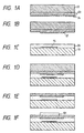
- Figs. 1A to 2K illustrate different steps of forming a microstructure in a mode of carrying out the method according to the invention
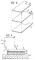
- Fig. 3 is a schematic perspective view of a microstructure prepared by this method.
- the microstructure shown comprises a first substrate 10 which is a glass substrate, a stationary (drive) electrode 15 and a fixed electrode 16 of thin film formed on the glass substrate 10, a movable electrode 17 of a p + Si layer provided with a torsion bar 11 and held on the upper surface of the torsion bar 11 by a pair of support members 13, 13' with a void interposed between itself and the substrate and a lever 12 of a patterned Si structure layer arranged on the movable electrode 17.
- the movable electrode and the lever constitute a beam 1.
- the support members 13, 13' are made of an electroconductive material such as aluminum to electrically connect the movable electrode 17 and the fixed electrode 16.
- the illustrated microstructure is an electrostatic actuator having a beam that can be displaced by applying a voltage to the drive electrode 15 and the fixed electrode 16, which is electrically connected to the movable electrode 17 provided at the lower surface of the beam.
- the movable electrode 17 is suspended by the support members 13, 13' from the upper surface of the torsion bar 11 with a void interposed between the electrode and the glass substrate, the support members 13, 13' mechanically and electrically connecting the beam and the glass substrate 10 and fixed electrode 16 by means of an air bridge structure.
- the torsion bar 11 is twisted to rotate and displace the lever toward the substrate as a voltage is applied to the drive electrode 15 and the movable electrode 17. Since the lever has a thickness greater than that of the torsion bar, it is not bent if a voltage is applied to the electrodes.
- the movable electrode of the beam of the electrostatic actuator having the above described configuration is disposed on the lower surface of the lever, the distance separating the movable electrode and the drive electrode is reduced by the thickness of the lever if compared with the case where the movable electrode is arranged on the upper surface of the beam and hence a relatively low drive voltage may be used to displace the beam.
- a microstructure having a configuration as shown in Fig. 3 was formed through the steps of Figs. 1A to 2K, illustrating the microstructure in cross section in different manufacturing steps.
- a p-type Si substrate 22 carrying thereon an n-type diffusion layer (80 ⁇ cm, thickness: 3 ⁇ m) for a structure layer 23 was used for the second substrate and boron ions were injected into the diffusion layer to form a p + layer 24 (120 ⁇ /square, thickness: 0.5 ⁇ m) (Fig. 1A).
- Photoresist was applied to the substrate and subjected to a patterning operation using a photolithography process, where the applied photoresist was exposed to light and photochemically developed.
- the p + layer 24 was etched by using the mask of the photoresist pattern and CF 4 gas in a reactive ion etching (RIE) process to produce a movable electrode 17.
- RIE reactive ion etching
- the photoresist was stripped off in a resist stripping solution to produce a second substrate carrying thereon a movable electrode (Fig. 1B).
- the movable electrode was part of a structure layer.
- a glass substrate 10 (#7059 Corning: tradename) carrying thereon a drive electrode 15 and a fixed electrode 16 was used for the first substrate.
- the glass substrate 10 has a thermal expansion coefficient greater than that of Si by about 1.4 times. More specifically, a Cr film and an Au film were successively formed on the glass substrate 10 by electron beam vapour deposition to thicknesses of 5nm and 200nm respectively and a photoresist layer was subjected to a patterning operation in a photolithography process. The obtained mask of photoresist was used to produce the drive electrode 15 and the fixed electrode 16 having profiles conforming to the pattern of photoresist as shown in Fig.
- the second substrate as shown in Fig. 1B and the first substrate carrying thereon an adhesive layer 26 as shown in Fig. 1C were pressed again each other from the rear sides. While the movable electrode 17 was buried in the adhesive layer 26 in this example, it may be kept unburied by controlling the pressure applied to the substrate when they are bonded together. After bonding the first substrate and the structure layer on the second substrate together with the adhesive layer disposed therebetween, the adhesive layer was heat set at 150°C.
- the bonded substrates of Fig. 1D was subjected to electrolytic etching at 80°C in a 30wt% KOH solution by applying a positive voltage of 3V to the diffusion layer relative to the natural electrode potential to remove the p-type Si substrate of the second substrate (Fig. 1E).
- the structure layer 23 of an n-type diffusion layer was not etched by the electrolytic etching.
- a pattern was formed on the structure layer 24 in a photolithography process, where photoresist was applied to the structure layer 24, exposed to light and photochemically developed for the pattern (Fig.
- the structure layer 23 was subjected to reactive ion etching (RIE), using the mask of photoresist 101 and CF 4 gas to produce a lever pattern 25 of the n-type Si diffusion layer. Then, the photoresist pattern 101 was removed and, simultaneously, the adhesive layer was etched to the pattern of the lever and the torsion bar by oxygen gas (Fig. 2G).
- RIE reactive ion etching
- an Al film 27 was formed on the lever and the movable electrode to a thickness of 1 ⁇ m for the support members by means of sputtering, a type of vacuum deposition, using an Al target (Fig. 2H).
- photoresist 102 was applied on the Al film, exposed to light and photochemically developed (Fig. 2I) and the Al film 27 was subjected to a patterning operation, using an Al etchant consisting of phosphoric acid, nitric acid and acetic acid to produce the pattern of the support member 13' on the torsion bar 11 (Fig. 2J).
- the photoresist 102 and the PMMA of the resin film under the movable electrode were etched out to produce a void 29 by oxygen plasma.
- an electrostatic actuator having a profile as shown in Fig. 3 was produced, the electrostatic actuator having a torsion bar type beam of bulk (crystalline) Si provided with a void 29 and supported by the Al film as shown in Fig. 2K.
- the electrodes of the electrostatic actuator were not etched out by oxygen plasma and the problem of sticking that may arise when the sacrificial layer is removed by wet etching was successfully avoided.
- the torsion bar type beam formed was free from internal stress and warping and was successfully prepared. The free end of the beam was displaced as the torsion bar was twisted to rotate when a voltage was applied to the movable electrode and the drive electrode.
- the first substrate and the structure layer on the second substrate could be bonded together at temperature as low as 150°C and materials having different thermal expansion coefficients could be selected for the substrates.
- the resin film plays the role of an adhesive for bonding the first substrate and the structure layer on the second substrate and, at the same time, that of a sacrificial layer for forming a microstructure.
- the adhesive layer was formed on the first substrate, which was then bonded with the structure layer on the second substrate in the above example, the adhesive layer may alternatively be arranged on the structure layer on the second substrate or an adhesive layer may be formed on both the first substrate and the structure layer on the second substrate to produce a beam.
- the movable electrode is formed with a p + layer and then the pattern of a lever is formed on the back side of the structure layer as viewed from the movable electrode. With this arrangement, they may be made to show respective profiles that are not affected by each other.
- an electrically insulated microstructure can be formed on the substrate by the same process if the Al thin film is replaced by a sacrificial layer of resin film formed by vacuum deposition and an insulating film such as silicon dioxide film formed at temperature that does not damage the adhesive layer.
- a glass substrate was used for the first substrate in the above example, it may be replaced by a substrate of an insulating material such as quartz, Al 2 O 3 , MgO or ZrO 2 , a semiconductor such as Si, GaAs or InP or a metal, using the same process.
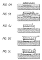
- Figs. 4A to 6P illustrate different steps of forming a microstructure in another mode of carrying out the method according to the invention
- Fig. 7 is a schematic perspective view of a microstructure prepared by the method
- Fig. 8 is an exploded view of the beam section of the microstructure, illustrating the multilayer structure of the beam, which beam 2 comprises a lever 32, a movable electrode 37 and a dummy electrode 39.
- the microstructure comprises a first substrate 30 which is an Si substrate, an insulation layer 34 of silicon dioxide film, a drive electrode 35 formed on the insulation layer 34 and a pair of fixed electrodes 38, 38' of thin film formed also on the insulation layer 34.
- the lever 32 is a cantilever of patterned silicon dioxide film and held at the upper surface thereof by a pair of support members 33, 33' of an electroconductive material with a void interposed therebetween.
- a movable electrode 37 and a dummy electrode 39 are arranged respectively on the lower surface and on the upper surface of the lever 32.
- the support member 33 electrically connects the dummy electrode 39 and the fixed electrode 38.
- the support member 33' electrically connects the movable electrode 37 and the fixed electrode 38' by way of a contact hole 36 formed in the lever 32 by means of a contact 31.
- the microstructure having a configuration as described above operates as a cantilever type electrostatic actuator that can be bent and deformed by applying a voltage to the drive electrode 35 and the fixed electrode 38' connected to the movable electrode 37 disposed on the lower surface of the lever 32 by way of the support member 33'.
- the beam 2 is suspended by the support members 33, 33' at the upper surface thereof with a void interposed therebetween and the support members 33, 33' mechanically and electrically connect the beam 32 onto the insulation layer 34 and the fixed electrodes 38, 38' to produce an air bridge structure.
- the beam is bent and deformed to displace the free end of the beam toward the substrate when a voltage is applied to the drive electrode 35 and the fixed electrode 38'.
- the distance between the movable electrode and the drive electrode can be reduced by the thickness of the beam if compared with a case where the movable electrode is arranged on the upper surface because the movable electrode is provided at the lower surface of the beam so that the voltage required to be applied to the electrodes in order to displace the beam can also be reduced.
- the dummy electrode arranged on the upper surface of the lever 32 effectively prevents the microstructure from being bent by the internal stress found within the lever 32 and the thin movable electrode 37 because of the vertically symmetrical arrangement of the dummy electrode and the movable electrode relative to the lever. In short, the dummy electrode operates to cancel any possible bend on the part of the lever.
- a microstructure as shown in Figs. 4A to 7 was prepared.
- Figs. 4A to 6P illustrate the microstructure in cross section taken along line 6P-6P of Fig. 7 in different manufacturing steps.
- an Si substrate 40 was thermally oxidized by using an oxidizing gas (a mixture gas of oxygen and hydrogen) to form a structure layer 43 of silicon dioxide having a thickness of 1 ⁇ m and then a sacrificial layer for pattern transfer 41 of Al film was formed by electron beam vapour deposition, which is a technique to form a thin film by deposition, to a thickness of 200nm (Fig. 4A) before the second substrate 42 of a glass substrate (#7740 Corning: tradename) and the sacrificial layer for pattern transfer 41 were bonded together by anode coupling (Fig. 4B).
- an oxidizing gas a mixture gas of oxygen and hydrogen
- reference numeral 63 denotes a power source for applying a voltage to the sacrificial layer for pattern transfer (Al film) formed on the Si substrate 40 having a structure layer 43 of silicon dioxide film and the second substrate 42 of glass substrate, said power source being connected to needle electrodes 61 and 65 by way of lead wires 62 and 64 respectively.
- Reference numeral 60 denotes a platen provided with a heater.
- the second substrate 42 was placed on the sacrificial layer for pattern transfer (Al film) 41 and a voltage of 500V was applied for 20 minutes from the power source 63 to the second substrate and the sacrificial layer for pattern transfer to bind them together, while maintaining the temperature of the platen to 300°C.
- the Si substrate 40 was removed by etching in a KOH 30wt% aqueous solution heated to 100°C to produce the second substrate carrying thereon the structure layer 43 and the sacrificial layer for pattern transfer (Fig. 4C).
- the structure layer of silicon dioxide film was not etched by wet etching using the alkaline aqueous solution because it is resistant against alkaline wet etching.
- an electroconductive thin film 201 was formed on the structure layer 43 for the movable electrode. This was done by successively forming a Cr film and an Au film to respective thicknesses of 5nm and 400nm by electron beam vapor deposition, patterning a photoresist layer 103 in a photolithography process (Fig. 4D) and then patterning the Cr and Au layers for the movable electrode respectively by means of an Au etchant, which was an aqueous solution of iodine and potassium iodide, and a Cr etchant, which was an aqueous solution of cerium ammonium nitrate and perchloric acid to make them show the profile of the movable electrode as shown in Fig.
- an Au etchant which was an aqueous solution of iodine and potassium iodide
- a Cr etchant which was an aqueous solution of cerium ammonium nitrate and perchloric acid to make them show the profile of the movable
- the insulation layer 34 is a silicon dioxide film formed by thermally oxidizing part of the Si substrate 30 to a thickness 1 ⁇ m by means of oxidizing gas.
- the drive electrode 35 and the fixed electrodes 38, 38' were prepared by forming electroconductive layers of an Cr film (5nm) and an Au film (100nm) and patterning them appropriately as in the case of preparing the movable electrode 37.
- an adhesive layer 46 was formed on the first substrate by applying resin with a spinner.
- the resin was a rubber type resist OMR-83 (tradename) available from Tokyo Ohka Co., Ltd. (Fig. 4F).
- the second substrate of Fig. 4E and the first substrate of Fig. 4F were pressed against each other from the rear sides thereof and heat treated at 150°C to heat set the resin of the adhesive layer and rigidly bind the substrates together as shown in Fig. 4G.
- the adhesive layer showed a thickness of 2 ⁇ m after the heat setting operation.
- the sacrificial layer for pattern transfer 41 was removed by an Al etchant containing phosphoric acid nitric acid and acetic acid and heated to 80°C to release the second substrate.
- the structure layer that had been patterned to show a beam-like profile and the movable electrode were transferred onto the adhesive layer of the first substrate.
- a dummy electrode 39 was prepared by forming a metal layer 202 of a Cr film (5nm) and an Au film (100nm), applying photoresist 104 thereto, patterning them appropriately in a photolithography process as in the case of preparing the drive electrode 35 and the fixed electrodes 38, 38' (Fig. 5I) and then etching the metal layer 202, using the mask of the photoresist 104 and Au and Cr etchant. Thereafter, the structure layer having the pattern of a lever was used as a mask in an operation of patterning the resin adhesive layer to produce there a pattern same as that of the lever pattern by RIE using oxygen gas.
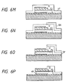
- photoresist 105 was applied to the structure layer having the lever pattern and subjected to a patterning operation in a photolithography process (Fig. 5K) and the patterned photoresist 105 was used as a mask to etch the structure layer by reactive ion etching (RIE) using CF 4 gas and produce a contact hole 36 (Fig. 5L). Thereafter, the photoresist 105 was removed by reactive ion etching (RIE) using oxygen gas. Then, an Al film 42 was formed to a thickness of 2 m for a support layer on the lever 32 of silicon dioxide prepared in a manner as described above and the movable electrode 37 under the contact hole 36 as well as on the dummy electrode 39 (Fig. 6M).
- RIE reactive ion etching
- Photoresist 106 was formed on the Al film and patterned in a photolithography process (Fig. 6N). Subsequently, the Al film 47 was patterned by means of an Al etchant containing phosphoric acid, nitric acid and acetic acid and heated to 50°C to produce support members 33, 33' (Fig. 60, where the support member 33 is not shown). With the above arrangement, the support member 33' electrically connected the movable electrode 37 and the fixed electrode 38' (not shown) by way of the contact hole, while the support member 33 electrically connected the dummy electrode 39 and the fixed electrode 38 (not shown).
- a microstructure that had a configuration as shown in Fig. 7 and comprised a 1 ⁇ m thick cantilever type beam 2 of silicon dioxide film carrying electrodes on the upper and lower surfaces and mechanically held by an Al film was produced with a void provided between the cantilever and the substrate.
- the movable electrode could be provided at the lower surface of the beam and electrically connected with a fixed electrode formed on the first substrate via a support member.
- a voltage of 20V was applied to the movable electrode and the drive electrode of the electrostatic actuator having a 100 ⁇ m long cantilever, the free end of the beam was displaced toward the first substrate by about 0.5 ⁇ m with the bending motion of the cantilever.
- the dummy electrode arranged on the upper surface of the beam effectively canceled any possible bent of the beam that could be produced by the internal stress of the movable electrode 37 under the lever 32.
- a cantilever type beam of silicon dioxide film that did not carry any movable electrode and dummy electrode was prepared to find out that no bending was observable on the part of the beam. While it is very difficult to eliminate the intrinsic stress generated in a thin silicon dioxide film during the process of preparing it by vacuum deposition, a silicon dioxide film produced by oxidizing bulk Si is amorphous and homogeneous and therefore it is not bent in the form of a monolayer. In this example, the Au layer was made as thick as 400nm, which was close to the thickness of the silicon dioxide film.
- an electrostatic actuator having a beam that was not provided with a dummy electrode in Fig. 7 was also prepared to find that the free end of the beam was bent away from the first substrate by more than 1 ⁇ m. This was because the Au film formed by vapor deposition for the movable electrode was subjected to compression stress.
- the beam of an electrostatic actuator according to the invention is bent upward, the distance between the movable electrode and the drive electrode is enlarged so that a higher voltage is required do drive the beam to move by a distance comparable to that of displacement of the beam of an electrostatic actuator without such bending.
- the beam of an electrostatic actuator with a movable electrode made of Ag and without a dummy electrode prepared for comparison was bent downward to reduce the distance between the first substrate and the free end of the beam and proved to be inoperative because of the reduced gap between the substrate and the beam.
- Fig. 60 showing a dummy electrode, it can be utilized to take out the tunnel current that may be generated between opposite surfaces of a specimen to be observed by arranging a probe of an electroconductive material on the dummy electrode according to the method proposed by Spindt (C. A. Spindt, et al., "Physical properties of film field emission cathode with molybdenum cones", J. Appl. Phys., 47 . 1976, pp. 5248-5263) so that an STM probe provided with an electrostatic actuator can be prepared by removing the photoresist 106 and the adhesive layer.
- Spindt C. A. Spindt, et al., "Physical properties of film field emission cathode with molybdenum cones", J. Appl. Phys., 47 . 1976, pp. 5248-5263
- the dummy electrode as a shield electrode for cutting off any external electric fields that can generate noise other than the noise produced by the electric field of the drive electrode by grounding the dummy electrode. While the structure layer of this example was provided with a single dummy electrode and a single movable electrode, it may alternatively be provided with more than one dummy electrode and more than one movable electrode .
- a structure layer is prepared after forming a movable electrode by means of a thin film deposition technique
- the pattern of the drive electrode is transferred to the structure layer also on the stepped areas of the pattern of the movable electrode.
- the pattern of the beam is formed on the structure layer after forming the movable electrode to be ultimately arranged on the structure layer vis-a-vis the first substrate, a beam can be formed from a flat structure layer regardless of the stepped areas of the pattern of the movable electrode.
- the structure layer carrying an electrode section is transferred onto the first substrate in a reversed manner, the electrode section can be formed vis-a-vis the first substrate.
- the first substrate can be provided with a very flat and smooth surface by applying resin thereto regardless of the undulations produced by the drive electrode and the fixed electrodes so that the substrates can be firmly bonded together as a very flat adhesive surface is prepared for them.
- a microstructure can be formed without problem if an Si substrate 30 carrying thereon integrated circuits is used for the first substrate. Since photoresist scarcely contains mobile ions, they hardly penetrate into electronic devices such as MOS transistors to interfere with the proper operation of such devices. While Si is used for the substrate, it may be replaced by a glass substrate or a substrate of some other material selected from GaAs, metals and metal film.
- a voltage of 100V may be applied to the Al of the sacrificial layer for pattern transfer 41 and the Si substrate of the first substrate to generate electrostatic force and the generated electrostatic force may be utilized to press the substrates against each other from the back sides in stead of applying physical pressure to the substrates from the rear side.
- Al film is used for the sacrificial layer for pattern transfer in the above description, Ti, Ni or some other metal that can be bonded by anode coupling may alternatively be used in combination with an etchant that does not corrode the resin film and the structure layer to produce a similar microstructure.
- any vapor of the solvent generated when the resin film is heat set in the step of Fig. 4G can be made to escape through the grooves. If no such grooves are formed, bubbles of the evaporated solvent produced in the heat setting process can be trapped between the adhesive layer and the structure layer unless the concentration of the solvent contained in the resin solution to be applied to the substrate is rigorously controlled. This problem is eliminated by providing grooves.
- the resin film operates as an adhesive layer for bonding the first substrate and the structure layer and, at the same time, takes the role of a sacrificial layer for forming a microstructure.
Description
- This invention relates to a microstructure to be prepared by means of micromechanical technologies and it also relates to a method of forming a microstrucuture by using a sacrificial layer.
- In recent years, studies have been made to produce minute machines comprising small one or more than one mechanisms by means of micromechanical technologies. In particular, such a microstructure realized by applying technologies developed for forming semiconductor integrated circuits (semiconductor photolithography process) can be used to produce a number of minute mechanical components on a common substrate on a highly reproducible basis. Thus, minute components can be prepared for minute machines at reduced cost and such minute components provide an enhanced responsiveness if compared with conventional mechanical structures.
- Three typical methods are popularly known for manufacturing a microstructure on a substrate. Firstly, there is a method for producing a microstructure such as a wobble micromotor of polysilicon film (M. Mehregany et al., "Operation of microfabricated harmonic and ordinary side-drive motors", Proceedings IEEE Micro Electro Mechanical Systems Workshop, 1990, pp. 1-8) or a linear microactuator (P. Cheung et al., "Modeling and position-detection of a polysilicon linear microactuator", Micromechanical Sensors, Actuators and Systems ASME 1991, DS C-Vol. 32, pp. 269-278), with which a sacrificial layer of silicon dioxide film and a thin silicon film of polysilicon, SOI (Si on Insulator) or SIMOX (Separation by ion implantation of oxygen) (B. Diem et al., "SOI (SIMOX) as a Substrate for Surface Micromachining of Single Crystalline Silicon and Actuators", The 7th International Conference on Solid-State Sensors and Actuators, transducers '93, June 7-10, 1993, pp. 233-236) formed to produce a microstructure are patterned to show a desired profile and subsequently the silicon dioxide film is used as a sacrificial layer and removed with an aqueous solution of fluorine.
- However, since this method involves the use of an aqueous solution of fluorine in order to etch out the silicon dioxide, a material that resists corrosion by fluoric acid has to be selected for the microstructure and hence such corrosive substances as aluminum cannot be used for the electrodes of the microstructure. Additionally, the polysilicon of the microstructure has to be controlled for its membrane stress in order to prevent it from warping. If an SOI substrate is used, the silicon dioxide supporting the microstructure can be etched back to consequently reduce the microstructure to show a beam-shaped profile and make it difficult to electrically connect the substrate and the structure when the silicon dioxide lying under the bulk Si thin film is removed.
- Secondly, there is a known a method of forming a spatial light modulator comprising a micromirror of an aluminum (Al) thin film (L. J. Hornbeck, Japanese Patent Application Laid-Open No. 2-8812) by applying photoresist onto a substrate to form a sacrificial layer, forming thereon an Al thin film, patterning the Al film to a desired profile and thereafter removing the photoresist by dry etching using oxygen plasma to produce a microstructure comprising an Al thin film.
- With this technique, it is possible to form a microstructure on a substrate selected from a variety of candidates because the sacrificial layer is made of photoresist, the use of which is not restricted by the surface coarseness of the substrate. Thus, the sacrificial layer can be removed by drying etching using the technology of reactive ion etching (RIE) and any possible sticking phenomenon that may appear between the microstructure and the substrate if a wet etching technique is used to remove the sacrificial layer can be successfully avoided. However, the process of forming the aluminum thin film for the structure has to be conducted at temperature that is low enough to prevent photoresist from being damaged by heat to impose rather rigorous restrictions on the selection of material for the microstructure. Additionally, since the microstructure is produced by means of a thin film forming technique such as vacuum deposition or sputtering, the membrane stress of the thin film has to be so controlled as to prevent the microstructure from being warped by the membrane stress.
- Thirdly, there is known a method of forming the pattern of a microstructure on a bulk Si substrate, coupling part of the pattern to the glass substrate by anode coupling and etching the coupled Si substrate from the rear surface in such a way that only the microstructure is left on the glass substrate. A linear actuator made of bulk Si thin film formed from an Si substrate (Y. Gianchandani et al., "Micro-Size High Aspect Ratio Bulk Silicon Micromechanical Devices", Proceedings IEEE Micro Electro Mechanical Systems Workshop, 1992, pp. 208-213) and a cantilever for an AFM (Atomic Force Microscope) made of silicon nitride film (T. A. Albrecht et al., United States Patent No. 5,221,415) can be prepared with this technique.
- Since this method does not involve the use of a sacrificial layer, a microstructure can be made of a material that may be corroded by fluoric acid. However, since it has to be coupled with glass by anode coupling, candidate materials are limited to electroconductive silicon that can be easily oxidized, metals such as Si, Al, Ti and Ni and silicon nitride or oxide that can be anode-coupled only in the form of a thin film formed on a Si substrate. Additionally, since the process of anode coupling has to be conducted at temperature higher than 300°C, the glass to be coupled with a microstructure is required to show a thermal expansion coefficient substantially equal to that of the Si substrate. Thus, glass that can be used with this method is limited to Pyrex glass (e.g., #7740 Corning: tradename). Additionally, since a void has to be formed in advance on the coupling surface, electrodes cannot be arranged on the microstructure after the coupling operation. Moreover, since the substrate has to be made of glass containing mobile ions, circuits cannot be formed on the substrate to a high degree of integration. Finally, since the surface coarseness of the glass and the electroconductive material has to be held to less than 50 nm (500 Å) for coupling the glass and the electroconductive material by anode coupling, they cannot be coupled on stepped wires.
- A method of manufacturing a microstructure is disclosed in EP-A-417523 which involves laminating layers forming a spacer, a hinge layer and beam layer on a substrate and then conducting patterning removal of these layers. When patterning the layer forming the spacer, only part of the spacer layer is removed, with the remaining portion acting as a support for a hinge layer and the beam layer.
- Another method of manufacturing a microstructure is disclosed in EP-A-0534406. A microstructure is prepared by patterning a supporting portion on the substrate followed by further patterning other substrates to form the microstructure.
- In view of the above identified problems, it is therefore an object of the present invention to provide a microstructure:
- (1) that is free from restrictions on the material of the microstructure and that of its substrate; and
- (2) allows electric connection between the microstructure having an electrode pattern and its substrate as well as a method for forming such a microstructure.
-
- In accordance with an aspect of the present invention there is provided a method of manufacturing a microstructure comprising:
- a first substrate;
- a beam member having a movable electrode provided on the surface of said beam member closer to said first substrate; and
- supporting means arranged to support said beam
member over said first substrate so that said movable
electrode is separated from said first substrate by an
air space, said method comprising steps of:
- (a) forming a structure layer, for forming the beam member, on a second substrate;
- (b) forming a movable electrode on said structure layer;
- (c) forming a beam member from said structure layer by removing part of said structure layer;
- (d) forming an adhesive layer on a surface of said first substrate and/or said second substrate;
- (e) joining said first substrate and said movable electrode via said adhesive layer;
- (f) removing said second substrate;
- (g) removing the part of said adhesive layer not sandwiched between said movable electrode and said first substrate;
- (h) forming a supporting means, said supporting means being attached to the surface of said first substrate and the surface of said movable electrode further from said first substrate; and
- (i) removing the remaining part of said adhesive layer so that said movable electrode is separated from the surface of said first substrate (10:30,34) by an air space (27;49).
-
- It is acknowledged with reference to Article 54(3) EPC that prior European Patent Application EP-A-0665590 discloses a method of manufacturing a similar microstructure to that above except in that the movable electrode is instead provided at the upper surface of the beam further from the substrate and the supporting means is attached to the beam member not only to the movable electrode itself.
- With the method of the present invention, the microstructure can be formed by a process to be conducted at relatively low temperature so that a substrate having a thermal expansion coefficient largely differing from that of the material of the remainder of the microstructure may be used.
- With the method of forming a microstructure according to the invention, the pattern of the stationary electrode and that of the structure layer may be formed, disregarding each other.
- Further, since the movable electrode can be finally placed opposite to the substrate after the formation of the structure layer, it is possible to form a beam of a flat structure layer regardless of steps that may be found on the pattern of the movable electrode.
-
- Figs. 1A to 1F are schematic illustrations showing steps of forming a microstructure in a mode of carrying out the method according to the invention.
- Figs. 2G to 2K are schematic illustrations showing steps to be followed after those of Figs. 1A to 1F.
- Fig. 3 is a schematic perspective view of an electrostatic actuator prepared by the method of forming a microstructure according to the invention.
- Figs. 4A to 4G are schematic illustrations showing steps of forming a microstructure in another mode of carrying out the method according to the invention.
- Figs. 5H to 5L are schematic illustrations showing steps to be followed after those of Figs. 4A to 4G.
- Figs. 6M to 6P are schematic illustrations showing steps to be followed after those of Figs. 5H to 5L.
- Fig. 7 is a schematic perspective view of an electrostatic actuator prepared by the method of forming a microstructure according to the invention.
- Fig. 8 is an exploded schematic view of the beam section of an electrostatic actuator prepared by the method of forming a microstructure according to the invention, illustrating the multilayer structure of the beam.
- Fig. 9 is a schematic sectional view of an electrostatic actuator prepared by the method of forming a microstructure according to the invention, illustrating the step of forming a silicon dioxide film for a structure layer on the second substrate with a sacrificial layer for pattern transfer interposed therebetween.
-
- Now, the present invention will be described by referring to the accompanying drawings that illustrate preferred embodiments of the invention.
- A known appropriate method can be used for forming an adhesive layer. For instance, a resin material may be diluted in an organic solvent and applied onto a substrate by means of a spinner, dipping or spraying technique to produce a resin film. With such an application technique, a flat resin film having a planar surface can be formed on the substrate, if it has a rough surface at the beginning, by which it is possible to join the surface and that of the other substrate without depending on the roughness of the surface. When a resin film is formed on an Si substrate carrying thereon integrated circuits, photoresist containing little impurities such as sodium ions may preferably be used for the resin film. Another material that may preferably used for the resin film is rubber type photoresist containing rubber that is highly adhesive and mechanically strong.
- For the purpose of the present invention, rubber as described in "Micromachining and Resist" (Saburo Nonogaki, ed. Japan Polymer Society, Kyoritu Publishing Co., Ltd., 1990, 1. 3, p. 11) may preferably used for rubber type resist. High resolution negative type photoresist available from Tokyo Ohka Kogyo Co., Ltd and containing rubber such as OMR-83 may also preferably be used for the purpose of the invention.
- A substrate carrying thereon the pattern of a structure formed by a combination of a semiconductor photolithography process and an etching process, a substrate carrying thereon a structure layer of thin film formed on a second substrate or a second substrate carrying thereon a structure layer with a sacrificial layer for pattern transfer interposed therebetween may suitably be used for the second substrate with a structure layer formed thereon.
- If a substrate carrying thereon the pattern of a structure formed by a combination of a semiconductor photolithography process and an etching process or a substrate carrying thereon a structure layer of thin film formed on a second substrate is selected, the substrate is thinned from the rear side until the structure layer is left there in the step of removing the second substrate by means of wet etching using an etching solution suitably selected for the substrate, dry etching using reactive gas or a technique of lapping the substrate with polishing granules. For instance, if the second substrate is made of Si, an alkaline aqueous solution such as a potassium hydroxide solution (KOH) or a tetramethyl ammonium hydroxide solution or an aqueous solution of a mixture of fluoric acid and nitric acid may preferably be used for the etching solution and a plasma gas containing CF4, SF6 or NF3 may preferably be used for the reactive gas. If an Si wafer having a pn junction is used for the structure, which is of the n-type, and the second substrate, which is of the p-type, only the structure of the n-type can be left unaffected by applying a voltage to the structure layer in an etching operation using an alkaline aqueous solution (B. Kloeck, et al., "Study of Electrochemical Etch-Stop for High-Precision Thickness Control of Silicon Membranes" IEEE TRANSACTIONS ON ELECTRON DEVICES, VOL. 36, NO. 4, pp. 663-669, 1989). If an Si bulk on which the pattern of a structure is formed by etching is used for the second substrate, the produced microstructure will be free from warping so that the problem of warping given rise to by the membrane stress in the process of forming a microstructure by forming a thin film on a sacrificial layer can be effectively eliminated.
- For a second substrate carrying thereon a structure layer with a sacrificial layer for pattern transfer interposed therebetween, a substrate prepared by using a glass substrate for the second substrate, forming a metal thin film as a sacrificial layer for pattern transfer and thereafter applying a voltage to the metal thin film and the glass substrate to produce a junctioned body coupled by anode coupling, a substrate having a sacrificial layer for pattern transfer of silicon dioxide and an intermediary layer of an SOI or SIMOX substrate carrying thereon a structure layer of silicon film or a junctioned body realized by forming a sacrificial layer for pattern transfer and a structure layer of thin film on the second substrate may appropriately be used. For the sacrificial layer for pattern transfer, a material that can be removed by an etchant that, however, does not corrode at least the adhesive layer and the structure layer may suitably be selected. A thin film deposition technique such as vapor deposition or CVD (chemical vapor deposition) may suitably be used for forming a thin film. If the technique of anode coupling is used, the second substrate may be a glass substrate containing mobile ion of an alkali metal (e.g. sodium) whereas the metal film may be made of a metal good for anode coupling such as Si, Al, Ti or Ni or an alloy containing any of such metals. If such a metal film is to be formed on the structure layer, a material selected from various different substances including insulators, semiconductors and metals may be bonded onto a glass substrate by anode coupling.
- If the microstructure has a thickness less than tens of several µm (micrometers), it provides a handling problem when junctioning the microstructure onto the second substrate. If such is the case, the structure layer has to be thinned to reduce its thickness after junctioning it to the second substrate. Alternatively, a substrate on which a structure layer is formed in advance may be used so that the structure layer may be left when the substrate is removed by some means. For reducing the thickness of or totally removing the substrate, a technique is selected from wet etching using an etching solution suited for the substrate, dry etching using reactive gas, lapping using grinding granules and polishing and the substrate is thinned from the rear side so that the structure layer having a desired thickness may be junctioned onto the substrate. If a bulk substrate of Si or GaAs is used, a microstructure produced as a final product of the thinned bulk is free from warping so that the problem of warping given rise to by the membrane stress in the process of forming a microstructure by forming a thin film on a sacrificial layer can be effectively eliminated. Additionally, the thickness of the junctioned layers can be appropriately regulated as they are made very thin.
- In the step of forming an electrode section on the microstructure, it is produced either by forming a thin film of electroconductive body by vacuum deposition on the structure layer that has been formed on the second substrate and subsequently forming its pattern on the thin film of electroconductive body by semiconductor photolithography or by arranging a structure layer that carries thereon an electroconductive layer on the second substrate and subsequently forming its pattern on the electroconductive layer. The electroconductive layer may be a p+ layer formed on an Si substrate.
- In the step of joining the first substrate and the structure layer and electrode section, the first substrate is pressed against the second substrate from the rear side and then the organic solvent contained in the resin film of the adhesive layer is made to evaporate by heating the layer until the resin is heat set and consequently the force binding the substrates is increased. If the first and second substrates are electroconductive, they may be joined together by applying a voltage to each of them to generate electrostatic force there, which force is then utilized to press them against each other. When this joining step is over, the electrode section is located between the adhesive layer and structure layer.
- The vapour of the organic solvent generated during the heat treatment of the adhesive layer can be made to escape to the ambient air by forming a groove on the first substrate and/or the structure layer. Any stepped portions of the pattern of the structure layer formed by semiconductor photolithography may be utilized for such grooves.
- The operation of heat setting the resin film of the adhesive layer may be conducted at relatively low temperature to avoid damaging the first and second substrate because of the difference of their thermal expansion coefficients so that the first substrate may be selected appropriately without considering the difference.
- In the step of removing the second substrate, the second substrate and the structure layer are separated from each other without separating the adhesive layer on the first substrate and the structure layer if the second substrate carries thereon a sacrificial layer for pattern transfer and the latter is removed. In other words, the structure on the second substrate is transferred onto the adhesive layer of the first substrate as a result of this step.
- The support layer is designed to mechanically connect the first substrate and the structure layer and/or electrode section and suspend the transferred structure layer and/or electrode section from above as it is formed before removing the adhesive layer. If a metal thin film (e.g., aluminum) is used for the support layer, the structure layer and/or electrode section and the first substrate will also be connected electrically.
- In the step of removing the adhesive layer of resin film, it is eliminated by wet etching, with which the resin film is dipped into a solution that dissolves the film, or by drying etching, with which the layer is ashed by oxygen plasma. Dry etching is advantageous in that it can avoid the problem of sticking that arises when the sacrificial layer is removed by wet etching.
- A microstructure produced through the above steps comprises a first substrate, a support section or a support layer and a beam comprising a structure layer and an electrode, of which the beam is supported by the support section from the upper surface of the beam through a void between the beam and the substrate, the electrode being disposed on the lower surface of the beam. Then, a fixed electrode and a stationary (drive) electrode are arranged on the first substrate and the structure layer is processed by patterning to produce a cantilever type or torsion beam type beam so that the electrode on the beam may become movable. With such an arrangement, the movable electrode and the fixed electrode are electrically connected by the support section and, at the same time, the beam and the movable electrode are mechanically supported by it from the upper surface of the beam to produce an electrostatic actuator where the position of the beam can be changed by applying a drive voltage to the drive electrode and the movable electrode. A microstructure manufactured by the method of the present invention may be an electrostatic actuator, a cantilever to be used for a microscope system such as an AFM or an STM (scanning tunneling microscope) for a detecting tunneling current, van der Waals force, magnetic force, electrostatic force or the like or a wiring system having an air bridge structure. In the case of an electrostatic actuator having the above described configuraiton, since the movable electrode is provided at the lower surface of the beam below the structure layer part of the beam, the distance separating the movable electrode and the stationary electrode is reduced by the thickness of the structure layer as compared with a movable electrode arranged on the upper surface of the structure layer and, therefore, a relatively low drive voltage may be used to displace the beam. If the structure layer part of the beam is made as thin as the movable electrode, the risk of warping of the beam that may appear due to the internal stress can be eliminated by arranging another electrode on the upper surface of the structure layer to produce a symmetrical structure.
- According to the method just mentioned, the structure layer formed on the second substrate and electrode section formed on the structure layer and the first substrate are joined together with the adhesive layer of resin film formed on both or either of the first and second substrates and, thereafter, the second substrate is removed. The use of resin film for the adhesive layer allows the materials of the first substrate, the second substrate and the structure layer formed on the second substrate to be selected from a wide range of candidates and also the movable electrode to be formed on the structure layer before removing the resin film. Additionally, the adhesive layer can be removed by means of a solvent, ashing or heating if it is made of resin film so that the electrode section does not need to be subjected to an etching operation. Finally, the problem of sticking that arises when the sacrificial layer is removed by wet etching can be effectively avoided by dry etching the adhesive layer of resin film.
- Now, the method of forming a microstructure according to the invention and a microstructure prepared by such a method will be described by way of examples, referring to Figs. 1A through 9 of the accompanying drawings.
- Figs. 1A to 2K illustrate different steps of forming a microstructure in a mode of carrying out the method according to the invention and Fig. 3 is a schematic perspective view of a microstructure prepared by this method. Referring to Fig. 3, the microstructure shown comprises a
first substrate 10 which is a glass substrate, a stationary (drive)electrode 15 and a fixedelectrode 16 of thin film formed on theglass substrate 10, amovable electrode 17 of a p+ Si layer provided with atorsion bar 11 and held on the upper surface of thetorsion bar 11 by a pair ofsupport members 13, 13' with a void interposed between itself and the substrate and alever 12 of a patterned Si structure layer arranged on themovable electrode 17. The movable electrode and the lever constitute abeam 1. Thesupport members 13, 13' are made of an electroconductive material such as aluminum to electrically connect themovable electrode 17 and the fixedelectrode 16. The illustrated microstructure is an electrostatic actuator having a beam that can be displaced by applying a voltage to thedrive electrode 15 and the fixedelectrode 16, which is electrically connected to themovable electrode 17 provided at the lower surface of the beam. With such an arrangement, themovable electrode 17 is suspended by thesupport members 13, 13' from the upper surface of thetorsion bar 11 with a void interposed between the electrode and the glass substrate, thesupport members 13, 13' mechanically and electrically connecting the beam and theglass substrate 10 and fixedelectrode 16 by means of an air bridge structure. Thetorsion bar 11 is twisted to rotate and displace the lever toward the substrate as a voltage is applied to thedrive electrode 15 and themovable electrode 17. Since the lever has a thickness greater than that of the torsion bar, it is not bent if a voltage is applied to the electrodes. - Since the movable electrode of the beam of the electrostatic actuator having the above described configuration is disposed on the lower surface of the lever, the distance separating the movable electrode and the drive electrode is reduced by the thickness of the lever if compared with the case where the movable electrode is arranged on the upper surface of the beam and hence a relatively low drive voltage may be used to displace the beam.
- In this example, a microstructure having a configuration as shown in Fig. 3 was formed through the steps of Figs. 1A to 2K, illustrating the microstructure in cross section in different manufacturing steps. A p-
type Si substrate 22 carrying thereon an n-type diffusion layer (80 Ω·cm, thickness: 3 µm) for astructure layer 23 was used for the second substrate and boron ions were injected into the diffusion layer to form a p+ layer 24 (120 Ω/square, thickness: 0.5 µm) (Fig. 1A). Photoresist was applied to the substrate and subjected to a patterning operation using a photolithography process, where the applied photoresist was exposed to light and photochemically developed. Then, the p+ layer 24 was etched by using the mask of the photoresist pattern and CF4 gas in a reactive ion etching (RIE) process to produce amovable electrode 17. Subsequently, the photoresist was stripped off in a resist stripping solution to produce a second substrate carrying thereon a movable electrode (Fig. 1B). In other words, the movable electrode was part of a structure layer. - A glass substrate 10 (#7059 Corning: tradename) carrying thereon a
drive electrode 15 and a fixedelectrode 16 was used for the first substrate. Theglass substrate 10 has a thermal expansion coefficient greater than that of Si by about 1.4 times. More specifically, a Cr film and an Au film were successively formed on theglass substrate 10 by electron beam vapour deposition to thicknesses of 5nm and 200nm respectively and a photoresist layer was subjected to a patterning operation in a photolithography process. The obtained mask of photoresist was used to produce thedrive electrode 15 and the fixedelectrode 16 having profiles conforming to the pattern of photoresist as shown in Fig. 3 by etching that used an Au etchant consisting of an aqueous solution of iodine and potassium iodide and a Cr etchant consisting of an aqueous solution of cerium ammonium nitrate and perchloric acid. Subsequently, a solution prepared by dissolving methyl polymethacrylate (PMMA) into methyl ethyl ketone (MEK) was applied to theglass substrate 10 with a spinner and preliminarily heated at 50°C for ten minutes to produce anadhesive layer 26 made of PMMA and having a thickness of 2.5 µm (Fig. 1C). Care should be needed to accurately control the amount of the solvent in the solution dissolving the resin to be applied because bubbles of vapour of the solvent might be trapped between the adhesive layer and the structure layer on the second substrate during the heating process. The preliminary heating operation was conducted at temperature sufficiently low to prevent the adhesive from being heat set, paying attention to eliminate any bubbles of the evaporated solvent remaining on the interface by accurately controlling the solvent contained in the resin film. When PMMA was used, the generation of bubbles could be completely suppressed by preliminarily heating the adhesive at 50°C for 10 minutes. - Then, the second substrate as shown in Fig. 1B and the first substrate carrying thereon an
adhesive layer 26 as shown in Fig. 1C were pressed again each other from the rear sides. While themovable electrode 17 was buried in theadhesive layer 26 in this example, it may be kept unburied by controlling the pressure applied to the substrate when they are bonded together. After bonding the first substrate and the structure layer on the second substrate together with the adhesive layer disposed therebetween, the adhesive layer was heat set at 150°C. - Subsequently, the bonded substrates of Fig. 1D was subjected to electrolytic etching at 80°C in a 30wt% KOH solution by applying a positive voltage of 3V to the diffusion layer relative to the natural electrode potential to remove the p-type Si substrate of the second substrate (Fig. 1E). Note that the
structure layer 23 of an n-type diffusion layer was not etched by the electrolytic etching. Thereafter, a pattern was formed on the structure layer 24 in a photolithography process, where photoresist was applied to the structure layer 24, exposed to light and photochemically developed for the pattern (Fig. 1F) and then thestructure layer 23 was subjected to reactive ion etching (RIE), using the mask ofphotoresist 101 and CF4 gas to produce alever pattern 25 of the n-type Si diffusion layer. Then, thephotoresist pattern 101 was removed and, simultaneously, the adhesive layer was etched to the pattern of the lever and the torsion bar by oxygen gas (Fig. 2G). - Thereafter, an
Al film 27 was formed on the lever and the movable electrode to a thickness of 1 µm for the support members by means of sputtering, a type of vacuum deposition, using an Al target (Fig. 2H). Then,photoresist 102 was applied on the Al film, exposed to light and photochemically developed (Fig. 2I) and theAl film 27 was subjected to a patterning operation, using an Al etchant consisting of phosphoric acid, nitric acid and acetic acid to produce the pattern of the support member 13' on the torsion bar 11 (Fig. 2J). Finally, thephotoresist 102 and the PMMA of the resin film under the movable electrode were etched out to produce a void 29 by oxygen plasma. Thus, an electrostatic actuator having a profile as shown in Fig. 3 was produced, the electrostatic actuator having a torsion bar type beam of bulk (crystalline) Si provided with a void 29 and supported by the Al film as shown in Fig. 2K. The electrodes of the electrostatic actuator were not etched out by oxygen plasma and the problem of sticking that may arise when the sacrificial layer is removed by wet etching was successfully avoided. - In the method just described, since the microstructure comprising the movable electrode and the lever was formed from a bulk (crystalline) Si substrate, the torsion bar type beam formed was free from internal stress and warping and was successfully prepared. The free end of the beam was displaced as the torsion bar was twisted to rotate when a voltage was applied to the movable electrode and the drive electrode.
- Because resin film was used for the adhesive layer, the first substrate and the structure layer on the second substrate could be bonded together at temperature as low as 150°C and materials having different thermal expansion coefficients could be selected for the substrates. As described earlier, for the purpose of the invention, the resin film plays the role of an adhesive for bonding the first substrate and the structure layer on the second substrate and, at the same time, that of a sacrificial layer for forming a microstructure.
- By applying resin film on the first substrate, it was made possible to smooth out the surface of the substrate that had been undulated by the components arranged there including the drive electrode and the movable electrode in order to produce a smooth bonding surface and achieve a good bonding effect for the substrates. While the adhesive layer was formed on the first substrate, which was then bonded with the structure layer on the second substrate in the above example, the adhesive layer may alternatively be arranged on the structure layer on the second substrate or an adhesive layer may be formed on both the first substrate and the structure layer on the second substrate to produce a beam.
- As described above, the movable electrode is formed with a p+ layer and then the pattern of a lever is formed on the back side of the structure layer as viewed from the movable electrode. With this arrangement, they may be made to show respective profiles that are not affected by each other.
- While an Al thin film was formed for the support members in the above example, it may be appreciated that an electrically insulated microstructure can be formed on the substrate by the same process if the Al thin film is replaced by a sacrificial layer of resin film formed by vacuum deposition and an insulating film such as silicon dioxide film formed at temperature that does not damage the adhesive layer. Similarly, while a glass substrate was used for the first substrate in the above example, it may be replaced by a substrate of an insulating material such as quartz, Al2O3, MgO or ZrO2, a semiconductor such as Si, GaAs or InP or a metal, using the same process.
- Figs. 4A to 6P illustrate different steps of forming a microstructure in another mode of carrying out the method according to the invention and Fig. 7 is a schematic perspective view of a microstructure prepared by the method. Fig. 8 is an exploded view of the beam section of the microstructure, illustrating the multilayer structure of the beam, which
beam 2 comprises alever 32, amovable electrode 37 and adummy electrode 39. As seen from Figs. 7 and 8, the microstructure comprises afirst substrate 30 which is an Si substrate, aninsulation layer 34 of silicon dioxide film, adrive electrode 35 formed on theinsulation layer 34 and a pair of fixedelectrodes 38, 38' of thin film formed also on theinsulation layer 34. Thelever 32 is a cantilever of patterned silicon dioxide film and held at the upper surface thereof by a pair ofsupport members 33, 33' of an electroconductive material with a void interposed therebetween. Amovable electrode 37 and adummy electrode 39 are arranged respectively on the lower surface and on the upper surface of thelever 32. Thesupport member 33 electrically connects thedummy electrode 39 and the fixedelectrode 38. The support member 33' electrically connects themovable electrode 37 and the fixed electrode 38' by way of acontact hole 36 formed in thelever 32 by means of acontact 31. The microstructure having a configuration as described above operates as a cantilever type electrostatic actuator that can be bent and deformed by applying a voltage to thedrive electrode 35 and the fixed electrode 38' connected to themovable electrode 37 disposed on the lower surface of thelever 32 by way of the support member 33'. - In the electrostatic actuator, the
beam 2 is suspended by thesupport members 33, 33' at the upper surface thereof with a void interposed therebetween and thesupport members 33, 33' mechanically and electrically connect thebeam 32 onto theinsulation layer 34 and the fixedelectrodes 38, 38' to produce an air bridge structure. The beam is bent and deformed to displace the free end of the beam toward the substrate when a voltage is applied to thedrive electrode 35 and the fixed electrode 38'. - With an electrostatic actuator having a configuration as described above, the distance between the movable electrode and the drive electrode can be reduced by the thickness of the beam if compared with a case where the movable electrode is arranged on the upper surface because the movable electrode is provided at the lower surface of the beam so that the voltage required to be applied to the electrodes in order to displace the beam can also be reduced. Additionally, the dummy electrode arranged on the upper surface of the
lever 32 effectively prevents the microstructure from being bent by the internal stress found within thelever 32 and the thinmovable electrode 37 because of the vertically symmetrical arrangement of the dummy electrode and the movable electrode relative to the lever. In short, the dummy electrode operates to cancel any possible bend on the part of the lever. - In an experiment, a microstructure as shown in Figs. 4A to 7 was prepared. Figs. 4A to 6P illustrate the microstructure in cross section taken along
line 6P-6P of Fig. 7 in different manufacturing steps. - In order to form a second substrate provided with a structure layer, an
Si substrate 40 was thermally oxidized by using an oxidizing gas (a mixture gas of oxygen and hydrogen) to form astructure layer 43 of silicon dioxide having a thickness of 1 µm and then a sacrificial layer forpattern transfer 41 of Al film was formed by electron beam vapour deposition, which is a technique to form a thin film by deposition, to a thickness of 200nm (Fig. 4A) before thesecond substrate 42 of a glass substrate (#7740 Corning: tradename) and the sacrificial layer forpattern transfer 41 were bonded together by anode coupling (Fig. 4B). - The process of anode coupling will now be described by referring to Fig. 9. In Fig. 9,
reference numeral 63 denotes a power source for applying a voltage to the sacrificial layer for pattern transfer (Al film) formed on theSi substrate 40 having astructure layer 43 of silicon dioxide film and thesecond substrate 42 of glass substrate, said power source being connected toneedle electrodes lead wires Reference numeral 60 denotes a platen provided with a heater. Thesecond substrate 42 was placed on the sacrificial layer for pattern transfer (Al film) 41 and a voltage of 500V was applied for 20 minutes from thepower source 63 to the second substrate and the sacrificial layer for pattern transfer to bind them together, while maintaining the temperature of the platen to 300°C. - Thereafter, the
Si substrate 40 was removed by etching in a KOH 30wt% aqueous solution heated to 100°C to produce the second substrate carrying thereon thestructure layer 43 and the sacrificial layer for pattern transfer (Fig. 4C). The structure layer of silicon dioxide film was not etched by wet etching using the alkaline aqueous solution because it is resistant against alkaline wet etching. - Subsequently, an electroconductive
thin film 201 was formed on thestructure layer 43 for the movable electrode. This was done by successively forming a Cr film and an Au film to respective thicknesses of 5nm and 400nm by electron beam vapor deposition, patterning aphotoresist layer 103 in a photolithography process (Fig. 4D) and then patterning the Cr and Au layers for the movable electrode respectively by means of an Au etchant, which was an aqueous solution of iodine and potassium iodide, and a Cr etchant, which was an aqueous solution of cerium ammonium nitrate and perchloric acid to make them show the profile of the movable electrode as shown in Fig. 8, using the mask ofphotoresist 103. Thephotoresist 103 was then removed by means of a resist stripping solution. Additionally, photoresist was applied anew to thestructure layer 43 and then patterned to the profile of a lever without a contact hole by photolithography and then thestructure layer 43 was subjected to a reactive ion etching (RIE) operation to produce the pattern of thelever 43 without a contact hole by using the mask of photoresist and CF4 gas. The photoresist was then stripped off by means of a resist stripping solution (Fig. 4E). - An
Si substrate 30 carrying thereon aninsulation layer 34, adrive electrode 35 and a pair of fixedelectrodes 38, 38' (not shown) was used for the first substrate. Theinsulation layer 34 is a silicon dioxide film formed by thermally oxidizing part of theSi substrate 30 to a thickness 1µm by means of oxidizing gas. Thedrive electrode 35 and the fixedelectrodes 38, 38' were prepared by forming electroconductive layers of an Cr film (5nm) and an Au film (100nm) and patterning them appropriately as in the case of preparing themovable electrode 37. Then, anadhesive layer 46 was formed on the first substrate by applying resin with a spinner. The resin was a rubber type resist OMR-83 (tradename) available from Tokyo Ohka Co., Ltd. (Fig. 4F). - After forming the
adhesive layer 46, the second substrate of Fig. 4E and the first substrate of Fig. 4F were pressed against each other from the rear sides thereof and heat treated at 150°C to heat set the resin of the adhesive layer and rigidly bind the substrates together as shown in Fig. 4G. The adhesive layer showed a thickness of 2µm after the heat setting operation. - Thereafter, the sacrificial layer for
pattern transfer 41 was removed by an Al etchant containing phosphoric acid nitric acid and acetic acid and heated to 80°C to release the second substrate. As a result, the structure layer that had been patterned to show a beam-like profile and the movable electrode were transferred onto the adhesive layer of the first substrate. - Subsequently, a
dummy electrode 39 was prepared by forming ametal layer 202 of a Cr film (5nm) and an Au film (100nm), applyingphotoresist 104 thereto, patterning them appropriately in a photolithography process as in the case of preparing thedrive electrode 35 and the fixedelectrodes 38, 38' (Fig. 5I) and then etching themetal layer 202, using the mask of thephotoresist 104 and Au and Cr etchant. Thereafter, the structure layer having the pattern of a lever was used as a mask in an operation of patterning the resin adhesive layer to produce there a pattern same as that of the lever pattern by RIE using oxygen gas. - Then,
photoresist 105 was applied to the structure layer having the lever pattern and subjected to a patterning operation in a photolithography process (Fig. 5K) and the patternedphotoresist 105 was used as a mask to etch the structure layer by reactive ion etching (RIE) using CF4 gas and produce a contact hole 36 (Fig. 5L). Thereafter, thephotoresist 105 was removed by reactive ion etching (RIE) using oxygen gas. Then, anAl film 42 was formed to a thickness of 2 m for a support layer on thelever 32 of silicon dioxide prepared in a manner as described above and themovable electrode 37 under thecontact hole 36 as well as on the dummy electrode 39 (Fig. 6M).Photoresist 106 was formed on the Al film and patterned in a photolithography process (Fig. 6N). Subsequently, theAl film 47 was patterned by means of an Al etchant containing phosphoric acid, nitric acid and acetic acid and heated to 50°C to producesupport members 33, 33' (Fig. 60, where thesupport member 33 is not shown). With the above arrangement, the support member 33' electrically connected themovable electrode 37 and the fixed electrode 38' (not shown) by way of the contact hole, while thesupport member 33 electrically connected thedummy electrode 39 and the fixed electrode 38 (not shown). - Finally, the
photoresist 106 and the adhesive layer of resin under the movable electrode were etched out by oxygen plasma to produce a void 49 (Fig. 6P). Thus, a microstructure that had a configuration as shown in Fig. 7 and comprised a 1 µm thickcantilever type beam 2 of silicon dioxide film carrying electrodes on the upper and lower surfaces and mechanically held by an Al film was produced with a void provided between the cantilever and the substrate. With the above method, the beam, the support members and the electrodes were left intact during the etching operation using oxygen plasma and the problem of sticking that may arise when the sacrificial layer is removed by wet etching was successfully avoided. - With the above method again, the movable electrode could be provided at the lower surface of the beam and electrically connected with a fixed electrode formed on the first substrate via a support member. When a voltage of 20V was applied to the movable electrode and the drive electrode of the electrostatic actuator having a 100 µm long cantilever, the free end of the beam was displaced toward the first substrate by about 0.5 µm with the bending motion of the cantilever.
- The dummy electrode arranged on the upper surface of the beam effectively canceled any possible bent of the beam that could be produced by the internal stress of the
movable electrode 37 under thelever 32. For the purpose of comparison, a cantilever type beam of silicon dioxide film that did not carry any movable electrode and dummy electrode was prepared to find out that no bending was observable on the part of the beam. While it is very difficult to eliminate the intrinsic stress generated in a thin silicon dioxide film during the process of preparing it by vacuum deposition, a silicon dioxide film produced by oxidizing bulk Si is amorphous and homogeneous and therefore it is not bent in the form of a monolayer. In this example, the Au layer was made as thick as 400nm, which was close to the thickness of the silicon dioxide film. For the purpose of comparison, an electrostatic actuator having a beam that was not provided with a dummy electrode in Fig. 7 was also prepared to find that the free end of the beam was bent away from the first substrate by more than 1 µm. This was because the Au film formed by vapor deposition for the movable electrode was subjected to compression stress. When the beam of an electrostatic actuator according to the invention is bent upward, the distance between the movable electrode and the drive electrode is enlarged so that a higher voltage is required do drive the beam to move by a distance comparable to that of displacement of the beam of an electrostatic actuator without such bending. The beam of an electrostatic actuator with a movable electrode made of Ag and without a dummy electrode prepared for comparison was bent downward to reduce the distance between the first substrate and the free end of the beam and proved to be inoperative because of the reduced gap between the substrate and the beam. Thus, any possible bending of the lever of an electrostatic actuator according to the invention that is attributable to the fact that the lever is made as thin as the movable electrode section can be effectively canceled by arranging a dummy electrode section on the upper surface of the lever to ensure vertical symmetry for the lever. - Referring to Fig. 60 showing a dummy electrode, it can be utilized to take out the tunnel current that may be generated between opposite surfaces of a specimen to be observed by arranging a probe of an electroconductive material on the dummy electrode according to the method proposed by Spindt (C. A. Spindt, et al., "Physical properties of film field emission cathode with molybdenum cones", J. Appl. Phys., 47. 1976, pp. 5248-5263) so that an STM probe provided with an electrostatic actuator can be prepared by removing the
photoresist 106 and the adhesive layer. It is also possible to use the dummy electrode as a shield electrode for cutting off any external electric fields that can generate noise other than the noise produced by the electric field of the drive electrode by grounding the dummy electrode. While the structure layer of this example was provided with a single dummy electrode and a single movable electrode, it may alternatively be provided with more than one dummy electrode and more than one movable electrode . - If a structure layer is prepared after forming a movable electrode by means of a thin film deposition technique, the pattern of the drive electrode is transferred to the structure layer also on the stepped areas of the pattern of the movable electrode. However, since the pattern of the beam is formed on the structure layer after forming the movable electrode to be ultimately arranged on the structure layer vis-a-vis the first substrate, a beam can be formed from a flat structure layer regardless of the stepped areas of the pattern of the movable electrode. Additionally, since the structure layer carrying an electrode section is transferred onto the first substrate in a reversed manner, the electrode section can be formed vis-a-vis the first substrate.
- The first substrate can be provided with a very flat and smooth surface by applying resin thereto regardless of the undulations produced by the drive electrode and the fixed electrodes so that the substrates can be firmly bonded together as a very flat adhesive surface is prepared for them. Additionally, as photoresist is used for the resin layer, a microstructure can be formed without problem if an
Si substrate 30 carrying thereon integrated circuits is used for the first substrate. Since photoresist scarcely contains mobile ions, they hardly penetrate into electronic devices such as MOS transistors to interfere with the proper operation of such devices. While Si is used for the substrate, it may be replaced by a glass substrate or a substrate of some other material selected from GaAs, metals and metal film. - In the step of bonding the structure layer and movable electrode and the first substrate with an adhesive layer arranged therebetween as shown in Fig. 4G, a voltage of 100V may be applied to the Al of the sacrificial layer for
pattern transfer 41 and the Si substrate of the first substrate to generate electrostatic force and the generated electrostatic force may be utilized to press the substrates against each other from the back sides in stead of applying physical pressure to the substrates from the rear side. While Al film is used for the sacrificial layer for pattern transfer in the above description, Ti, Ni or some other metal that can be bonded by anode coupling may alternatively be used in combination with an etchant that does not corrode the resin film and the structure layer to produce a similar microstructure. Since grooves are formed on the bonding surface of the second substrate by the pattern of the beam shown in Fig. 4E, any vapor of the solvent generated when the resin film is heat set in the step of Fig. 4G can be made to escape through the grooves. If no such grooves are formed, bubbles of the evaporated solvent produced in the heat setting process can be trapped between the adhesive layer and the structure layer unless the concentration of the solvent contained in the resin solution to be applied to the substrate is rigorously controlled. This problem is eliminated by providing grooves. - As described earlier, the resin film operates as an adhesive layer for bonding the first substrate and the structure layer and, at the same time, takes the role of a sacrificial layer for forming a microstructure.
Claims (12)
- A method of manufacturing a microstructure comprising:a first substrate (10;30,34);a beam member (25;32) having a movable electrode (17;37) provided on the surface of said beam member (25;32) closer to said first substrate (10;30,34); andsupporting means (13,13';33,33') arranged to support said beam member (25;32) over said first substrate (10;30,34) so that said movable electrode (17;37) is separated from said first substrate (10;30,34) by an air space (29;49), said method comprising steps of:(a) forming a structure layer, for forming the beam member, on a second substrate (22;42);(b) forming a movable electrode on said structure layer (23;43);(c) forming a beam member from said structure layer by removing part of said structure layer;(d) forming an adhesive layer (26;46) on a surface of said first substrate (10;30,34) and/or said second substrate (22;42);(e) joining said first substrate and said movable electrode via said adhesive layer (26;46);(f) removing said second substrate (22;42);(g) removing the part of said adhesive layer (26;46) not sandwiched between said movable electrode (17;37) and said first substrate (10;30,34);(h) forming a supporting means (13,13';33,33'), said supporting means (13,13';33,33') being attached to the surface of said first substrate (10;30,34) and the surface of said movable electrode (17;37) further from said first substrate (10;30,34); and(i) removing the remaining part of said adhesive layer (26;46) so that said movable electrode (17;37) is separated from the surface of said first substrate (10:30,34) by an air space (27;49).
- A method according to claim 1 wherein said steps of forming a structure layer, forming a movable electrode and forming a beam member comprise the steps of:prior to joining said first substrate and said movable electrode (17) via said adhesive layer (26),providing said second substrate (22,23) comprising a first layer (22) and said structure layer (23);laminating a further layer (24) on said structure layer (23);forming said movable electrode (17) by patterning said further layer (24);subsequent to joining said first substrate and said movable electrode (17) via said adhesive layer (26),removing said first layer (22) of said second substrate (22,23); andpatterning said structure layer (23) to form said beam member (25).
- A method according to claim 1 wherein said steps of forming a structure layer, forming a movable electrode and forming a beam member comprise the steps of:prior to joining said first substrate and said movable electrode (37) via said adhesive layer (46),providing said second substrate (42) having a sacrificial layer (41) and said structure layer (43) laminated thereon;laminating a further layer (201) on said structure layer (23);forming said movable electrode (37) and said beam member (32) by patterning said further layer (201) and said structure layer (43) respectively; andsubsequent to joining said first substrate and said movable electrode (37) via said adhesive layer (46),removing said sacrificial layer (41) with said second substrate (42).
- A method according to any preceding claim further comprising the step of:wherein said movable electrode (17;37) is bonded to said adhesive layer (26;46) opposite to said stationary electrode (15;35).prior to forming an adhesive layer (26;46) on the surface of said first substrate (10;30,34),forming a stationary electrode (15;35) on said surface of said first substrate (10;30,34),
- A method in accordance with any preceding claim further comprising the step of forming a dummy electrode (39) on the surface of said beam member (32) further from said first substrate (30,34).
- A method in accordance with any preceding claim, further comprising the step of:prior to forming said supporting means (33,33'),forming a contact hole (36) in said beam member (32), wherein said supporting member (33,33') is formed so as to be attached to the surface of said movable electrode (37) further from said first substrate (10;30,34) through said contact hole (35).
- A method in accordance with claim 6 wherein said supporting means (33,33') is formed to also be attached to the surface of said beam member (32) further from said first substrate (30,34).
- A method in accordance with any preceding claim
wherein said supporting means (13,13';33,33') is formed by the steps of:forming a material layer (27,47), for forming the supporting means (13,13';33,33') on the whole of the surface of said first substrate (10;30,34), the movable electrode (17;37) and the beam member (25;32); andremoving part of said material layer (27,47) to form said supporting member (13,13';33,33'). - A method in accordance with any preceding claim wherein the remaining part of said adhesive layer (26;46) is removed by dry etching.
- A method in accordance with any preceding claim wherein said adhesive layer (26;46) comprises a photoresist.
- A method in accordance with any preceding claim wherein said first substrate (10;30,34) comprises an SOI substrate.
- A method in accordance with any preceding claim wherein said supporting means (13,13';33,33') comprises a metal thin film.
Applications Claiming Priority (3)
| Application Number | Priority Date | Filing Date | Title |
|---|---|---|---|
| JP272109/94 | 1994-11-07 | ||
| JP27210994 | 1994-11-07 | ||
| JP27210994A JP3182301B2 (en) | 1994-11-07 | 1994-11-07 | Microstructure and method for forming the same |
Publications (3)
| Publication Number | Publication Date |
|---|---|
| EP0711029A2 EP0711029A2 (en) | 1996-05-08 |
| EP0711029A3 EP0711029A3 (en) | 1996-10-02 |
| EP0711029B1 true EP0711029B1 (en) | 2002-05-02 |
Family
ID=17509213
Family Applications (1)
| Application Number | Title | Priority Date | Filing Date |
|---|---|---|---|
| EP95307889A Expired - Lifetime EP0711029B1 (en) | 1994-11-07 | 1995-11-06 | Method of forming a microstructure |
Country Status (4)
| Country | Link |
|---|---|
| US (1) | US5994750A (en) |
| EP (1) | EP0711029B1 (en) |
| JP (1) | JP3182301B2 (en) |
| DE (1) | DE69526557T2 (en) |
Cited By (2)
| Publication number | Priority date | Publication date | Assignee | Title |
|---|---|---|---|---|
| US8033838B2 (en) | 1996-02-21 | 2011-10-11 | Formfactor, Inc. | Microelectronic contact structure |
| US8373428B2 (en) | 1993-11-16 | 2013-02-12 | Formfactor, Inc. | Probe card assembly and kit, and methods of making same |
Families Citing this family (150)
| Publication number | Priority date | Publication date | Assignee | Title |
|---|---|---|---|---|
| US6849471B2 (en) * | 2003-03-28 | 2005-02-01 | Reflectivity, Inc. | Barrier layers for microelectromechanical systems |
| IL116536A0 (en) * | 1995-12-24 | 1996-03-31 | Harunian Dan | Direct integration of sensing mechanisms with single crystal based micro-electric-mechanics systems |
| DE19646667C2 (en) * | 1996-11-12 | 1998-11-12 | Fraunhofer Ges Forschung | Method of manufacturing a micromechanical relay |
| DE19730715C1 (en) * | 1996-11-12 | 1998-11-26 | Fraunhofer Ges Forschung | Method of manufacturing a micromechanical relay |
| JP3050163B2 (en) * | 1997-05-12 | 2000-06-12 | 日本電気株式会社 | Microactuator and manufacturing method thereof |
| US6159385A (en) | 1998-05-08 | 2000-12-12 | Rockwell Technologies, Llc | Process for manufacture of micro electromechanical devices having high electrical isolation |
| WO2000025337A1 (en) * | 1998-10-23 | 2000-05-04 | Rohde & Schwarz Gmbh & Co. Kg | Micromechanical relay with a resilient contact and method for producing the same |
| TW408417B (en) * | 1999-05-03 | 2000-10-11 | Ind Tech Res Inst | Planar-shape thin probe having electrostatic actuator manufactured by using sacrificed layer technology and its manufacturing method |
| US6803755B2 (en) | 1999-09-21 | 2004-10-12 | Rockwell Automation Technologies, Inc. | Microelectromechanical system (MEMS) with improved beam suspension |
| US6798312B1 (en) | 1999-09-21 | 2004-09-28 | Rockwell Automation Technologies, Inc. | Microelectromechanical system (MEMS) analog electrical isolator |
| DE69931370T2 (en) | 1999-10-01 | 2007-02-01 | Stmicroelectronics S.R.L., Agrate Brianza | Method for producing a suspended element for electrical connections between two parts of a micromechanism, which are movable relative to each other |
| US7071520B2 (en) * | 2000-08-23 | 2006-07-04 | Reflectivity, Inc | MEMS with flexible portions made of novel materials |
| KR100628180B1 (en) * | 1999-11-17 | 2006-09-27 | 엘지전자 주식회사 | micro-switch |
| US6689976B1 (en) * | 2002-10-08 | 2004-02-10 | Agilent Technologies, Inc. | Electrically isolated liquid metal micro-switches for integrally shielded microcircuits |
| US6538356B1 (en) | 2000-06-28 | 2003-03-25 | Robert M. Jones | Electric machine using composite blade structure |
| US6674141B1 (en) | 2000-08-01 | 2004-01-06 | Hrl Laboratories, Llc | Single crystal, tunneling and capacitive, three-axes sensor using eutectic bonding and a method of making same |
| US6563184B1 (en) | 2000-08-01 | 2003-05-13 | Hrl Laboratories, Llc | Single crystal tunneling sensor or switch with silicon beam structure and a method of making same |
| US6630367B1 (en) | 2000-08-01 | 2003-10-07 | Hrl Laboratories, Llc | Single crystal dual wafer, tunneling sensor and a method of making same |
| US6580138B1 (en) * | 2000-08-01 | 2003-06-17 | Hrl Laboratories, Llc | Single crystal, dual wafer, tunneling sensor or switch with silicon on insulator substrate and a method of making same |
| US6555404B1 (en) * | 2000-08-01 | 2003-04-29 | Hrl Laboratories, Llc | Method of manufacturing a dual wafer tunneling gyroscope |
| US7057246B2 (en) * | 2000-08-23 | 2006-06-06 | Reflectivity, Inc | Transition metal dielectric alloy materials for MEMS |
| US6485273B1 (en) * | 2000-09-01 | 2002-11-26 | Mcnc | Distributed MEMS electrostatic pumping devices |
| US6556741B1 (en) | 2000-10-25 | 2003-04-29 | Omm, Inc. | MEMS optical switch with torsional hinge and method of fabrication thereof |
| TWI224578B (en) * | 2001-01-18 | 2004-12-01 | Ibm | Fabrication of silicon micro mechanical structures |
| KR100451627B1 (en) * | 2001-04-18 | 2004-10-08 | 주식회사 아이씨멤즈 | Prove apparatus for testing a semiconductor device and method for fabricating the same |
| US6794271B2 (en) | 2001-09-28 | 2004-09-21 | Rockwell Automation Technologies, Inc. | Method for fabricating a microelectromechanical system (MEMS) device using a pre-patterned bridge |
| US6756310B2 (en) | 2001-09-26 | 2004-06-29 | Rockwell Automation Technologies, Inc. | Method for constructing an isolate microelectromechanical system (MEMS) device using surface fabrication techniques |
| US6768628B2 (en) | 2001-04-26 | 2004-07-27 | Rockwell Automation Technologies, Inc. | Method for fabricating an isolated microelectromechanical system (MEMS) device incorporating a wafer level cap |
| US6815243B2 (en) | 2001-04-26 | 2004-11-09 | Rockwell Automation Technologies, Inc. | Method of fabricating a microelectromechanical system (MEMS) device using a pre-patterned substrate |
| US6761829B2 (en) | 2001-04-26 | 2004-07-13 | Rockwell Automation Technologies, Inc. | Method for fabricating an isolated microelectromechanical system (MEMS) device using an internal void |
| US7057251B2 (en) * | 2001-07-20 | 2006-06-06 | Reflectivity, Inc | MEMS device made of transition metal-dielectric oxide materials |
| US6664786B2 (en) | 2001-07-30 | 2003-12-16 | Rockwell Automation Technologies, Inc. | Magnetic field sensor using microelectromechanical system |
| US6690178B2 (en) | 2001-10-26 | 2004-02-10 | Rockwell Automation Technologies, Inc. | On-board microelectromechanical system (MEMS) sensing device for power semiconductors |
| US7078849B2 (en) * | 2001-10-31 | 2006-07-18 | Agilent Technologies, Inc. | Longitudinal piezoelectric optical latching relay |
| US20060292206A1 (en) | 2001-11-26 | 2006-12-28 | Kim Steven W | Devices and methods for treatment of vascular aneurysms |
| FR2833106B1 (en) * | 2001-12-03 | 2005-02-25 | St Microelectronics Sa | INTEGRATED CIRCUIT INCLUDING AN AUXILIARY COMPONENT, FOR EXAMPLE A PASSIVE COMPONENT OR AN ELECTROMECHANICAL MICROSYSTEM, PROVIDED ABOVE AN ELECTRONIC CHIP, AND CORRESPONDING MANUFACTURING METHOD |
| US6965468B2 (en) | 2003-07-03 | 2005-11-15 | Reflectivity, Inc | Micromirror array having reduced gap between adjacent micromirrors of the micromirror array |
| US6741767B2 (en) * | 2002-03-28 | 2004-05-25 | Agilent Technologies, Inc. | Piezoelectric optical relay |
| WO2003085254A1 (en) * | 2002-04-04 | 2003-10-16 | Illusion Technologies, Llc | Miniature/micro scale power generation system |
| US20030194170A1 (en) * | 2002-04-10 | 2003-10-16 | Wong Marvin Glenn | Piezoelectric optical demultiplexing switch |
| US6927529B2 (en) | 2002-05-02 | 2005-08-09 | Agilent Technologies, Inc. | Solid slug longitudinal piezoelectric latching relay |
| US6750594B2 (en) | 2002-05-02 | 2004-06-15 | Agilent Technologies, Inc. | Piezoelectrically actuated liquid metal switch |
| US6756551B2 (en) * | 2002-05-09 | 2004-06-29 | Agilent Technologies, Inc. | Piezoelectrically actuated liquid metal switch |
| US6794101B2 (en) * | 2002-05-31 | 2004-09-21 | Motorola, Inc. | Micro-electro-mechanical device and method of making |
| JP4307171B2 (en) * | 2002-07-19 | 2009-08-05 | キヤノン株式会社 | Micro movable body |
| JP4300766B2 (en) * | 2002-08-01 | 2009-07-22 | 株式会社ニコン | Three-dimensional structure element and manufacturing method thereof, optical switch, and microdevice |
| AU2003258020A1 (en) * | 2002-08-03 | 2004-02-23 | Siverta, Inc. | Sealed integral mems switch |
| US20040116997A1 (en) | 2002-09-20 | 2004-06-17 | Taylor Charles S. | Stent-graft with positioning anchor |
| US7481821B2 (en) | 2002-11-12 | 2009-01-27 | Thomas J. Fogarty | Embolization device and a method of using the same |
| US6855898B2 (en) * | 2002-12-12 | 2005-02-15 | Agilent Technologies, Inc. | Ceramic channel plate for a switch |
| US7022926B2 (en) * | 2002-12-12 | 2006-04-04 | Agilent Technologies, Inc. | Ultrasonically milled channel plate for a switch |
| US6774324B2 (en) | 2002-12-12 | 2004-08-10 | Agilent Technologies, Inc. | Switch and production thereof |
| US6787719B2 (en) * | 2002-12-12 | 2004-09-07 | Agilent Technologies, Inc. | Switch and method for producing the same |
| US20040112727A1 (en) * | 2002-12-12 | 2004-06-17 | Wong Marvin Glenn | Laser cut channel plate for a switch |
| US6743990B1 (en) | 2002-12-12 | 2004-06-01 | Agilent Technologies, Inc. | Volume adjustment apparatus and method for use |
| US7019235B2 (en) | 2003-01-13 | 2006-03-28 | Agilent Technologies, Inc. | Photoimaged channel plate for a switch |
| US6809277B2 (en) * | 2003-01-22 | 2004-10-26 | Agilent Technologies, Inc. | Method for registering a deposited material with channel plate channels, and switch produced using same |
| US6747222B1 (en) | 2003-02-04 | 2004-06-08 | Agilent Technologies, Inc. | Feature formation in a nonphotoimagable material and switch incorporating same |
| US20040260382A1 (en) | 2003-02-12 | 2004-12-23 | Fogarty Thomas J. | Intravascular implants and methods of using the same |
| US6975193B2 (en) | 2003-03-25 | 2005-12-13 | Rockwell Automation Technologies, Inc. | Microelectromechanical isolating circuit |
| US6825429B2 (en) * | 2003-03-31 | 2004-11-30 | Agilent Technologies, Inc. | Hermetic seal and controlled impedance RF connections for a liquid metal micro switch |
| US6906271B2 (en) * | 2003-04-14 | 2005-06-14 | Agilent Technologies, Inc. | Fluid-based switch |
| US6876132B2 (en) * | 2003-04-14 | 2005-04-05 | Agilent Technologies, Inc. | Method and structure for a solid slug caterpillar piezoelectric relay |
| US6774325B1 (en) | 2003-04-14 | 2004-08-10 | Agilent Technologies, Inc. | Reducing oxides on a switching fluid in a fluid-based switch |
| US6730866B1 (en) | 2003-04-14 | 2004-05-04 | Agilent Technologies, Inc. | High-frequency, liquid metal, latching relay array |
| US6794591B1 (en) | 2003-04-14 | 2004-09-21 | Agilent Technologies, Inc. | Fluid-based switches |
| US7048519B2 (en) * | 2003-04-14 | 2006-05-23 | Agilent Technologies, Inc. | Closed-loop piezoelectric pump |
| US6924443B2 (en) * | 2003-04-14 | 2005-08-02 | Agilent Technologies, Inc. | Reducing oxides on a switching fluid in a fluid-based switch |
| US6956990B2 (en) * | 2003-04-14 | 2005-10-18 | Agilent Technologies, Inc. | Reflecting wedge optical wavelength multiplexer/demultiplexer |
| US6798937B1 (en) | 2003-04-14 | 2004-09-28 | Agilent Technologies, Inc. | Pressure actuated solid slug optical latching relay |
| US6879089B2 (en) * | 2003-04-14 | 2005-04-12 | Agilent Technologies, Inc. | Damped longitudinal mode optical latching relay |
| US6882088B2 (en) * | 2003-04-14 | 2005-04-19 | Agilent Technologies, Inc. | Bending-mode latching relay |
| US6903493B2 (en) * | 2003-04-14 | 2005-06-07 | Agilent Technologies, Inc. | Inserting-finger liquid metal relay |
| US6816641B2 (en) * | 2003-04-14 | 2004-11-09 | Agilent Technologies, Inc. | Method and structure for a solid slug caterpillar piezoelectric optical relay |
| US6831532B2 (en) * | 2003-04-14 | 2004-12-14 | Agilent Technologies, Inc. | Push-mode latching relay |
| US6879088B2 (en) * | 2003-04-14 | 2005-04-12 | Agilent Technologies, Inc. | Insertion-type liquid metal latching relay array |
| US6903287B2 (en) * | 2003-04-14 | 2005-06-07 | Agilent Technologies, Inc. | Liquid metal optical relay |
| US6818844B2 (en) * | 2003-04-14 | 2004-11-16 | Agilent Technologies, Inc. | Method and structure for a slug assisted pusher-mode piezoelectrically actuated liquid metal optical switch |
| US7070908B2 (en) * | 2003-04-14 | 2006-07-04 | Agilent Technologies, Inc. | Feature formation in thick-film inks |
| US6946776B2 (en) * | 2003-04-14 | 2005-09-20 | Agilent Technologies, Inc. | Method and apparatus for maintaining a liquid metal switch in a ready-to-switch condition |
| US6920259B2 (en) * | 2003-04-14 | 2005-07-19 | Agilent Technologies, Inc. | Longitudinal electromagnetic latching optical relay |
| US6946775B2 (en) * | 2003-04-14 | 2005-09-20 | Agilent Technologies, Inc. | Method and structure for a slug assisted longitudinal piezoelectrically actuated liquid metal optical switch |
| US6885133B2 (en) * | 2003-04-14 | 2005-04-26 | Agilent Technologies, Inc. | High frequency bending-mode latching relay |
| US6876133B2 (en) * | 2003-04-14 | 2005-04-05 | Agilent Technologies, Inc. | Latching relay with switch bar |
| US6961487B2 (en) * | 2003-04-14 | 2005-11-01 | Agilent Technologies, Inc. | Method and structure for a pusher-mode piezoelectrically actuated liquid metal optical switch |
| US20040201447A1 (en) * | 2003-04-14 | 2004-10-14 | Wong Marvin Glenn | Thin-film resistor device |
| US6803842B1 (en) | 2003-04-14 | 2004-10-12 | Agilent Technologies, Inc. | Longitudinal mode solid slug optical latching relay |
| US6876131B2 (en) * | 2003-04-14 | 2005-04-05 | Agilent Technologies, Inc. | High-frequency, liquid metal, latching relay with face contact |
| US6888977B2 (en) * | 2003-04-14 | 2005-05-03 | Agilent Technologies, Inc. | Polymeric liquid metal optical switch |
| US6768068B1 (en) | 2003-04-14 | 2004-07-27 | Agilent Technologies, Inc. | Method and structure for a slug pusher-mode piezoelectrically actuated liquid metal switch |
| US6903492B2 (en) * | 2003-04-14 | 2005-06-07 | Agilent Technologies, Inc. | Wetting finger latching piezoelectric relay |
| US6876130B2 (en) * | 2003-04-14 | 2005-04-05 | Agilent Technologies, Inc. | Damped longitudinal mode latching relay |
| US6900578B2 (en) * | 2003-04-14 | 2005-05-31 | Agilent Technologies, Inc. | High frequency latching relay with bending switch bar |
| US6770827B1 (en) | 2003-04-14 | 2004-08-03 | Agilent Technologies, Inc. | Electrical isolation of fluid-based switches |
| US6894237B2 (en) * | 2003-04-14 | 2005-05-17 | Agilent Technologies, Inc. | Formation of signal paths to increase maximum signal-carrying frequency of a fluid-based switch |
| US6765161B1 (en) | 2003-04-14 | 2004-07-20 | Agilent Technologies, Inc. | Method and structure for a slug caterpillar piezoelectric latching reflective optical relay |
| US7012354B2 (en) * | 2003-04-14 | 2006-03-14 | Agilent Technologies, Inc. | Method and structure for a pusher-mode piezoelectrically actuated liquid metal switch |
| US6925223B2 (en) * | 2003-04-14 | 2005-08-02 | Agilent Technologies, Inc. | Pressure actuated optical latching relay |
| US6740829B1 (en) | 2003-04-14 | 2004-05-25 | Agilent Technologies, Inc. | Insertion-type liquid metal latching relay |
| US6903490B2 (en) * | 2003-04-14 | 2005-06-07 | Agilent Technologies, Inc. | Longitudinal mode optical latching relay |
| US6891116B2 (en) * | 2003-04-14 | 2005-05-10 | Agilent Technologies, Inc. | Substrate with liquid electrode |
| US7071432B2 (en) * | 2003-04-14 | 2006-07-04 | Agilent Technologies, Inc. | Reduction of oxides in a fluid-based switch |
| US6762378B1 (en) | 2003-04-14 | 2004-07-13 | Agilent Technologies, Inc. | Liquid metal, latching relay with face contact |
| US6838959B2 (en) * | 2003-04-14 | 2005-01-04 | Agilent Technologies, Inc. | Longitudinal electromagnetic latching relay |
| US6841746B2 (en) * | 2003-04-14 | 2005-01-11 | Agilent Technologies, Inc. | Bent switching fluid cavity |
| US6870111B2 (en) * | 2003-04-14 | 2005-03-22 | Agilent Technologies, Inc. | Bending mode liquid metal switch |
| US6894424B2 (en) * | 2003-04-14 | 2005-05-17 | Agilent Technologies, Inc. | High frequency push-mode latching relay |
| US6891315B2 (en) * | 2003-04-14 | 2005-05-10 | Agilent Technologies, Inc. | Shear mode liquid metal switch |
| AU2003901914A0 (en) * | 2003-04-22 | 2003-05-08 | Quantum Precision Instruments Pty Ltd | Quantum tunnelling transducer device |
| US6750413B1 (en) | 2003-04-25 | 2004-06-15 | Agilent Technologies, Inc. | Liquid metal micro switches using patterned thick film dielectric as channels and a thin ceramic or glass cover plate |
| US6777630B1 (en) | 2003-04-30 | 2004-08-17 | Agilent Technologies, Inc. | Liquid metal micro switches using as channels and heater cavities matching patterned thick film dielectric layers on opposing thin ceramic plates |
| US6759610B1 (en) | 2003-06-05 | 2004-07-06 | Agilent Technologies, Inc. | Multi-layer assembly of stacked LIMMS devices with liquid metal vias |
| US6867080B1 (en) * | 2003-06-13 | 2005-03-15 | Advanced Micro Devices, Inc. | Polysilicon tilting to prevent geometry effects during laser thermal annealing |
| US6833520B1 (en) * | 2003-06-16 | 2004-12-21 | Agilent Technologies, Inc. | Suspended thin-film resistor |
| US6759611B1 (en) | 2003-06-16 | 2004-07-06 | Agilent Technologies, Inc. | Fluid-based switches and methods for producing the same |
| US20050015110A1 (en) | 2003-07-18 | 2005-01-20 | Fogarty Thomas J. | Embolization device and a method of using the same |
| US6781074B1 (en) | 2003-07-30 | 2004-08-24 | Agilent Technologies, Inc. | Preventing corrosion degradation in a fluid-based switch |
| US6787720B1 (en) | 2003-07-31 | 2004-09-07 | Agilent Technologies, Inc. | Gettering agent and method to prevent corrosion in a fluid switch |
| JP3829860B2 (en) * | 2004-01-30 | 2006-10-04 | 株式会社デンソー | Manufacturing method of semiconductor chip |
| IL161067A0 (en) * | 2004-03-24 | 2004-08-31 | Edward G Shifrin | Method and apparatus for laparoscopic aortic repair by intravascular devices |
| JP2007533105A (en) * | 2004-04-12 | 2007-11-15 | シヴァータ・インコーポレーテッド | Single pole double throw MEMS switch |
| EP1778131B1 (en) * | 2004-07-22 | 2012-01-11 | Nellix, Inc. | Systems for endovascular aneurysm treatment |
| US8048145B2 (en) | 2004-07-22 | 2011-11-01 | Endologix, Inc. | Graft systems having filling structures supported by scaffolds and methods for their use |
| US7623142B2 (en) * | 2004-09-14 | 2009-11-24 | Hewlett-Packard Development Company, L.P. | Flexure |
| FR2875947B1 (en) * | 2004-09-30 | 2007-09-07 | Tracit Technologies | NOVEL STRUCTURE FOR MICROELECTRONICS AND MICROSYSTEMS AND METHOD OF MAKING SAME |
| US20060222596A1 (en) | 2005-04-01 | 2006-10-05 | Trivascular, Inc. | Non-degradable, low swelling, water soluble radiopaque hydrogel polymer |
| JP5070373B2 (en) | 2005-04-28 | 2012-11-14 | エンドーロジックス インコーポレイテッド | Graft system having a filling structure supported by a framework and method of use thereof |
| AU2006269419A1 (en) | 2005-07-07 | 2007-01-18 | Nellix, Inc. | Systems and methods for endovascular aneurysm treatment |
| JP4715407B2 (en) * | 2005-09-09 | 2011-07-06 | 株式会社ニコン | Microactuator device and optical switch system |
| JP2007109718A (en) * | 2005-10-11 | 2007-04-26 | Toshiba Corp | Process for fabricating semiconductor device |
| US7790273B2 (en) * | 2006-05-24 | 2010-09-07 | Nellix, Inc. | Material for creating multi-layered films and methods for making the same |
| US7872068B2 (en) * | 2006-05-30 | 2011-01-18 | Incept Llc | Materials formable in situ within a medical device |
| US7862538B2 (en) * | 2008-02-04 | 2011-01-04 | Incept Llc | Surgical delivery system for medical sealant |
| CA2721950A1 (en) | 2008-04-25 | 2009-10-29 | Nellix, Inc. | Stent graft delivery system |
| AU2009256084A1 (en) | 2008-06-04 | 2009-12-10 | Nellix, Inc. | Sealing apparatus and methods of use |
| US10772717B2 (en) | 2009-05-01 | 2020-09-15 | Endologix, Inc. | Percutaneous method and device to treat dissections |
| JP2012525239A (en) | 2009-05-01 | 2012-10-22 | エンドロジックス、インク | Transcutaneous methods and devices for treating dissociation (priority information and incorporation by reference) |
| US20110276078A1 (en) | 2009-12-30 | 2011-11-10 | Nellix, Inc. | Filling structure for a graft system and methods of use |
| WO2011134978A1 (en) * | 2010-04-30 | 2011-11-03 | Agc Glass Europe | Electrode for a dbd plasma process |
| US8961501B2 (en) | 2010-09-17 | 2015-02-24 | Incept, Llc | Method for applying flowable hydrogels to a cornea |
| WO2012068298A1 (en) | 2010-11-17 | 2012-05-24 | Endologix, Inc. | Devices and methods to treat vascular dissections |
| US8801768B2 (en) | 2011-01-21 | 2014-08-12 | Endologix, Inc. | Graft systems having semi-permeable filling structures and methods for their use |
| JP5976777B2 (en) | 2011-04-06 | 2016-08-24 | エンドーロジックス インコーポレイテッド | Methods and systems for the treatment of intravascular aneurysms |
| JP5797926B2 (en) * | 2011-04-21 | 2015-10-21 | 株式会社エンプラス | Fluid handling apparatus, manufacturing method thereof, and fluid handling system |
| US8740209B2 (en) * | 2012-02-22 | 2014-06-03 | Expresslo Llc | Method and apparatus for ex-situ lift-out specimen preparation |
| US9786850B2 (en) * | 2012-09-07 | 2017-10-10 | President And Fellows Of Harvard College | Methods and systems for scaffolds comprising nanoelectronic components |
| US9457128B2 (en) | 2012-09-07 | 2016-10-04 | President And Fellows Of Harvard College | Scaffolds comprising nanoelectronic components for cells, tissues, and other applications |
| US9289536B2 (en) | 2013-03-14 | 2016-03-22 | Endologix, Inc. | Method for forming materials in situ within a medical device |
| JP6489943B2 (en) * | 2015-06-01 | 2019-03-27 | 日本電波工業株式会社 | Sensor element, physical sensor, and method of manufacturing sensor element |
| JP6714995B2 (en) * | 2015-10-30 | 2020-07-01 | 株式会社ブイ・テクノロジー | Method of manufacturing deposition mask |
Family Cites Families (8)
| Publication number | Priority date | Publication date | Assignee | Title |
|---|---|---|---|---|
| DE68909075T2 (en) * | 1988-03-16 | 1994-04-07 | Texas Instruments Inc | Spatial light modulator with application method. |
| US5221415A (en) * | 1989-01-17 | 1993-06-22 | Board Of Trustees Of The Leland Stanford Junior University | Method of forming microfabricated cantilever stylus with integrated pyramidal tip |
| DE69027163T2 (en) * | 1989-09-15 | 1996-11-14 | Texas Instruments Inc | Spatial light modulator and method |
| DE69023347T2 (en) * | 1990-12-21 | 1996-05-30 | Ibm | Integrated scanning tunneling microscope with pneumatic and electrostatic control and method for producing the same. |
| JP3184619B2 (en) * | 1991-09-24 | 2001-07-09 | キヤノン株式会社 | Parallel plane holding mechanism and memory device and STM device using the same |
| US5353498A (en) * | 1993-02-08 | 1994-10-11 | General Electric Company | Method for fabricating an integrated circuit module |
| US5658698A (en) * | 1994-01-31 | 1997-08-19 | Canon Kabushiki Kaisha | Microstructure, process for manufacturing thereof and devices incorporating the same |
| US5572060A (en) * | 1995-02-01 | 1996-11-05 | Southern Methodist University | Uncooled YBaCuO thin film infrared detector |
-
1994
- 1994-11-07 JP JP27210994A patent/JP3182301B2/en not_active Expired - Fee Related
-
1995
- 1995-11-03 US US08/552,936 patent/US5994750A/en not_active Expired - Lifetime
- 1995-11-06 EP EP95307889A patent/EP0711029B1/en not_active Expired - Lifetime
- 1995-11-06 DE DE69526557T patent/DE69526557T2/en not_active Expired - Lifetime
Cited By (2)
| Publication number | Priority date | Publication date | Assignee | Title |
|---|---|---|---|---|
| US8373428B2 (en) | 1993-11-16 | 2013-02-12 | Formfactor, Inc. | Probe card assembly and kit, and methods of making same |
| US8033838B2 (en) | 1996-02-21 | 2011-10-11 | Formfactor, Inc. | Microelectronic contact structure |
Also Published As
| Publication number | Publication date |
|---|---|
| US5994750A (en) | 1999-11-30 |
| JPH08140368A (en) | 1996-05-31 |
| DE69526557T2 (en) | 2002-10-31 |
| EP0711029A2 (en) | 1996-05-08 |
| JP3182301B2 (en) | 2001-07-03 |
| EP0711029A3 (en) | 1996-10-02 |
| DE69526557D1 (en) | 2002-06-06 |
Similar Documents
| Publication | Publication Date | Title |
|---|---|---|
| EP0711029B1 (en) | Method of forming a microstructure | |
| EP0665590B1 (en) | Process for manufacturing a microstructure | |
| US5923637A (en) | Method of manufacturing micro-tip for detecting tunneling current or micro-force or magnetic force | |
| JP3576655B2 (en) | Method for manufacturing micro probe, female substrate for manufacturing the same, and method for manufacturing probe having micro probe | |
| CN101152955B (en) | Method of making microstructure device, and microstructure device made by the same | |
| US20110312118A1 (en) | Semiconductor device and method for manufacturing the same | |
| US6013573A (en) | Method of manufacturing an air bridge type structure for supporting a micro-structure | |
| US7128843B2 (en) | Process for fabricating monolithic membrane substrate structures with well-controlled air gaps | |
| JP3420350B2 (en) | Method of forming microstructure | |
| JP3181174B2 (en) | Method of forming microstructure | |
| EP1344745A2 (en) | Anodic bonding structure, fabricating method thereof, and method of manufacturing optical scanner using the same | |
| CN1343369A (en) | IC-compatible parylene MEMS Technology and its application of integrated sensors | |
| JPH08250779A (en) | Microstructure, manufacture thereof and electrostatic actuator using the microstructure | |
| JP2000502496A (en) | Electric switching device and display device using the switching device | |
| JP3491941B2 (en) | Manufacturing method of microstructure | |
| JP4465090B2 (en) | Manufacturing method of mask member | |
| JP4558745B2 (en) | Optical component and method for manufacturing the same | |
| JPH08102544A (en) | Micromachine with metallic anodized film | |
| JP3441928B2 (en) | Probe for detecting minute force or minute current and method of manufacturing the same | |
| WO2023094673A1 (en) | Fabrication method for a thin-film layer on a substrate | |
| US20050205856A1 (en) | Enhancement of fabrication yields of nanomechanical devices by thin film deposition | |
| JPH09218207A (en) | Microtip for detection of tunnel current and its manufacture, and probe for detection of tunnel current or microforce and its manufacture | |
| JP3218405B2 (en) | Cantilever displacement element and method of manufacturing the same | |
| WO2002064495A2 (en) | Enhanced sacrificial layer etching technique for microstructure release | |
| JPH09162462A (en) | Production of semiconductor device including micromachine and electronic circuit |
Legal Events
| Date | Code | Title | Description |
|---|---|---|---|
| PUAI | Public reference made under article 153(3) epc to a published international application that has entered the european phase |
Free format text: ORIGINAL CODE: 0009012 |
|
| AK | Designated contracting states |
Kind code of ref document: A2 Designated state(s): DE FR GB |
|
| PUAL | Search report despatched |
Free format text: ORIGINAL CODE: 0009013 |
|
| AK | Designated contracting states |
Kind code of ref document: A3 Designated state(s): DE FR GB |
|
| 17P | Request for examination filed |
Effective date: 19970212 |
|
| 17Q | First examination report despatched |
Effective date: 19980615 |
|
| RTI1 | Title (correction) |
Free format text: METHOD OF FORMING A MICROSTRUCTURE |
|
| GRAG | Despatch of communication of intention to grant |
Free format text: ORIGINAL CODE: EPIDOS AGRA |
|
| GRAG | Despatch of communication of intention to grant |
Free format text: ORIGINAL CODE: EPIDOS AGRA |
|
| GRAH | Despatch of communication of intention to grant a patent |
Free format text: ORIGINAL CODE: EPIDOS IGRA |
|
| REG | Reference to a national code |
Ref country code: GB Ref legal event code: IF02 |
|
| GRAH | Despatch of communication of intention to grant a patent |
Free format text: ORIGINAL CODE: EPIDOS IGRA |
|
| GRAA | (expected) grant |
Free format text: ORIGINAL CODE: 0009210 |
|
| AK | Designated contracting states |
Kind code of ref document: B1 Designated state(s): DE FR GB |
|
| REG | Reference to a national code |
Ref country code: GB Ref legal event code: FG4D |
|
| REF | Corresponds to: |
Ref document number: 69526557 Country of ref document: DE Date of ref document: 20020606 |
|
| ET | Fr: translation filed | ||
| PLBE | No opposition filed within time limit |
Free format text: ORIGINAL CODE: 0009261 |
|
| STAA | Information on the status of an ep patent application or granted ep patent |
Free format text: STATUS: NO OPPOSITION FILED WITHIN TIME LIMIT |
|
| 26N | No opposition filed |
Effective date: 20030204 |
|
| PGFP | Annual fee paid to national office [announced via postgrant information from national office to epo] |
Ref country code: FR Payment date: 20081124 Year of fee payment: 14 |
|
| REG | Reference to a national code |
Ref country code: FR Ref legal event code: ST Effective date: 20100730 |
|
| PG25 | Lapsed in a contracting state [announced via postgrant information from national office to epo] |
Ref country code: FR Free format text: LAPSE BECAUSE OF NON-PAYMENT OF DUE FEES Effective date: 20091130 |
|
| PGFP | Annual fee paid to national office [announced via postgrant information from national office to epo] |
Ref country code: GB Payment date: 20131119 Year of fee payment: 19 Ref country code: DE Payment date: 20131130 Year of fee payment: 19 |
|
| REG | Reference to a national code |
Ref country code: DE Ref legal event code: R119 Ref document number: 69526557 Country of ref document: DE |
|
| GBPC | Gb: european patent ceased through non-payment of renewal fee |
Effective date: 20141106 |
|
| PG25 | Lapsed in a contracting state [announced via postgrant information from national office to epo] |
Ref country code: DE Free format text: LAPSE BECAUSE OF NON-PAYMENT OF DUE FEES Effective date: 20150602 Ref country code: GB Free format text: LAPSE BECAUSE OF NON-PAYMENT OF DUE FEES Effective date: 20141106 |