EP0710002A2 - Photoelectric conversion apparatus and information processing apparatus - Google Patents
Photoelectric conversion apparatus and information processing apparatus Download PDFInfo
- Publication number
- EP0710002A2 EP0710002A2 EP95117007A EP95117007A EP0710002A2 EP 0710002 A2 EP0710002 A2 EP 0710002A2 EP 95117007 A EP95117007 A EP 95117007A EP 95117007 A EP95117007 A EP 95117007A EP 0710002 A2 EP0710002 A2 EP 0710002A2
- Authority
- EP
- European Patent Office
- Prior art keywords
- information processing
- processing apparatus
- substrate
- photoelectric conversion
- photosensor
- Prior art date
- Legal status (The legal status is an assumption and is not a legal conclusion. Google has not performed a legal analysis and makes no representation as to the accuracy of the status listed.)
- Granted
Links
- 238000006243 chemical reaction Methods 0.000 title claims abstract description 105
- 230000010365 information processing Effects 0.000 title claims abstract description 95
- 239000000758 substrate Substances 0.000 claims abstract description 166
- 238000004140 cleaning Methods 0.000 claims description 9
- 238000011084 recovery Methods 0.000 claims description 7
- 238000010438 heat treatment Methods 0.000 claims description 4
- 239000006096 absorbing agent Substances 0.000 claims description 3
- 230000003247 decreasing effect Effects 0.000 abstract description 14
- 238000013461 design Methods 0.000 abstract description 12
- 230000006872 improvement Effects 0.000 abstract description 3
- 239000010410 layer Substances 0.000 description 32
- 238000000034 method Methods 0.000 description 25
- 239000007788 liquid Substances 0.000 description 20
- 230000007423 decrease Effects 0.000 description 14
- 230000009467 reduction Effects 0.000 description 12
- 238000012545 processing Methods 0.000 description 9
- 239000000853 adhesive Substances 0.000 description 6
- 230000001070 adhesive effect Effects 0.000 description 6
- 239000000470 constituent Substances 0.000 description 6
- 230000000694 effects Effects 0.000 description 5
- 238000003825 pressing Methods 0.000 description 5
- 238000004519 manufacturing process Methods 0.000 description 4
- 239000004065 semiconductor Substances 0.000 description 4
- 230000009471 action Effects 0.000 description 3
- 239000012790 adhesive layer Substances 0.000 description 3
- 238000004891 communication Methods 0.000 description 3
- 230000008602 contraction Effects 0.000 description 3
- 230000008878 coupling Effects 0.000 description 3
- 238000010168 coupling process Methods 0.000 description 3
- 238000005859 coupling reaction Methods 0.000 description 3
- 239000012212 insulator Substances 0.000 description 3
- 239000000463 material Substances 0.000 description 3
- 238000000465 moulding Methods 0.000 description 3
- 229920005989 resin Polymers 0.000 description 3
- 239000011347 resin Substances 0.000 description 3
- 230000035945 sensitivity Effects 0.000 description 3
- 239000007787 solid Substances 0.000 description 3
- 229910052581 Si3N4 Inorganic materials 0.000 description 2
- 229910052782 aluminium Inorganic materials 0.000 description 2
- XAGFODPZIPBFFR-UHFFFAOYSA-N aluminium Chemical compound [Al] XAGFODPZIPBFFR-UHFFFAOYSA-N 0.000 description 2
- 238000009835 boiling Methods 0.000 description 2
- 230000008859 change Effects 0.000 description 2
- 239000003086 colorant Substances 0.000 description 2
- 238000010276 construction Methods 0.000 description 2
- 239000011521 glass Substances 0.000 description 2
- 229910052751 metal Inorganic materials 0.000 description 2
- 239000002184 metal Substances 0.000 description 2
- 238000002161 passivation Methods 0.000 description 2
- HQVNEWCFYHHQES-UHFFFAOYSA-N silicon nitride Chemical compound N12[Si]34N5[Si]62N3[Si]51N64 HQVNEWCFYHHQES-UHFFFAOYSA-N 0.000 description 2
- 125000006850 spacer group Chemical group 0.000 description 2
- 239000000126 substance Substances 0.000 description 2
- VYZAMTAEIAYCRO-UHFFFAOYSA-N Chromium Chemical compound [Cr] VYZAMTAEIAYCRO-UHFFFAOYSA-N 0.000 description 1
- 239000004642 Polyimide Substances 0.000 description 1
- 239000002390 adhesive tape Substances 0.000 description 1
- 229910021417 amorphous silicon Inorganic materials 0.000 description 1
- 229910052804 chromium Inorganic materials 0.000 description 1
- 239000011651 chromium Substances 0.000 description 1
- 239000011248 coating agent Substances 0.000 description 1
- 238000000576 coating method Methods 0.000 description 1
- 238000010586 diagram Methods 0.000 description 1
- 238000007599 discharging Methods 0.000 description 1
- 230000002708 enhancing effect Effects 0.000 description 1
- 239000003822 epoxy resin Substances 0.000 description 1
- 238000005530 etching Methods 0.000 description 1
- 238000001704 evaporation Methods 0.000 description 1
- 239000000835 fiber Substances 0.000 description 1
- 229910052736 halogen Inorganic materials 0.000 description 1
- 150000002367 halogens Chemical class 0.000 description 1
- 238000005286 illumination Methods 0.000 description 1
- 238000012423 maintenance Methods 0.000 description 1
- 238000010297 mechanical methods and process Methods 0.000 description 1
- 230000005499 meniscus Effects 0.000 description 1
- 238000012986 modification Methods 0.000 description 1
- 230000004048 modification Effects 0.000 description 1
- 229910021421 monocrystalline silicon Inorganic materials 0.000 description 1
- 238000010137 moulding (plastic) Methods 0.000 description 1
- 230000003287 optical effect Effects 0.000 description 1
- 238000004806 packaging method and process Methods 0.000 description 1
- 239000004033 plastic Substances 0.000 description 1
- 229920003023 plastic Polymers 0.000 description 1
- 229920000647 polyepoxide Polymers 0.000 description 1
- 229920001721 polyimide Polymers 0.000 description 1
- 230000002265 prevention Effects 0.000 description 1
- 230000008569 process Effects 0.000 description 1
- 230000003014 reinforcing effect Effects 0.000 description 1
- 238000005549 size reduction Methods 0.000 description 1
- 238000005476 soldering Methods 0.000 description 1
- 238000004544 sputter deposition Methods 0.000 description 1
- 238000007740 vapor deposition Methods 0.000 description 1
- XLYOFNOQVPJJNP-UHFFFAOYSA-N water Substances O XLYOFNOQVPJJNP-UHFFFAOYSA-N 0.000 description 1
- 229910052724 xenon Inorganic materials 0.000 description 1
- FHNFHKCVQCLJFQ-UHFFFAOYSA-N xenon atom Chemical compound [Xe] FHNFHKCVQCLJFQ-UHFFFAOYSA-N 0.000 description 1
Images


Classifications
-
- H—ELECTRICITY
- H04—ELECTRIC COMMUNICATION TECHNIQUE
- H04N—PICTORIAL COMMUNICATION, e.g. TELEVISION
- H04N1/00—Scanning, transmission or reproduction of documents or the like, e.g. facsimile transmission; Details thereof
- H04N1/024—Details of scanning heads ; Means for illuminating the original
- H04N1/028—Details of scanning heads ; Means for illuminating the original for picture information pick-up
- H04N1/03—Details of scanning heads ; Means for illuminating the original for picture information pick-up with photodetectors arranged in a substantially linear array
- H04N1/031—Details of scanning heads ; Means for illuminating the original for picture information pick-up with photodetectors arranged in a substantially linear array the photodetectors having a one-to-one and optically positive correspondence with the scanned picture elements, e.g. linear contact sensors
- H04N1/0315—Details of scanning heads ; Means for illuminating the original for picture information pick-up with photodetectors arranged in a substantially linear array the photodetectors having a one-to-one and optically positive correspondence with the scanned picture elements, e.g. linear contact sensors using photodetectors and illumination means mounted on separate supports or substrates or mounted in different planes
- H04N1/0316—Details of scanning heads ; Means for illuminating the original for picture information pick-up with photodetectors arranged in a substantially linear array the photodetectors having a one-to-one and optically positive correspondence with the scanned picture elements, e.g. linear contact sensors using photodetectors and illumination means mounted on separate supports or substrates or mounted in different planes illuminating the scanned image elements through the plane of the photodetector, e.g. back-light illumination
-
- H—ELECTRICITY
- H04—ELECTRIC COMMUNICATION TECHNIQUE
- H04N—PICTORIAL COMMUNICATION, e.g. TELEVISION
- H04N1/00—Scanning, transmission or reproduction of documents or the like, e.g. facsimile transmission; Details thereof
- H04N1/024—Details of scanning heads ; Means for illuminating the original
- H04N1/028—Details of scanning heads ; Means for illuminating the original for picture information pick-up
- H04N1/03—Details of scanning heads ; Means for illuminating the original for picture information pick-up with photodetectors arranged in a substantially linear array
- H04N1/031—Details of scanning heads ; Means for illuminating the original for picture information pick-up with photodetectors arranged in a substantially linear array the photodetectors having a one-to-one and optically positive correspondence with the scanned picture elements, e.g. linear contact sensors
- H04N1/0313—Direct contact pick-up heads, i.e. heads having no array of elements to project the scanned image elements onto the photodectors
Definitions
- the present invention relates to photoelectric conversion apparatus and information processing apparatus, and more particularly to photoelectric conversion apparatus suitably applicable to input portions in facsimile devices, image readers, scanners, copiers, electronic blackboards, etc., which are information processing apparatus for reading image information while relatively moving the original or the like subjected to image reading in close contact on a primary line sensor, and the information processing apparatus therewith.
- photoelectric conversion apparatus for information processing apparatus.
- photoelectric conversion apparatus and information processing apparatus for directly detecting reflected light from the original by a sensor without using a 1:1 fiber lens array but through a transparent spacer of glass or the like.
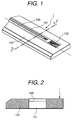
- Fig. 1 is a diagrammatic, perspective view of a conventional photoelectric conversion apparatus
- Fig. 2 is a diagrammatic cross section thereof when the photoelectric conversion apparatus is cut along 2-2 in Fig. 1.
- reference numeral 1 designates a photosensor, 101 a sensor substrate, 102 photoelectric conversion elements, 103 a wiring part, 104 a mount plate, and 105 a transparent protection layer.
- a lot of photoelectric conversion elements 102 are arranged in line on the sensor substrate 101, and the transparent protection layer 105 comprised of a thin glass plate or the like is provided on the photoelectric conversion elements 102 in order to protect the photoelectric conversion elements 102 and to be a spacer between the photoelectric conversion elements 102 and the original.
- Output signals from the photoelectric conversion elements 102 are arranged as capable of being output to the outside through the wiring part 103.
- These sensor substrate 101, photoelectric conversion elements 102, wiring part 103, and transparent protection layer 105 are incorporated with the mount plate 104, thus composing the photoelectric conversion apparatus 1.
- the mount plate 104 is made of an easily-moldable material such as a resin, and is molded except for an optically transparent portion of the member.
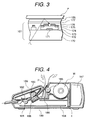
- Fig. 3 is a diagrammatic cross section for illustrating an example of the photoelectric conversion element.
- reference numeral 170 is a substrate, 171 a light-shielding layer, for example, of aluminum or chromium, 172 an insulator layer, for example, of silicon nitride, 173 a semiconductor layer, for example, of i-type amorphous silicon, 174 an ohmic contact layer, for example, of n+-type non-single-crystal silicon, 175 an electrode layer, for example, of aluminum, 176 a passivation layer, for example, of silicon nitride or polyimide, and 177 an adhesive layer, for example, of an epoxy resin.
- a light-shielding layer for example, of aluminum or chromium
- 172 an insulator layer, for example, of silicon nitride
- 173 a semiconductor layer, for example, of i-type amorphous silicon
- 174 an ohmic contact layer,
- the sensor substrate 101 has a photoelectric conversion element having the light-shielding layer 171 provided on the substrate 170 in correspondence to a photoelectric conversion portion so as to prevent illumination light from the substrate side from entering the photoelectric conversion portion, the insulator layer 172 provided on the light-shielding layer 171, the semiconductor layer 173 provided on the insulator layer, and the electrode layer 175 provided through the ohmic contact layer 174 above the semiconductor layer with a space for an incident area of light, and the passivation layer 176 provided on the photoelectric conversion element; and the transparent protection layer 105 is provided through the adhesive layer 177 above the sensor substrate 101.
- Light L emitted from an unrepresented light source passes through the sensor substrate 101, adhesive layer 177, and transparent protection layer 105 to reach the original P, and reflected light from the original P is incident to the space formed in the electrode layer 175 to be photoelectrically converted according to the incidence of light.
- Fig. 4 is a diagrammatic, sectional, structural drawing for illustrating an example of a facsimile device with a communication function as an example of the information processing apparatus having the above photoelectric conversion apparatus.
- reference numeral 180 denotes the facsimile device, 181 a feed roller, 182 a separator pawl, 183 a conveying roller, 184 a system control substrate, 185 a platen roller, 186 a recording head, 187 a power supply section, 188 the photoelectric conversion apparatus, 189 an operation panel, P the original, and W a recording medium.
- the facsimile device 180 supplies the original P to an image reading section by the feed roller 181 when the original P is inserted thereinto.
- the photoelectric conversion apparatus 188 is disposed and the original P is conveyed as urged against the reading portion by the conveying roller 183 opposed to the photoelectric conversion apparatus 188.
- This urging is effected by an urging device such as a spring, not shown.
- the separator pawl 182 is used for separating and feeding the originals P set in pile one by one.
- the facsimile device 180 has the recording head 186 for recording an image received or information read by the above photoelectric conversion apparatus 188 in a recording medium W, and the platen roller 185 for conveying the recording medium W for recording information by the recording head 186.
- the power supply 187 is a power-supply portion for driving the facsimile device 180
- the system controller 184 is provided for controlling an image reading means including the photoelectric conversion apparatus 188 and the recording means including the recording head 186
- the operation panel 189 is a so-called control portion of the facsimile device 180.
- the photoelectric conversion apparatus 188 is mounted, as shown, to a frame 4 (a main body frame in the drawing) provided in the facsimile device 180.
- This frame is normally provided in order to attain mainly the strength of the apparatus main body.
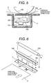
- Fig. 5 is a diagrammatic, structural drawing for illustrating a mounting portion of the photoelectric conversion apparatus 188 and surroundings thereof.
- reference numeral 191 represents a light source such as light-emitting diodes, 192 a sensor frame, 193 a light-source substrate, and 194 a connector.
- a light source such as light-emitting diodes
- 192 a sensor frame
- 193 a light-source substrate
- 194 a connector.
- the photosensor 1 and light-source substrate 193 are mounted to the sensor frame 192 so as to be incorporated therewith, thereby composing the photoelectric conversion apparatus 188.
- the connector 194 is provided for supplying the power for driving the photoelectric conversion elements or the light-emitting diodes and/or for outputting electric signals carrying information output from the photoelectric conversion elements.
- the photoelectric conversion apparatus 188 is mounted by unrepresented means in a recess formed in the frame 4.
- Fig. 6 is a diagrammatic, perspective assembly drawing for illustrating the mounting portion of the photoelectric conversion apparatus 188 and surroundings thereof.
- reference numeral 195 stands for a flexible board for outputting signals from the photosensor 1, 196 a flexible board for outputting the signals from the photoelectric conversion apparatus 188 to the outside, and 197 an electric connection portion in Fig. 7 to be connected with the flexible board.
- the photoelectric conversion apparatus 188 is arranged so as to be dropped into the recess formed in the frame 4, and the flexible board 196 is connected to the electric connection portion on the apparatus body side, thereby electrically being connected with the apparatus body.
- the conveying roller 183 is disposed above the reading portion of the photoelectric conversion apparatus 188, as described above.
- the signal line from the photosensor 1 is first electrically connected through the flexible board 195 to the light-source substrate 193 and then electrically connected through a signal processing circuit provided in the light-source substrate 193 and through the flexible board 196 to a processing circuit on the apparatus body side.
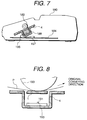
- Fig. 7 is a diagrammatic, structural drawing for illustrating an example of the connection relation between the photoelectric conversion apparatus 188 and the system control substrate 184 in the facsimile device 180.
- the flexible board 196 from the photoelectric conversion apparatus 188 is electrically connected with the connector 197 formed in the system control substrate 184.
- the present invention has been accomplished in view of the above problems, and an object of the present invention is to provide photoelectric conversion apparatus and information processing apparatus having achieved further reductions of cost, size, and weight.
- Another object of the present invention is to provide photoelectric conversion apparatus and information processing apparatus enhanced in freedom of engineering design and in freedom of design.
- a further object of the present invention is to provide an information processing apparatus comprising: a photoelectric conversion apparatus having a substrate in which a light source is arranged, and a photosensor having a plurality of photoelectric conversion elements disposed on an optically transparent substrate, an optically transparent protection layer disposed on the photoelectric conversion elements, and a mounting member, which has a projecting portion to be joined with the substrate in which the light source is arranged, on the side of the substrate in which the light source is arranged, and which unifies the optically transparent substrate with the optically transparent protection layer; a frame for the photoelectric conversion apparatus to be set thereon; conveying means for conveying the original; and a controller for controlling at least the light source, photoelectric conversion elements, and conveying means.
- Still another object of the present invention is to provide an information processing apparatus comprising a substrate in which a light source is arranged; a photosensor having a plurality of photoelectric conversion elements disposed on an optically transparent substrate and an optically transparent protection layer disposed on the photoelectric conversion elements; a frame for the substrate and the photosensor to be set thereon; conveying means for conveying the original; and a controller for controlling at least the light source, photoelectric conversion elements, and conveying means.
- a still further object of the present invention is to provide a photoelectric conversion apparatus comprising a substrate in which a light source is arranged; and a photosensor having a plurality of photoelectric conversion elements disposed on an optically transparent substrate, an optically transparent protection layer disposed on the photoelectric conversion elements, and a mounting member, which has a projecting portion to be joined with the substrate in which the light source is arranged, on the side of the substrate in which the light source is arranged, and which unifies the optically transparent substrate with the optically transparent protection layer.
- an information processing apparatus comprising: a photoelectric conversion apparatus having a substrate in which a light source is arranged, and a photosensor having a plurality of photoelectric conversion elements disposed on an optically transparent substrate, an optically transparent protection layer disposed on the photoelectric conversion elements, and a mounting member, which has a projecting portion to be joined with the substrate in which the light source is arranged, on the side of the substrate in which the light source is arranged, and which unifies the optically transparent substrate with the optically transparent protection layer; a frame for the photoelectric conversion apparatus to be set thereon; conveying means for conveying the original; and a controller for controlling at least the light source, photoelectric conversion elements, and conveying means.
- an information processing apparatus comprising a substrate in which a light source is arranged; a photosensor having a plurality of photoelectric conversion elements disposed on an optically transparent substrate and an optically transparent protection layer disposed on the photoelectric conversion elements; a frame for the substrate and the photosensor to be set thereon; conveying means for conveying the original; and a controller for controlling at least the light source, photoelectric conversion elements, and conveying means.
- a photoelectric conversion apparatus comprising a substrate in which a light source is arranged; and a photosensor having a plurality of photoelectric conversion elements disposed on an optically transparent substrate, an optically transparent protection layer disposed on the photoelectric conversion elements, and a mounting member, which has a projecting portion to be joined with the substrate in which the light source is arranged, on the side of the substrate in which the light source is arranged, and which unifies the optically transparent substrate with the optically transparent protection layer.
- the apparatus can be reduced in size and weight by those of the sensor frame. Also, the number of components is decreased, thereby further decreasing the cost and further improving the reliability, and further enabling to have the freedom of design.
- mounting to the frame of the apparatus body can be done part by part like the photosensor and the light-source substrate, and thus, in case of necessity of part exchange arising, only one desired to change can be exchanged.
- the present invention permits the light-source substrate to be unified with another electric circuit substrate, whereby the number of components can be decreased, and the reliability can be improved with decreases in numbers of assembling steps and wiring connections.
- the present invention obviates a need to use the sensor frame as a constituent member of the photosensor and to use an independent substrate for light source, whereby the length can be decreased between the reading surface side of the photosensor and the back side of the apparatus body below the electric circuit substrate such as the system control substrate, thereby achieving further reductions of size and weight.
- the present invention can improve the position accuracy between the photosensor and the light source by fitting of the electric circuit substrate having the light source with the photosensor, and assembling becomes easier. Since adjustment in light quantity of the light source and adjustment in sensitivity of the sensor can be performed in such a state that the photosensor and the light source are mounted on the electric circuit substrate like the system control substrate, the adjustments are very easy and the total number of steps can be decreased, thereby further improving the work efficiency.
- press contact between the photosensor and the conveying roller can be achieved by providing urging means such as a spring on the conveying roller side, and, utilizing an elastic force of a member forming the frame, the elastic force of the frame can be utilized as an urging force toward the conveying roller.
- urging means such as a spring on the conveying roller side
- the elastic force of the frame can be utilized as an urging force toward the conveying roller.
- the number of components can be further more decreased.
- the present invention permits curvature or deformation of the electric circuit substrate like the system control substrate in which the photosensor is mounted, to be absorbed by providing the urging means for urging the photosensor toward the conveying roller, on the photosensor side, thereby achieving further-higher-resolution reading as well as the reductions of size and weight.
- balancing becomes easier by providing the urging means on the photosensor side than by providing the urging means on the conveying roller side, and it also facilitates prevention of oblique conveyance of original as effected by giving a greater pressure in the central portion of the conveying roller as compared with the other portions.
- the urging force it is preferred to adjust the urging force so that the conveying force becomes stronger in the central portion in the longitudinal direction of the conveying roller 183 in order to prevent the oblique conveyance of original.
- the urging force is provided from the photosensor 1 side as in the embodiments presented, it can be achieved, for example, by increasing the thickness of the center spring. Thus, it becomes possible to solve the problem of oblique conveyance etc. by simple adjustment.
- Fig. 8 is a diagrammatic, structural drawing for illustrating a preferred example of the reading portion of the information processing apparatus of the present invention and surroundings thereof, Fig. 9 a diagrammatic, perspective, assembly drawing thereof, and Fig. 10 a drawing to show an example of layout in the apparatus body.
- the present embodiment shows a facsimile device 180 as an example of the information processing apparatus.
- the light-source substrate 193 in which light sources 191 are arranged at desired intervals is dropped into a recess portion formed in the frame 4.
- the light-source substrate 193 in which the light sources 191 are arranged is positioned and fixed on the bottom of the recess portion formed in the frame 4.
- the light sources 191 are electrically connected with a drive power supply through wiring such as an unrepresented connector or an unrepresented flexible board.
- the frame in the present invention is a member which can be used to provide the strength of the main body of the information processing apparatus, and which can be used as a reference of positions or dimensions of various parts or which can be used for mounting the main constituent components thereto.
- Simpler arrangement can be achieved by constructing the light-source substrate 193 in minimum patterns for drive of the light sources 191, and noise can be suppressed by placing a processing circuit for signals from the photosensor 1 on the side of the system control substrate, which can obviate a need to employ double-sided packaging for forming wiring and processing circuitry in the light-source substrate 193.
- the light-source substrate 193 may be fixed to the frame 4 by a desired method, for example adhesion, mechanical fixing, etc.
- the fixing method by adhesion may include not only coating of an adhesive, but also adhesion by a double-sided adhesive tape.
- the mechanical fixing may include snap fit, screwing, and a method of urging or pressing the substrate by hooklike fixing members or the like formed in parts of the frame 4.
- This fixing method may be any other method as long as desired fixing is effected, and thus, there is no specific restriction on the fixing method.
- the photosensor 1 is mounted in the upper part of frame 4. In this case, it is preferred to position the mount position of the photosensor 1 by providing projecting portions, which become fitting portions for fitting between the mounting portion of the photosensor 1 and the frame 4, and portions (for example, cut portions) corresponding to the projecting portions, and letting them fit each other, as shown.
- the positioning with fitting for the photosensor 1 is a preferred embodiment but is not indispensable.
- the photosensor 1 may be fixed by adhesion fixing or mechanical fixing, or by the both.
- the fixing by adhesion is achieved by application of an adhesive, a so-called double-sided tape or the like in which an adhesive is applied on the both surfaces of a base material, or a combination thereof. Any adhesive can be used herein as long as it gives no damage on the photosensor 1 or the frame 4.
- the mechanical fixing can be achieved by screwing, snap fit, press fixing, or any combination thereof.
- the press fixing can be achieved, for example, by sandwiching the photosensor 1 between a plate member and the frame 4. In this case, the plate member for pressing may be fixed to the frame 4 or another apparatus body by adhesion or mechanical fixing. It is also needless to mention that for mechanical fixing an angle bar for example having an L-shaped cross section or another mounting means can be used irrespective of whether screwing, snap fit, or pressing.
- the flexible board 195 extending from the photosensor 1 is electrically connected to an electrical connection portion 197 provided in the system control substrate 184.
- the frame 4 is one of constituent members of the apparatus body.
- the frame 4 is formed by processing a metal plate by press working, combining metal plates, using a resin such as plastics, or any combination thereof. If the frame 4 is one formed by molding of a resin, it can be molded readily in a desired shape and can be formed in a complicated shape, thus being capable of achieving a further decrease in the number of components.
- the recess formed in the frame 4 has the bottom formed in parallel with the position where the photosensor 1 is to be located, in order to set the light-source substrate 193 in parallel with the photosensor 1, but the surface of the bottom does not always have to be parallel with the position where the photosensor 1 is to be located.
- the point is that light emitted from the light sources 191 impinges upon the original and reflected light therefrom is incident to the photoelectric conversion elements. Nevertheless, a desired arrangement is that the light emitted from the light sources 191 efficiently illuminates the original and the reflected light from the original efficiently enters the photoelectric conversion elements. It becomes, however, possible to give more freedom of design by inclining the bottom of the recess in the frame 4 so as to permit inclined arrangement of the light-source substrate 193.
- the apparatus can be decreased in size and weight by those of the sensor frame. Further, since the apparatus is composed of a decreased number of components, the cost including the production cost can be decreased and the reliability can be further improved.
- the photosensor 1 and the light-source substrate 193 can be mounted separately to the frame 4 of the apparatus body, in case of necessity of part exchange arising, only the part desired to change can be exchanged.
- Fig. 11 is a diagrammatic, structural drawing for illustrating another preferred example of the reading portion of the information processing apparatus of the present invention and surroundings thereof, and Fig. 12 a diagrammatic, perspective, assembly drawing thereof.
- Fig. 11 and Fig. 12 show the example in which the light sources 191 are arranged directly on the system control substrate 184 which the apparatus body has, without using the independent light-source substrate, different from Embodiment 1.
- the system control substrate 184 is arranged to abut upon a part of the frame 4. This determines a distance between the light sources and the photosensor 1.
- an aperture is formed in the frame 4
- a framework 501 is formed as a projecting portion around the aperture
- the system control substrate 184 is made to abut on the framework 501.
- the light sources 191 are provided in the system control substrate 184, so that the system control substrate 184 can also serve as a light-source substrate.
- the photosensor 1 is arranged to fit the frame 4 in the same manner as in Embodiment 1.
- the fitting between the photosensor 1 and the frame 4 is achieved by providing the photosensor 1 with projecting portions and forming cut portions in the frame 4 in correspondence to the projecting portions, as shown.
- the relation between the projections and cuts can be reversed; that is, the projections may be formed in the frame 4 and the cuts in the photosensor 1.
- a step which the periphery of the photosensor 1 can fit may be formed around the aperture formed in the frame 4 so as to fit the entire photosensor 1.
- the fixing of the photosensor 1 to the frame may be achieved by adhesion or mechanical method in the same manner as in Embodiment 1.
- Coupling between the frame 4 and the system control substrate 184 may be achieved by adhesion or mechanical coupling, specifically by an adhesive, screws, snap fit or pressing, etc. These fixing methods each can be used alone, and of course, any combination with another method is very effective.
- a further reinforcing member such as an L-shaped angle bar can be utilized for coupling between the frame 4 and the system control substrate 184.
- a preferred arrangement is such that projections are further formed in the lower part of the framework 501 of the frame 4, apertures are formed in the system control substrate 184 in correspondence to the projections, and those projections and apertures are made to fit each other.
- the lower edges of the framework 501 have equal lengths so that the system control substrate 184 can abut upon the photosensor 1 in parallel, but, as described in Embodiment 1, the lengths may be determined so as not to be equal, in order to incline the system control substrate 184 if necessary.
- the framework 501 does not necessarily have to be formed around the entire periphery of the aperture formed in the frame 4.
- a preferred example is that the framework 501 has two edges opposed to each other.
- to form the framework 501 around the entire periphery of the aperture is preferred also in respect of improving the stiffness of frame 4.
- the material for forming the frame 4 can be one of those as explained in Embodiment 1.
- the system control substrate 184 is a substrate which includes ICs for controlling an information processing system in the case of the present embodiment, for example IC for image processing and IC for drive control of the photoelectric conversion portion, or IC for drive control of the recording unit, etc. It is a matter of course that the present invention is by no means limited to such a substrate. Namely, in the present invention, the substrate for the light sources to be arranged therein is united with the substrate having circuits arranged to achieve the other functions.
- the unification of the system control substrate 184 with the light-source substrate can decrease not only the number of substrates as a whole in the apparatus body, but also the number of connectors for wiring connections or the number of electric connection points of soldering or the like, which can decrease the number of fabrication steps of the entire information processing apparatus.
- the decreases of connectors and electric connection points can enhance the reliability, which is thus preferred.
- the present embodiment can realize the reduction in the number of components by unifying the light-source substrate with the substrate for the other electric circuits and can improve the reliability with the decreases in the number of assembling steps and in the number of wiring connections.
- the present embodiment does not need the sensor frame as a constituent member of the photosensor 1, and can shorten the distance from the reading surface side of the photosensor 1 to the back side of the apparatus body below the system control substrate 184 because it has no independent substrate for light sources, thus achieving further decreases of size and weight.
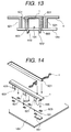
- Fig. 13 is a diagrammatic, structural drawing for illustrating another preferred example of the reading portion of the information processing apparatus of the present invention and surroundings thereof, and Fig. 14 a diagrammatic, perspective, assembly drawing thereof.
- Fig. 13 and Fig. 14 show the example in which the light-source substrate is unified with the substrate for the other electric circuits in the same manner as in Embodiment 2.
- the present embodiment is, however, arranged to mount the photosensor 1 on the system control substrate 184 of the electric circuit substrate as well as the light sources 191.
- the present embodiment is so constructed that the photosensor 1 is provided with projecting portions 601, projections 602 are provided at the lower ends of the respective projecting portions 601, and the projections 602 are hooked on the edges of holes 603 as being apertures formed in the system control substrate 184 to bring the photosensor 1 in fit with the system control substrate 184, thus unifying them with each other (which is a structure to unify members with each other by so-called snap fit).
- the photosensor 1 is preferably formed by simultaneously molding the projecting portions 601 and projections 602 upon integral plastic molding of the sensor substrate and transparent protection layer.
- the simultaneous molding of the projecting portions 601 and projections 602 can further improve positioning accuracy with respect to the array of photoelectric conversion elements formed in the sensor substrate, which results in improving the mounting accuracy to the apparatus body.
- the mounting of the photosensor 1 to the system control substrate 184 can be made firmer by further utilizing an adhesive, also using screwing, or further employing caulking.
- Abutting between the frame 4 and the system control substrate 184 can be made as explained in Embodiment 2, and the lower ends of the framework 501 can be mounted to the system control substrate 184 by snap fit in the same manner as the mounting method between the photosensor 1 and the system control substrate 184 in the present embodiment.
- system control substrate 184 may be mounted in an inclined state by changing the lengths of the framework 501 as explained in Embodiment 2 and changing the lengths of the projecting portions 601.
- the present embodiment can further improve the position accuracy of the photosensor 1 and the light sources 191 and can facilitate assembling. Since adjustment in light quantity of the light sources and adjustment in sensitivity of sensor can be performed in such a state that the photosensor and the light sources are mounted on the system control substrate 184, those adjustments become very easy and the total number of steps can be decreased, thereby further improving the work efficiency.
- Embodiment 1 to Embodiment 3 as described above employed the urging means such as a spring provided on the conveying roller 183 side for achieving press contact between the photosensor 1 and the conveying roller 183, an elastic force of the frame 4 may be utilized as an urging force toward the conveying roller 183, utilizing the elastic force of the member forming the frame 4.
- the urging means such as a spring provided on the conveying roller 183 side for achieving press contact between the photosensor 1 and the conveying roller 183
- an elastic force of the frame 4 may be utilized as an urging force toward the conveying roller 183, utilizing the elastic force of the member forming the frame 4.
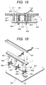
- Fig. 15 is a diagrammatic, structural drawing for illustrating another preferred example of the reading portion of the information processing apparatus of the present invention and surroundings thereof
- Fig. 16 is a diagrammatic, perspective, assembly drawing thereof.
- the light-source substrate is unified with the system control substrate 184 as being another electric circuit substrate, and projections 602 formed at the lower ends of projecting portions 601 provided for the photosensor 1 are hooked on at least parts of the peripheries of holes 603 as being apertures provided in the system control substrate 184, thus incorporating the photosensor 1 with the system control substrate 184.
- the photosensor 1 is provided with urging means 801 for urging the photosensor 1 toward the conveying roller 183.
- the projecting portions 601 are slidably engaged with the system control substrate 184, and the length from portions of the projecting portions 601 where the system control substrate 184 is in contact with the side surfaces of the photosensor 1 to portions of the projections 602 where they are in contact with the system control substrate 184 is taken longer than the thickness of the system control substrate.
- the urging means 801 also have an effect to remove mounting play of the photosensor 1 to the system control substrate 184.
- the present embodiment can absorb curvature or deformation of the system control substrate 184 by the urging means 801 such as springs in addition to the effects as explained in above Embodiment 3, thereby achieving further higher-resolution reading as well as the reductions of size and weight.
- the present embodiment has an effect to obviate balancing by providing the urging means on the photosensor 1 side as compared with the case where the urging means is provided on the conveying roller 183 side. Namely, when the conveying roller 183 is urged, the pressing force often needs to be adjusted between sides with and without power transmitting means such as gears for driving the conveying roller 183; when the urging means is provided on the photosensor 1 side as in the present embodiment, such balancing of the urging force is unnecessary.
- the present embodiment can solve the problem of oblique conveyance etc. by simple adjustment: the urging force is preferably adjusted so as to supply the strongest conveying force in the central portion of the conveying roller 183 in the longitudinal direction thereof in order to prevent the oblique conveyance of the original, which can be achieved for example by increasing the thickness of the center springs in the cases where the urging force is supplied from the photosensor 1 side as in the present embodiment.
- the present embodiment improves the tolerance zone for flatness of the photosensor 1 on the side of the conveying roller 183.
- urging means 801 does not have to be limited to this shape, but may be any urging means known as many springs or elastic members, for example elastic members such as plate springs, torsion springs, rubber, etc., balllike members having a gas such as air inside, etc.
- the photosensor applicable in the present invention is not limited to the example as described above, but can be modified with necessity. Further, the photoelectric conversion elements applicable in the present invention are not limited to the structure of the photoelectric conversion elements as described above, either. However, a preferred arrangement of the photosensor is an elongate photosensor in which the photoelectric conversion elements are arranged throughout the entire length of the reading area.
- Output methods that can be applied to the information processing apparatus etc. of the present invention include the thermal imprint recording method and the thermosensitive recording method using a thermal head, the ink jet recording method using an ink jet recording head, and the electrophotography.
- an output part of the information processing apparatus is an output means of an ink jet recording head well decreased in size and weight, excellent in plain-paper recording, and low in running cost.
- the output part is mainly explained herein.
- the recording head of a type utilizing thermal energy is more advantageous to the present invention. This is because the head itself can be made in a compact size and thus, the entire information processing apparatus can enjoy the effect of size reduction of the photoelectric conversion apparatus.
- Typical construction and principle are preferably based, for example, on the basic principle as disclosed in the specifications of United States Patents No. 4,723,129 and No. 4,740,796.
- This method can be applied to either one of the so-called on-demand type and continuous type; particularly, the method of the on-demand type is preferred because the size of the entire apparatus can be decreased.
- At least one drive signal corresponding to recording information and giving a rapid temperature rise over nucleate boiling is applied to an electrothermal converter disposed corresponding to a sheet or a conduit holding a liquid (ink), whereby thermal energy is generated in the electrothermal converter to cause film boiling on a thermal action surface of the recording head, resulting in forming a bubble in the liquid in one-to-one correspondence to the recording signal.
- the liquid is ejected through an ejection port to form at least one drop.
- the growth and contraction of bubble can be carried out immediately and appropriately, and ejection of liquid can be achieved particularly with excellent responsivity, which is more preferred.
- Preferred examples of the pulsed drive signal are those as described in the specifications of United States Patents No. 4,463,359 and No. 4,345,262. Further, more excellent recording can be performed by employing the conditions as described in the specification of United States Patent No. 4,313,124, which describes the invention as to the temperature rise rate of the above thermal action surface.
- Specific examples applicable to the structure of the recording head include the structures of a combination of ejection ports, conduits, and electrothermal converters (including linear conduits or conduits having bent portions) as described in the above specifications, and the structures using the specifications of United States Patents No. 4,558,333 and No. 4,459,600 disclosing the structures in which the thermal action surface is disposed in a curved region.
- the recording head may be one of a full-line type having the length corresponding to the width of a maximum recording medium which the recording apparatus can record.
- the recording head may be constructed to fill the length by a combination of plural recording heads or by only one recording head integrally formed, as described in the above specifications.
- the recording head include an interchangeable chip-type recording head which can complete electric connection with the apparatus body and supply of ink from the apparatus body when mounted on the apparatus body, and a recording head of a cartridge type in which electric connections and an ink tank are incorporated.
- Addition of recovery unit, preparatory assisting unit, etc. to the recording head provided as a constituent of the information processing apparatus of the present invention is preferred in order to realize further progress of maintenance free arrangement.
- effective means to stable recording are capping means, cleaning means, and pressurizing or sucking means for the recording head, heating means such as an electrothermal converter for heating the recording head, and possession of a preparatory ejection mode for effecting ejection other than recording.
- examples of recording mode may include a recording mode only by a main color such as black, and a recording mode with different multiple colors or full colors by an integrally formed recording head or a combination of plural recording heads.
- the ink may be a solid ink that is solid at room temperature or an ink that becomes softened at room temperature. Since the above ink jet method normally includes such temperature control that the viscosity of ink is kept in a stable ejection range by temperature adjustment of the ink itself in the range of 30°C to 70°C, the ink may be one that is liquid when a recording signal used is supplied. In addition, the ink may be one that is used in a liquid state after changed from a solid state by a positive temperature rise with thermal energy.
- Fig. 17 is a schematic, structural drawing for illustrating an example of the ink jet recording head, showing an ink jet recording head comprised of electrothermal converters 1103, electrodes 1104, conduits 1105, and a top plate 1106 film-formed on a substrate 1102 through steps of semiconductor fabrication process including etching, vapor deposition, sputtering, etc.
- a liquid 1112 for recording is supplied from a liquid reservoir not shown through a liquid supply pipe 1107 to a common liquid chamber 1108 in the recording head 1101.
- reference numeral 1109 designates a connector for liquid supply pipe.
- the liquid 1112 supplied into the common liquid chamber 1108 is then supplied into the conduits 1110 by the so-called capillarity, and forms a meniscus on a surface of an ejection port (orifice) at the fore end of each conduit, thereby being held stably.
- a current is supplied to an electrothermal converter 1103
- the liquid in the electrothermal converter is quickly heated to produce a bubble in the conduit, and expansion and contraction of the bubble ejects the liquid through the ejection port 1111 to form a liquid drop.
- the ink jet head can be formed in a high-density port array with a density of ejection ports being 16 nozzles/mm or more, as including 128 ejection ports or 256 ejection ports, or the ink jet head may be formed in the so-called full-line type in which the ejection ports are aligned throughout the entire recording width.
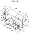
- Fig. 18 is a perspective view to show the scheme of external structure of the output portion using the ink jet recording method.
- numeral 1801 denotes the ink jet recording head (hereinafter referred to as a recording head) for recording a desired image by ejecting the ink, based on a predetermined recording signal, and 1802 a carriage for scan-moving the recording head 1801 in a recording direction (main scan direction).
- the carriage 1802 is slidably supported by guide shafts 1803, 1804 and translationally moves in the main scan direction in synchronization with a timing belt 1808.
- the timing belt 1808 engaged with pulleys 1806, 1807 is driven by a carriage motor 1805 through the pulley 1807.
- a recording sheet 1809 is guided by a paper pan 1810 and is conveyed by an unrepresented sheet feeding roller by a pinch roller in press contact therewith.
- a sheet feeding motor 1816 is used as a drive source for this conveyance.
- the recording sheet 1809 conveyed is given a tension by a sheet discharging roller 1813 and a spur 1814 and is conveyed as being kept in close contact with a heater 1811 by a sheet stopper 1812 made of an elastic member.
- the recording sheet 1809 on which the ink ejected by the recording head 1801 is deposited is heated by the heater 1811, whereby the ink deposited is fixed on the recording sheet 1809 as evaporating water.
- Numeral 1815 denotes a unit called as a recovery system, which is for maintaining ejection characteristics in a normal state by removing a foreign substance or viscosity-increased ink deposited on the discharge ports (not shown) of the recording head 1801.
- Numeral 1818a is a cap forming a part of the recovery system 1815, which is for preventing occurrence of plugging by capping the ejection ports of the recording head 1801. It is preferred to set an ink absorber 1818 inside the cap 1818a.
- a blade 1817 Disposed on the recording area side of the recovery system 1815 is a blade 1817 arranged to come in contact with the surface on which the ejection ports of the recording head 1801 are formed, so as to clean the foreign substance or ink deposited on the surface of ejection ports.
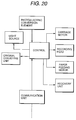
- recording is carried out, as shown in the block diagram of Fig. 20, by converting an electric signal carrying image information read by the photoelectric conversion apparatus into an electric signal for recording by image processing means and controlling the carriage motor, sheet feeding motor, recovery unit, etc. by a controller such as a CPU (central processing unit).
- a controller such as a CPU (central processing unit).
- the electric signal carrying the image information may be transmitted through a communication unit to another image processing apparatus and be output there, or information may be received through the communication unit from another information processing apparatus and be recorded by the above recording head.
- Fig. 19 shows the scheme of the output portion where the recording head 1932 of the full-line type is mounted.
- numeral 1965 is a conveying belt for conveying a recording medium, and this conveying belt 1965 conveys a recording medium not shown with rotation of a conveying roller 1964.
- the bottom surface of the recording head 1932 is an ejection port surface 1931 in which a plurality of ejection ports are arranged in correspondence to the recording area of the recording medium.
- recording can also be performed in the same manner as in the case of the serial type as described above.
- the apparatus when the method for ejecting the liquid utilizing the thermal energy as described above is used, the apparatus can be constructed in a smaller size and can perform high-resolution recording, thereby much more enhancing the effects of the present invention and making the total information processing apparatus extremely excellent.
- the present invention can realize further reductions of the size and weight, can decrease the number of constituent components in the total apparatus, can decrease the cost including the production cost, and can further improve the reliability. Further, the present invention can further improve the freedom of design.
- the components can be mounted on the frame of the apparatus body in a moderately concentrated form like the photosensor and the light-source substrate, a component or components necessitating exchange can be changed in a small and easily exchangeable unit without changing components not necessitating exchange.
- the present invention involves a unified substrate in which the light-source substrate with a light source such as LEDs, an incandescent lamp such as a halogen lamp, or a discharge tube such as a xenon tube or a fluorescent tube is unified with the electric circuit substrate in which apparatus-side electric circuits such as the system controller of apparatus are incorporated, and thus, the present invention can realize a further reduction in the number of components, a further reduction in the number of assembling steps, and a further reduction in the number of wiring connections, thereby further more improving the reliability.
- a light source such as LEDs
- an incandescent lamp such as a halogen lamp
- a discharge tube such as a xenon tube or a fluorescent tube
- the unification of the light-source substrate with the electric circuit substrate can further decrease the size and weight and can achieve a more improvement in the freedom of design.
- the hooking arrangement of the photosensor with the electric circuit substrate having the light sources can further improve the positioning accuracy between them, and can facilitate adjustment in light quantity of the light sources and adjustment in sensitivity of photosensor. Further, the present invention can further decrease the number of assembling steps as a whole, and can further improve productivity including the work efficiency.
- the present invention can also further decrease the number of components by achieving contact between the photosensor and the conveying roller utilizing the elastic force of the frame and can overcome the problem of occurrence of oblique conveyance by setting the urging means for urging the photosensor toward the conveying roller.
- the present invention can provide the photoelectric conversion apparatus and information processing apparatus that can perform stable image reading.
- a photoelectric conversion apparatus is constructed in such an arrangement that a light-source substrate 193, in which a light source 191 is arranged, and a photosensor 1 are directly mounted on a frame 4 bearing the strength of the main body of an information processing apparatus 180, the above light-source substrate 193 may be unified with an electric circuit substrate 184 of the information processing apparatus 180, and the electric circuit substrate 184 has the photosensor 1 and the light source 191, whereby the size and weight of the apparatus can be further decreased, the freedom of design and engineering design can be improved, and simplification of assembling and improvement in reliability can be achieved.
Abstract
Description
- The present invention relates to photoelectric conversion apparatus and information processing apparatus, and more particularly to photoelectric conversion apparatus suitably applicable to input portions in facsimile devices, image readers, scanners, copiers, electronic blackboards, etc., which are information processing apparatus for reading image information while relatively moving the original or the like subjected to image reading in close contact on a primary line sensor, and the information processing apparatus therewith.
- Recently, in order to further decrease the size or further enhance the performance as to the information processing apparatus such as facsimile devices, image readers, etc., elongate line sensors that can be used in a 1:1 optical system have been developed as photoelectric conversion apparatus for information processing apparatus. In order to further decrease the size and the cost, developed are photoelectric conversion apparatus and information processing apparatus for directly detecting reflected light from the original by a sensor without using a 1:1 fiber lens array but through a transparent spacer of glass or the like.
- Fig. 1 is a diagrammatic, perspective view of a conventional photoelectric conversion apparatus, and Fig. 2 is a diagrammatic cross section thereof when the photoelectric conversion apparatus is cut along 2-2 in Fig. 1. In Fig. 1 and Fig. 2,
reference numeral 1 designates a photosensor, 101 a sensor substrate, 102 photoelectric conversion elements, 103 a wiring part, 104 a mount plate, and 105 a transparent protection layer. - As shown in Fig. 1 and Fig. 2, a lot of
photoelectric conversion elements 102 are arranged in line on thesensor substrate 101, and thetransparent protection layer 105 comprised of a thin glass plate or the like is provided on thephotoelectric conversion elements 102 in order to protect thephotoelectric conversion elements 102 and to be a spacer between thephotoelectric conversion elements 102 and the original. Output signals from thephotoelectric conversion elements 102 are arranged as capable of being output to the outside through thewiring part 103. Thesesensor substrate 101,photoelectric conversion elements 102,wiring part 103, andtransparent protection layer 105 are incorporated with themount plate 104, thus composing thephotoelectric conversion apparatus 1. Themount plate 104 is made of an easily-moldable material such as a resin, and is molded except for an optically transparent portion of the member. - The structure of a photoelectric conversion element used in such a photoelectric conversion apparatus is next explained briefly referring to Fig. 3.
- Fig. 3 is a diagrammatic cross section for illustrating an example of the photoelectric conversion element. In Fig. 3,
reference numeral 170 is a substrate, 171 a light-shielding layer, for example, of aluminum or chromium, 172 an insulator layer, for example, of silicon nitride, 173 a semiconductor layer, for example, of i-type amorphous silicon, 174 an ohmic contact layer, for example, of n⁺-type non-single-crystal silicon, 175 an electrode layer, for example, of aluminum, 176 a passivation layer, for example, of silicon nitride or polyimide, and 177 an adhesive layer, for example, of an epoxy resin. - As shown in Fig. 3, the
sensor substrate 101 has a photoelectric conversion element having the light-shielding layer 171 provided on thesubstrate 170 in correspondence to a photoelectric conversion portion so as to prevent illumination light from the substrate side from entering the photoelectric conversion portion, theinsulator layer 172 provided on the light-shielding layer 171, thesemiconductor layer 173 provided on the insulator layer, and theelectrode layer 175 provided through theohmic contact layer 174 above the semiconductor layer with a space for an incident area of light, and thepassivation layer 176 provided on the photoelectric conversion element; and thetransparent protection layer 105 is provided through theadhesive layer 177 above thesensor substrate 101. - Light L emitted from an unrepresented light source passes through the
sensor substrate 101,adhesive layer 177, andtransparent protection layer 105 to reach the original P, and reflected light from the original P is incident to the space formed in theelectrode layer 175 to be photoelectrically converted according to the incidence of light. - Fig. 4 is a diagrammatic, sectional, structural drawing for illustrating an example of a facsimile device with a communication function as an example of the information processing apparatus having the above photoelectric conversion apparatus.
- In Fig. 4,
reference numeral 180 denotes the facsimile device, 181 a feed roller, 182 a separator pawl, 183 a conveying roller, 184 a system control substrate, 185 a platen roller, 186 a recording head, 187 a power supply section, 188 the photoelectric conversion apparatus, 189 an operation panel, P the original, and W a recording medium. - As shown in Fig. 4, the
facsimile device 180 supplies the original P to an image reading section by thefeed roller 181 when the original P is inserted thereinto. In the original reading section thephotoelectric conversion apparatus 188 is disposed and the original P is conveyed as urged against the reading portion by the conveyingroller 183 opposed to thephotoelectric conversion apparatus 188. This urging is effected by an urging device such as a spring, not shown. As urging the conveyingroller 183 and/or thephotoelectric conversion apparatus 188 against each other, the original P conveyed to between the conveyingroller 183 and thephotoelectric conversion apparatus 188 is further conveyed in a discharge direction. Theseparator pawl 182 is used for separating and feeding the originals P set in pile one by one. - Further, the
facsimile device 180 has therecording head 186 for recording an image received or information read by the abovephotoelectric conversion apparatus 188 in a recording medium W, and theplaten roller 185 for conveying the recording medium W for recording information by therecording head 186. - The
power supply 187 is a power-supply portion for driving thefacsimile device 180, thesystem controller 184 is provided for controlling an image reading means including thephotoelectric conversion apparatus 188 and the recording means including therecording head 186, and theoperation panel 189 is a so-called control portion of thefacsimile device 180. - The
photoelectric conversion apparatus 188 is mounted, as shown, to a frame 4 (a main body frame in the drawing) provided in thefacsimile device 180. This frame is normally provided in order to attain mainly the strength of the apparatus main body. - Fig. 5 is a diagrammatic, structural drawing for illustrating a mounting portion of the
photoelectric conversion apparatus 188 and surroundings thereof. - In Fig. 5,
reference numeral 191 represents a light source such as light-emitting diodes, 192 a sensor frame, 193 a light-source substrate, and 194 a connector. For using the light-emitting diodes as alight source 191, a plurality of light-emitting diodes are arranged at intervals on the light-source substrate 193. Thephotosensor 1 and light-source substrate 193 are mounted to thesensor frame 192 so as to be incorporated therewith, thereby composing thephotoelectric conversion apparatus 188. Theconnector 194 is provided for supplying the power for driving the photoelectric conversion elements or the light-emitting diodes and/or for outputting electric signals carrying information output from the photoelectric conversion elements. - The
photoelectric conversion apparatus 188 is mounted by unrepresented means in a recess formed in theframe 4. - Fig. 6 is a diagrammatic, perspective assembly drawing for illustrating the mounting portion of the
photoelectric conversion apparatus 188 and surroundings thereof. - In Fig. 6,
reference numeral 195 stands for a flexible board for outputting signals from thephotosensor 1, 196 a flexible board for outputting the signals from thephotoelectric conversion apparatus 188 to the outside, and 197 an electric connection portion in Fig. 7 to be connected with the flexible board. - As shown in Fig. 6, the
photoelectric conversion apparatus 188 is arranged so as to be dropped into the recess formed in theframe 4, and theflexible board 196 is connected to the electric connection portion on the apparatus body side, thereby electrically being connected with the apparatus body. Theconveying roller 183 is disposed above the reading portion of thephotoelectric conversion apparatus 188, as described above. The signal line from thephotosensor 1 is first electrically connected through theflexible board 195 to the light-source substrate 193 and then electrically connected through a signal processing circuit provided in the light-source substrate 193 and through theflexible board 196 to a processing circuit on the apparatus body side. - Fig. 7 is a diagrammatic, structural drawing for illustrating an example of the connection relation between the
photoelectric conversion apparatus 188 and thesystem control substrate 184 in thefacsimile device 180. - As shown in Fig. 7, the
flexible board 196 from thephotoelectric conversion apparatus 188 is electrically connected with theconnector 197 formed in thesystem control substrate 184. - However, with attempt to achieve further reductions of cost, size, and weight for the information processing apparatus constructed in the above structure, there was virtually no room for further reductions of cost, size, and weight, because the photoelectric conversion apparatus is constructed in a unit structure using the sensor frame. Another problem was that the limits of further reductions of size and weight would impose restrictions on freedom of engineering design of the apparatus main body or freedom of design thereof.
- The present invention has been accomplished in view of the above problems, and an object of the present invention is to provide photoelectric conversion apparatus and information processing apparatus having achieved further reductions of cost, size, and weight.
- Another object of the present invention is to provide photoelectric conversion apparatus and information processing apparatus enhanced in freedom of engineering design and in freedom of design.
- A further object of the present invention is to provide an information processing apparatus comprising: a photoelectric conversion apparatus having a substrate in which a light source is arranged, and a photosensor having a plurality of photoelectric conversion elements disposed on an optically transparent substrate, an optically transparent protection layer disposed on the photoelectric conversion elements, and a mounting member, which has a projecting portion to be joined with the substrate in which the light source is arranged, on the side of the substrate in which the light source is arranged, and which unifies the optically transparent substrate with the optically transparent protection layer; a frame for the photoelectric conversion apparatus to be set thereon; conveying means for conveying the original; and a controller for controlling at least the light source, photoelectric conversion elements, and conveying means.
- Still another object of the present invention is to provide an information processing apparatus comprising a substrate in which a light source is arranged; a photosensor having a plurality of photoelectric conversion elements disposed on an optically transparent substrate and an optically transparent protection layer disposed on the photoelectric conversion elements; a frame for the substrate and the photosensor to be set thereon; conveying means for conveying the original; and a controller for controlling at least the light source, photoelectric conversion elements, and conveying means.
- A still further object of the present invention is to provide a photoelectric conversion apparatus comprising a substrate in which a light source is arranged; and a photosensor having a plurality of photoelectric conversion elements disposed on an optically transparent substrate, an optically transparent protection layer disposed on the photoelectric conversion elements, and a mounting member, which has a projecting portion to be joined with the substrate in which the light source is arranged, on the side of the substrate in which the light source is arranged, and which unifies the optically transparent substrate with the optically transparent protection layer.
-
- Fig. 1 is a diagrammatic, perspective view for illustrating an example of the photoelectric conversion apparatus;
- Fig. 2 is a diagrammatic, sectional view of the photoelectric conversion apparatus shown in Fig. 1;
- Fig. 3 is a diagrammatic, sectional view for illustrating an example of the photoelectric conversion element;
- Fig. 4 is a diagrammatic, sectional, structural drawing for illustrating an example of the information processing apparatus having the photoelectric conversion apparatus;
- Fig. 5 is a diagrammatic, structural drawing for illustrating an example of the mounting portion of the photoelectric conversion apparatus and surroundings thereof;
- Fig. 6 is a diagrammatic, perspective, assembly drawing for illustrating an example of the mounting portion of the photoelectric conversion apparatus and surroundings thereof;
- Fig. 7 is a diagrammatic, structural drawing for illustrating an example of the electrical connection relation in a facsimile device;
- Fig. 8 is a diagrammatic, structural drawing for illustrating an example of a reading portion of an information processing apparatus of the present invention and surroundings thereof;
- Fig. 9 is a diagrammatic, perspective, assembly drawing for illustrating an example of the reading portion of the information processing apparatus of the present invention and surroundings thereof;
- Fig. 10 is a diagrammatic, sectional, layout for illustrating an example of arrangement of the main body of the information processing apparatus;
- Fig. 11 is a diagrammatic, structural drawing for illustrating an example of the reading portion of the information processing apparatus of the present invention and surroundings thereof;
- Fig. 12 is a diagrammatic, perspective, assembly drawing for illustrating an example of the reading portion of the information processing apparatus of the present invention and surroundings thereof;
- Fig. 13 is a diagrammatic, structural drawing for illustrating an example of the reading portion of the information processing apparatus of the present invention and surroundings thereof;
- Fig. 14 is a diagrammatic, perspective, assembly drawing for illustrating an example of the reading portion of the information processing apparatus of the present invention and surroundings thereof;
- Fig. 15 is a diagrammatic, structural drawing for illustrating an example of the reading portion of the information processing apparatus of the present invention and surroundings thereof;
- Fig. 16 is a diagrammatic, perspective, assembly drawing for illustrating an example of the reading portion of the information processing apparatus of the present invention and surroundings thereof;
- Fig. 17 is a diagrammatic, perspective view for illustrating an example of an ink jet recording head applicable to the information processing apparatus of the present invention;
- Fig. 18 is a diagrammatic, perspective view of an example of a recording portion using the ink jet recording method, applicable to the information processing apparatus of the present invention;
- Fig. 19 is a diagrammatic, perspective view of an example of the recording portion using the ink jet recording method, applicable to the information processing apparatus of the present invention; and
- Fig. 20 is a block structural drawing for illustrating an example of the construction of the information processing apparatus of the present invention.
- The above problems have been overcome by an information processing apparatus comprising: a photoelectric conversion apparatus having a substrate in which a light source is arranged, and a photosensor having a plurality of photoelectric conversion elements disposed on an optically transparent substrate, an optically transparent protection layer disposed on the photoelectric conversion elements, and a mounting member, which has a projecting portion to be joined with the substrate in which the light source is arranged, on the side of the substrate in which the light source is arranged, and which unifies the optically transparent substrate with the optically transparent protection layer; a frame for the photoelectric conversion apparatus to be set thereon; conveying means for conveying the original; and a controller for controlling at least the light source, photoelectric conversion elements, and conveying means.
- The above problems have also been overcome by an information processing apparatus comprising a substrate in which a light source is arranged; a photosensor having a plurality of photoelectric conversion elements disposed on an optically transparent substrate and an optically transparent protection layer disposed on the photoelectric conversion elements; a frame for the substrate and the photosensor to be set thereon; conveying means for conveying the original; and a controller for controlling at least the light source, photoelectric conversion elements, and conveying means.
- Further, the above problems have also been overcome by a photoelectric conversion apparatus comprising a substrate in which a light source is arranged; and a photosensor having a plurality of photoelectric conversion elements disposed on an optically transparent substrate, an optically transparent protection layer disposed on the photoelectric conversion elements, and a mounting member, which has a projecting portion to be joined with the substrate in which the light source is arranged, on the side of the substrate in which the light source is arranged, and which unifies the optically transparent substrate with the optically transparent protection layer.
- Since the present invention excludes the sensor frame for constructing the photoelectric conversion apparatus, the apparatus can be reduced in size and weight by those of the sensor frame. Also, the number of components is decreased, thereby further decreasing the cost and further improving the reliability, and further enabling to have the freedom of design.
- Further, mounting to the frame of the apparatus body can be done part by part like the photosensor and the light-source substrate, and thus, in case of necessity of part exchange arising, only one desired to change can be exchanged.
- In addition, the present invention permits the light-source substrate to be unified with another electric circuit substrate, whereby the number of components can be decreased, and the reliability can be improved with decreases in numbers of assembling steps and wiring connections.
- Further, the present invention obviates a need to use the sensor frame as a constituent member of the photosensor and to use an independent substrate for light source, whereby the length can be decreased between the reading surface side of the photosensor and the back side of the apparatus body below the electric circuit substrate such as the system control substrate, thereby achieving further reductions of size and weight.
- The present invention can improve the position accuracy between the photosensor and the light source by fitting of the electric circuit substrate having the light source with the photosensor, and assembling becomes easier. Since adjustment in light quantity of the light source and adjustment in sensitivity of the sensor can be performed in such a state that the photosensor and the light source are mounted on the electric circuit substrate like the system control substrate, the adjustments are very easy and the total number of steps can be decreased, thereby further improving the work efficiency.
- In the present invention press contact between the photosensor and the conveying roller can be achieved by providing urging means such as a spring on the conveying roller side, and, utilizing an elastic force of a member forming the frame, the elastic force of the frame can be utilized as an urging force toward the conveying roller. In this case, the number of components can be further more decreased.
- In addition, the present invention permits curvature or deformation of the electric circuit substrate like the system control substrate in which the photosensor is mounted, to be absorbed by providing the urging means for urging the photosensor toward the conveying roller, on the photosensor side, thereby achieving further-higher-resolution reading as well as the reductions of size and weight.
- Also, balancing becomes easier by providing the urging means on the photosensor side than by providing the urging means on the conveying roller side, and it also facilitates prevention of oblique conveyance of original as effected by giving a greater pressure in the central portion of the conveying roller as compared with the other portions.
- According to the embodiments presented, it is preferred to adjust the urging force so that the conveying force becomes stronger in the central portion in the longitudinal direction of the conveying
roller 183 in order to prevent the oblique conveyance of original. When the urging force is provided from thephotosensor 1 side as in the embodiments presented, it can be achieved, for example, by increasing the thickness of the center spring. Thus, it becomes possible to solve the problem of oblique conveyance etc. by simple adjustment. - The embodiments of the present invention will be explained by reference to the drawings.
- Fig. 8 is a diagrammatic, structural drawing for illustrating a preferred example of the reading portion of the information processing apparatus of the present invention and surroundings thereof, Fig. 9 a diagrammatic, perspective, assembly drawing thereof, and Fig. 10 a drawing to show an example of layout in the apparatus body.
- As shown in Fig. 8 to Fig. 10, the present embodiment shows a
facsimile device 180 as an example of the information processing apparatus. - In the present embodiment the light-
source substrate 193 in whichlight sources 191 are arranged at desired intervals is dropped into a recess portion formed in theframe 4. In detail, the light-source substrate 193 in which thelight sources 191 are arranged is positioned and fixed on the bottom of the recess portion formed in theframe 4. Thelight sources 191 are electrically connected with a drive power supply through wiring such as an unrepresented connector or an unrepresented flexible board. - The frame in the present invention is a member which can be used to provide the strength of the main body of the information processing apparatus, and which can be used as a reference of positions or dimensions of various parts or which can be used for mounting the main constituent components thereto.
- Simpler arrangement can be achieved by constructing the light-
source substrate 193 in minimum patterns for drive of thelight sources 191, and noise can be suppressed by placing a processing circuit for signals from thephotosensor 1 on the side of the system control substrate, which can obviate a need to employ double-sided packaging for forming wiring and processing circuitry in the light-source substrate 193. - The light-
source substrate 193 may be fixed to theframe 4 by a desired method, for example adhesion, mechanical fixing, etc. The fixing method by adhesion may include not only coating of an adhesive, but also adhesion by a double-sided adhesive tape. Further, the mechanical fixing may include snap fit, screwing, and a method of urging or pressing the substrate by hooklike fixing members or the like formed in parts of theframe 4. This fixing method may be any other method as long as desired fixing is effected, and thus, there is no specific restriction on the fixing method. - The
photosensor 1 is mounted in the upper part offrame 4. In this case, it is preferred to position the mount position of thephotosensor 1 by providing projecting portions, which become fitting portions for fitting between the mounting portion of thephotosensor 1 and theframe 4, and portions (for example, cut portions) corresponding to the projecting portions, and letting them fit each other, as shown. In addition to the arrangement in which the projecting portions to become the fitting portions, and the portions corresponding to the projecting portions are formed with the projecting portions on thephotosensor 1 side and the recessed portions corresponding to the projecting portions on theframe 4 side, as shown, another possible arrangement is such that the projecting portions are formed on theframe 4 side and the portions corresponding to the projecting portions on thephotosensor 1 side, or still another possible arrangement is that the bothphotosensor 1 andframe 4 have the projecting portions and portions corresponding to the projecting portions opposed to each other. A further preferred arrangement is that a step is formed around the side surfaces of the aperture in the recess in theframe 4 and the periphery of thephotosensor 1 is arranged to fit the step. Forming the projecting portions in thephotosensor 1 is preferred, because they can reinforce thephotosensor 1. - It is, however, noted that the positioning with fitting for the
photosensor 1 is a preferred embodiment but is not indispensable. - The
photosensor 1 may be fixed by adhesion fixing or mechanical fixing, or by the both. The fixing by adhesion is achieved by application of an adhesive, a so-called double-sided tape or the like in which an adhesive is applied on the both surfaces of a base material, or a combination thereof. Any adhesive can be used herein as long as it gives no damage on thephotosensor 1 or theframe 4. The mechanical fixing can be achieved by screwing, snap fit, press fixing, or any combination thereof. The press fixing can be achieved, for example, by sandwiching thephotosensor 1 between a plate member and theframe 4. In this case, the plate member for pressing may be fixed to theframe 4 or another apparatus body by adhesion or mechanical fixing. It is also needless to mention that for mechanical fixing an angle bar for example having an L-shaped cross section or another mounting means can be used irrespective of whether screwing, snap fit, or pressing. - The
flexible board 195 extending from thephotosensor 1 is electrically connected to anelectrical connection portion 197 provided in thesystem control substrate 184. - The
frame 4 is one of constituent members of the apparatus body. Theframe 4 is formed by processing a metal plate by press working, combining metal plates, using a resin such as plastics, or any combination thereof. If theframe 4 is one formed by molding of a resin, it can be molded readily in a desired shape and can be formed in a complicated shape, thus being capable of achieving a further decrease in the number of components. - In the present embodiment, the recess formed in the
frame 4 has the bottom formed in parallel with the position where thephotosensor 1 is to be located, in order to set the light-source substrate 193 in parallel with thephotosensor 1, but the surface of the bottom does not always have to be parallel with the position where thephotosensor 1 is to be located. The point is that light emitted from thelight sources 191 impinges upon the original and reflected light therefrom is incident to the photoelectric conversion elements. Nevertheless, a desired arrangement is that the light emitted from thelight sources 191 efficiently illuminates the original and the reflected light from the original efficiently enters the photoelectric conversion elements. It becomes, however, possible to give more freedom of design by inclining the bottom of the recess in theframe 4 so as to permit inclined arrangement of the light-source substrate 193. - Since the present embodiment does not use the sensor frame to form the photoelectric conversion apparatus, the apparatus can be decreased in size and weight by those of the sensor frame. Further, since the apparatus is composed of a decreased number of components, the cost including the production cost can be decreased and the reliability can be further improved.
- Additionally, because the
photosensor 1 and the light-source substrate 193 can be mounted separately to theframe 4 of the apparatus body, in case of necessity of part exchange arising, only the part desired to change can be exchanged. - Fig. 11 is a diagrammatic, structural drawing for illustrating another preferred example of the reading portion of the information processing apparatus of the present invention and surroundings thereof, and Fig. 12 a diagrammatic, perspective, assembly drawing thereof.
- Fig. 11 and Fig. 12 show the example in which the
light sources 191 are arranged directly on thesystem control substrate 184 which the apparatus body has, without using the independent light-source substrate, different fromEmbodiment 1. Thesystem control substrate 184 is arranged to abut upon a part of theframe 4. This determines a distance between the light sources and thephotosensor 1. - In more detail, in the case of the present embodiment, an aperture is formed in the
frame 4, aframework 501 is formed as a projecting portion around the aperture, and thesystem control substrate 184 is made to abut on theframework 501. Thelight sources 191 are provided in thesystem control substrate 184, so that thesystem control substrate 184 can also serve as a light-source substrate. - The
photosensor 1 is arranged to fit theframe 4 in the same manner as inEmbodiment 1. The fitting between thephotosensor 1 and theframe 4 is achieved by providing thephotosensor 1 with projecting portions and forming cut portions in theframe 4 in correspondence to the projecting portions, as shown. Of course, the relation between the projections and cuts can be reversed; that is, the projections may be formed in theframe 4 and the cuts in thephotosensor 1. - Also in the same manner as in the case of
Embodiment 1, a step which the periphery of thephotosensor 1 can fit may be formed around the aperture formed in theframe 4 so as to fit theentire photosensor 1. - The fixing of the
photosensor 1 to the frame may be achieved by adhesion or mechanical method in the same manner as inEmbodiment 1. - Coupling between the
frame 4 and thesystem control substrate 184 may be achieved by adhesion or mechanical coupling, specifically by an adhesive, screws, snap fit or pressing, etc. These fixing methods each can be used alone, and of course, any combination with another method is very effective. - It is needless to mention that a further reinforcing member such as an L-shaped angle bar can be utilized for coupling between the
frame 4 and thesystem control substrate 184. - In order to further enhance the mounting accuracy or in order to further improve the mounting strength, a preferred arrangement is such that projections are further formed in the lower part of the
framework 501 of theframe 4, apertures are formed in thesystem control substrate 184 in correspondence to the projections, and those projections and apertures are made to fit each other. - In the present embodiment the lower edges of the
framework 501 have equal lengths so that thesystem control substrate 184 can abut upon thephotosensor 1 in parallel, but, as described inEmbodiment 1, the lengths may be determined so as not to be equal, in order to incline thesystem control substrate 184 if necessary. - Further, the
framework 501 does not necessarily have to be formed around the entire periphery of the aperture formed in theframe 4. A preferred example is that theframework 501 has two edges opposed to each other. However, to form theframework 501 around the entire periphery of the aperture is preferred also in respect of improving the stiffness offrame 4. - The material for forming the
frame 4 can be one of those as explained inEmbodiment 1. - The
system control substrate 184 is a substrate which includes ICs for controlling an information processing system in the case of the present embodiment, for example IC for image processing and IC for drive control of the photoelectric conversion portion, or IC for drive control of the recording unit, etc. It is a matter of course that the present invention is by no means limited to such a substrate. Namely, in the present invention, the substrate for the light sources to be arranged therein is united with the substrate having circuits arranged to achieve the other functions. - The unification of the
system control substrate 184 with the light-source substrate can decrease not only the number of substrates as a whole in the apparatus body, but also the number of connectors for wiring connections or the number of electric connection points of soldering or the like, which can decrease the number of fabrication steps of the entire information processing apparatus. In addition, the decreases of connectors and electric connection points can enhance the reliability, which is thus preferred. - As explained above, the present embodiment can realize the reduction in the number of components by unifying the light-source substrate with the substrate for the other electric circuits and can improve the reliability with the decreases in the number of assembling steps and in the number of wiring connections.
- The present embodiment does not need the sensor frame as a constituent member of the
photosensor 1, and can shorten the distance from the reading surface side of thephotosensor 1 to the back side of the apparatus body below thesystem control substrate 184 because it has no independent substrate for light sources, thus achieving further decreases of size and weight. - Fig. 13 is a diagrammatic, structural drawing for illustrating another preferred example of the reading portion of the information processing apparatus of the present invention and surroundings thereof, and Fig. 14 a diagrammatic, perspective, assembly drawing thereof.
- Fig. 13 and Fig. 14 show the example in which the light-source substrate is unified with the substrate for the other electric circuits in the same manner as in
Embodiment 2. The present embodiment is, however, arranged to mount thephotosensor 1 on thesystem control substrate 184 of the electric circuit substrate as well as thelight sources 191. - Namely, the present embodiment is so constructed that the
photosensor 1 is provided with projectingportions 601,projections 602 are provided at the lower ends of the respective projectingportions 601, and theprojections 602 are hooked on the edges ofholes 603 as being apertures formed in thesystem control substrate 184 to bring thephotosensor 1 in fit with thesystem control substrate 184, thus unifying them with each other (which is a structure to unify members with each other by so-called snap fit). - The
photosensor 1 is preferably formed by simultaneously molding the projectingportions 601 andprojections 602 upon integral plastic molding of the sensor substrate and transparent protection layer. The simultaneous molding of the projectingportions 601 andprojections 602 can further improve positioning accuracy with respect to the array of photoelectric conversion elements formed in the sensor substrate, which results in improving the mounting accuracy to the apparatus body. - Of course, the mounting of the
photosensor 1 to thesystem control substrate 184 can be made firmer by further utilizing an adhesive, also using screwing, or further employing caulking. - Abutting between the
frame 4 and thesystem control substrate 184 can be made as explained inEmbodiment 2, and the lower ends of theframework 501 can be mounted to thesystem control substrate 184 by snap fit in the same manner as the mounting method between thephotosensor 1 and thesystem control substrate 184 in the present embodiment. - Also in the present embodiment, the
system control substrate 184 may be mounted in an inclined state by changing the lengths of theframework 501 as explained inEmbodiment 2 and changing the lengths of the projectingportions 601. - The present embodiment can further improve the position accuracy of the
photosensor 1 and thelight sources 191 and can facilitate assembling. Since adjustment in light quantity of the light sources and adjustment in sensitivity of sensor can be performed in such a state that the photosensor and the light sources are mounted on thesystem control substrate 184, those adjustments become very easy and the total number of steps can be decreased, thereby further improving the work efficiency. - Although
Embodiment 1 to Embodiment 3 as described above employed the urging means such as a spring provided on the conveyingroller 183 side for achieving press contact between thephotosensor 1 and the conveyingroller 183, an elastic force of theframe 4 may be utilized as an urging force toward the conveyingroller 183, utilizing the elastic force of the member forming theframe 4. - Fig. 15 is a diagrammatic, structural drawing for illustrating another preferred example of the reading portion of the information processing apparatus of the present invention and surroundings thereof, and Fig. 16 is a diagrammatic, perspective, assembly drawing thereof.
- In Fig. 15 and Fig. 16, similarly as in Embodiment 3, the light-source substrate is unified with the
system control substrate 184 as being another electric circuit substrate, andprojections 602 formed at the lower ends of projectingportions 601 provided for thephotosensor 1 are hooked on at least parts of the peripheries ofholes 603 as being apertures provided in thesystem control substrate 184, thus incorporating thephotosensor 1 with thesystem control substrate 184. - In the present embodiment the
photosensor 1 is provided with urging means 801 for urging thephotosensor 1 toward the conveyingroller 183. In order to enable thephotosensor 1 urged toward the conveying roller by the urging means 801 to move to the light source side in the drawing when thephotosensor 1 receives a force against the urging means 801, that is, in order to enable the photosensor urged by the urging means to move along the projecting portions as the photosensor pushes the conveying roller and the original is conveyed, the projectingportions 601 are slidably engaged with thesystem control substrate 184, and the length from portions of the projectingportions 601 where thesystem control substrate 184 is in contact with the side surfaces of thephotosensor 1 to portions of theprojections 602 where they are in contact with thesystem control substrate 184 is taken longer than the thickness of the system control substrate. The urging means 801 also have an effect to remove mounting play of thephotosensor 1 to thesystem control substrate 184. - The present embodiment can absorb curvature or deformation of the
system control substrate 184 by the urging means 801 such as springs in addition to the effects as explained in above Embodiment 3, thereby achieving further higher-resolution reading as well as the reductions of size and weight. - In particular, the present embodiment has an effect to obviate balancing by providing the urging means on the
photosensor 1 side as compared with the case where the urging means is provided on the conveyingroller 183 side. Namely, when the conveyingroller 183 is urged, the pressing force often needs to be adjusted between sides with and without power transmitting means such as gears for driving the conveyingroller 183; when the urging means is provided on thephotosensor 1 side as in the present embodiment, such balancing of the urging force is unnecessary. - The present embodiment can solve the problem of oblique conveyance etc. by simple adjustment: the urging force is preferably adjusted so as to supply the strongest conveying force in the central portion of the conveying
roller 183 in the longitudinal direction thereof in order to prevent the oblique conveyance of the original, which can be achieved for example by increasing the thickness of the center springs in the cases where the urging force is supplied from thephotosensor 1 side as in the present embodiment. - Further, the present embodiment improves the tolerance zone for flatness of the
photosensor 1 on the side of the conveyingroller 183. - Although Fig. 16 showed the example in which the above urging means is coil springs, the urging means 801 does not have to be limited to this shape, but may be any urging means known as many springs or elastic members, for example elastic members such as plate springs, torsion springs, rubber, etc., balllike members having a gas such as air inside, etc.
- The photosensor applicable in the present invention is not limited to the example as described above, but can be modified with necessity. Further, the photoelectric conversion elements applicable in the present invention are not limited to the structure of the photoelectric conversion elements as described above, either. However, a preferred arrangement of the photosensor is an elongate photosensor in which the photoelectric conversion elements are arranged throughout the entire length of the reading area.
- The reading portion used in the information processing apparatus of the present invention is next explained by reference to the drawings.
- Output methods that can be applied to the information processing apparatus etc. of the present invention include the thermal imprint recording method and the thermosensitive recording method using a thermal head, the ink jet recording method using an ink jet recording head, and the electrophotography.
- Among these many methods, here is explained a structural example where an output part of the information processing apparatus is an output means of an ink jet recording head well decreased in size and weight, excellent in plain-paper recording, and low in running cost. The output part is mainly explained herein.
- In the ink jet recording method, use of the recording head of a type utilizing thermal energy is more advantageous to the present invention. This is because the head itself can be made in a compact size and thus, the entire information processing apparatus can enjoy the effect of size reduction of the photoelectric conversion apparatus.
- Typical construction and principle are preferably based, for example, on the basic principle as disclosed in the specifications of United States Patents No. 4,723,129 and No. 4,740,796. This method can be applied to either one of the so-called on-demand type and continuous type; particularly, the method of the on-demand type is preferred because the size of the entire apparatus can be decreased.
- Briefly explaining this method, at least one drive signal corresponding to recording information and giving a rapid temperature rise over nucleate boiling is applied to an electrothermal converter disposed corresponding to a sheet or a conduit holding a liquid (ink), whereby thermal energy is generated in the electrothermal converter to cause film boiling on a thermal action surface of the recording head, resulting in forming a bubble in the liquid in one-to-one correspondence to the recording signal. Based on growth and contraction of the bubble, the liquid is ejected through an ejection port to form at least one drop. Employing a pulsed form for the drive signal, the growth and contraction of bubble can be carried out immediately and appropriately, and ejection of liquid can be achieved particularly with excellent responsivity, which is more preferred.
- Preferred examples of the pulsed drive signal are those as described in the specifications of United States Patents No. 4,463,359 and No. 4,345,262. Further, more excellent recording can be performed by employing the conditions as described in the specification of United States Patent No. 4,313,124, which describes the invention as to the temperature rise rate of the above thermal action surface.
- Specific examples applicable to the structure of the recording head include the structures of a combination of ejection ports, conduits, and electrothermal converters (including linear conduits or conduits having bent portions) as described in the above specifications, and the structures using the specifications of United States Patents No. 4,558,333 and No. 4,459,600 disclosing the structures in which the thermal action surface is disposed in a curved region.
- In addition, other effective structures are those based on the bulletin of Japanese Laid-open Patent Application No. 59-123670 disclosing the structure having a common slit as an ejecting portion of liquid and the bulletin of Japanese Laid-open Patent Application No. 59-138461 disclosing the structure to correspond apertures for absorbing pressure waves of thermal energy to the ejecting portion.
- Further, the recording head may be one of a full-line type having the length corresponding to the width of a maximum recording medium which the recording apparatus can record. In this case, the recording head may be constructed to fill the length by a combination of plural recording heads or by only one recording head integrally formed, as described in the above specifications.
- Additionally, preferred examples of the recording head include an interchangeable chip-type recording head which can complete electric connection with the apparatus body and supply of ink from the apparatus body when mounted on the apparatus body, and a recording head of a cartridge type in which electric connections and an ink tank are incorporated.
- Addition of recovery unit, preparatory assisting unit, etc. to the recording head provided as a constituent of the information processing apparatus of the present invention is preferred in order to realize further progress of maintenance free arrangement.
- Specifically describing those units, effective means to stable recording are capping means, cleaning means, and pressurizing or sucking means for the recording head, heating means such as an electrothermal converter for heating the recording head, and possession of a preparatory ejection mode for effecting ejection other than recording.
- Further, examples of recording mode may include a recording mode only by a main color such as black, and a recording mode with different multiple colors or full colors by an integrally formed recording head or a combination of plural recording heads.
- The above description concerned examples with liquid (ink), but the ink may be a solid ink that is solid at room temperature or an ink that becomes softened at room temperature. Since the above ink jet method normally includes such temperature control that the viscosity of ink is kept in a stable ejection range by temperature adjustment of the ink itself in the range of 30°C to 70°C, the ink may be one that is liquid when a recording signal used is supplied. In addition, the ink may be one that is used in a liquid state after changed from a solid state by a positive temperature rise with thermal energy.
- Next explained briefly is an ink jet recording head used in the method of performing recording with ejection of liquid utilizing the thermal energy as described.
- Fig. 17 is a schematic, structural drawing for illustrating an example of the ink jet recording head, showing an ink jet recording head comprised of
electrothermal converters 1103,electrodes 1104,conduits 1105, and atop plate 1106 film-formed on asubstrate 1102 through steps of semiconductor fabrication process including etching, vapor deposition, sputtering, etc. A liquid 1112 for recording is supplied from a liquid reservoir not shown through aliquid supply pipe 1107 to acommon liquid chamber 1108 in therecording head 1101. In the drawing,reference numeral 1109 designates a connector for liquid supply pipe. - The liquid 1112 supplied into the
common liquid chamber 1108 is then supplied into theconduits 1110 by the so-called capillarity, and forms a meniscus on a surface of an ejection port (orifice) at the fore end of each conduit, thereby being held stably. When a current is supplied to anelectrothermal converter 1103, the liquid in the electrothermal converter is quickly heated to produce a bubble in the conduit, and expansion and contraction of the bubble ejects the liquid through theejection port 1111 to form a liquid drop. - According to the above arrangement, the ink jet head can be formed in a high-density port array with a density of ejection ports being 16 nozzles/mm or more, as including 128 ejection ports or 256 ejection ports, or the ink jet head may be formed in the so-called full-line type in which the ejection ports are aligned throughout the entire recording width.
- Fig. 18 is a perspective view to show the scheme of external structure of the output portion using the ink jet recording method.
- In the drawing, numeral 1801 denotes the ink jet recording head (hereinafter referred to as a recording head) for recording a desired image by ejecting the ink, based on a predetermined recording signal, and 1802 a carriage for scan-moving the
recording head 1801 in a recording direction (main scan direction). Thecarriage 1802 is slidably supported byguide shafts timing belt 1808. Thetiming belt 1808 engaged withpulleys carriage motor 1805 through thepulley 1807. - A
recording sheet 1809 is guided by apaper pan 1810 and is conveyed by an unrepresented sheet feeding roller by a pinch roller in press contact therewith. - A
sheet feeding motor 1816 is used as a drive source for this conveyance. Therecording sheet 1809 conveyed is given a tension by asheet discharging roller 1813 and aspur 1814 and is conveyed as being kept in close contact with aheater 1811 by asheet stopper 1812 made of an elastic member. Therecording sheet 1809 on which the ink ejected by therecording head 1801 is deposited is heated by theheater 1811, whereby the ink deposited is fixed on therecording sheet 1809 as evaporating water. -
Numeral 1815 denotes a unit called as a recovery system, which is for maintaining ejection characteristics in a normal state by removing a foreign substance or viscosity-increased ink deposited on the discharge ports (not shown) of therecording head 1801. - Numeral 1818a is a cap forming a part of the
recovery system 1815, which is for preventing occurrence of plugging by capping the ejection ports of therecording head 1801. It is preferred to set anink absorber 1818 inside thecap 1818a. - Disposed on the recording area side of the
recovery system 1815 is ablade 1817 arranged to come in contact with the surface on which the ejection ports of therecording head 1801 are formed, so as to clean the foreign substance or ink deposited on the surface of ejection ports. - In the present invention, recording is carried out, as shown in the block diagram of Fig. 20, by converting an electric signal carrying image information read by the photoelectric conversion apparatus into an electric signal for recording by image processing means and controlling the carriage motor, sheet feeding motor, recovery unit, etc. by a controller such as a CPU (central processing unit).
- The electric signal carrying the image information may be transmitted through a communication unit to another image processing apparatus and be output there, or information may be received through the communication unit from another information processing apparatus and be recorded by the above recording head.
- Next, Fig. 19 shows the scheme of the output portion where the
recording head 1932 of the full-line type is mounted. - In Fig. 19, numeral 1965 is a conveying belt for conveying a recording medium, and this conveying
belt 1965 conveys a recording medium not shown with rotation of a conveyingroller 1964. The bottom surface of therecording head 1932 is anejection port surface 1931 in which a plurality of ejection ports are arranged in correspondence to the recording area of the recording medium. - In this case recording can also be performed in the same manner as in the case of the serial type as described above.
- Of course, the above output portion is explained as an example, and there are a lot of modifications thereof.
- However, when the method for ejecting the liquid utilizing the thermal energy as described above is used, the apparatus can be constructed in a smaller size and can perform high-resolution recording, thereby much more enhancing the effects of the present invention and making the total information processing apparatus extremely excellent.
- As explained above, the present invention can realize further reductions of the size and weight, can decrease the number of constituent components in the total apparatus, can decrease the cost including the production cost, and can further improve the reliability. Further, the present invention can further improve the freedom of design.
- Since the components can be mounted on the frame of the apparatus body in a moderately concentrated form like the photosensor and the light-source substrate, a component or components necessitating exchange can be changed in a small and easily exchangeable unit without changing components not necessitating exchange.
- In addition, the present invention involves a unified substrate in which the light-source substrate with a light source such as LEDs, an incandescent lamp such as a halogen lamp, or a discharge tube such as a xenon tube or a fluorescent tube is unified with the electric circuit substrate in which apparatus-side electric circuits such as the system controller of apparatus are incorporated, and thus, the present invention can realize a further reduction in the number of components, a further reduction in the number of assembling steps, and a further reduction in the number of wiring connections, thereby further more improving the reliability.
- Further, the unification of the light-source substrate with the electric circuit substrate can further decrease the size and weight and can achieve a more improvement in the freedom of design.
- In addition, the hooking arrangement of the photosensor with the electric circuit substrate having the light sources can further improve the positioning accuracy between them, and can facilitate adjustment in light quantity of the light sources and adjustment in sensitivity of photosensor. Further, the present invention can further decrease the number of assembling steps as a whole, and can further improve productivity including the work efficiency.
- The present invention can also further decrease the number of components by achieving contact between the photosensor and the conveying roller utilizing the elastic force of the frame and can overcome the problem of occurrence of oblique conveyance by setting the urging means for urging the photosensor toward the conveying roller.
- Additionally, the present invention can provide the photoelectric conversion apparatus and information processing apparatus that can perform stable image reading.
- It should be noted that the present invention is by no means intended to be limited to the above embodiments and drawings, but they may be properly modified or combined within the scope of the essence of the present invention.
- A photoelectric conversion apparatus is constructed in such an arrangement that a light-
source substrate 193, in which alight source 191 is arranged, and aphotosensor 1 are directly mounted on aframe 4 bearing the strength of the main body of aninformation processing apparatus 180, the above light-source substrate 193 may be unified with anelectric circuit substrate 184 of theinformation processing apparatus 180, and theelectric circuit substrate 184 has thephotosensor 1 and thelight source 191, whereby the size and weight of the apparatus can be further decreased, the freedom of design and engineering design can be improved, and simplification of assembling and improvement in reliability can be achieved.
Claims (52)
- An information processing apparatus comprising: a photoelectric conversion apparatus having a substrate in which a light source is arranged, and a photosensor having a plurality of photoelectric conversion elements disposed on an optically transparent substrate, an optically transparent protection layer disposed on said photoelectric conversion elements, and a mounting member, which has a projecting portion to be joined with said substrate in which the light source is arranged, on the side of said substrate in which the light source is arranged, and which unifies said optically transparent substrate with said optically transparent protection layer; a frame for said photoelectric conversion apparatus to be set thereon; conveying means for conveying an original; and a controller for controlling at least said light source, photoelectric conversion elements, and conveying means.
- The information processing apparatus according to Claim 1, wherein said substrate in which the light source is arranged is joined with said projecting portion by fitting.
- The information processing apparatus according to Claim 1, wherein an aperture is formed in said substrate in which the light source is arranged and said projecting portion is set in said aperture.
- The information processing apparatus according to Claim 1, wherein said projecting portion further comprises a projection to be engaged with said substrate in which the light source is arranged.
- The information processing apparatus according to Claim 4, wherein a length from a portion of said projecting portion in said photosensor in contact with said substrate to a portion of said projection in contact with said substrate is longer than a thickness of said substrate.
- The information processing apparatus according to Claim 1, which comprises urging means for urging said photosensor in a direction in which said projections come into contact with said substrate.
- The information processing apparatus according to Claim 6, wherein said urging means is a spring or an elastic member.
- The information processing apparatus according to Claim 1, wherein said substrate is an electric circuit substrate having said controller.
- The information processing apparatus according to Claim 1, wherein said frame has a projecting portion to be engaged with said substrate.
- The information processing apparatus according to Claim 1, further comprising an output portion for recording an image according to an electric signal corresponding to image information.
- The information processing apparatus according to Claim 10, wherein said output portion has a thermal head.
- The information processing apparatus according to Claim 10, wherein said output portion has an ink jet recording head.
- The information processing apparatus according to Claim 12, wherein said ink jet recording head has an electrothermal converter for generating thermal energy for forming a bubble for ejecting an ink.
- The information processing apparatus according to Claim 12, which has recovery means for recovering a failure in ejection of said ink jet recording head.
- The information processing apparatus according to Claim 12, which has cleaning means for cleaning said ink jet recording head.
- The information processing apparatus according to Claim 12, which has capping means for capping said ink jet recording head.
- The information processing apparatus according to Claim 16, wherein said capping means has an ink absorber.
- The information processing apparatus according to Claim 15, wherein said cleaning means has a cleaning blade.
- The information processing apparatus according to Claim 10, further comprising a heater for heating a member recorded.
- The information processing apparatus according to Claim 12, wherein said ink jet recording head is a full-line head.
- The information processing apparatus according to Claim 1, wherein said frame is at least a part of a frame of the main body of said information processing apparatus.
- The information processing apparatus according to Claim 1, wherein said frame is urging means for urging said photosensor toward said conveying roller.
- An information processing apparatus comprising a substrate in which a light source is arranged; a photosensor having a plurality of photoelectric conversion elements disposed on an optically transparent substrate and an optically transparent protection layer disposed on said photoelectric conversion elements; a frame for said substrate and said photosensor to be set thereon; conveying means for conveying an original; and a controller for controlling at least said light source, photoelectric conversion elements, and conveying means.
- The information processing apparatus according to Claim 23, wherein said frame has a recess for said photosensor and said substrate to be placed therein.
- The information processing apparatus according to Claim 23, wherein said frame has an aperture and said photosensor is disposed in correspondence to said aperture.
- The information processing apparatus according to Claim 25, wherein at least a part of the periphery of said aperture has a framework as a projection.
- The information processing apparatus according to Claim 26, wherein said framework is in contact with the substrate in which the light source is arranged.
- The information processing apparatus according to Claim 27, wherein said framework is engaged with said substrate.
- The information processing apparatus according to Claim 23, wherein said photosensor is in fit with said frame.
- The information processing apparatus according to Claim 23, wherein said photosensor has a mounting member for unifying said optically transparent substrate with said optically transparent protection layer.
- The information processing apparatus according to Claim 30, wherein said photosensor has a projecting portion or a cut portion.
- The information processing apparatus according to Claim 23, further comprising an output portion for recording an image according to an electric signal corresponding to image information.
- The information processing apparatus according to Claim 32, wherein said output portion has a thermal head.
- The information processing apparatus according to Claim 32, wherein said output portion has an ink jet recording head.
- The information processing apparatus according to Claim 34, wherein said ink jet recording head has an electrothermal converter for generating thermal energy for forming a bubble for ejecting an ink.
- The information processing apparatus according to Claim 34, which has recovery means for recovering a failure in ejection of said ink jet recording head.
- The information processing apparatus according to Claim 34, which has cleaning means for cleaning said ink jet recording head.
- The information processing apparatus according to Claim 34, which has capping means for capping said ink jet recording head.
- The information processing apparatus according to Claim 38, wherein said capping means has an ink absorber.
- The information processing apparatus according to Claim 37, wherein said cleaning means has a cleaning blade.
- The information processing apparatus according to Claim 34, further comprising a heater for heating a member recorded.
- The information processing apparatus according to Claim 34, wherein said ink jet recording head is a full-line head.
- The information processing apparatus according to Claim 23, wherein said frame is at least a part of a frame of the main body of said information processing apparatus.
- The information processing apparatus according to Claim 23, wherein said frame is urging means for urging said photosensor toward said conveying roller.
- A photoelectric conversion apparatus comprising a substrate in which a light source is arranged; and a photosensor having a plurality of photoelectric conversion elements disposed on an optically transparent substrate, an optically transparent protection layer disposed on said photoelectric conversion elements, and a mounting member, which has a projecting portion to be joined with said substrate in which the light source is arranged, on the side of said substrate in which the light source is arranged, and which unifies said optically transparent substrate with said optically transparent protection layer.
- The photoelectric conversion apparatus according to Claim 45, wherein said substrate in which the light source is arranged is joined with said projecting portion by fitting.
- The photoelectric conversion apparatus according to Claim 45, wherein an aperture is formed in said substrate in which the light source is arranged and said projecting portion is set in said aperture.
- The photoelectric conversion apparatus according to Claim 45, wherein said projecting portion further comprises a projection to be engaged with said substrate in which the light source is arranged.
- The photoelectric conversion apparatus according to Claim 45, wherein a length from a portion of said projecting portion in said photosensor in contact with said substrate to a portion of said projection in contact with said substrate is longer than a thickness of said substrate.
- The photoelectric conversion apparatus according to Claim 45, which comprises urging means for urging said photosensor in a direction in which said projections come into contact with said substrate.
- The photoelectric conversion apparatus according to Claim 50, wherein said urging means is a spring or an elastic member.
- The photoelectric conversion apparatus according to Claim 45, wherein said substrate is an electric circuit substrate.
Applications Claiming Priority (3)
| Application Number | Priority Date | Filing Date | Title |
|---|---|---|---|
| JP265059/94 | 1994-10-28 | ||
| JP6265059A JPH08125814A (en) | 1994-10-28 | 1994-10-28 | Photoelectric converter and information processing unit |
| JP26505994 | 1994-10-28 |
Publications (3)
| Publication Number | Publication Date |
|---|---|
| EP0710002A2 true EP0710002A2 (en) | 1996-05-01 |
| EP0710002A3 EP0710002A3 (en) | 1997-03-26 |
| EP0710002B1 EP0710002B1 (en) | 2002-02-27 |
Family
ID=17412018
Family Applications (1)
| Application Number | Title | Priority Date | Filing Date |
|---|---|---|---|
| EP95117007A Expired - Lifetime EP0710002B1 (en) | 1994-10-28 | 1995-10-27 | Photoelectric conversion apparatus and information processing apparatus |
Country Status (5)
| Country | Link |
|---|---|
| US (1) | US5900622A (en) |
| EP (1) | EP0710002B1 (en) |
| JP (1) | JPH08125814A (en) |
| DE (1) | DE69525589T2 (en) |
| TW (1) | TW383154U (en) |
Cited By (1)
| Publication number | Priority date | Publication date | Assignee | Title |
|---|---|---|---|---|
| EP1111901A1 (en) * | 1998-09-09 | 2001-06-27 | Rohm Co., Ltd. | Image reader |
Families Citing this family (16)
| Publication number | Priority date | Publication date | Assignee | Title |
|---|---|---|---|---|
| JPH08321918A (en) | 1995-03-22 | 1996-12-03 | Canon Inc | Light transmission body, lighting fixture having the light transmission body and information processor having the lighting fixture |
| US6124951A (en) * | 1998-05-18 | 2000-09-26 | Primax Electronics Ltd. | Scanner upper housing |
| EP1624667A2 (en) | 1998-12-24 | 2006-02-08 | Canon Kabushiki Kaisha | Illumination apparatus using light guide |
| JP3467013B2 (en) | 1999-12-06 | 2003-11-17 | キヤノン株式会社 | Solid-state imaging device |
| US6464414B1 (en) * | 2000-03-21 | 2002-10-15 | Lexmark International, Inc. | Print media sensor adjustment mechanism |
| US6965408B2 (en) | 2000-02-28 | 2005-11-15 | Canon Kabushiki Kaisha | Solid-state image pickup device having a photoelectric conversion unit and a punch-through current suppression circuit |
| US6960817B2 (en) | 2000-04-21 | 2005-11-01 | Canon Kabushiki Kaisha | Solid-state imaging device |
| US20040178335A1 (en) * | 2003-03-10 | 2004-09-16 | Jackson Hsieh | Image sensor having improved functions |
| JP4144892B2 (en) * | 2006-08-28 | 2008-09-03 | キヤノン株式会社 | Photoelectric conversion device and imaging device |
| JP4572946B2 (en) * | 2008-03-31 | 2010-11-04 | ブラザー工業株式会社 | Image reading device |
| JP5563257B2 (en) * | 2009-08-28 | 2014-07-30 | キヤノン株式会社 | Photoelectric conversion device, imaging system, and method of manufacturing photoelectric conversion device |
| JP6049860B2 (en) * | 2013-03-19 | 2016-12-21 | 三菱電機株式会社 | Image sensor |
| JP6291951B2 (en) * | 2014-03-25 | 2018-03-14 | 富士ゼロックス株式会社 | Image reading apparatus and image forming apparatus |
| TWI701156B (en) * | 2019-05-28 | 2020-08-11 | 謙華科技股份有限公司 | Printing device, thermal print head structure and method for manufacturing the thermal print head structure |
| JP1693299S (en) * | 2020-10-27 | 2021-08-23 | ||
| JP7124900B2 (en) * | 2021-01-20 | 2022-08-24 | セイコーエプソン株式会社 | printing system |
Citations (5)
| Publication number | Priority date | Publication date | Assignee | Title |
|---|---|---|---|---|
| US4313124A (en) | 1979-05-18 | 1982-01-26 | Canon Kabushiki Kaisha | Liquid jet recording process and liquid jet recording head |
| US4459600A (en) | 1978-10-31 | 1984-07-10 | Canon Kabushiki Kaisha | Liquid jet recording device |
| JPS59123670A (en) | 1982-12-28 | 1984-07-17 | Canon Inc | Ink jet head |
| JPS59138461A (en) | 1983-01-28 | 1984-08-08 | Canon Inc | Liquid jet recording apparatus |
| US4558333A (en) | 1981-07-09 | 1985-12-10 | Canon Kabushiki Kaisha | Liquid jet recording head |
Family Cites Families (16)
| Publication number | Priority date | Publication date | Assignee | Title |
|---|---|---|---|---|
| CA1127227A (en) * | 1977-10-03 | 1982-07-06 | Ichiro Endo | Liquid jet recording process and apparatus therefor |
| US4345262A (en) * | 1979-02-19 | 1982-08-17 | Canon Kabushiki Kaisha | Ink jet recording method |
| US4463359A (en) * | 1979-04-02 | 1984-07-31 | Canon Kabushiki Kaisha | Droplet generating method and apparatus thereof |
| DE3524811A1 (en) * | 1984-07-14 | 1986-01-23 | Canon K.K., Tokio/Tokyo | Image-scanning device |
| US4680644A (en) * | 1984-07-23 | 1987-07-14 | Canon Kabushiki Kaisha | Method and apparatus for reading an image |
| JPS6139771A (en) * | 1984-07-31 | 1986-02-25 | Canon Inc | Image reader |
| JP2573184B2 (en) * | 1986-05-20 | 1997-01-22 | シャープ株式会社 | Image reading device |
| JP2929550B2 (en) * | 1989-06-07 | 1999-08-03 | キヤノン株式会社 | Optical sensor and image reading device |
| JP3093244B2 (en) * | 1989-07-24 | 2000-10-03 | キヤノン株式会社 | Photoelectric conversion device with improved illumination system and information processing device equipped with the device |
| JP2831730B2 (en) * | 1989-09-29 | 1998-12-02 | 株式会社東芝 | Contact image sensor |
| US5196691A (en) * | 1989-11-21 | 1993-03-23 | Canon Kabushiki Kaisha | Photoelectric converting device having original conveyance guide and an image processing apparatus incorporating the device |
| JP2603522Y2 (en) * | 1991-03-29 | 2000-03-15 | 日本電気株式会社 | Image sensor |
| JP2662105B2 (en) * | 1991-04-08 | 1997-10-08 | キヤノン株式会社 | Contact sensor, image scanner and facsimile |
| JP3073045B2 (en) * | 1991-04-26 | 2000-08-07 | キヤノン株式会社 | Original image reading device |
| EP0557891A1 (en) * | 1992-02-28 | 1993-09-01 | Kabushiki Kaisha Toshiba | Contact-type image sensor for generating electric signals corresponding to an image formed on a document |
| JP2784138B2 (en) * | 1993-12-09 | 1998-08-06 | 三菱電機株式会社 | Image sensor |
-
1994
- 1994-10-28 JP JP6265059A patent/JPH08125814A/en active Pending
-
1995
- 1995-10-27 TW TW086219834U patent/TW383154U/en not_active IP Right Cessation
- 1995-10-27 EP EP95117007A patent/EP0710002B1/en not_active Expired - Lifetime
- 1995-10-27 US US08/548,947 patent/US5900622A/en not_active Expired - Fee Related
- 1995-10-27 DE DE69525589T patent/DE69525589T2/en not_active Expired - Fee Related
Patent Citations (5)
| Publication number | Priority date | Publication date | Assignee | Title |
|---|---|---|---|---|
| US4459600A (en) | 1978-10-31 | 1984-07-10 | Canon Kabushiki Kaisha | Liquid jet recording device |
| US4313124A (en) | 1979-05-18 | 1982-01-26 | Canon Kabushiki Kaisha | Liquid jet recording process and liquid jet recording head |
| US4558333A (en) | 1981-07-09 | 1985-12-10 | Canon Kabushiki Kaisha | Liquid jet recording head |
| JPS59123670A (en) | 1982-12-28 | 1984-07-17 | Canon Inc | Ink jet head |
| JPS59138461A (en) | 1983-01-28 | 1984-08-08 | Canon Inc | Liquid jet recording apparatus |
Cited By (3)
| Publication number | Priority date | Publication date | Assignee | Title |
|---|---|---|---|---|
| EP1111901A1 (en) * | 1998-09-09 | 2001-06-27 | Rohm Co., Ltd. | Image reader |
| EP1111901A4 (en) * | 1998-09-09 | 2006-05-10 | Rohm Co Ltd | Image reader |
| US7215448B2 (en) | 1998-09-09 | 2007-05-08 | Rohm Co., Ltd. | Image reading apparatus |
Also Published As
| Publication number | Publication date |
|---|---|
| TW383154U (en) | 2000-02-21 |
| DE69525589T2 (en) | 2002-07-18 |
| EP0710002B1 (en) | 2002-02-27 |
| US5900622A (en) | 1999-05-04 |
| DE69525589D1 (en) | 2002-04-04 |
| EP0710002A3 (en) | 1997-03-26 |
| JPH08125814A (en) | 1996-05-17 |
Similar Documents
| Publication | Publication Date | Title |
|---|---|---|
| US5900622A (en) | Photoelectric conversion apparatus and information processing apparatus | |
| US6400099B1 (en) | Accelerated illuminate response system for light emitting diodes | |
| US6295141B1 (en) | Image reading apparatus | |
| US9065961B2 (en) | Image sensor unit, image reading apparatus, and image forming apparatus | |
| EP0925949B1 (en) | Recording ink jet head with a head position detector | |
| JP3067435B2 (en) | Image reading photoelectric conversion device and image processing apparatus having the device | |
| US5281803A (en) | Image sensor and information processing apparatus | |
| US5187595A (en) | Photoelectric conversion device having improved illumination and information processing apparatus mounting the device | |
| KR0156795B1 (en) | Ink jet recording apparatus | |
| EP0729261B1 (en) | A recording apparatus having image reading function | |
| US6705692B2 (en) | Ink jet element substrate and ink jet head that employs the substrate, and ink jet apparatus on which the head is mounted | |
| EP1369240B1 (en) | Fluid ejection and scanning system with photosensor activation of ejection elements | |
| US7651185B2 (en) | Inkjet recording apparatus and inkjet recording method | |
| JP2872488B2 (en) | Contact image sensor and method of manufacturing the same | |
| EP0488129B1 (en) | Image sensor and information processing apparatus | |
| JP3563952B2 (en) | Recording device | |
| JPH1044467A (en) | Ink jet recorder and facsimile | |
| JP3423541B2 (en) | Ink jet recording device | |
| JP2994696B2 (en) | Contact image sensor and information processing apparatus using the sensor | |
| JP5505223B2 (en) | Droplet discharge head, method for manufacturing droplet discharge head, ink cartridge, ink jet recording apparatus, and image forming apparatus | |
| JP2006231779A (en) | Liquid discharging head, and image forming device | |
| JPH04239258A (en) | Picture reader and recording system using the picture reader | |
| US8739407B2 (en) | Method of assembling an optical sensor assembly for a carriage printer | |
| JP2018174524A (en) | Sensor unit, reading device, and image forming apparatus | |
| JP2015128247A (en) | Image sensor unit, image reader, and image forming apparatus |
Legal Events
| Date | Code | Title | Description |
|---|---|---|---|
| PUAI | Public reference made under article 153(3) epc to a published international application that has entered the european phase |
Free format text: ORIGINAL CODE: 0009012 |
|
| AK | Designated contracting states |
Kind code of ref document: A2 Designated state(s): DE FR GB IT NL |
|
| PUAL | Search report despatched |
Free format text: ORIGINAL CODE: 0009013 |
|
| AK | Designated contracting states |
Kind code of ref document: A3 Designated state(s): DE FR GB IT NL |
|
| 17P | Request for examination filed |
Effective date: 19970812 |
|
| 17Q | First examination report despatched |
Effective date: 19990331 |
|
| GRAG | Despatch of communication of intention to grant |
Free format text: ORIGINAL CODE: EPIDOS AGRA |
|
| GRAG | Despatch of communication of intention to grant |
Free format text: ORIGINAL CODE: EPIDOS AGRA |
|
| GRAH | Despatch of communication of intention to grant a patent |
Free format text: ORIGINAL CODE: EPIDOS IGRA |
|
| GRAH | Despatch of communication of intention to grant a patent |
Free format text: ORIGINAL CODE: EPIDOS IGRA |
|
| REG | Reference to a national code |
Ref country code: GB Ref legal event code: IF02 |
|
| GRAA | (expected) grant |
Free format text: ORIGINAL CODE: 0009210 |
|
| AK | Designated contracting states |
Kind code of ref document: B1 Designated state(s): DE FR GB IT NL |
|
| PG25 | Lapsed in a contracting state [announced via postgrant information from national office to epo] |
Ref country code: NL Free format text: LAPSE BECAUSE OF FAILURE TO SUBMIT A TRANSLATION OF THE DESCRIPTION OR TO PAY THE FEE WITHIN THE PRESCRIBED TIME-LIMIT Effective date: 20020227 Ref country code: IT Free format text: LAPSE BECAUSE OF FAILURE TO SUBMIT A TRANSLATION OF THE DESCRIPTION OR TO PAY THE FEE WITHIN THE PRESCRIBED TIME-LIMIT;WARNING: LAPSES OF ITALIAN PATENTS WITH EFFECTIVE DATE BEFORE 2007 MAY HAVE OCCURRED AT ANY TIME BEFORE 2007. THE CORRECT EFFECTIVE DATE MAY BE DIFFERENT FROM THE ONE RECORDED. Effective date: 20020227 Ref country code: FR Free format text: LAPSE BECAUSE OF FAILURE TO SUBMIT A TRANSLATION OF THE DESCRIPTION OR TO PAY THE FEE WITHIN THE PRESCRIBED TIME-LIMIT Effective date: 20020227 |
|
| REF | Corresponds to: |
Ref document number: 69525589 Country of ref document: DE Date of ref document: 20020404 |
|
| NLV1 | Nl: lapsed or annulled due to failure to fulfill the requirements of art. 29p and 29m of the patents act | ||
| PG25 | Lapsed in a contracting state [announced via postgrant information from national office to epo] |
Ref country code: GB Free format text: LAPSE BECAUSE OF NON-PAYMENT OF DUE FEES Effective date: 20021027 |
|
| EN | Fr: translation not filed | ||
| PLBE | No opposition filed within time limit |
Free format text: ORIGINAL CODE: 0009261 |
|
| STAA | Information on the status of an ep patent application or granted ep patent |
Free format text: STATUS: NO OPPOSITION FILED WITHIN TIME LIMIT |
|
| 26N | No opposition filed |
Effective date: 20021128 |
|
| GBPC | Gb: european patent ceased through non-payment of renewal fee | ||
| PGFP | Annual fee paid to national office [announced via postgrant information from national office to epo] |
Ref country code: DE Payment date: 20051020 Year of fee payment: 11 |
|
| PG25 | Lapsed in a contracting state [announced via postgrant information from national office to epo] |
Ref country code: DE Free format text: LAPSE BECAUSE OF NON-PAYMENT OF DUE FEES Effective date: 20070501 |