EP0709911A2 - Improved switches - Google Patents
Improved switches Download PDFInfo
- Publication number
- EP0709911A2 EP0709911A2 EP95307675A EP95307675A EP0709911A2 EP 0709911 A2 EP0709911 A2 EP 0709911A2 EP 95307675 A EP95307675 A EP 95307675A EP 95307675 A EP95307675 A EP 95307675A EP 0709911 A2 EP0709911 A2 EP 0709911A2
- Authority
- EP
- European Patent Office
- Prior art keywords
- switch
- membrane
- switches
- metal
- microstrip
- Prior art date
- Legal status (The legal status is an assumption and is not a legal conclusion. Google has not performed a legal analysis and makes no representation as to the accuracy of the status listed.)
- Withdrawn
Links
Images


Classifications
-
- H—ELECTRICITY
- H01—ELECTRIC ELEMENTS
- H01G—CAPACITORS; CAPACITORS, RECTIFIERS, DETECTORS, SWITCHING DEVICES OR LIGHT-SENSITIVE DEVICES, OF THE ELECTROLYTIC TYPE
- H01G5/00—Capacitors in which the capacitance is varied by mechanical means, e.g. by turning a shaft; Processes of their manufacture
- H01G5/16—Capacitors in which the capacitance is varied by mechanical means, e.g. by turning a shaft; Processes of their manufacture using variation of distance between electrodes
-
- H—ELECTRICITY
- H01—ELECTRIC ELEMENTS
- H01G—CAPACITORS; CAPACITORS, RECTIFIERS, DETECTORS, SWITCHING DEVICES OR LIGHT-SENSITIVE DEVICES, OF THE ELECTROLYTIC TYPE
- H01G5/00—Capacitors in which the capacitance is varied by mechanical means, e.g. by turning a shaft; Processes of their manufacture
- H01G5/40—Structural combinations of variable capacitors with other electric elements not covered by this subclass, the structure mainly consisting of a capacitor, e.g. RC combinations
-
- H—ELECTRICITY
- H01—ELECTRIC ELEMENTS
- H01H—ELECTRIC SWITCHES; RELAYS; SELECTORS; EMERGENCY PROTECTIVE DEVICES
- H01H59/00—Electrostatic relays; Electro-adhesion relays
- H01H59/0009—Electrostatic relays; Electro-adhesion relays making use of micromechanics
-
- H—ELECTRICITY
- H01—ELECTRIC ELEMENTS
- H01P—WAVEGUIDES; RESONATORS, LINES, OR OTHER DEVICES OF THE WAVEGUIDE TYPE
- H01P1/00—Auxiliary devices
- H01P1/10—Auxiliary devices for switching or interrupting
- H01P1/12—Auxiliary devices for switching or interrupting by mechanical chopper
- H01P1/127—Strip line switches
-
- H—ELECTRICITY
- H01—ELECTRIC ELEMENTS
- H01P—WAVEGUIDES; RESONATORS, LINES, OR OTHER DEVICES OF THE WAVEGUIDE TYPE
- H01P1/00—Auxiliary devices
- H01P1/18—Phase-shifters
- H01P1/184—Strip line phase-shifters
-
- H—ELECTRICITY
- H01—ELECTRIC ELEMENTS
- H01P—WAVEGUIDES; RESONATORS, LINES, OR OTHER DEVICES OF THE WAVEGUIDE TYPE
- H01P5/00—Coupling devices of the waveguide type
- H01P5/04—Coupling devices of the waveguide type with variable factor of coupling
-
- H—ELECTRICITY
- H01—ELECTRIC ELEMENTS
- H01P—WAVEGUIDES; RESONATORS, LINES, OR OTHER DEVICES OF THE WAVEGUIDE TYPE
- H01P9/00—Delay lines of the waveguide type
-
- H—ELECTRICITY
- H01—ELECTRIC ELEMENTS
- H01H—ELECTRIC SWITCHES; RELAYS; SELECTORS; EMERGENCY PROTECTIVE DEVICES
- H01H1/00—Contacts
- H01H1/12—Contacts characterised by the manner in which co-operating contacts engage
- H01H1/14—Contacts characterised by the manner in which co-operating contacts engage by abutting
- H01H1/20—Bridging contacts
-
- H—ELECTRICITY
- H01—ELECTRIC ELEMENTS
- H01H—ELECTRIC SWITCHES; RELAYS; SELECTORS; EMERGENCY PROTECTIVE DEVICES
- H01H1/00—Contacts
- H01H1/0036—Switches making use of microelectromechanical systems [MEMS]
- H01H2001/0042—Bistable switches, i.e. having two stable positions requiring only actuating energy for switching between them, e.g. with snap membrane or by permanent magnet
-
- H—ELECTRICITY
- H01—ELECTRIC ELEMENTS
- H01H—ELECTRIC SWITCHES; RELAYS; SELECTORS; EMERGENCY PROTECTIVE DEVICES
- H01H1/00—Contacts
- H01H1/0036—Switches making use of microelectromechanical systems [MEMS]
- H01H2001/0084—Switches making use of microelectromechanical systems [MEMS] with perpendicular movement of the movable contact relative to the substrate
-
- H—ELECTRICITY
- H01—ELECTRIC ELEMENTS
- H01H—ELECTRIC SWITCHES; RELAYS; SELECTORS; EMERGENCY PROTECTIVE DEVICES
- H01H59/00—Electrostatic relays; Electro-adhesion relays
- H01H59/0009—Electrostatic relays; Electro-adhesion relays making use of micromechanics
- H01H2059/0018—Special provisions for avoiding charge trapping, e.g. insulation layer between actuating electrodes being permanently polarised by charge trapping so that actuating or release voltage is altered
-
- H—ELECTRICITY
- H01—ELECTRIC ELEMENTS
- H01H—ELECTRIC SWITCHES; RELAYS; SELECTORS; EMERGENCY PROTECTIVE DEVICES
- H01H59/00—Electrostatic relays; Electro-adhesion relays
- H01H59/0009—Electrostatic relays; Electro-adhesion relays making use of micromechanics
- H01H2059/0036—Movable armature with higher resonant frequency for faster switching
-
- H—ELECTRICITY
- H01—ELECTRIC ELEMENTS
- H01H—ELECTRIC SWITCHES; RELAYS; SELECTORS; EMERGENCY PROTECTIVE DEVICES
- H01H67/00—Electrically-operated selector switches
- H01H67/22—Switches without multi-position wipers
Definitions
- the invention relates to switches for electrical signals, and, more particularly, to switches and systems for high frequency signals with micromechanical switch elements.
- Typical rf switches are p-i-n diodes, but p-i-n diodes have problems including power consumption (the diode must be forward biased to provide carriers for the low impedance state), high cost, and nonlinearity.
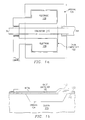
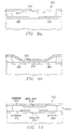
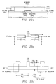
- FIG. 1a-b illustrate in plan and cross sectional elevation views of such switches with silicon dioxide (“oxide") cantilever 102 extending out over 7 Tm-deep opening 104 etched in silicon substrate 106.
- Metal electrodes 108-109 extend onto cantilever 102, and metal conductor 110 extends onto and up and out over the end of cantilever 102.
- Metal contact 120 on oxide 112 lies in the same plane as canitlever 102 and extends out under the end of conductor 110.
- the switch operates as follows.
- cantilever 102 With no voltage applied between electrodes 108-109 and silicon substrate 106, cantilever 102 remains parallel to the surface of silicon substrate 106 and the switch is open. However, about 60 volts applied between the electrodes and the substrate pulls cantilever 102 towards substrate 106 until the end of conductor 110 makes contact with metal 120. This closes the switch. Release of the pull down voltage then opens the switch.
- Micromechanical spatial light modulators with metallized polymer membranes appear in Hornbeck, U.S. Patent No. 4,441,791.
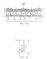
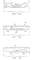
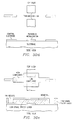
- Figure 2a shows a cross sectional elevation view through two pixels of an array of such pixels
- Figure 2b shows the equivalent circuit.
- Voltage applied between the metal film 30-31 on the underside of polymer membrane 35 and the underlying electrode 21 pulls the membrane part way down to the electrode and thereby disrupts the flat surface of reflecting metal film 26 on the polymer membrane and thereby modulates reflected light. Applying too large a voltage collapses the polymer membrane down to the electrode and destroys the pixel.
- Selectively applying voltages to pixels in the array permits spatial light modulation.
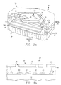
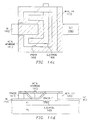
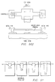
- Figures 3a-d show such a pixel in perspective, cross sectional and plan views with metal beam 30 suspended by thin metal torsion hinges 34 and 36 over underlying electrodes 42 and 46 plus landing pads 40-41. With no voltage applied between electrodes 42, 46 and beam 30, the beam remains parallel to the metal surface 26, 28 as in Figure 3b. A voltage applied between electrode 42 and beam 30 pulls on the beam and the beam twists counterclockwise (in Figure 3d) on hinges 34, 36 and one beam edge moves down toward the electrode while the other beam edge rises as illustrated.
- Beam 30 stops when it contacts landing pad 40, which is at the same voltage as the beam (typically, ground). With beam 30 in this tilted position, light reflects at a different angle from the beam than light reflecting from the surface 28. Removal of the applied voltage allows hinges 34, 36 to relax and return beam 30 to the position parallel to the surface 28. Thus an array of such pixels can act as a spatial light modulator.
- the present invention provides micromechanical microwave switches and arrays of switches with membranes and flaps supported on at least two sides.
- the invention has advantages including switches with no power consumption, low cost, and linearity; and also compatibility with both silicon and gallium arsenide integrated circuits.
- Figures 1a-b show a known micromechanical switch.
- Figures 2a-b illustrate a known polymer spatial light modulator pixel.
- Figure 3a-d are perspective, cross sectional, and plan views of metal torsion beam spatical light modulator pixel.
- Figures 4a-e are plan and cross sectional elevation views of a top side metal membrane preferred embodiment switch.
- Figure 5 shows a preferred embodiment single pole, double throw switch.
- Figure 6 illustrates a preferred embodiment merged pair of SPDT switches.
- Figures 7a-c are plan views of variations of the switch of Figures 4a-e.
- Figures 8a-c are plan and cross sectional elevation views of a dielectric membrane preferred embodiment switch.
- Figures 9a-b are cross sectional elevation views of dielectric membrane with underside metal preferred embodiment switch.
- Figure 10 is a cross sectional elevation view of a dielectric coated version of the preferred embodiment switch of Figures 9a-b.
- Figures 11a-c are plan and cross sectional elevation views of a two-material membrane preferred embodiment switch.
- Figures 12a-d are plan and cross sectional elevation views of a metal membrane preferred embodiment switch.
- Figures 13a-b are cross sectional elevation views of a dielectric-coated microstrip preferred embodiment switch.
- Figures 14a-d are plan and cross sectional elevation views of component membrane preferred embodiment switch.
- Figures 15a-d are variations of the embodiment of Figures 14a-d.
- Figure 16 is a cross sectional elevation view of two-material membrane preferred embodiment.
- Figure 17 is a cross sectional elevation view of another two-material membrane preferred embodiment.
- Figures 18a-e are plan and cross sectional elevatin views of a torsion hinged preferred embodiment.
- Figures 19a-b show a dielectric coated microstrip version of the embodiment of Figures 1 8a-e.
- Figures 20a-c are plan and cross sectional elevatin views of flexure hinged preferred embodiment.
- Figures 21 shows a dielectric coated microstrip version of the embodiment of Figures 20a-c.
- Figure 22 is a cross sectinoal elevation view of a pull up preferred embodiment switch.
- Figures 23a-b are plan and cross sectional elevatin views of a bistable membrane preferred embodiment switch.
- Figure 24 is a cross sectinoal elevation view of a top contact version of the switch of Figures 23a-b.
- Figures 25a-c shows a torsion hinged SPDT and variation.
- Figure 26 shows a membrane SPDT.
- FIGS 27a-b illustrate a membrane SP3T.
- Figures 28a-b show a six output switch and application to a filter.
- Figures 29a-h show shunt switches.
- FIGS 30a-f illustrate fabrication steps.
- Figure 31 shows a swithced line phase shifter.
- Figures 32a-b show quadrature hybrid-coupled time delay phase shifters
- Figure 33 shows a periodically loaded-line phase shifter.
- Figures 34a-c illustrate aperture fill time compensating newtworks.
- Figure 35 shows digital phase scanning
- FIGS 36a-b illustrate Butler matrix beam selection.
- Figure 37 is a 5-beam Blass matrix beam selection.
- Figure 38 shows a 30-beam Rotman lens feeding a 30 element linear array.
- Figure 39 illustrates circular symmetric array beam selection.
- Figure 40 shows a transmit/receive module
- Figure 41 shows filter selectivity tuning.
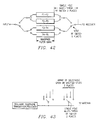
- Figure 42 shows channelizer switching
- Figure 43 illustrates electronic device impedance match tuning.
- Figures 44-45 show dipole and circular patch antenna frequency selectivity tuning.
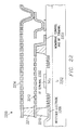
- the preferred embodiment systems use single ones or arrays of preferred embodiment switches for functions such as beam steering in a phased array radar. And the preferred embodiment switches all switch a high frequency electrical signal by deflecting a movable element (conductor or dielectric) into or out of a signal path to open or close either capacitive or ohmic connections.
- Figures 4a-29 illustrate preferred embodiment switches
- Figures 31-45 show preferred embodiment systems incorporating preferred embodiment switches.
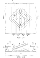
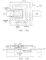
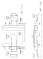
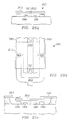
- FIGS 4a-e illustrate first preferred embodiment switch, generally dennoted by reference numeral 400, in plan view and cross sectional elevation views for both open and closed states.
- Switch 400 includes substrate 401 (which may be a silicon dioxide film a few Tm thick on a silicon die) with transmission line microstrip segments 402-403 and control electrodes 405-406 on the substrate surface and within an opening in insulating spacer layer 410 on the substrate surface.
- Dielectric membrane 412 lies on spacer 410 and spans the opening.
- Metal plate 414 and metal film 415 attached to the upper surface of membrane 412 provide the signal conducting and mechanical deflection for the switching action, respectively.
- metal film 415 and electrodes 405-406 form an air gap capacitor which deflects membrane 412 when charged, as follows.
- dielectric membrane 412 is relatively flat as shown in cross setional elevation views Figures 4b-c.
- the gap between microstrip segments 402-403 imposes a large impedance in the transmission line and the switch is open.
- a positive voltage applied between electrodes 405-406 and grounded metal film 415 induces positive electric charges on electrodes 405-406 and negative charges on metal film 415, and these charges generate an attractive force which pulls metal film 415 (and membrane 412) down to electrodes 405-406 as illustrated in Figures 4d-e.
- Dielectric membrane 412 prevents metal film 415 from touching electrodes 405-406, so only leakage current flows during this activation of electrodes 405-406.
- Switch 400 is a single pole-single throw (SPST) switch.
- SPST single pole-single throw
- switch applications such as the transmit/receive module schematically illustrated in Figure 40, frequently require a single pole-double throw (SPDT) switch.
- the preferred embodiment switches include both ohmic and capacitive connections, electrostatic and thermal activation, conducting and dielectric deformable membranes, electrical and mechanical restoring forces, and localized and support element current carrying.
- the materials used for switch fabrication may also be used for fabrication of various transmission line configurations, including microstrip, stripline, coplanar waveguide, and coplanar stripline.
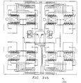
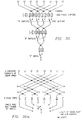
- phase steered aperture 3400 consists of a 5 by 5 array of submodules with each submodule ( Figure 34b) a 4 by 4 array of antenna elements plus a power amplifier for transmit and a low noise amplifier for receive plus a 4-bit phase shifter for each antenna element.
- Each submodule connects to a variable time delay network (labelled ⁇ , 2 ⁇ , ... N ⁇ in Figure 34a for the delays produced) which is a 5-bit switched line time delay as shown in Figure 34c with SPDT switches and binary-weighted-length delay lines.
- ⁇ , 2 ⁇ , ... N ⁇ in Figure 34a for the delays produced
- the total path length can be varied by in increments of D/32 up to a total increase of 31/32 D.
- Each bit of the 5-bit switched line time delay contains a pair of SPDTs that select either of two possible path lengths with path length differentials being D/2 K for the kth bit.
- Figure 34c shows selection of increases of D/32, D/8, and D/4 for a total increase of 13/32 D.
- Each pair of SPDTs could be replaced by a compact layout which uses only three coupling metal plates 601-603 and electrode pairs 611-613 on a single U-shaped membrane as illustrated in Figure 6.
- Activating electrodes 611 only pulls down metal plate 601 to couple the IN microstrip directly to the OUT microstrip; whereas activating electrodes 612-613 and deactivating electrodes 611 disconnects the direct coupling and couples in the delay loop.
- the preferred embodiment systems include phase shifters, time delay networks, beam selectors, trasmit/reeive duplexing, and frequency selectors.
- FIGS. 4a-e show in plan and cross sectional elevation views preferred embodiment capacitive switch 400; note that the vertical dimensions have been greatly exaggerated for clarity.
- the previous section outlined the operation of switch 400 and noted that the signal conducting portion (plate 414) on the membrane is localized in the center of the membrane.
- Microstrip segments 402-403 have a width of about 50-75 Tm, a thickness of about 0.4 Tm (away from the switch structure the microstrip is plated to a thickness of about 5 Tm), and are separated by a gap of about 100-125 Tm.
- Electrodes 405-406 are about 0.4 Tm thick and are spaced about 25 Tm from microstrip segments 402-403.
- Spacer 410 is about 2 Tm thick
- dielectric membrane 412 is about 0.2 Tm thick and made of silicon nitride with adhered metal film 415 about 0.4 Tm thick.
- Membrane 412 and metal film 415 and metal plate 414 include an array of 1 Tm holes spaced about 7 Tm apart which permit plasma etching to remove underlying spacer layer and create the opening in the spacer.
- the drawings omit showing these plasma access holes for clarity. Similarly, other preferred embodiments described in the following have drawings omitting plasma access holes.
- Membrane 412 plus metal film 415 have a total thickness of 0.6 Tm and are quite compliant but also provide sufficient restoring force to pull up after electrodes 405-406 are deactivated.
- the thickness of membrane 412 and metal film 415 provide a tradeoff of the electrode threshold voltage required to pull down and the restoring force required for pull up (to overcome any sticking plus have a small switching time).
- an electrode voltage of about 30 volts suffices; the threshold voltage is a little less.
- Metal plate 414 is about 0.5 Tm thick and about 50-75 Tm wide and 300 Tm long; thus when pulled down onto microstrip segments 402-403, metal plate 414 overlaps about 250 Tm of each segment. With nitride membrane 412 as the capacitor dielectric, metal plate 414 capacitively couples to microstrip segments 402 and 403 with roughly a 5 pF capacitance.
- the 5 pF capacitor presents an impedance of roughly 3 ohms.
- the tension in membrane 412 pulls it up about 2 Tm to be flat and thereby drop the capacitance between metal plate 414 and microstrip segments 402-403 by a factor of roughly 75 due to the change of the dielectric from 0.2 Tm of nitride to 1.8 Tm of air plus 0.2 Tm of nitride.
- the open switch imposes an impedance of roughly 200 ohms in the transmission line at 10 GHz.
- the size of switch 400 metal plate about 600 Tm long
- switch 400 provides a dc block between the microstrips due to the rf capacitive coupling. Indeed, this is true of all of the following switches with capacitive coupling.
- Substrate 401 may be made of various materials. For example, silicon on sapphire, gallium arsenide, alumina, glass, silicon on insulator, etc. Formation of the switch on a thick oxide region on a silicon substrate permits control circuitry for the control electrode, including charge pumps, to be integrated on the same die as the switch. The oxide also helps reduce dielectric losses associated with the silicon substrate.
- spacer 410 may be made of various materials such as photoresist, PMMA, etc., or may be conductive as in some preferred embodiments described in the following and thus made of various metals.
- Membrane 412 may be made of many different dielectrics such as quartz, silicon dioxide, silicon nitride, organic polymers of various types, and high dielectric ferroelectric material such as PLZT, SBN, BST, and GaAs, InP, and layered versions of such materials.
- a leaky dielectric should be used to avoid static charge build up in the dielectric which would act as an activation charge.
- FIGS 7a-c show in plan views variations of switch 400, labelled as 700, 730, and 760, respectively
- Switch 700 has the IN and OUT microstrip segments in the form of interdigitated fingers. This geometry allows for a shorter but wider switch while providing the same capacitive coupling as switch 400.
- Switch 730 has the IN and OUT microstrip segments as side by side which also shortens the switch;
- Figure 7b shows the control electrodes but omits the metal plate and metal film for clarity and indicates two horseshoe-shaped spacers leaving gaps for the microstrip segments.
- Switch 760 has the two electrodes connected between the microstrip segment ends; this provides simple electrode connection plus an rf ground between the microstrip ends to increase isolation.
- Figures 8a-c show switch 800 in cross sectional elevation view along the microstrips and in plan view as similar to switch 400 but with the omission of the metal plate.
- Switch 800 operates by changing the dielectric over and coupling the microstrip segments 802-803 from air to the nitride of membrane 812 and thereby increasing the capacitive coupling by a factor of about 7.
- Trench 820 at least 1-5 Tm deep and 20 Tm long (and at least as wide as the microstrip segments) limits the capacitive coupling through the substrate.
- trench 820 permits microstrip segments 802-803 to be brought closer together, and metal electrode connector 825 may run through trench 820 and provide an rf ground to further lessen the capacitive coupling through the substrate plus simplify connection to electrodes 805-806.
- Grounded metal films 815-816 lie on membrane 812 over electrodes 805-806.
- Figure 8a shows switch 800 open, and Figure 8b shows electrodes 805-806 activated and switch 800 closed.
- Switch 800 relies on the change in dielectric constant from about 1 (air when the switch is open) to the dielectric constant of the membrane (when the switch is closed).
- membrane 812 could be made of a ferroelectric such as PLZT, BST, SBN, and so forth to increase the ratio of off impendance to on impedance.
- switch 400 could have a trench and electrode connector analogous to trench 820 and connector 825
- switch 800 could have interdigitated microstrip segments analogous to switch 700.
- Preferred embodiment switch 400 could be modified to replace the capacitive coupling with an ohmic coupling by placing the metal plate on the underside of the dielectric membrane as illustrated in cross sectional elevation view in Figure 9a-b by switch 900.
- An ohmic coupling permits switching also of dc or low frequency signals.
- metal plate 914 is put on the underside of membrane 912 to provide direct metal-metal contacts with the microstrip segments;
- Figure 9a shows the open postion with metal plate 912 suspended about 2 Tm above microstrip segments 902-903
- Figure 9b shows the switch closed with metal plate 914 bridging microstrip segments 902-903 for ohmic connection.
- ohmic connection switch 900 may be much smaller than switch 400 because the large overlap area of the metal on the microstrip segments for high capacitance coupling is not needed for ohmic coupling.
- the ohmic coupling area must be sufficient to limit the current density to what the contact can support without creating hot spots and welding closed. Thus the dimensions depend upon the application.
- Both metal plate 914 and microstrip segments 902-903 may be gold or gold plated to provide good ohmic contact.
- Figure 10 shows switch 1000 as a variation of switch 900 with metal plate 1014 on the underside of membrane 1012 but with dielectric coatings 1020 on microstrip segments 1002-1003 to provide capacitive coupling.
- a very thin ( ⁇ 0.03 Tm) dielectric layer 1020 can be used on the microstrip segments to increase the capacitive coupling because this dielectric need not have the mechanical strength of the membrane 812 in switch 800.
- high dielectric constant material could be used for the dielectric layer 1020; for example, alumina, PLZT, BST, etc.
- FIGS 11a-b show in plan and cross sectional elevation views preferred embodiment switch 1100 which has metal film 1115 on silicon nitride file 1112 over microstrip segments 1102-1103.
- Switch 1100 differs from switch 400 by having a single metal film 1115 covering the entire membrane rather than a grounded metal film for the pull down electrodes to attract and a separate metal plate for the capacitive coupling of the microstrip segments.
- Grounded metal film 1115 has an inductive connection to ground for rf isolation.
- the use of single metal film 1115 for both the electrode attraction and the capacitive coupling of the microstrip segments provides a tradeoff of simpler fabrication but larger parasitic capacitance.
- Figure 11c heuristically illustrates in plan view an electrodeless version of switch 1100 in that the microstrip segments also provide the dc control voltage for pull down of the metal membrane.
- dc isolation of the portions of the microstrip segments in the switch from the remainder of the microstrip permits use of the microstrip segments themselves as the electrodes.
- the varying rf voltage does not affect switch operation because of the inertia of the membrane.
- the switch can be made narrower and be optimized for higher frequency operation.
- transmission line geometry could be used such a coplanar waveguide with the ground lines running under the spacer.
- Figure 12a shows in cross sectional elevation view preferred embodiment switch 1200 which has metal film membrane 1215 over microstrip segments 1202-1203 which pulls down to create an ohmic connection between the microstrip segments.
- Switch 1200 emulates switch 1100 by having a single grounded metal film 1215 for both the pull down electrodes to attract and for the coupling of the microstrip segments.
- Grounded metal film 1215 also has an inductive connection to ground for rf isolation.
- Metal membrane 1215 may be made of aluminum, gold, titanium-tungsten, or a layered structure such as TiW/Pt/Au.
- Figures 12b-c show in plan and cross sectional elevation views a variation of switch 1200 with a roughly indented rectangular metal membrane 1215 suspended on metal posts 1221-1222 at each short end and with coupled microstrips 1202-1203 entrant at each long end.
- a voltage applied to posts 1221-1222 pulls metal film down towards the grounded substrate and this makes the ohmic contact to the microstrips.
- the portions of metal film 1215 adjacent the posts is narrower than the center portion, so metal film 1215 bends primarily adjacent the posts as illustrated in Figure 12d.
- Figures 13a-b show in cross sectional elevation views preferred embodiment switch 1300 which has metal film membrane 1315 over microstrip segments 1302-1303 which have dielectric coatings 1332-1333.
- Switch 1300 emulates switch 1000 by having a single grounded metal film 1315 for both the pull down electrodes to attract and for the capacitive coupling of the microstrip segments.
- Grounded metal film 1315 also has an inductive connection to ground for rf isolation.
- electrodes 1305-1306 also have dielectric coatings or are recessed below dielectric posts to avoid a short circuit during activation.
- Figure 13b is a cross sectional along a line perpendicular to that of Figure 13a and illustrates the recessed electrodes.
- Figure 13a shows recessed electrode connector 1307 which connects electrodes 1305 and 1306 and also contributes to the isolation of the microstip segments 1302-1303.
- FIGS 14a-b illustrate in plan and cross sectional elevation views preferred embodiment switch 1400 which differs from the previously described switches by connecting one microstrip to the deflectable membrane.
- switch 1400 includes a silicon substrate with a 2 Tm thick silicon dioxide layer 1401 with transmission line microstrip segments 1402-1403 and control electrode 1406 on the surface of oxide 1401 and within an opening in spacer annulus 1410.
- Metal membrane 1412 lies on spacer 1410 and spans the opening and extends down the outside to connect to microstrip 1403.
- Metal membrane provides the rf signal conducting and mechanical deflection for the switching action, respectively.
- metal membrane 1412 and electrode 1406 form an air gap capacitor which deflects membrane 1412 when charged and thereby makes an ohmic connection of microstrip 1402 through membrane 1412 to microstrip 1403.
- Electrode 1406 lies in a recess in oxide 1401, and additionally an array of oxide posts 1430, each about 2 Tm in diameter, project through electrode 1406 with a spacing of about 5 Tm, so metal membrane 1412 will not contact electrode 1406 when the activated electrode pulls the membrane down.
- Annular spacer 1410 has an outside diameter of about 400 Tm, and inside diameter (opening) of about 250 Tm, and a height of about 2 Tm.
- Microstrip 1402 may be narrowed from 50-75 Tm wide to 25 Tm wide to be separated from electrode 1406 but widen again to 50-75 Tm at its circular terminus in the center of the opening; this allows a greater contact area with membrane 1412 and consequently a smaller operating current density.
- Electrode 1406 may lie in a 1 Tm deep recess in oxide 1401. Roughly 30 volts between electrode 1406 and membrane 1412 will pull down the membrane to make contact with the terminus of microstrip 1402.
- Membrane 1412 is made of aluminum and about 0.4 Tm thick; this provides sufficient restoring force to pull the membrane up off of microstrip 1402 and back to horizontal upon deactivation of electrode 1406.
- the dc grounding of membrane 1412 and microstrip 1403 is through a choke to ground (not shown) plus a series capacitor (not shown) to dc isolate the membrane from the remainder of microstrip 1403.
- Figures 14c-d show in plan and cross sectional elevation views a rectangular rather than circular geometry for switch 1400.
- one side of membrane 1412 connects to microstrip 1403 by vertical metal via 1450.
- FIGS 15a-b show in plan and cross sectional elevation views preferred embodiment capacitive switch 1500 which is the same as switch 1400 but with thin ( ⁇ 0.05 Tm) dielectric 1520 coatings on the microstrip segment 1502. This prevents metal membrane 1512 from touching microstrip 1502 and provides capacitive coupling of the microstrips analogous to switches 1000 and 1300.
- Figures 15c-d show in plan and cross sectional elevation views an electrodeless version of switch 1500 which omits the electrode and applies the dc pull down voltage to the dc-isolated portions the microstrips 1502-1503.
- Capacitors 1532-1533 provide the isolation and inductors 1542-1543 provide chokes for application of the pull down dc voltage between the microstrips.
- Figure 16 shows in cross section elevation view switch 1600 which is similar to switch 1400 except the membrane is dielectric membrane 1612 with overlying metal film 1615.
- Dielectric 1612 prevents ohmic contact but provides capacitive coupling of the underlying microstrip through metal film 1615 to microstrip.
- the use of dielectric film 1612 also elininates the need to recess the pull down electrode. Note that Figure 16 shows both the pulled up and the pulled down membrane positions.
- Figure 17 shows in cross section elevation view switch 1700 which is similar to switch 1400 except the membrane is dielectric membrane 1712 with underlying metal film 1715. This provides ohmic contact as in switch 1400 with additional dielectric covering of the membrane.
- FIGS 18a-b illustrate in plan and cross sectional elevation views preferred embodiment switch 1800 which differs from the previously described membrane switches by using stiff metal flap 1812 suspended by two thin metal hinges 1821-1822. This is analogous to the spatial light modulator torsion beam pixel of Figures 3a-d.
- Application of voltage between dc-grounded flap 1812 and electrode 1806 attracts flap 1812 and rotates the flap counterclockwise (in Figure 18b) about an axis through the hinges. This pulls one edge of the flap down to contact microstrips segments 1802-1803 to form an ohmic connection between the microstrips to close the switch.
- Flap 1812 is rf isolated from ground by a choke inductor.
- thick (gold plated) microstrips 1802-1803 imply a small gap between flap 1812 and the microstrips for the case of no applied electrode voltages; thus flap 1812 will have a large area of contact with the microstrips because the flap is still close to parallel to the microstrip surfaces.
- a large area of contact (especially with a soft gold microstrip surface) limits the current density at the contact and extends switch life.
- Metal flap 1812 may be about 200 Tm wide (extending 100 Tm from the rotation axis of the hinges) and fairly thick (5 Tm) to remain somewhat stiff and avoid sagging.
- Hinges 1821-1822 may attach to a surrounding metal layer on a spacer as illustrated in Figures 18c-d or may attach to metal posts (analogous to the switch in Figures 12b-d) or even a series of metal posts as illustrated in Figure 18e.
- Figure 19a shows switch 1900 which includes microstrip dielectric coatings but otherwise is analogous to switch 1800.
- microstrips 1902-1903 have dielectric coatings 1920.
- voltage applied to electrode 1906 rotates flap 1912 about hinges 1921-1922 to pull on an edge of flap 1912 down to contact the microstrips, a capacitive coupling forms.
- Figure 19b shows an alternative capacitive coupling approach by torsion beam 1912 in which microstrips 1902-1903 have a separation of just the length of an edge of beam 1912.
- beam 1912 when beam 1912 is pulled down into the separation space, it capacitively couples to each microstrip and thereby closes the switch.
- switch 2000 which includes rectangular metal flap 2012 suspended by flexure hinges 2021-2024 at each corner; recessed electrodes 2006 and microstrips 2002-2003 run under flap 2012. Flap 2012 is thicker than the hinges and is grounded through an rfchoke. Switch 2000 operates as follows. With no voltage applied between electrodes 2006 and flap 2012, hinges 2021-2024 hold flap 2012 up over microstrips 2002-2003 and the switch is open as in Figure 20b. Conversely, with an applied voltage between the electrodes and the flap, flap 2012 is pulled down to bend the hinges and to make contact with the microstrips and thereby close the switch as in Figure 20c. When the electrode voltage is removed, the hinges relax and pull up the flap to open the switch.
- hinges 2021-2024 may connect to a spacer or to posts.
- Figure 21 illustrates in cross sectional elevation view preferred embodiment switch 2100 which differs from switch 2000 simply by dielectric coatings 2120 on the microstrips 2102/2103 (and on electrodes 2106 to eliminate the need for recesses) for capacitive coupling.
- Hinges 2121-2124 support flap 2112 either by connection to a metal layer on a spacer or to metal posts.
- FIG 22 illustrate in cross sectional elevation views preferred embodiment switch 2200 which is analogous to switch 1400 but with an additional overlying metallized dielectric membrane 2256 which acts as a pull up electrode for metal membrane 2212 which connects to microstrip 2202.
- a voltage applied between recessed electrode 2206 and membrane 2212 pulls the membrane down to make contact with microstrip terminus 2202 and thereby close the switch.
- a voltage applied between overlying membrane 2256 and metal membrane 2212 (while no voltage is applied between underlying electrode 2206 and membrane 2212) pulls membrane 2212 up to open the switch.
- switch 2200 has electrical activation for both switch closing and opening and does not rely exclusively on mechanical restoration for switch opening.
- Figure 22 also shows spacers 2210-2211 and plasma access holes in both of the membranes.
- Switch could be fabricated by first form the underling electrode and microstrips; spin on spacer and form vias; deposit metal and pattern it for membrane 2212 plus a part of the vertical connection for the overlying membrane, this metal deposition also fills the vias to make vertical connections; spin on a second spacer layer and form a via; deposit metal and pattern it to from the overlying electrode membrane; lastly, plasma etch to remove unwanted spacer.
- overlying pull up electrode analogous to membrane 2256 in order to have electrical switch opening.
- the overlying pull up membrane could be supported by posts rather than spacer, so a spacerless switch with electrical pull up can be made. In this case insulation layers between stacked posts will be needed.
- Figures 23a-b illustrate in plan and cross sectional elevation views preferred embodiment switch 2300 which differs from the previously desribed switches by use of stiff bimetal membrane or a film 2315 formed with compressive strain which has two stable states of curvature as illustrated in Figure 23b.
- TiW, silicon dioxide, and silicon nitride can all be easily deposited with compressive strain.
- For a dielectric membrane apply a thin metallic coating on the bottom side.
- One curvature state corresponds to an open switch with the membrane separated from the microstrips (2315 OPEN in Figure 23b), and the second state corresponds to a closed switch with the membrane making an ohmic connection between the microstrips (2315 CLOSED in Figure 23b).
- the states can be toggled by voltage applied either between membrane 2315 and pulldown electrodes 2305-2306 or between membrane 2315 and overlying pullup electrode membrane 2356. Note that once membrane 2315 enters one of the two states, no further voltage need be applied to hold it in the state: there is no mechanical restoration force. And as with other electrodeless switch embodiments, dc isolation plus rf chokes are used for pull up (and pull down if it also is electrodeless) voltage. The use of both pull up and pull down electrodes is analogous to the structure of Figure 22. Compressive strain membrane 2315 is attached to metal vias 2321-2322, so the membrane cannot relax. Fabrication would follow that of switch 1200 using posts, although a spacer version could be made analogous to switch 2200. In either case, the strain membrane must be attached to fixed supports to avoid relaxation of the strain.
- a bimetallic bistable membrane can be toggled between curvature states by thermal cycling using the resistance of the membrane and running a dc current through the membrane.
- the overlying pullup film 2356 may be omitted as well as the pull down electrodes.
- direct laser beam heating may be used for the toggling.
- the membrane length (between support vias) and thickness depend upon the switch size, film strain, and the Euler buckling criterion which states that the film will buckle if the strain exceeds X/3 times the square of the quotient of the thickness divided by the length.
- the strain can be controlled by deposition process parameter adjustments.
- Switch 2300 can be turned into a capacitive coupled switch by applying dielectric coatings on the microstrips, or using a metal coated dielectric membrane.
- dielectric coatings on the microstrips, or using a metal coated dielectric membrane.
- a 1.5 Tm thick silicon membrane with a 0.4 Tm thick aluminum top coating and 400 Tm long by 30 Tm wide could be used.
- Switch 2300 can also be connected analogous to switch 1400 with one microstrip attached to the metal vias which support a metal or metal coated dielectric film and only a single microstrip under the membrane.
- Figure 24 shows switch 2400 as a modification of switch 2300 in which the top pullup electrode membane 2456 makes contact with the compressive strain membrane 2415.
- SPST single pole-single throws
- Figure 5 shows an SPDT made with a single membrane
- Figure 6 shows a merged version of two SPDTs formed with a single membrane
- Figure 24 illustrates an SPDT.
- FIGs 25a-b shows torsion flap SPDT switch 2500 including metal flap 2512 supported by hinges 2521-2522 with electrodes 2505-2506 on either side of the rotation axis of the torsion flap.
- Input on microstrip 2502 goes out either microstrip 2503 or 2504.
- switch 2500 could be modified by an overlying pair of contacts such as illustrated in Figure 25c.
- the torsion flap would be rf isolated and just act as a conduit connecting either microstrip 2502 to overhanging conductor 2552 or microstrip 2503 to overhanging conductor 2553.
- Figure 26 illustrates in plan view SPDT switch 2600 which could be considered an SPDT version of switch 1400.
- Metal memebrane 2612 connects by a via to input microstrip 2602 and extends over recessed pull down electrodes 2605-2606. With a dc pull down voltage between electrode 2605 and membrane 2612 pulls down to make connection with microstrip 2603 and close one switch; conversely, activation of electrode 2606 pulls the membrane down to microstrip 2604 and close the other switch.
- Membrane 2612 could be about 250 Tm wide and 400 Tm long and be suspended about 2 Tm over the microstrips. About 30 volts dc will pull down an aluminum membrane of thickness 0.4 Tm.
- Figures 27a-b illustrate in plan and cross sectional views single pole-three throw (SP3T) switch 2700 made of three adjacent switches analogous to switch 1400 and with a common metal membrane 2712 connected by a via to input microstrip 2701 and three recessed electrodes 2705-2707 and corresponding output microstrips 2702-2704. More output microstrips and pull down electrodes could be included by expanding the square geometry either symmetrically as to a pentagon, hexagon, etc. or linearly as illustrated in the next section.
- SP3T single pole-three throw
- a capacitive coupling version of SP3T switch 2700 may easily be realized by dielectric coatings on the end portions of the three underlying microstrips. And the electrodes could also have dielectric coatings and thereby avoid being recessed.
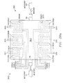
- FIG 28a shows in plan view six throw switch 2800 which could be used in a filter as heuristically illustrated in Figure 28b.
- Switch 2800 includes metal membrane 2812 which spacer 2810 suspends over six output microstrips OUT1-OUT6 and corresponding recessed electrodes.
- Microstrips IN and OUT connect to opposite ends of membrane 2812 by vertical vias, and each includes an inductor to cancel out the excess capacitance of membrane 2812.
- Each electrode pulls down a portion of membrane 2812 to make contact with its corresponding output microstrip.
- membrane 2812 will be dc isolated from the microstrip IN and microstrip OUT to provide the proper dc potential, typically ground.
- the six output microstrips labelled OUT11-OUT6 connect to ground through either lumped or distributed or stub capacitors C1-C3 and inductors L1-L3.
- Figure 29a illustrates heuristically a shunt-series-shunt switch configuration and Figure 29b shows in plan view preferred embodiment 2900 utilizing the foregoing membrane switches.
- metal membrane 2911 pulls down to make the series connection between the IN and OUT microstrips
- metal membrane 2912 pulls down to make both shunt to ground connections for the microstrips.
- Figures 29c-d show in plan and cross sectional elevation views shunt switch 2930 for a coplanar waveguide with ground lines 2940-2941 and center line 2942.
- Vias 2945-2946 suspend metal membrane 2932 about 2 Tm over the centerline and connect the membrane to the ground lines.
- Centerline 2942 is coated with dielectric 2943 and is dc isolated for electrodeless operation.
- a pull down voltage applied to centerline 2942 pulls membrane 2932 down to capacitively couple the centerline to ground.
- Figures 29e-f show a narrow band SPDT switch which uses selective shunting of one of the arms to ground. This avoids off-capacitance problems and uses resonant trensmission lines to achieve proper phaseing.
- the individual shunt to ground switches may each be like switch 2930 or may be combined with a single membrane as illustrated in Figures 29g-h.
- the torsion flap switch 2500 could be used with the flap connected to ground. Also, the foregoing could capacitively couple to ground by dielectric coatings on the microstrips.
- CMOS control logic which are needed away from the area of the switch, and cover these devices with a protective coating.
- Etch to the desired depth e.g., 1 Tm deeper than electrode thickness. See Figure 30a.
- liftoff metal e.g., TiW/Pt/Au roughly 0.4 Tm thick
- microstrips are to be thicker (e.g., 5 Tm) away from the switch, then electroplate them now also recess deeper.
- Spin on the spacer material e.g., 2 Tm of photoresist or polyimide which planarizes the surface. Expose the spacer and develop it to form the via for vertical connection from the evenual metal membrane down to the corresponding microstrip; see Figure 30b. A bake will slope the sidewalls of the spacer for better step coverage.
- deposit the metal film membrane e.g., sputter Al with a thickness 0.4 Tm or low temperature CVD tungsten, this also covers the via sidewalls.
- CMOS complementary metal-oxide-semiconductor
- switches can be integrated with CMOS control circuitry or other logic for driving the electrodes to control the switches.
- the vias could be formed first and then membrane metal and via metal deposited in the same step or as successive steps with a liftoff for the thicker metal on a thinner underlying metal.
- FIG 31 a shows a schematic preferred embodiment four-bit switched line time delay phase shifter.
- Each bit contains two SPDT switches that select either of two possible line length paths.
- the SPDT switches may be any of the prefered embodiment switches; in particular, Figure 6 shows merged SPDTs.
- Figure 32a schematically illustrates a 3-bit quadrature hybrid-coupled time delay phase shifter with preferred embodiment SPST switches.
- a quadrature hybrid coupler has the property that identical reflection coefficients placed on the two 3 dB output ports cause the reflected signals to add constructively at the hybrid isolated port and to add destructively (or cancel) on the hybrid input port. The destructive cancellation at the input port allows the hybrid to maintin its impedance matched property.
- the phase of the resultant constructively added signal at the isolated port has a 1:1 relationship to the phase of the reflection coefficients placed on the hybrid output ports. If unity magnitude reflection coefficients are used, total reflection occurs which results in lossless transmission from the hybrid input port to hybrid isolated port with a phase that is determined by the reflection coefficient phase.
- a similar type phase shifter design in Figure 32b can be realized by using 3-port circulators instead of 3 dB quadrature couplers. Again, the transmitted signal phase of each bit is established by the position of switches on the circulator low-loss output port to reflect the signal to the originally isolated port. The advantage is that each bit requires only one switch to establish the required transmission phase differential.
- a periodically loaded-line phase shifter consists of a transmission line periodically loaded with switched susceptances. Pairs of identical switchable susceptances are spaced approximately one quarter-wavelength apart along the transmission line as shown in Figure 33 with SPST switches to ground; however, a single preferred embodiment multithrow switch as in Figure 28a is used with the microstrip in/out grounded. Reflections from each pair of identical susceptances tend to cancel so that the transmissin line impedance match is maintained. Each pair of switchable suscepatnces produce an increment of the toal desired phase shift diefferenetial. If each susceptance pair produces 22.5 degrees of differential hpase shift, 32 switches would be required to eetablish any phase from 0 to 360 degrees in 22.5 degree increments.
- Figure 34a shows that a signal wavefront incident on an array of length L from an angle 1 off broadside travels a distance of Lsin 1 farther to the last element of the array than it does to the first element.
- T is known as the aperture fill time.
- switchable time-delay networks Figure 34c using preferred embodiment SPDT or merged SPDTs as in Figure 6 can be incorporated behind each element or each subarray of elements of the array.
- Figures 34b shows a 4 by 4 subarray that could be used as a time steered subarray in a phase steered aperture.
- the phase shifters shown are as in Figure 31. If each subarray power amplifier was 16 watts, then each element could receive up to I watt.
- Each element of subarray 3400 is a square patch radiator with side length of approximately 0.350 inch.
- FIG 35 shows a schematic of a digitral phase scanned linear array.
- Each hybrid is a quadrature coupler device and is interconnected with fixed time delay phase shifters and preferred embodiment SPDT rf switches.
- the fixed phase shifters are each multiples of 22.5 degrees (X/8 radians) as shown in the Figure.
- element-to-element phase increments of ⁇ 22.5, ⁇ 67.5, ⁇ 112.5, and ⁇ 157.5 degrees can be achieved.
- Each of these 8 linear element-to-element phase distributions will form a separate beam in space. However, only one beam may be formed at a time.
- Figure 36a shows a schematic of an 8-beam Butler matrix connected to a linerar array of 8 radiating elements.
- the network has 8 beam ports labeled 1 through 4 left and 1 through 4 right.
- Figure 36b shows the 8 array beam patterns generated by the network and are labeled 1 through 4 left and 1 through 4 right.
- a signal received from the diretion of the peak of one of the beams will emerge from the network on the port labeled with the same beam number.
- a signal applied on one of the network beam ports will create the corresponding beam in free space.
- Single pole, multi-throw rf switching on the 8 beam ports allow the individual beams to be selected one at a time.
- Preferred embodiment integrated multithrow switches are used. Multiple switch schemes would allow simultaneous beam forming since all 8 beams can exist at the same time.
- the Blass matrix network will also create simultaneous beams in free space.
- the Blass network can create an arbitrary number of simultaneous beams with an arbitrary number of elements.
- Figure 37 shows a schematic of a 5-beam Blass matrix feeding a linear array of 9 radiating elements.
- the Blass matrix can have a linear length progression from elements 1 through 9 between any two adjacent feedlines of the Figure and park the beams at any arbitrary pointing direction in space. Again, rf switching between the beam ports allows individual beam selection for transmit or receive or multiple beam selection of the simultaneous beams.
- a preferred embodiment integrated multithrow switch is used.
- the Rotman leans is an optical device that focusses the input from several ports of a linear array to a unique point on the rear of the lens. This focussed point is determined by the direction of arrival of the array signal and therefore phase progression of the signals across the linear array. Several beam ports are placed along the back of the lens to collect this focussed energy for each of several possible simultaneous angles of signal arrival.
- Figure 38 shows a schematic of a 30 beam Rotman lens feeding a linear array of 30 radiating elements.
- the many Rotman lens beam ports can be switched to a single receiver or transmitter by a preferred embodiment single pole multi-throw rf switch. Also, multiple switch schemes can allow multiple beams to be selected at the same time from the many simultaneous beams.
- the array of Figure 39 has elements located at a constant interval around the circular antenna.
- An rf manifold is used to create n outputs where n is a subset of the total N elements of the circular array.
- the manifold can have uniform amplitude and phase weighting for maximum effective radiated power or can be amplitude tapered to yield low sidelobe free space patterns.
- the maifold distribution can also be phase-spoiled to give an altered pattern shape.
- a comutating sector of n elements is excited at any one time by rotating rf switching to give 360 degree scan coverage of the pattern, as determined by the manifold.
- Preferred embodiment intgrated single pole multithrow switches are used.
- FIG 40 is a simplified schematic of a transmit/receive module.
- Preferred embodiment SPDT rf switches are used to select either trasnmit or recive capability by connecting the manifold and radiating element ports through the transmit power amplifier (PA) or the receive low noise amplifier (LNA) respectively.
- PA transmit power amplifier
- LNA receive low noise amplifier
- An rf filter is a two port device that selectively passes desired frequencies while reflecting or absorbing unwanted frequencies.
- a reflective filter with a desired passband and stop band is often realized by the accumulation of precise synchronously tuned mismatches spaced along the transmission line connecting input and output ports.
- Figure 41 shows the schematic of a filter in which the synchronously tuned mismatches are stubs (either open or short circuited) that create selective frequency reflections. The frequency selective regions for passband and stopband are determined by the stub spacing, or separation, and stub lengths.
- the desired set of 3 upper or 3 lower stubs in the Figure can be selected for the frequency response as required.
- Preferred embodiment SPST switches provide the connections.
- rf systems are required to be broadband for wide frequency coverage applications.
- some components in the system may be inherently narrow band and cannot cover the full operating bandwidth.
- the wide bandwidth nature of the system may allow unwanted wideband noise to degrade system performance. Therefore, a bank of similar components, each working in its designed narrrow band, may be switched in and out as the frequency is varied to satisfy the full band requirement of the system.
- Figure 42 shows an application of the switching technique to minimize the undesirable noise effect.
- the channelizer is a bank of narrow band bandpass filters each fixed-tuned to contiguous frequency bands across the system bandwidth. As the frequency is varied across the band of operation, the approriate channelizer filter is switched into the receiver path to continuously minimize the noise bandwidth.
- Figure 42 depicts a technique to realize a single pole multi-throw rf switch by using a set of SPDT switches. In either case, preferred embodiment SPDTs or preferred embodiment multithrow switches are used.
- Elecronic devices ranging from hand-held cellular telephones to high power radar transmitters operate in the microwave frequency range and are subject to high frequencvy impedance mismatch problems.
- the matching network required to improve the impedance match may be different under differing operating conditions.
- An example is a hand-held telephone with its antenna in the stowed position versus partially or fully extended or operating inside an aircraft versus a conference room or office. Rf switching can be used to create this needed variable tuning network.
- Figure 43 shows an example of variable tuning the impedance match between the antenna and transmitter/receiver of cellular telephone.
- An array of open or shorted stubs can be selected (either manually or automatically) to continuously improve the impedance match between the two electronic devices. This improved match will increase the signal-to-noise ratio, reduce the required transmit power and prolong operating battery life.
- Preferred embodiment multithrow switches are used, and Figures 28a-b show the case for six elements.
- rf antennas operate at a frequency range that is determined by the radiating element size. By altering the physical dimensions of various antennas, the antenna tuned frequency can be selected.
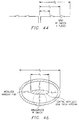
- Figures 44-45 shows two examples of rf switching used to select the antenna size, and therefore, antenna selective tuned frequency.
- Figure 44 shows a dipole antenna whose half-wave resonant length can be selectively chosen as 211, 212, or 213 by the appropriate preferred embodiment rf switch positions.
- the dipole can be tuned to any one of three frequencies. Additional tuned frequencies may be generated by extending the antenna size with additional switches.
- Figure 45 presents a circular patch antenna consisting of the central metallized disk.
- the disk will resonate and, therefore, radiate at a frequency in which the disk diameter, d1, is one-half wavelength.
- d1 the disk diameter
- rf switching to effectively increase the patch antenna diameter to d2
- the antenna will resonate (and radiate) at a different frequency.
- This rf switching may be realized, for example, by a movable (or deformable) metallized annular contact as in switch 1400 that connects the central disk of the Figure to the metallized annular ring.
- Another embodiment of this concept is to let the movable metallized annular contact have an outer diameter of d2, thus eliminating the need for the metallized annular ring in Figure 45.
- the effective patch diameter of the switched combination is d2.
- antenna arrays have very low RCS properties.
- An antenna array that is instantaneously non-operating may reflect and re-radiate unwanted signals as a result of an enemy jammer (for example) illuminating the array.
- enemy detection of the presence of an aircraft of other platform carrying the array may be achieved.
- the antenna array radiating elements in a random manner, the radiation pattern from the array apertaure can be significantly altered or eliminated. Thus, reduction of re-radiated unwanted signals can be achieved.
- Techniques similar to those mentioned in the Antenna Frequency Selectivity Tuning section can be implemented to realize this reconfigurable low RCS antenna array capability. That is, preferred embodiment switches among patches of an array can be open and closed to vary the effective patch sizes.
- the preferred embodiments may be varied in many ways while retaining one or more of the features of micromechanical switching by membranes or flaps supported on at least two sides.
- the dimensions, materials, and voltages can be varied to accommodate switching speed, frequencies of concern, switching control voltage desired, and so forth.
Abstract
Description
- The invention relates to switches for electrical signals, and, more particularly, to switches and systems for high frequency signals with micromechanical switch elements.
- Typical rf switches are p-i-n diodes, but p-i-n diodes have problems including power consumption (the diode must be forward biased to provide carriers for the low impedance state), high cost, and nonlinearity.
- Peterson, Dynamic Micromechanics on Silicon: Techniques and Devices, 25 IEEE Tr.El.Dev. 1241 (1978), includes silicon micromechanical metal-coated cantilevers which act as metal-to-metal switches. Figures 1a-b illustrate in plan and cross sectional elevation views of such switches with silicon dioxide ("oxide")
cantilever 102 extending out over 7 Tm-deep opening 104 etched insilicon substrate 106. Metal electrodes 108-109 extend ontocantilever 102, andmetal conductor 110 extends onto and up and out over the end ofcantilever 102.Metal contact 120 onoxide 112 lies in the same plane ascanitlever 102 and extends out under the end ofconductor 110. The switch operates as follows. With no voltage applied between electrodes 108-109 andsilicon substrate 106,cantilever 102 remains parallel to the surface ofsilicon substrate 106 and the switch is open. However, about 60 volts applied between the electrodes and the substrate pullscantilever 102 towardssubstrate 106 until the end ofconductor 110 makes contact withmetal 120. This closes the switch. Release of the pull down voltage then opens the switch. - Micromechanical spatial light modulators with metallized polymer membranes appear in Hornbeck, U.S. Patent No. 4,441,791. Figure 2a shows a cross sectional elevation view through two pixels of an array of such pixels, and Figure 2b shows the equivalent circuit. Voltage applied between the metal film 30-31 on the underside of
polymer membrane 35 and theunderlying electrode 21 pulls the membrane part way down to the electrode and thereby disrupts the flat surface of reflectingmetal film 26 on the polymer membrane and thereby modulates reflected light. Applying too large a voltage collapses the polymer membrane down to the electrode and destroys the pixel. Selectively applying voltages to pixels in the array permits spatial light modulation. - Spatial light modulators with pixels made of metal torsion beams with landing pads appears in Hornbeck, U.S. Patent No. 5,061,049. Figures 3a-d show such a pixel in perspective, cross sectional and plan views with
metal beam 30 suspended by thinmetal torsion hinges electrodes electrodes beam 30, the beam remains parallel to themetal surface electrode 42 andbeam 30 pulls on the beam and the beam twists counterclockwise (in Figure 3d) onhinges landing pad 40, which is at the same voltage as the beam (typically, ground). Withbeam 30 in this tilted position, light reflects at a different angle from the beam than light reflecting from thesurface 28. Removal of the applied voltage allowshinges beam 30 to the position parallel to thesurface 28. Thus an array of such pixels can act as a spatial light modulator. - Further, applying a voltage between
electrode 46 and beam 30 (and no voltage betweenelectrode 42 and beam 30) will analogously twistbeam 30 in the clockwise direction until it makes contact withlanding pad 41. This provides a second angle of reflection for incident light. - The present invention provides micromechanical microwave switches and arrays of switches with membranes and flaps supported on at least two sides.
- The invention has advantages including switches with no power consumption, low cost, and linearity; and also compatibility with both silicon and gallium arsenide integrated circuits.
- The drawings are schematic for clarity.
- Figures 1a-b show a known micromechanical switch.
- Figures 2a-b illustrate a known polymer spatial light modulator pixel.
- Figure 3a-d are perspective, cross sectional, and plan views of metal torsion beam spatical light modulator pixel.
- Figures 4a-e are plan and cross sectional elevation views of a top side metal membrane preferred embodiment switch.
- Figure 5 shows a preferred embodiment single pole, double throw switch.
- Figure 6 illustrates a preferred embodiment merged pair of SPDT switches.
- Figures 7a-c are plan views of variations of the switch of Figures 4a-e.
- Figures 8a-c are plan and cross sectional elevation views of a dielectric membrane preferred embodiment switch.
- Figures 9a-b are cross sectional elevation views of dielectric membrane with underside metal preferred embodiment switch.
- Figure 10 is a cross sectional elevation view of a dielectric coated version of the preferred embodiment switch of Figures 9a-b.
- Figures 11a-c are plan and cross sectional elevation views of a two-material membrane preferred embodiment switch.
- Figures 12a-d are plan and cross sectional elevation views of a metal membrane preferred embodiment switch.
- Figures 13a-b are cross sectional elevation views of a dielectric-coated microstrip preferred embodiment switch.
- Figures 14a-d are plan and cross sectional elevation views of component membrane preferred embodiment switch.
- Figures 15a-d are variations of the embodiment of Figures 14a-d.
- Figure 16 is a cross sectional elevation view of two-material membrane preferred embodiment.
- Figure 17 is a cross sectional elevation view of another two-material membrane preferred embodiment.
- Figures 18a-e are plan and cross sectional elevatin views of a torsion hinged preferred embodiment.
- Figures 19a-b show a dielectric coated microstrip version of the embodiment of Figures 1 8a-e.
- Figures 20a-c are plan and cross sectional elevatin views of flexure hinged preferred embodiment.
- Figures 21 shows a dielectric coated microstrip version of the embodiment of Figures 20a-c.
- Figure 22 is a cross sectinoal elevation view of a pull up preferred embodiment switch.
- Figures 23a-b are plan and cross sectional elevatin views of a bistable membrane preferred embodiment switch.
- Figure 24 is a cross sectinoal elevation view of a top contact version of the switch of Figures 23a-b.
- Figures 25a-c shows a torsion hinged SPDT and variation.
- Figure 26 shows a membrane SPDT.
- Figures 27a-b illustrate a membrane SP3T.
- Figures 28a-b show a six output switch and application to a filter.
- Figures 29a-h show shunt switches.
- Figures 30a-f illustrate fabrication steps.
- Figure 31 shows a swithced line phase shifter.
- Figures 32a-b show quadrature hybrid-coupled time delay phase shifters
- Figure 33 shows a periodically loaded-line phase shifter.
- Figures 34a-c illustrate aperture fill time compensating newtworks.
- Figure 35 shows digital phase scanning.
- Figures 36a-b illustrate Butler matrix beam selection.
- Figure 37 is a 5-beam Blass matrix beam selection.
- Figure 38 shows a 30-beam Rotman lens feeding a 30 element linear array.
- Figure 39 illustrates circular symmetric array beam selection.
- Figure 40 shows a transmit/receive module
- Figure 41 shows filter selectivity tuning.
- Figure 42 shows channelizer switching.
- Figure 43 illustrates electronic device impedance match tuning.
- Figures 44-45 show dipole and circular patch antenna frequency selectivity tuning.
- The preferred embodiment systems use single ones or arrays of preferred embodiment switches for functions such as beam steering in a phased array radar. And the preferred embodiment switches all switch a high frequency electrical signal by deflecting a movable element (conductor or dielectric) into or out of a signal path to open or close either capacitive or ohmic connections. Figures 4a-29 illustrate preferred embodiment switches, and Figures 31-45 show preferred embodiment systems incorporating preferred embodiment switches.
- For example, Figures 4a-e illustrate first preferred embodiment switch, generally dennoted by reference numeral 400, in plan view and cross sectional elevation views for both open and closed states. Switch 400 includes substrate 401 (which may be a silicon dioxide film a few Tm thick on a silicon die) with transmission line microstrip segments 402-403 and control electrodes 405-406 on the substrate surface and within an opening in insulating
spacer layer 410 on the substrate surface.Dielectric membrane 412 lies onspacer 410 and spans the opening.Metal plate 414 andmetal film 415 attached to the upper surface ofmembrane 412 provide the signal conducting and mechanical deflection for the switching action, respectively. Indeed,metal film 415 and electrodes 405-406 form an air gap capacitor which deflectsmembrane 412 when charged, as follows. First, withmetal film 415 grounded and electrodes 405-406 also grounded,dielectric membrane 412 is relatively flat as shown in cross setional elevation views Figures 4b-c. In this situation, the gap between microstrip segments 402-403 imposes a large impedance in the transmission line and the switch is open. Conversely, a positive voltage applied between electrodes 405-406 and groundedmetal film 415 induces positive electric charges on electrodes 405-406 and negative charges onmetal film 415, and these charges generate an attractive force which pulls metal film 415 (and membrane 412) down to electrodes 405-406 as illustrated in Figures 4d-e.Dielectric membrane 412 preventsmetal film 415 from touching electrodes 405-406, so only leakage current flows during this activation of electrodes 405-406. Also as illustrated in Figures 4d-e, the pulling down ofmetal film 415 plusmembrane 412 movesmetal plate 414 down to bridge microstrip segments 402-403 and provide capacitive coupling of the segments. Hence, the high impedance in the transmission line has been replaced with a low impedance, and the switch is closed. Switch 400 pulls down or restores up in roughly a microsecond; the timing is a tradeoff with pull down voltage: higher electrode voltage implies faster pull down, and stiffer membranes imply faster restoring but require higher voltage for pull down. - Switch 400 is a single pole-single throw (SPST) switch. However, switch applications, such as the transmit/receive module schematically illustrated in Figure 40, frequently require a single pole-double throw (SPDT) switch. Integrating two switches 400 in parallel as shown in plan view in Figure 5 provides the double throw in a compact structure: a single metal film and membrane spanning both openings in the spacer can be used.
- The preferred embodiment switches include both ohmic and capacitive connections, electrostatic and thermal activation, conducting and dielectric deformable membranes, electrical and mechanical restoring forces, and localized and support element current carrying. The materials used for switch fabrication may also be used for fabrication of various transmission line configurations, including microstrip, stripline, coplanar waveguide, and coplanar stripline.
- The preferred embodiment systems include both single switches as in the transmit/receive module of Figure 40 and arrays of switches as in the time steered subarrays of a phase steered
aperture 3400 illustrated in Figures 34a-c. Phase steeredaperture 3400 consists of a 5 by 5 array of submodules with each submodule (Figure 34b) a 4 by 4 array of antenna elements plus a power amplifier for transmit and a low noise amplifier for receive plus a 4-bit phase shifter for each antenna element. Each submodule connects to a variable time delay network (labelled \, 2\, ... N\ in Figure 34a for the delays produced) which is a 5-bit switched line time delay as shown in Figure 34c with SPDT switches and binary-weighted-length delay lines. Thus the total resolution of phase steeredaperture 3400 is 9 bits. - In Figure 34c the total path length can be varied by in increments of D/32 up to a total increase of 31/32 D. Each bit of the 5-bit switched line time delay contains a pair of SPDTs that select either of two possible path lengths with path length differentials being D/2K for the kth bit. Figure 34c shows selection of increases of D/32, D/8, and D/4 for a total increase of 13/32 D. Each pair of SPDTs could be replaced by a compact layout which uses only three coupling metal plates 601-603 and electrode pairs 611-613 on a single U-shaped membrane as illustrated in Figure 6. Activating
electrodes 611 only pulls downmetal plate 601 to couple the IN microstrip directly to the OUT microstrip; whereas activating electrodes 612-613 and deactivatingelectrodes 611 disconnects the direct coupling and couples in the delay loop. - The preferred embodiment systems include phase shifters, time delay networks, beam selectors, trasmit/reeive duplexing, and frequency selectors.
- The following sections provide details as to these switches and systems plus variations of them.
- Figure 4a-e show in plan and cross sectional elevation views preferred embodiment capacitive switch 400; note that the vertical dimensions have been greatly exaggerated for clarity. The previous section outlined the operation of switch 400 and noted that the signal conducting portion (plate 414) on the membrane is localized in the center of the membrane. Microstrip segments 402-403 have a width of about 50-75 Tm, a thickness of about 0.4 Tm (away from the switch structure the microstrip is plated to a thickness of about 5 Tm), and are separated by a gap of about 100-125 Tm. Electrodes 405-406 are about 0.4 Tm thick and are spaced about 25 Tm from microstrip segments 402-403.
Spacer 410 is about 2 Tm thick, anddielectric membrane 412 is about 0.2 Tm thick and made of silicon nitride with adheredmetal film 415 about 0.4 Tm thick.Membrane 412 andmetal film 415 andmetal plate 414 include an array of 1 Tm holes spaced about 7 Tm apart which permit plasma etching to remove underlying spacer layer and create the opening in the spacer. The drawings omit showing these plasma access holes for clarity. Similarly, other preferred embodiments described in the following have drawings omitting plasma access holes. -
Membrane 412 plusmetal film 415 have a total thickness of 0.6 Tm and are quite compliant but also provide sufficient restoring force to pull up after electrodes 405-406 are deactivated. - Indeed, the thickness of
membrane 412 andmetal film 415 provide a tradeoff of the electrode threshold voltage required to pull down and the restoring force required for pull up (to overcome any sticking plus have a small switching time). For switch 400 an electrode voltage of about 30 volts suffices; the threshold voltage is a little less.Metal plate 414 is about 0.5 Tm thick and about 50-75 Tm wide and 300 Tm long; thus when pulled down onto microstrip segments 402-403,metal plate 414 overlaps about 250 Tm of each segment. Withnitride membrane 412 as the capacitor dielectric,metal plate 414 capacitively couples to microstripsegments metal film 415, the tension inmembrane 412 pulls it up about 2 Tm to be flat and thereby drop the capacitance betweenmetal plate 414 and microstrip segments 402-403 by a factor of roughly 75 due to the change of the dielectric from 0.2 Tm of nitride to 1.8 Tm of air plus 0.2 Tm of nitride. Thus the open switch imposes an impedance of roughly 200 ohms in the transmission line at 10 GHz. Note that the size of switch 400 (metal plate about 600 Tm long) is small compared to the signal wavelength at 10 GHz (3 cm in free space and roughly 1 cm for the microstrip over a material with effective dielectric constant of 10). - Also, switch 400 provides a dc block between the microstrips due to the rf capacitive coupling. Indeed, this is true of all of the following switches with capacitive coupling.
-
Substrate 401 may be made of various materials. For example, silicon on sapphire, gallium arsenide, alumina, glass, silicon on insulator, etc. Formation of the switch on a thick oxide region on a silicon substrate permits control circuitry for the control electrode, including charge pumps, to be integrated on the same die as the switch. The oxide also helps reduce dielectric losses associated with the silicon substrate. Similarly,spacer 410 may be made of various materials such as photoresist, PMMA, etc., or may be conductive as in some preferred embodiments described in the following and thus made of various metals. -
Membrane 412 may be made of many different dielectrics such as quartz, silicon dioxide, silicon nitride, organic polymers of various types, and high dielectric ferroelectric material such as PLZT, SBN, BST, and GaAs, InP, and layered versions of such materials. However, a leaky dielectric should be used to avoid static charge build up in the dielectric which would act as an activation charge. - Figures 7a-c show in plan views variations of switch 400, labelled as 700, 730, and 760, respectively,
Switch 700 has the IN and OUT microstrip segments in the form of interdigitated fingers. This geometry allows for a shorter but wider switch while providing the same capacitive coupling as switch 400.Switch 730 has the IN and OUT microstrip segments as side by side which also shortens the switch; Figure 7b shows the control electrodes but omits the metal plate and metal film for clarity and indicates two horseshoe-shaped spacers leaving gaps for the microstrip segments.Switch 760 has the two electrodes connected between the microstrip segment ends; this provides simple electrode connection plus an rf ground between the microstrip ends to increase isolation. - Figures 8a-
c show switch 800 in cross sectional elevation view along the microstrips and in plan view as similar to switch 400 but with the omission of the metal plate.Switch 800 operates by changing the dielectric over and coupling the microstrip segments 802-803 from air to the nitride ofmembrane 812 and thereby increasing the capacitive coupling by a factor of about 7. Trench 820 at least 1-5 Tm deep and 20 Tm long (and at least as wide as the microstrip segments) limits the capacitive coupling through the substrate. Also, trench 820 permits microstrip segments 802-803 to be brought closer together, andmetal electrode connector 825 may run throughtrench 820 and provide an rf ground to further lessen the capacitive coupling through the substrate plus simplify connection to electrodes 805-806. Grounded metal films 815-816 lie onmembrane 812 over electrodes 805-806. Figure 8a showsswitch 800 open, and Figure 8b shows electrodes 805-806 activated and switch 800 closed. -
Switch 800 relies on the change in dielectric constant from about 1 (air when the switch is open) to the dielectric constant of the membrane (when the switch is closed). Thusmembrane 812 could be made of a ferroelectric such as PLZT, BST, SBN, and so forth to increase the ratio of off impendance to on impedance. - Of course, switch 400 could have a trench and electrode connector analogous to trench 820 and
connector 825, and switch 800 could have interdigitated microstrip segments analogous to switch 700. - Preferred embodiment switch 400 could be modified to replace the capacitive coupling with an ohmic coupling by placing the metal plate on the underside of the dielectric membrane as illustrated in cross sectional elevation view in Figure 9a-b by
switch 900. An ohmic coupling permits switching also of dc or low frequency signals. Basically,metal plate 914 is put on the underside ofmembrane 912 to provide direct metal-metal contacts with the microstrip segments; Figure 9a shows the open postion withmetal plate 912 suspended about 2 Tm above microstrip segments 902-903, and Figure 9b shows the switch closed withmetal plate 914 bridging microstrip segments 902-903 for ohmic connection. Withohmic connection switch 900 may be much smaller than switch 400 because the large overlap area of the metal on the microstrip segments for high capacitance coupling is not needed for ohmic coupling. However, the ohmic coupling area must be sufficient to limit the current density to what the contact can support without creating hot spots and welding closed. Thus the dimensions depend upon the application. Bothmetal plate 914 and microstrip segments 902-903 may be gold or gold plated to provide good ohmic contact. - Figure 10 shows switch 1000 as a variation of
switch 900 withmetal plate 1014 on the underside ofmembrane 1012 but withdielectric coatings 1020 on microstrip segments 1002-1003 to provide capacitive coupling. A very thin (< 0.03 Tm)dielectric layer 1020 can be used on the microstrip segments to increase the capacitive coupling because this dielectric need not have the mechanical strength of themembrane 812 inswitch 800. Also, high dielectric constant material could be used for thedielectric layer 1020; for example, alumina, PLZT, BST, etc. - Figures 11a-b show in plan and cross sectional elevation views preferred
embodiment switch 1100 which hasmetal film 1115 onsilicon nitride file 1112 over microstrip segments 1102-1103.Switch 1100 differs from switch 400 by having asingle metal film 1115 covering the entire membrane rather than a grounded metal film for the pull down electrodes to attract and a separate metal plate for the capacitive coupling of the microstrip segments. Groundedmetal film 1115 has an inductive connection to ground for rf isolation. The use ofsingle metal film 1115 for both the electrode attraction and the capacitive coupling of the microstrip segments provides a tradeoff of simpler fabrication but larger parasitic capacitance. - Figure 11c heuristically illustrates in plan view an electrodeless version of
switch 1100 in that the microstrip segments also provide the dc control voltage for pull down of the metal membrane. In particular, dc isolation of the portions of the microstrip segments in the switch from the remainder of the microstrip (by series capacitors and dc control voltage through chokes) permits use of the microstrip segments themselves as the electrodes. The varying rf voltage does not affect switch operation because of the inertia of the membrane. Thus the switch can be made narrower and be optimized for higher frequency operation. - Other transmission line geometry could be used such a coplanar waveguide with the ground lines running under the spacer.
- Figure 12a shows in cross sectional elevation view preferred
embodiment switch 1200 which hasmetal film membrane 1215 over microstrip segments 1202-1203 which pulls down to create an ohmic connection between the microstrip segments.Switch 1200 emulatesswitch 1100 by having a single groundedmetal film 1215 for both the pull down electrodes to attract and for the coupling of the microstrip segments. Groundedmetal film 1215 also has an inductive connection to ground for rf isolation. -
Metal membrane 1215 may be made of aluminum, gold, titanium-tungsten, or a layered structure such as TiW/Pt/Au. - Figures 12b-c show in plan and cross sectional elevation views a variation of
switch 1200 with a roughly indentedrectangular metal membrane 1215 suspended on metal posts 1221-1222 at each short end and with coupled microstrips 1202-1203 entrant at each long end. A voltage applied to posts 1221-1222 pulls metal film down towards the grounded substrate and this makes the ohmic contact to the microstrips. The portions ofmetal film 1215 adjacent the posts is narrower than the center portion, sometal film 1215 bends primarily adjacent the posts as illustrated in Figure 12d. - Figures 13a-b show in cross sectional elevation views preferred
embodiment switch 1300 which hasmetal film membrane 1315 over microstrip segments 1302-1303 which have dielectric coatings 1332-1333.Switch 1300 emulatesswitch 1000 by having a single groundedmetal film 1315 for both the pull down electrodes to attract and for the capacitive coupling of the microstrip segments. Groundedmetal film 1315 also has an inductive connection to ground for rf isolation. Further, electrodes 1305-1306 also have dielectric coatings or are recessed below dielectric posts to avoid a short circuit during activation. - Figure 13b is a cross sectional along a line perpendicular to that of Figure 13a and illustrates the recessed electrodes. Figure 13a shows recessed
electrode connector 1307 which connectselectrodes - Figures 14a-b illustrate in plan and cross sectional elevation views preferred
embodiment switch 1400 which differs from the previously described switches by connecting one microstrip to the deflectable membrane. In particular,switch 1400 includes a silicon substrate with a 2 Tm thicksilicon dioxide layer 1401 with transmission line microstrip segments 1402-1403 andcontrol electrode 1406 on the surface ofoxide 1401 and within an opening inspacer annulus 1410.Metal membrane 1412 lies onspacer 1410 and spans the opening and extends down the outside to connect tomicrostrip 1403. Metal membrane provides the rf signal conducting and mechanical deflection for the switching action, respectively. As withswitch 1200metal membrane 1412 andelectrode 1406 form an air gap capacitor which deflectsmembrane 1412 when charged and thereby makes an ohmic connection ofmicrostrip 1402 throughmembrane 1412 tomicrostrip 1403. -
Electrode 1406 lies in a recess inoxide 1401, and additionally an array ofoxide posts 1430, each about 2 Tm in diameter, project throughelectrode 1406 with a spacing of about 5 Tm, sometal membrane 1412 will not contactelectrode 1406 when the activated electrode pulls the membrane down. -
Annular spacer 1410 has an outside diameter of about 400 Tm, and inside diameter (opening) of about 250 Tm, and a height of about 2 Tm.Microstrip 1402 may be narrowed from 50-75 Tm wide to 25 Tm wide to be separated fromelectrode 1406 but widen again to 50-75 Tm at its circular terminus in the center of the opening; this allows a greater contact area withmembrane 1412 and consequently a smaller operating current density.Electrode 1406 may lie in a 1 Tm deep recess inoxide 1401. Roughly 30 volts betweenelectrode 1406 andmembrane 1412 will pull down the membrane to make contact with the terminus ofmicrostrip 1402.Membrane 1412 is made of aluminum and about 0.4 Tm thick; this provides sufficient restoring force to pull the membrane up off ofmicrostrip 1402 and back to horizontal upon deactivation ofelectrode 1406. Of course, the dc grounding ofmembrane 1412 andmicrostrip 1403 is through a choke to ground (not shown) plus a series capacitor (not shown) to dc isolate the membrane from the remainder ofmicrostrip 1403. - Figures 14c-d show in plan and cross sectional elevation views a rectangular rather than circular geometry for
switch 1400. In this rectangular version, one side ofmembrane 1412 connects to microstrip 1403 by vertical metal via 1450. - Figures 15a-b show in plan and cross sectional elevation views preferred
embodiment capacitive switch 1500 which is the same asswitch 1400 but with thin (< 0.05 Tm) dielectric 1520 coatings on themicrostrip segment 1502. This preventsmetal membrane 1512 from touchingmicrostrip 1502 and provides capacitive coupling of the microstrips analogous toswitches - Figures 15c-d show in plan and cross sectional elevation views an electrodeless version of
switch 1500 which omits the electrode and applies the dc pull down voltage to the dc-isolated portions the microstrips 1502-1503. Capacitors 1532-1533 provide the isolation and inductors 1542-1543 provide chokes for application of the pull down dc voltage between the microstrips. - Figure 16 shows in cross section
elevation view switch 1600 which is similar to switch 1400 except the membrane isdielectric membrane 1612 with overlyingmetal film 1615. Dielectric 1612 prevents ohmic contact but provides capacitive coupling of the underlying microstrip throughmetal film 1615 to microstrip. The use ofdielectric film 1612 also elininates the need to recess the pull down electrode. Note that Figure 16 shows both the pulled up and the pulled down membrane positions. - Figure 17 shows in cross section
elevation view switch 1700 which is similar to switch 1400 except the membrane is dielectric membrane 1712 withunderlying metal film 1715. This provides ohmic contact as inswitch 1400 with additional dielectric covering of the membrane. - Figures 18a-b illustrate in plan and cross sectional elevation views preferred embodiment switch 1800 which differs from the previously described membrane switches by using
stiff metal flap 1812 suspended by two thin metal hinges 1821-1822. This is analogous to the spatial light modulator torsion beam pixel of Figures 3a-d. Application of voltage between dc-groundedflap 1812 andelectrode 1806 attractsflap 1812 and rotates the flap counterclockwise (in Figure 18b) about an axis through the hinges. This pulls one edge of the flap down to contact microstrips segments 1802-1803 to form an ohmic connection between the microstrips to close the switch.Flap 1812 is rf isolated from ground by a choke inductor. Removal of the applied voltage allows the twisted hinges to relax andreturn flap 1812 to parallel to the substrate surface as in Figure 18b and thereby open the switch. Contrarily, a voltage applied toelectrode 1805 twists hinges clockwise and moves the opposite edge ofmetal flap 1812 towardlanding pad 1807 to further open the switch. Thus by applying a voltage toelectrode 1805 at the same time that the pull down voltage onelectrode 1806 is removed provides an electric opening of the switch rather than just relying on the relaxing of the twisted hinges alone. Indeed, thick (gold plated) microstrips 1802-1803 imply a small gap betweenflap 1812 and the microstrips for the case of no applied electrode voltages; thusflap 1812 will have a large area of contact with the microstrips because the flap is still close to parallel to the microstrip surfaces. A large area of contact (especially with a soft gold microstrip surface) limits the current density at the contact and extends switch life. -
Metal flap 1812 may be about 200 Tm wide (extending 100 Tm from the rotation axis of the hinges) and fairly thick (5 Tm) to remain somewhat stiff and avoid sagging. Hinges 1821-1822 may attach to a surrounding metal layer on a spacer as illustrated in Figures 18c-d or may attach to metal posts (analogous to the switch in Figures 12b-d) or even a series of metal posts as illustrated in Figure 18e. - Figure 19a shows switch 1900 which includes microstrip dielectric coatings but otherwise is analogous to switch 1800. In particular, microstrips 1902-1903 have
dielectric coatings 1920. Thus, when voltage applied toelectrode 1906 rotatesflap 1912 about hinges 1921-1922 to pull on an edge offlap 1912 down to contact the microstrips, a capacitive coupling forms. - Figure 19b shows an alternative capacitive coupling approach by
torsion beam 1912 in which microstrips 1902-1903 have a separation of just the length of an edge ofbeam 1912. Thus whenbeam 1912 is pulled down into the separation space, it capacitively couples to each microstrip and thereby closes the switch. -
embodiment switch 2000 which includesrectangular metal flap 2012 suspended by flexure hinges 2021-2024 at each corner; recessedelectrodes 2006 and microstrips 2002-2003 run underflap 2012.Flap 2012 is thicker than the hinges and is grounded through an rfchoke.Switch 2000 operates as follows. With no voltage applied betweenelectrodes 2006 andflap 2012, hinges 2021-2024hold flap 2012 up over microstrips 2002-2003 and the switch is open as in Figure 20b. Conversely, with an applied voltage between the electrodes and the flap,flap 2012 is pulled down to bend the hinges and to make contact with the microstrips and thereby close the switch as in Figure 20c. When the electrode voltage is removed, the hinges relax and pull up the flap to open the switch. - Analogous to the hinges in switch 1800, hinges 2021-2024 may connect to a spacer or to posts.
- Figure 21 illustrates in cross sectional elevation view preferred
embodiment switch 2100 which differs fromswitch 2000 simply bydielectric coatings 2120 on the microstrips 2102/2103 (and onelectrodes 2106 to eliminate the need for recesses) for capacitive coupling. Hinges 2121-2124support flap 2112 either by connection to a metal layer on a spacer or to metal posts. - Figure 22 illustrate in cross sectional elevation views preferred
embodiment switch 2200 which is analogous to switch 1400 but with an additional overlying metallizeddielectric membrane 2256 which acts as a pull up electrode formetal membrane 2212 which connects tomicrostrip 2202. As withswitch 1400, a voltage applied between recessedelectrode 2206 andmembrane 2212 pulls the membrane down to make contact withmicrostrip terminus 2202 and thereby close the switch. Conversely, a voltage applied betweenoverlying membrane 2256 and metal membrane 2212 (while no voltage is applied betweenunderlying electrode 2206 and membrane 2212) pullsmembrane 2212 up to open the switch. Thus analogous to switches 1800-1900,switch 2200 has electrical activation for both switch closing and opening and does not rely exclusively on mechanical restoration for switch opening. - Figure 22 also shows spacers 2210-2211 and plasma access holes in both of the membranes. Switch could be fabricated by first form the underling electrode and microstrips; spin on spacer and form vias; deposit metal and pattern it for
membrane 2212 plus a part of the vertical connection for the overlying membrane, this metal deposition also fills the vias to make vertical connections; spin on a second spacer layer and form a via; deposit metal and pattern it to from the overlying electrode membrane; lastly, plasma etch to remove unwanted spacer. - Other embodiments previously described may also have an overlying pull up electrode analogous to
membrane 2256 in order to have electrical switch opening. The overlying pull up membrane could be supported by posts rather than spacer, so a spacerless switch with electrical pull up can be made. In this case insulation layers between stacked posts will be needed. - Figures 23a-b illustrate in plan and cross sectional elevation views preferred
embodiment switch 2300 which differs from the previously desribed switches by use of stiff bimetal membrane or afilm 2315 formed with compressive strain which has two stable states of curvature as illustrated in Figure 23b. TiW, silicon dioxide, and silicon nitride can all be easily deposited with compressive strain. For a dielectric membrane, apply a thin metallic coating on the bottom side. One curvature state corresponds to an open switch with the membrane separated from the microstrips (2315 OPEN in Figure 23b), and the second state corresponds to a closed switch with the membrane making an ohmic connection between the microstrips (2315 CLOSED in Figure 23b). The states can be toggled by voltage applied either betweenmembrane 2315 and pulldown electrodes 2305-2306 or betweenmembrane 2315 and overlyingpullup electrode membrane 2356. Note that oncemembrane 2315 enters one of the two states, no further voltage need be applied to hold it in the state: there is no mechanical restoration force. And as with other electrodeless switch embodiments, dc isolation plus rf chokes are used for pull up (and pull down if it also is electrodeless) voltage. The use of both pull up and pull down electrodes is analogous to the structure of Figure 22.Compressive strain membrane 2315 is attached to metal vias 2321-2322, so the membrane cannot relax. Fabrication would follow that ofswitch 1200 using posts, although a spacer version could be made analogous to switch 2200. In either case, the strain membrane must be attached to fixed supports to avoid relaxation of the strain. - Alternatively, a bimetallic bistable membrane can be toggled between curvature states by thermal cycling using the resistance of the membrane and running a dc current through the membrane. In this case the
overlying pullup film 2356 may be omitted as well as the pull down electrodes. Further, direct laser beam heating may be used for the toggling. - The membrane length (between support vias) and thickness depend upon the switch size, film strain, and the Euler buckling criterion which states that the film will buckle if the strain exceeds X/3 times the square of the quotient of the thickness divided by the length. The strain can be controlled by deposition process parameter adjustments.
-
Switch 2300 can be turned into a capacitive coupled switch by applying dielectric coatings on the microstrips, or using a metal coated dielectric membrane. In particular, a 1.5 Tm thick silicon membrane with a 0.4 Tm thick aluminum top coating and 400 Tm long by 30 Tm wide could be used. -
Switch 2300 can also be connected analogous to switch 1400 with one microstrip attached to the metal vias which support a metal or metal coated dielectric film and only a single microstrip under the membrane. - Figure 24 shows switch 2400 as a modification of
switch 2300 in which the toppullup electrode membane 2456 makes contact with thecompressive strain membrane 2415. This permits a third microstrip to be connected to the pullup membane vias and form an intrinsic SPDT. That is, an input microstrip connected to strainmembrane 2415 will either connect to afirst output microstrip 2302 whenmembrane 2415 is down or connect to a second output microstrip throughtop membrane 2456 whenmembrane 2415 is up. - Almost all of the foregoing preferred embodiments are single pole-single throws (SPST) switches. However, these switches also provide the foundations for more involved switches which find wide application.
- Figure 5 shows an SPDT made with a single membrane, and Figure 6 shows a merged version of two SPDTs formed with a single membrane. Similarly, Figure 24 illustrates an SPDT.
- Figures 25a-b shows torsion
flap SPDT switch 2500 includingmetal flap 2512 supported by hinges 2521-2522 with electrodes 2505-2506 on either side of the rotation axis of the torsion flap. Input onmicrostrip 2502 goes out eithermicrostrip switch 2500 could be modified by an overlying pair of contacts such as illustrated in Figure 25c. In this case the torsion flap would be rf isolated and just act as a conduit connecting eithermicrostrip 2502 to overhangingconductor 2552 ormicrostrip 2503 to overhangingconductor 2553. - Figure 26 illustrates in plan view SPDT switch 2600 which could be considered an SPDT version of
switch 1400.Metal memebrane 2612 connects by a via toinput microstrip 2602 and extends over recessed pull down electrodes 2605-2606. With a dc pull down voltage betweenelectrode 2605 andmembrane 2612 pulls down to make connection withmicrostrip 2603 and close one switch; conversely, activation ofelectrode 2606 pulls the membrane down tomicrostrip 2604 and close the other switch.Membrane 2612 could be about 250 Tm wide and 400 Tm long and be suspended about 2 Tm over the microstrips. About 30 volts dc will pull down an aluminum membrane of thickness 0.4 Tm. - Figures 27a-b illustrate in plan and cross sectional views single pole-three throw (SP3T) switch 2700 made of three adjacent switches analogous to switch 1400 and with a
common metal membrane 2712 connected by a via toinput microstrip 2701 and three recessed electrodes 2705-2707 and corresponding output microstrips 2702-2704. More output microstrips and pull down electrodes could be included by expanding the square geometry either symmetrically as to a pentagon, hexagon, etc. or linearly as illustrated in the next section. - A capacitive coupling version of
SP3T switch 2700 may easily be realized by dielectric coatings on the end portions of the three underlying microstrips. And the electrodes could also have dielectric coatings and thereby avoid being recessed. - Figure 28a shows in plan view six
throw switch 2800 which could be used in a filter as heuristically illustrated in Figure 28b.Switch 2800 includesmetal membrane 2812 which spacer 2810 suspends over six output microstrips OUT1-OUT6 and corresponding recessed electrodes. Microstrips IN and OUT connect to opposite ends ofmembrane 2812 by vertical vias, and each includes an inductor to cancel out the excess capacitance ofmembrane 2812. Each electrode pulls down a portion ofmembrane 2812 to make contact with its corresponding output microstrip. As with the other embodiments,membrane 2812 will be dc isolated from the microstrip IN and microstrip OUT to provide the proper dc potential, typically ground. - In the filter or impedance matching application of Figure 28b, the six output microstrips labelled OUT11-OUT6 connect to ground through either lumped or distributed or stub capacitors C1-C3 and inductors L1-L3.
- Figure 29a illustrates heuristically a shunt-series-shunt switch configuration and Figure 29b shows in plan view preferred
embodiment 2900 utilizing the foregoing membrane switches. In particular,metal membrane 2911 pulls down to make the series connection between the IN and OUT microstrips, and metal membrane 2912 pulls down to make both shunt to ground connections for the microstrips. - Figures 29c-d show in plan and cross sectional elevation views shunt
switch 2930 for a coplanar waveguide with ground lines 2940-2941 andcenter line 2942. Vias 2945-2946 suspendmetal membrane 2932 about 2 Tm over the centerline and connect the membrane to the ground lines.Centerline 2942 is coated with dielectric 2943 and is dc isolated for electrodeless operation. A pull down voltage applied tocenterline 2942 pullsmembrane 2932 down to capacitively couple the centerline to ground. - Figures 29e-f show a narrow band SPDT switch which uses selective shunting of one of the arms to ground. This avoids off-capacitance problems and uses resonant trensmission lines to achieve proper phaseing. The individual shunt to ground switches may each be like
switch 2930 or may be combined with a single membrane as illustrated in Figures 29g-h. Alternatively, thetorsion flap switch 2500 could be used with the flap connected to ground. Also, the foregoing could capacitively couple to ground by dielectric coatings on the microstrips. - The foregoing switches can be fabricated by the following preferred embodiment methods, illustrated in Figures 30a-f, or variants of these methods:
- Begin with an oxidized silicon substrate. Form any other devices, such as CMOS control logic, which are needed away from the area of the switch, and cover these devices with a protective coating. Then photolithographically define the location of the recessed electrode and etch the oxide with a timed etch (a fluorine plasma or an HF wet etch), the recess may have sloped sidewalls to help step coverage. Etch to the desired depth, e.g., 1 Tm deeper than electrode thickness. See Figure 30a. Then deposit by liftoff metal (e.g., TiW/Pt/Au roughly 0.4 Tm thick) to form the microstrips and electrodes extending into the recess and on the oxide surface. If the microstrips are to be thicker (e.g., 5 Tm) away from the switch, then electroplate them now also recess deeper. Spin on the spacer material (e.g., 2 Tm of photoresist or polyimide) which planarizes the surface. Expose the spacer and develop it to form the via for vertical connection from the evenual metal membrane down to the corresponding microstrip; see Figure 30b. A bake will slope the sidewalls of the spacer for better step coverage. Next, deposit the metal film membrane (e.g., sputter Al with a thickness 0.4 Tm or low temperature CVD tungsten), this also covers the via sidewalls. If Then spin on photoresist and pattern it to define the membrane (about 400 Tm diameter) plus connection into the via plus the plasma access holes. Then etch the metal film (e.g., KOH for Al); see Figure 30c. Lastly perform a timed plasma etch of the spacer to form the opening under the membrane while leaving the spacer annulus to support the membrane.
- This process is relatively straightforward and compatible with low-cost processing such as silicon CMOS processing, and the switches can be integrated with CMOS control circuitry or other logic for driving the electrodes to control the switches.
- First spin on photoresist and pattern it to define the locations for the electrodes and microstrips. Next, deposit metal (e.g., TiW/Pt roughly 0.3 Tm thick) lines by liftoff, see Figure 30d. Then do any needed electroplating of portions of the microstrips away from the switch. Deposit a 2 Tm thick layer of planarizing spacer; e.g., spin on photoresist or polyimide. Deposit a layer of membrane metal to the desired thickness on the spacer. The thickness will depend upon membrane material, switch size, and switching speed; for
example switch 1200 has about 0.4 Tm of aluminum. Then photolithographically etch the metal layer to membrane size and etch vias in the spacer down to the electrodes; see Figure 30e. Deposit conformal metal (e.g., CVD tungsten) to fill the vias and photolithographically etch the conformal metal to remove it everywhere except in the vias. Lastly, strip the spacer; see Figure 30f. - Alternatively, the vias could be formed first and then membrane metal and via metal deposited in the same step or as successive steps with a liftoff for the thicker metal on a thinner underlying metal.
- Figure 31 a shows a schematic preferred embodiment four-bit switched line time delay phase shifter. Each bit contains two SPDT switches that select either of two possible line length paths. The SPDT switches may be any of the prefered embodiment switches; in particular, Figure 6 shows merged SPDTs.
- Figure 32a schematically illustrates a 3-bit quadrature hybrid-coupled time delay phase shifter with preferred embodiment SPST switches. A quadrature hybrid coupler has the property that identical reflection coefficients placed on the two 3 dB output ports cause the reflected signals to add constructively at the hybrid isolated port and to add destructively (or cancel) on the hybrid input port. The destructive cancellation at the input port allows the hybrid to maintin its impedance matched property. The phase of the resultant constructively added signal at the isolated port has a 1:1 relationship to the phase of the reflection coefficients placed on the hybrid output ports. If unity magnitude reflection coefficients are used, total reflection occurs which results in lossless transmission from the hybrid input port to hybrid isolated port with a phase that is determined by the reflection coefficient phase.
- Purely reactive circuits (unity magnitude reflection coefficients) are created on the hybrid 3 dB output ports as determined by the switch positions. By using differing pairs of line lengths on the various hybrids, the required phase bits will produce the differential phase shifts as determined by pairs of switch states. The cascade connection of three each hybrid bits allows the realization of any phase from 0 to 360 degrees in 45 degree increments.
- A similar type phase shifter design in Figure 32b can be realized by using 3-port circulators instead of 3 dB quadrature couplers. Again, the transmitted signal phase of each bit is established by the position of switches on the circulator low-loss output port to reflect the signal to the originally isolated port. The advantage is that each bit requires only one switch to establish the required transmission phase differential.
- A periodically loaded-line phase shifter consists of a transmission line periodically loaded with switched susceptances. Pairs of identical switchable susceptances are spaced approximately one quarter-wavelength apart along the transmission line as shown in Figure 33 with SPST switches to ground; however, a single preferred embodiment multithrow switch as in Figure 28a is used with the microstrip in/out grounded. Reflections from each pair of identical susceptances tend to cancel so that the transmissin line impedance match is maintained. Each pair of switchable suscepatnces produce an increment of the toal desired phase shift diefferenetial. If each susceptance pair produces 22.5 degrees of differential hpase shift, 32 switches would be required to eetablish any phase from 0 to 360 degrees in 22.5 degree increments.
- Figure 34a shows that a signal wavefront incident on an array of length L from an
angle 1 off broadside travels a distance ofLsin 1 farther to the last element of the array than it does to the first element. The time it takes for the signal to be present at all elements of the array is T = (L/c)sin 1 where c is the speed of light in free space. This time T is known as the aperture fill time. For pulsed systems and large arrays, this can be an instantaneous bandwidth limiting factor. To reduce or eliminate this problem, switchable time-delay networks (Figure 34c using preferred embodiment SPDT or merged SPDTs as in Figure 6) can be incorporated behind each element or each subarray of elements of the array. Figures 34b shows a 4 by 4 subarray that could be used as a time steered subarray in a phase steered aperture. The phase shifters shown are as in Figure 31. If each subarray power amplifier was 16 watts, then each element could receive up to I watt. Each element ofsubarray 3400 is a square patch radiator with side length of approximately 0.350 inch. - Figure 35 shows a schematic of a digitral phase scanned linear array. Each hybrid is a quadrature coupler device and is interconnected with fixed time delay phase shifters and preferred embodiment SPDT rf switches. The fixed phase shifters are each multiples of 22.5 degrees (X/8 radians) as shown in the Figure. By appropriate selection of the switch states, element-to-element phase increments of ±22.5, ±67.5, ±112.5, and ±157.5 degrees can be achieved. Each of these 8 linear element-to-element phase distributions will form a separate beam in space. However, only one beam may be formed at a time.
- Figure 36a shows a schematic of an 8-beam Butler matrix connected to a linerar array of 8 radiating elements. The network has 8 beam ports labeled 1 through 4 left and 1 through 4 right. Figure 36b shows the 8 array beam patterns generated by the network and are labeled 1 through 4 left and 1 through 4 right. A signal received from the diretion of the peak of one of the beams will emerge from the network on the port labeled with the same beam number. Conversely, a signal applied on one of the network beam ports will create the corresponding beam in free space. Single pole, multi-throw rf switching on the 8 beam ports allow the individual beams to be selected one at a time. Preferred embodiment integrated multithrow switches are used. Multiple switch schemes would allow simultaneous beam forming since all 8 beams can exist at the same time.
- As with the Butler matrix, the Blass matrix network will also create simultaneous beams in free space. However, unlike the Butler matrix which has the same number of beams as radiating elements (usually an integral power of 2), the Blass network can create an arbitrary number of simultaneous beams with an arbitrary number of elements. Figure 37 shows a schematic of a 5-beam Blass matrix feeding a linear array of 9 radiating elements. Also, unlike the Butler matrix which has beams evenly spaced in pointing angles, The Blass matrix can have a linear length progression from
elements 1 through 9 between any two adjacent feedlines of the Figure and park the beams at any arbitrary pointing direction in space. Again, rf switching between the beam ports allows individual beam selection for transmit or receive or multiple beam selection of the simultaneous beams. A preferred embodiment integrated multithrow switch is used. - The Rotman leans is an optical device that focusses the input from several ports of a linear array to a unique point on the rear of the lens. This focussed point is determined by the direction of arrival of the array signal and therefore phase progression of the signals across the linear array. Several beam ports are placed along the back of the lens to collect this focussed energy for each of several possible simultaneous angles of signal arrival. Figure 38 shows a schematic of a 30 beam Rotman lens feeding a linear array of 30 radiating elements. As with the Butler and Blass matrices, the many Rotman lens beam ports can be switched to a single receiver or transmitter by a preferred embodiment single pole multi-throw rf switch. Also, multiple switch schemes can allow multiple beams to be selected at the same time from the many simultaneous beams.
- The array of Figure 39 has elements located at a constant interval around the circular antenna. An rf manifold is used to create n outputs where n is a subset of the total N elements of the circular array. The manifold can have uniform amplitude and phase weighting for maximum effective radiated power or can be amplitude tapered to yield low sidelobe free space patterns. The maifold distribution can also be phase-spoiled to give an altered pattern shape.
- A comutating sector of n elements is excited at any one time by rotating rf switching to give 360 degree scan coverage of the pattern, as determined by the manifold. Preferred embodiment intgrated single pole multithrow switches are used.
- Figure 40 is a simplified schematic of a transmit/receive module. Preferred embodiment SPDT rf switches are used to select either trasnmit or recive capability by connecting the manifold and radiating element ports through the transmit power amplifier (PA) or the receive low noise amplifier (LNA) respectively.
- An rf filter is a two port device that selectively passes desired frequencies while reflecting or absorbing unwanted frequencies. A reflective filter with a desired passband and stop band is often realized by the accumulation of precise synchronously tuned mismatches spaced along the transmission line connecting input and output ports. Figure 41 shows the schematic of a filter in which the synchronously tuned mismatches are stubs (either open or short circuited) that create selective frequency reflections. The frequency selective regions for passband and stopband are determined by the stub spacing, or separation, and stub lengths. By rf switching, the desired set of 3 upper or 3 lower stubs in the Figure can be selected for the frequency response as required. Preferred embodiment SPST switches provide the connections.
- Many rf systems are required to be broadband for wide frequency coverage applications. However, some components in the system may be inherently narrow band and cannot cover the full operating bandwidth. Also, the wide bandwidth nature of the system may allow unwanted wideband noise to degrade system performance. Therefore, a bank of similar components, each working in its designed narrrow band, may be switched in and out as the frequency is varied to satisfy the full band requirement of the system.
- Wideband noise can be detrimental to system noise figure and signal-to-noise ratio. Figure 42 shows an application of the switching technique to minimize the undesirable noise effect. The channelizer is a bank of narrow band bandpass filters each fixed-tuned to contiguous frequency bands across the system bandwidth. As the frequency is varied across the band of operation, the approriate channelizer filter is switched into the receiver path to continuously minimize the noise bandwidth. Note that Figure 42 depicts a technique to realize a single pole multi-throw rf switch by using a set of SPDT switches. In either case, preferred embodiment SPDTs or preferred embodiment multithrow switches are used.
- Elecronic devices ranging from hand-held cellular telephones to high power radar transmitters operate in the microwave frequency range and are subject to high frequencvy impedance mismatch problems. The matching network required to improve the impedance match may be different under differing operating conditions. An example is a hand-held telephone with its antenna in the stowed position versus partially or fully extended or operating inside an aircraft versus a conference room or office. Rf switching can be used to create this needed variable tuning network.
- Figure 43 shows an example of variable tuning the impedance match between the antenna and transmitter/receiver of cellular telephone. An array of open or shorted stubs can be selected (either manually or automatically) to continuously improve the impedance match between the two electronic devices. This improved match will increase the signal-to-noise ratio, reduce the required transmit power and prolong operating battery life. Preferred embodiment multithrow switches are used, and Figures 28a-b show the case for six elements.
- Most rf antennas operate at a frequency range that is determined by the radiating element size. By altering the physical dimensions of various antennas, the antenna tuned frequency can be selected. Figures 44-45 shows two examples of rf switching used to select the antenna size, and therefore, antenna selective tuned frequency.
- Figure 44 shows a dipole antenna whose half-wave resonant length can be selectively chosen as 21₁, 21₂, or 21₃ by the appropriate preferred embodiment rf switch positions. Thus, the dipole can be tuned to any one of three frequencies. Additional tuned frequencies may be generated by extending the antenna size with additional switches.
- Figure 45 presents a circular patch antenna consisting of the central metallized disk. The disk will resonate and, therefore, radiate at a frequency in which the disk diameter, d₁, is one-half wavelength. By the implementation of rf switching to effectively increase the patch antenna diameter to d2, the antenna will resonate (and radiate) at a different frequency. This rf switching may be realized, for example, by a movable (or deformable) metallized annular contact as in
switch 1400 that connects the central disk of the Figure to the metallized annular ring. - Another embodiment of this concept is to let the movable metallized annular contact have an outer diameter of d2, thus eliminating the need for the metallized annular ring in Figure 45. When the movable annular contact is connected to the central disk, the effective patch diameter of the switched combination is d₂.
- Stealth technology requires that antenna arrays have very low RCS properties. An antenna array that is instantaneously non-operating may reflect and re-radiate unwanted signals as a result of an enemy jammer (for example) illuminating the array. Thus, enemy detection of the presence of an aircraft of other platform carrying the array may be achieved.
- By intantaneous intentional detuning, or spoiling, the antenna array radiating elements in a random manner, the radiation pattern from the array apertaure can be significantly altered or eliminated. Thus, reduction of re-radiated unwanted signals can be achieved. Techniques similar to those mentioned in the Antenna Frequency Selectivity Tuning section can be implemented to realize this reconfigurable low RCS antenna array capability. That is, preferred embodiment switches among patches of an array can be open and closed to vary the effective patch sizes.
- The preferred embodiments may be varied in many ways while retaining one or more of the features of micromechanical switching by membranes or flaps supported on at least two sides.
- For example, the dimensions, materials, and voltages can be varied to accommodate switching speed, frequencies of concern, switching control voltage desired, and so forth.
Claims (7)
- A phase shifter, comprising:a plurality of switchable phase shift elements arranged in series; andconnections between successive ones of said elements, wherein each of said elements includes at least one switch with a deflectable switch element, a setting of said at least one switch determining a phase shift for a signal through said element.
- The phase shifter of claim 1, wherein:each of said elements includes an input terminal, an output terminal, first and second transmission line segments, and two switches with deflectable elements; andwherein said two switches connect ends of either said first transmission line segment or said second transmission linesegment to said input terminal and said output terminal.
- A time delay network, comprising:an array of subarrays, each of said subarrays including N components with N a positive integer; anda plurality of switchable time delay elements, each of said time delay elements connecting one of said subarrays to a node;wherein each of said time delay elements includes at least one switch with a deflectable switch element, a setting of said at least one switch determining a time delay for a signal through said time delay element.
- The network of claim 3, wherein :said array is a two-dimensional array.
- A filter selective network, comprising:an input port and an output port;filter elements connected by switches between said input port and said output port, wherein each of said switches includes a deflectable switch element.
- The filter of claim 5, wherein:said filter elements are stubs connected by said switches to a line from from said input port to said output port.
- A integrated circuit, comprising:a membrane supported on at least two sides over a first conductor on a substrate;a conductive region on said membrane and connecting to a second conductor on said substrate;a pull down electrode on said substrate and under said membrane;wherein a voltage greater than a threshold and applied between said conductive region and said pull down electrode will pull said membrane down to make an electrical connection to said first conductor.
Applications Claiming Priority (2)
| Application Number | Priority Date | Filing Date | Title |
|---|---|---|---|
| US08/332,282 US5619061A (en) | 1993-07-27 | 1994-10-31 | Micromechanical microwave switching |
| US332282 | 1999-06-11 |
Publications (2)
| Publication Number | Publication Date |
|---|---|
| EP0709911A2 true EP0709911A2 (en) | 1996-05-01 |
| EP0709911A3 EP0709911A3 (en) | 1997-08-06 |
Family
ID=23297551
Family Applications (1)
| Application Number | Title | Priority Date | Filing Date |
|---|---|---|---|
| EP95307675A Withdrawn EP0709911A3 (en) | 1994-10-31 | 1995-10-27 | Improved switches |
Country Status (5)
| Country | Link |
|---|---|
| US (1) | US5619061A (en) |
| EP (1) | EP0709911A3 (en) |
| JP (1) | JPH08213803A (en) |
| KR (1) | KR960015936A (en) |
| TW (1) | TW314661B (en) |
Cited By (67)
| Publication number | Priority date | Publication date | Assignee | Title |
|---|---|---|---|---|
| EP0840394A2 (en) * | 1996-10-29 | 1998-05-06 | HE HOLDINGS, INC. dba HUGHES ELECTRONICS | Ultrabroadband, adaptive phased array antenna systems using microelectromechanical electromagnetic components |
| EP0849820A2 (en) * | 1996-12-21 | 1998-06-24 | HE HOLDINGS, INC. dba HUGHES ELECTRONICS | Tunable microwave network using microelectromechanical switches |
| EP0881651A1 (en) * | 1997-05-30 | 1998-12-02 | Hyundai Motor Company | Threshold microswitch and a manufacturing method thereof |
| WO1999000997A1 (en) * | 1997-06-27 | 1999-01-07 | Koninklijke Philips Electronics N.V. | Power supply switching in a radio communication device |
| WO1999026333A2 (en) * | 1997-11-17 | 1999-05-27 | Massachusetts Institute Of Technology | Microelectro-mechanical system actuator device and reconfigurable circuits utilizing same |
| FR2772512A1 (en) * | 1997-12-16 | 1999-06-18 | Commissariat Energie Atomique | MICROSYSTEM WITH DEFORMABLE ELEMENT UNDER THE EFFECT OF A THERMAL ACTUATOR |
| WO1999034383A1 (en) * | 1997-12-29 | 1999-07-08 | Honeywell, Inc. | Micro electro-mechanical systems relay |
| WO1999039401A1 (en) * | 1998-01-30 | 1999-08-05 | Honeywell Inc. | Time-delay device |
| EP0963000A2 (en) * | 1998-06-02 | 1999-12-08 | Nokia Mobile Phones Ltd. | Resonator structures |
| EP0962999A2 (en) * | 1998-06-02 | 1999-12-08 | Nokia Mobile Phones Ltd. | Resonator structures |
| WO1999063559A1 (en) * | 1998-06-04 | 1999-12-09 | Cavendish Kinetics Limited | Micro-mechanical elements |
| EP0978893A2 (en) * | 1998-08-04 | 2000-02-09 | Hughes Electronics Corporation | Single-pole single-throw microelectro-mechanical switch with active off-state control |
| EP1001440A2 (en) * | 1998-11-13 | 2000-05-17 | General Electric Company | Switching structure and method of fabrication |
| WO2000031819A1 (en) * | 1998-11-25 | 2000-06-02 | Raytheon Company | Method and apparatus for switching high frequency signals |
| EP1012888A1 (en) * | 1996-10-17 | 2000-06-28 | Nokia Mobile Phones Ltd. | Method for fabricating fbars on glass substrates |
| US6165835A (en) * | 1997-01-21 | 2000-12-26 | Siemens Aktiengesellschaft | Method for producing a silicon capacitor |
| WO2001057901A1 (en) * | 2000-02-02 | 2001-08-09 | Infineon Technologies Ag | Microrelay |
| WO2001065630A1 (en) * | 2000-02-29 | 2001-09-07 | Eads Deutschland Gmbh | Phase shifters and arrangement consisting of several phase shifters |
| WO2001080258A2 (en) * | 2000-04-18 | 2001-10-25 | Standard Mems, Inc. | A micro relay |
| WO2002009224A1 (en) * | 2000-06-30 | 2002-01-31 | Raytheon Company | Multi-bit phase shifters using mem rf switches |
| WO2002039472A1 (en) * | 2000-11-09 | 2002-05-16 | Raytheon Company | Micro-relay contact structure for rf applications |
| WO2002073644A1 (en) * | 2001-03-12 | 2002-09-19 | Bookham Technology Plc | A millimetre wave switch |
| WO2002080207A1 (en) * | 2001-03-30 | 2002-10-10 | Arizona State University | Micro-machined radio frequency switches and method of operating the same |
| WO2002096796A2 (en) * | 2001-05-25 | 2002-12-05 | Raytheon Company | Membrane for micro-electro-mechanical switch, and methods of making and using it |
| WO2003017301A1 (en) * | 2001-08-20 | 2003-02-27 | Honeywell International Inc. | Snap action thermal switch |
| US6556741B1 (en) | 2000-10-25 | 2003-04-29 | Omm, Inc. | MEMS optical switch with torsional hinge and method of fabrication thereof |
| EP1308977A2 (en) * | 2001-11-06 | 2003-05-07 | Omron Corporation | Electrostatic actuator, and electrostatic microrelay and other devices using the same |
| WO2003102989A1 (en) * | 2002-05-31 | 2003-12-11 | Northrop Grumman Corporation | Microelectromechanical rf switch |
| WO2004059680A1 (en) * | 2002-12-19 | 2004-07-15 | Northrop Grumman Corporation | Capacitive type microelectromechanical rf switch |
| US6784769B1 (en) | 1999-11-18 | 2004-08-31 | Nec Corporation | Micro machine switch |
| US6791441B2 (en) | 2002-05-07 | 2004-09-14 | Raytheon Company | Micro-electro-mechanical switch, and methods of making and using it |
| US6836194B2 (en) | 2001-12-21 | 2004-12-28 | Magfusion, Inc. | Components implemented using latching micro-magnetic switches |
| EP1517344A1 (en) * | 1996-08-27 | 2005-03-23 | Omron Corporation | Micro-relay and method for manufacturing the same |
| WO2005034287A1 (en) * | 2003-09-29 | 2005-04-14 | Rockwell Scientific Licensing, Llc | Low loss rf mems-based phase shifter |
| EP1343190A3 (en) * | 2002-03-08 | 2005-04-20 | Murata Manufacturing Co., Ltd. | Variable capacitance element |
| US6894592B2 (en) | 2001-05-18 | 2005-05-17 | Magfusion, Inc. | Micromagnetic latching switch packaging |
| WO2005112105A1 (en) | 2004-04-29 | 2005-11-24 | International Business Machines Corporation | Method for forming suspended transmission line structures in back end of line processing |
| DE10061205B4 (en) * | 2000-12-08 | 2006-01-05 | Eads Deutschland Gmbh | Micromechanical microwave switch |
| EP1388875A3 (en) * | 2002-08-08 | 2006-04-12 | Fujitsu Component Limited | Hermetically sealed electrostatic MEMS |
| EP1675148A1 (en) * | 2004-12-27 | 2006-06-28 | Interuniversitair Microelektronica Centrum Vzw | Method for designing a micro electromechanical device with reduced self-actuation |
| WO2006071576A1 (en) * | 2004-12-27 | 2006-07-06 | Northrop Grumman Corporation | Low charging dielectric for capacitive mems devices and method of making the same |
| EP1722386A1 (en) * | 2005-05-10 | 2006-11-15 | Interuniversitair Microelektronica Centrum Vzw | Micro electromechanical device with reduced self-actuation |
| US7183884B2 (en) | 2003-10-15 | 2007-02-27 | Schneider Electric Industries Sas | Micro magnetic non-latching switches and methods of making same |
| US7202765B2 (en) | 2003-05-14 | 2007-04-10 | Schneider Electric Industries Sas | Latchable, magnetically actuated, ground plane-isolated radio frequency microswitch |
| EP1777721A1 (en) * | 2005-10-18 | 2007-04-25 | Seiko Epson Corporation | Micro-electromechanical switch, method of manufacturing an integrated circuit including at least one such switch, and an integrated circuit |
| US7215229B2 (en) | 2003-09-17 | 2007-05-08 | Schneider Electric Industries Sas | Laminated relays with multiple flexible contacts |
| EP1798745A2 (en) * | 2005-12-15 | 2007-06-20 | Samsung Electronics Co., Ltd. | Pneumatic MEMS switch and method of fabricating the same |
| US7250838B2 (en) | 2002-01-08 | 2007-07-31 | Schneider Electric Industries Sas | Packaging of a micro-magnetic switch with a patterned permanent magnet |
| US7253710B2 (en) | 2001-12-21 | 2007-08-07 | Schneider Electric Industries Sas | Latching micro-magnetic switch array |
| US7266867B2 (en) | 2002-09-18 | 2007-09-11 | Schneider Electric Industries Sas | Method for laminating electro-mechanical structures |
| US7300815B2 (en) | 2002-09-30 | 2007-11-27 | Schneider Electric Industries Sas | Method for fabricating a gold contact on a microswitch |
| US7327211B2 (en) | 2002-01-18 | 2008-02-05 | Schneider Electric Industries Sas | Micro-magnetic latching switches with a three-dimensional solenoid coil |
| US7342473B2 (en) | 2004-04-07 | 2008-03-11 | Schneider Electric Industries Sas | Method and apparatus for reducing cantilever stress in magnetically actuated relays |
| US7391290B2 (en) | 2003-10-15 | 2008-06-24 | Schneider Electric Industries Sas | Micro magnetic latching switches and methods of making same |
| US7420447B2 (en) | 2002-03-18 | 2008-09-02 | Schneider Electric Industries Sas | Latching micro-magnetic switch with improved thermal reliability |
| EP1976063A1 (en) | 2007-03-30 | 2008-10-01 | Sony Deutschland GmbH | Broadband beam steering antenna |
| WO2009081179A1 (en) * | 2007-12-21 | 2009-07-02 | Bae Systems Plc | Microwave coupler |
| EP2093826A1 (en) * | 2008-02-22 | 2009-08-26 | NTT DoCoMo, Inc. | Dual-band bandpass resonator and dual-band bandpass filter |
| EP2073393A3 (en) * | 2007-12-19 | 2012-08-08 | Fujitsu Ltd. | Transmitter-receiver |
| EP2747190A1 (en) * | 2012-12-21 | 2014-06-25 | Thales | Capacitive MEMS component with buried transmission line |
| TWI457270B (en) * | 2009-02-13 | 2014-10-21 | Wolfson Microelectronics Plc | Mems device and process |
| FR3030476A1 (en) * | 2014-12-23 | 2016-06-24 | Thales Sa | RF CAPACITIVE MEMS FOR HIGH POWER APPLICATIONS |
| WO2017203141A1 (en) * | 2016-05-24 | 2017-11-30 | Airmems | Mems membrane with integrated transmission line |
| WO2021041151A1 (en) * | 2019-08-29 | 2021-03-04 | Qualcomm Incorporated | Radar repeaters for non-line-of-sight target detection |
| CN112768941A (en) * | 2020-12-30 | 2021-05-07 | 京信通信技术(广州)有限公司 | Phase shifter, phase shifting balancing device and electrically tunable antenna |
| CN113327924A (en) * | 2021-05-25 | 2021-08-31 | 北京京东方技术开发有限公司 | Semiconductor device, display substrate and display device |
| CN113327924B (en) * | 2021-05-25 | 2024-04-12 | 北京京东方技术开发有限公司 | Semiconductor device, display substrate and display device |
Families Citing this family (199)
| Publication number | Priority date | Publication date | Assignee | Title |
|---|---|---|---|---|
| AU7579296A (en) * | 1995-11-14 | 1997-06-05 | Smiths Industries Public Limited Company | Switches and switching systems |
| US5811961A (en) * | 1996-08-01 | 1998-09-22 | Lucent Technologies Inc. | Amplitude and phase adjustment circuit |
| US7471444B2 (en) * | 1996-12-19 | 2008-12-30 | Idc, Llc | Interferometric modulation of radiation |
| EP0976190A1 (en) * | 1997-04-16 | 2000-02-02 | The Board Of Trustees Of The Leland Stanford Junior University | Distributed esd protection device for high speed integrated circuits |
| EP0887879A1 (en) | 1997-06-23 | 1998-12-30 | Nec Corporation | Phased-array antenna apparatus |
| JPH11274805A (en) * | 1998-03-20 | 1999-10-08 | Ricoh Co Ltd | High frequency switch, production thereof and integrated high frequency switch array |
| WO1999052006A2 (en) | 1998-04-08 | 1999-10-14 | Etalon, Inc. | Interferometric modulation of radiation |
| US8928967B2 (en) | 1998-04-08 | 2015-01-06 | Qualcomm Mems Technologies, Inc. | Method and device for modulating light |
| US6020564A (en) * | 1998-06-04 | 2000-02-01 | Wang Electro-Opto Corporation | Low-voltage long life electrostatic microelectromechanical system switches for radio-frequency applications |
| US6535722B1 (en) | 1998-07-09 | 2003-03-18 | Sarnoff Corporation | Television tuner employing micro-electro-mechanically-switched tuning matrix |
| US6040611A (en) * | 1998-09-10 | 2000-03-21 | Hughes Electonics Corporation | Microelectromechanical device |
| DE19919368B4 (en) * | 1999-04-28 | 2004-03-18 | Siemens Ag | Mobile radio terminal and method for its operation |
| AU1261800A (en) | 1998-09-25 | 2000-04-17 | Siemens Aktiengesellschaft | Programmable mobile radiotelephone terminal |
| JP3087741B2 (en) | 1998-11-04 | 2000-09-11 | 日本電気株式会社 | Micro machine switch |
| JP3119255B2 (en) | 1998-12-22 | 2000-12-18 | 日本電気株式会社 | Micromachine switch and method of manufacturing the same |
| JP2000188049A (en) * | 1998-12-22 | 2000-07-04 | Nec Corp | Micro machine switch and manufacture thereof |
| US6577040B2 (en) | 1999-01-14 | 2003-06-10 | The Regents Of The University Of Michigan | Method and apparatus for generating a signal having at least one desired output frequency utilizing a bank of vibrating micromechanical devices |
| US6593831B2 (en) | 1999-01-14 | 2003-07-15 | The Regents Of The University Of Michigan | Method and apparatus for filtering signals in a subsystem including a power amplifier utilizing a bank of vibrating micromechanical apparatus |
| US6424074B2 (en) | 1999-01-14 | 2002-07-23 | The Regents Of The University Of Michigan | Method and apparatus for upconverting and filtering an information signal utilizing a vibrating micromechanical device |
| US6566786B2 (en) | 1999-01-14 | 2003-05-20 | The Regents Of The University Of Michigan | Method and apparatus for selecting at least one desired channel utilizing a bank of vibrating micromechanical apparatus |
| US6713938B2 (en) | 1999-01-14 | 2004-03-30 | The Regents Of The University Of Michigan | Method and apparatus for filtering signals utilizing a vibrating micromechanical resonator |
| US6600252B2 (en) * | 1999-01-14 | 2003-07-29 | The Regents Of The University Of Michigan | Method and subsystem for processing signals utilizing a plurality of vibrating micromechanical devices |
| SE519587C2 (en) * | 1999-04-21 | 2003-03-18 | Bofors Defence Ab | delay circuit |
| US6229683B1 (en) | 1999-06-30 | 2001-05-08 | Mcnc | High voltage micromachined electrostatic switch |
| US6057520A (en) * | 1999-06-30 | 2000-05-02 | Mcnc | Arc resistant high voltage micromachined electrostatic switch |
| US6218911B1 (en) | 1999-07-13 | 2001-04-17 | Trw Inc. | Planar airbridge RF terminal MEMS switch |
| US6580337B1 (en) * | 1999-07-19 | 2003-06-17 | California Institute Of Technology | MEMS switch |
| US6268635B1 (en) * | 1999-08-04 | 2001-07-31 | Jds Uniphase Inc. | Dielectric links for microelectromechanical systems |
| US6307452B1 (en) | 1999-09-16 | 2001-10-23 | Motorola, Inc. | Folded spring based micro electromechanical (MEM) RF switch |
| JP3374804B2 (en) * | 1999-09-30 | 2003-02-10 | 日本電気株式会社 | Phase shifter and method of manufacturing the same |
| US6466102B1 (en) * | 1999-10-05 | 2002-10-15 | National Research Council Of Canada | High isolation micro mechanical switch |
| WO2003007049A1 (en) * | 1999-10-05 | 2003-01-23 | Iridigm Display Corporation | Photonic mems and structures |
| US6504447B1 (en) * | 1999-10-30 | 2003-01-07 | Hrl Laboratories, Llc | Microelectromechanical RF and microwave frequency power limiter and electrostatic device protection |
| US6290859B1 (en) | 1999-11-12 | 2001-09-18 | Sandia Corporation | Tungsten coating for improved wear resistance and reliability of microelectromechanical devices |
| US6359374B1 (en) | 1999-11-23 | 2002-03-19 | Mcnc | Miniature electrical relays using a piezoelectric thin film as an actuating element |
| US6559737B1 (en) * | 1999-11-24 | 2003-05-06 | The Regents Of The University Of California | Phase shifters using transmission lines periodically loaded with barium strontium titanate (BST) capacitors |
| US6373682B1 (en) | 1999-12-15 | 2002-04-16 | Mcnc | Electrostatically controlled variable capacitor |
| US6642593B2 (en) * | 1999-12-27 | 2003-11-04 | Texas Instruments Incorporated | Microelectromechanical switch |
| US6355534B1 (en) * | 2000-01-26 | 2002-03-12 | Intel Corporation | Variable tunable range MEMS capacitor |
| US6307169B1 (en) * | 2000-02-01 | 2001-10-23 | Motorola Inc. | Micro-electromechanical switch |
| JP3538109B2 (en) * | 2000-03-16 | 2004-06-14 | 日本電気株式会社 | Micro machine switch |
| JP4693959B2 (en) | 2000-06-13 | 2011-06-01 | Okiセミコンダクタ株式会社 | Manufacturing method of semiconductor device |
| US6452465B1 (en) | 2000-06-27 | 2002-09-17 | M-Squared Filters, Llc | High quality-factor tunable resonator |
| DE10037385A1 (en) * | 2000-08-01 | 2002-02-14 | Bosch Gmbh Robert | Device with a capacitor |
| US6738600B1 (en) * | 2000-08-04 | 2004-05-18 | Harris Corporation | Ceramic microelectromechanical structure |
| US6635919B1 (en) | 2000-08-17 | 2003-10-21 | Texas Instruments Incorporated | High Q-large tuning range micro-electro mechanical system (MEMS) varactor for broadband applications |
| US6376787B1 (en) | 2000-08-24 | 2002-04-23 | Texas Instruments Incorporated | Microelectromechanical switch with fixed metal electrode/dielectric interface with a protective cap layer |
| US6485273B1 (en) | 2000-09-01 | 2002-11-26 | Mcnc | Distributed MEMS electrostatic pumping devices |
| US20040091203A1 (en) * | 2000-09-07 | 2004-05-13 | Teraop (Usa) Inc. | Ultra-fast RF MEMS switch and method for fast switching of RFsignals |
| US6590267B1 (en) | 2000-09-14 | 2003-07-08 | Mcnc | Microelectromechanical flexible membrane electrostatic valve device and related fabrication methods |
| WO2002023672A2 (en) | 2000-09-15 | 2002-03-21 | Raytheon Company | Microelectromechanical phased array antenna |
| DE10051311C1 (en) * | 2000-10-17 | 2002-03-14 | Bosch Gmbh Robert | Capacitive device for impedance variation of coplanar waveguide has capacitance value adjusted by varying relative spacings between three conductive connections |
| US6377438B1 (en) | 2000-10-23 | 2002-04-23 | Mcnc | Hybrid microelectromechanical system tunable capacitor and associated fabrication methods |
| US6396620B1 (en) | 2000-10-30 | 2002-05-28 | Mcnc | Electrostatically actuated electromagnetic radiation shutter |
| US6535091B2 (en) * | 2000-11-07 | 2003-03-18 | Sarnoff Corporation | Microelectronic mechanical systems (MEMS) switch and method of fabrication |
| US6489857B2 (en) * | 2000-11-30 | 2002-12-03 | International Business Machines Corporation | Multiposition micro electromechanical switch |
| FR2818795B1 (en) * | 2000-12-27 | 2003-12-05 | Commissariat Energie Atomique | MICRO-DEVICE WITH THERMAL ACTUATOR |
| DE10100296A1 (en) * | 2001-01-04 | 2002-07-11 | Bosch Gmbh Robert | Device with a capacitor with variable capacitance, in particular high-frequency microswitches |
| WO2002058089A1 (en) * | 2001-01-19 | 2002-07-25 | Massachusetts Institute Of Technology | Bistable actuation techniques, mechanisms, and applications |
| US6440767B1 (en) * | 2001-01-23 | 2002-08-27 | Hrl Laboratories, Llc | Monolithic single pole double throw RF MEMS switch |
| US20020132642A1 (en) * | 2001-03-16 | 2002-09-19 | Hines John Ned | Common module combiner/active array multicarrier approach without linearization loops |
| KR100387239B1 (en) * | 2001-04-26 | 2003-06-12 | 삼성전자주식회사 | MEMS Relay and fabricating method thereof |
| US6657832B2 (en) | 2001-04-26 | 2003-12-02 | Texas Instruments Incorporated | Mechanically assisted restoring force support for micromachined membranes |
| KR100519749B1 (en) * | 2001-05-10 | 2005-10-07 | 삼성전자주식회사 | Micro Electro Mechanical System switch comprising single anchor |
| US6472962B1 (en) | 2001-05-17 | 2002-10-29 | Institute Of Microelectronics | Inductor-capacitor resonant RF switch |
| US6593666B1 (en) * | 2001-06-20 | 2003-07-15 | Ambient Systems, Inc. | Energy conversion systems using nanometer scale assemblies and methods for using same |
| US6646215B1 (en) | 2001-06-29 | 2003-11-11 | Teravicin Technologies, Inc. | Device adapted to pull a cantilever away from a contact structure |
| US6707355B1 (en) | 2001-06-29 | 2004-03-16 | Teravicta Technologies, Inc. | Gradually-actuating micromechanical device |
| JP3681658B2 (en) * | 2001-07-04 | 2005-08-10 | Nec化合物デバイス株式会社 | Matrix switch device |
| US6529093B2 (en) * | 2001-07-06 | 2003-03-04 | Intel Corporation | Microelectromechanical (MEMS) switch using stepped actuation electrodes |
| US6509816B1 (en) * | 2001-07-30 | 2003-01-21 | Glimmerglass Networks, Inc. | Electro ceramic MEMS structure with oversized electrodes |
| JP2003062798A (en) * | 2001-08-21 | 2003-03-05 | Advantest Corp | Actuator and switch |
| US6698082B2 (en) * | 2001-08-28 | 2004-03-02 | Texas Instruments Incorporated | Micro-electromechanical switch fabricated by simultaneous formation of a resistor and bottom electrode |
| US6731492B2 (en) | 2001-09-07 | 2004-05-04 | Mcnc Research And Development Institute | Overdrive structures for flexible electrostatic switch |
| US6639488B2 (en) * | 2001-09-07 | 2003-10-28 | Ibm Corporation | MEMS RF switch with low actuation voltage |
| US6633260B2 (en) | 2001-10-05 | 2003-10-14 | Ball Aerospace & Technologies Corp. | Electromechanical switching for circuits constructed with flexible materials |
| US6787438B1 (en) * | 2001-10-16 | 2004-09-07 | Teravieta Technologies, Inc. | Device having one or more contact structures interposed between a pair of electrodes |
| JP3775276B2 (en) | 2001-10-24 | 2006-05-17 | 株式会社デンソー | Electrostatic actuator |
| US6798315B2 (en) | 2001-12-04 | 2004-09-28 | Mayo Foundation For Medical Education And Research | Lateral motion MEMS Switch |
| US6917268B2 (en) | 2001-12-31 | 2005-07-12 | International Business Machines Corporation | Lateral microelectromechanical system switch |
| US6608268B1 (en) | 2002-02-05 | 2003-08-19 | Memtronics, A Division Of Cogent Solutions, Inc. | Proximity micro-electro-mechanical system |
| US7045459B2 (en) * | 2002-02-19 | 2006-05-16 | Northrop Grumman Corporation | Thin film encapsulation of MEMS devices |
| US6750655B2 (en) * | 2002-02-21 | 2004-06-15 | Pts Corporation | Methods for affirming switched status of MEMS-based devices |
| JP3818176B2 (en) * | 2002-03-06 | 2006-09-06 | 株式会社村田製作所 | RFMEMS element |
| US6714105B2 (en) * | 2002-04-26 | 2004-03-30 | Motorola, Inc. | Micro electro-mechanical system method |
| JP3769701B2 (en) * | 2002-07-05 | 2006-04-26 | 日本電信電話株式会社 | Ultrasonic sensor |
| JP2004103559A (en) | 2002-07-15 | 2004-04-02 | Toshiba Corp | Mems device |
| AU2003258020A1 (en) * | 2002-08-03 | 2004-02-23 | Siverta, Inc. | Sealed integral mems switch |
| US7416281B2 (en) * | 2002-08-06 | 2008-08-26 | Ricoh Company, Ltd. | Electrostatic actuator formed by a semiconductor manufacturing process |
| JP4730750B2 (en) * | 2002-08-08 | 2011-07-20 | 富士通コンポーネント株式会社 | Micro relay |
| CN1317727C (en) * | 2002-08-26 | 2007-05-23 | 国际商业机器公司 | Diaphragm activated micro electromechanical switch |
| US6998946B2 (en) * | 2002-09-17 | 2006-02-14 | The Board Of Trustees Of The University Of Illinois | High cycle deflection beam MEMS devices |
| FR2845075B1 (en) * | 2002-09-27 | 2005-08-05 | Thales Sa | ELECTROSTATIC ACTUATOR MICROCONTUTERS WITH LOW RESPONSE TIME AND POWER SWITCHING AND METHOD OF MAKING SAME |
| KR100470634B1 (en) * | 2002-10-02 | 2005-03-10 | 한국전자통신연구원 | Capacitive micro-electro-mechanical switch and a method of manufacturing the same |
| KR100492004B1 (en) * | 2002-11-01 | 2005-05-30 | 한국전자통신연구원 | Radio frequency device using microelectronicmechanical system technology |
| KR100513723B1 (en) * | 2002-11-18 | 2005-09-08 | 삼성전자주식회사 | MicroElectro Mechanical system switch |
| US6873223B2 (en) | 2002-12-16 | 2005-03-29 | Northrop Grumman Corporation | MEMS millimeter wave switches |
| US6940363B2 (en) * | 2002-12-17 | 2005-09-06 | Intel Corporation | Switch architecture using MEMS switches and solid state switches in parallel |
| US6943448B2 (en) * | 2003-01-23 | 2005-09-13 | Akustica, Inc. | Multi-metal layer MEMS structure and process for making the same |
| US20040238907A1 (en) * | 2003-06-02 | 2004-12-02 | Pinkerton Joseph F. | Nanoelectromechanical transistors and switch systems |
| US7148579B2 (en) | 2003-06-02 | 2006-12-12 | Ambient Systems, Inc. | Energy conversion systems utilizing parallel array of automatic switches and generators |
| US7095645B2 (en) * | 2003-06-02 | 2006-08-22 | Ambient Systems, Inc. | Nanoelectromechanical memory cells and data storage devices |
| US7199498B2 (en) * | 2003-06-02 | 2007-04-03 | Ambient Systems, Inc. | Electrical assemblies using molecular-scale electrically conductive and mechanically flexible beams and methods for application of same |
| KR100513696B1 (en) * | 2003-06-10 | 2005-09-09 | 삼성전자주식회사 | Seasaw type MEMS switch for radio frequency and method for manufacturing the same |
| FR2857153B1 (en) * | 2003-07-01 | 2005-08-26 | Commissariat Energie Atomique | BISTABLE MICRO-SWITCH WITH LOW CONSUMPTION. |
| US7577427B2 (en) * | 2003-11-05 | 2009-08-18 | At&T Intellectual Property I, L.P. | System and method of transitioning between cellular and voice over internet protocol communication |
| US7142346B2 (en) * | 2003-12-09 | 2006-11-28 | Idc, Llc | System and method for addressing a MEMS display |
| US7161728B2 (en) * | 2003-12-09 | 2007-01-09 | Idc, Llc | Area array modulation and lead reduction in interferometric modulators |
| US7265477B2 (en) * | 2004-01-05 | 2007-09-04 | Chang-Feng Wan | Stepping actuator and method of manufacture therefore |
| GB2410371B (en) * | 2004-01-22 | 2007-04-04 | Microsaic Systems Ltd | Microengineered broadband electrical switches |
| JP4217899B2 (en) * | 2004-02-13 | 2009-02-04 | 日本電気株式会社 | Dielectric waveguide switch and switching module |
| JP4541718B2 (en) * | 2004-02-16 | 2010-09-08 | 三菱電機株式会社 | High frequency integrated circuit and manufacturing method thereof |
| US20050225412A1 (en) * | 2004-03-31 | 2005-10-13 | Limcangco Naomi O | Microelectromechanical switch with an arc reduction environment |
| JP2007533105A (en) * | 2004-04-12 | 2007-11-15 | シヴァータ・インコーポレーテッド | Single pole double throw MEMS switch |
| US7476327B2 (en) * | 2004-05-04 | 2009-01-13 | Idc, Llc | Method of manufacture for microelectromechanical devices |
| JP2005340536A (en) * | 2004-05-27 | 2005-12-08 | Kyocera Corp | Variable capacitor |
| JP2008506548A (en) | 2004-07-19 | 2008-03-06 | アンビエント システムズ, インコーポレイテッド | Nanoscale electrostatic and electromagnetic motors and generators |
| US7753072B2 (en) * | 2004-07-23 | 2010-07-13 | Afa Controls Llc | Valve assemblies including at least three chambers and related methods |
| US7310033B2 (en) * | 2004-08-19 | 2007-12-18 | Teravicta Technologies, Inc. | MEMS switch electrode configuration to increase signal isolation |
| JP4494130B2 (en) * | 2004-08-26 | 2010-06-30 | 日本電信電話株式会社 | Manufacturing method of electrostatic drive switch |
| US7499208B2 (en) * | 2004-08-27 | 2009-03-03 | Udc, Llc | Current mode display driver circuit realization feature |
| US7515147B2 (en) * | 2004-08-27 | 2009-04-07 | Idc, Llc | Staggered column drive circuit systems and methods |
| US7889163B2 (en) * | 2004-08-27 | 2011-02-15 | Qualcomm Mems Technologies, Inc. | Drive method for MEMS devices |
| US7551159B2 (en) * | 2004-08-27 | 2009-06-23 | Idc, Llc | System and method of sensing actuation and release voltages of an interferometric modulator |
| US7560299B2 (en) * | 2004-08-27 | 2009-07-14 | Idc, Llc | Systems and methods of actuating MEMS display elements |
| US7668505B2 (en) * | 2004-09-10 | 2010-02-23 | Honeywell International Inc. | Radio having a MEMS preselect filter |
| US7843410B2 (en) * | 2004-09-27 | 2010-11-30 | Qualcomm Mems Technologies, Inc. | Method and device for electrically programmable display |
| US7675669B2 (en) * | 2004-09-27 | 2010-03-09 | Qualcomm Mems Technologies, Inc. | Method and system for driving interferometric modulators |
| US7136213B2 (en) * | 2004-09-27 | 2006-11-14 | Idc, Llc | Interferometric modulators having charge persistence |
| US8310441B2 (en) | 2004-09-27 | 2012-11-13 | Qualcomm Mems Technologies, Inc. | Method and system for writing data to MEMS display elements |
| US20060066594A1 (en) * | 2004-09-27 | 2006-03-30 | Karen Tyger | Systems and methods for driving a bi-stable display element |
| TW200628833A (en) * | 2004-09-27 | 2006-08-16 | Idc Llc | Method and device for multistate interferometric light modulation |
| US7532195B2 (en) | 2004-09-27 | 2009-05-12 | Idc, Llc | Method and system for reducing power consumption in a display |
| US7545550B2 (en) * | 2004-09-27 | 2009-06-09 | Idc, Llc | Systems and methods of actuating MEMS display elements |
| CN1755477B (en) * | 2004-09-27 | 2011-11-16 | 高通Mems科技公司 | Interferometric modulator array display device with integrated MEMS electrical switches, and method therefor |
| US7724993B2 (en) * | 2004-09-27 | 2010-05-25 | Qualcomm Mems Technologies, Inc. | MEMS switches with deforming membranes |
| US7679627B2 (en) * | 2004-09-27 | 2010-03-16 | Qualcomm Mems Technologies, Inc. | Controller and driver features for bi-stable display |
| US7345805B2 (en) * | 2004-09-27 | 2008-03-18 | Idc, Llc | Interferometric modulator array with integrated MEMS electrical switches |
| US8878825B2 (en) | 2004-09-27 | 2014-11-04 | Qualcomm Mems Technologies, Inc. | System and method for providing a variable refresh rate of an interferometric modulator display |
| CN100403476C (en) * | 2004-09-27 | 2008-07-16 | 东南大学 | Single-pole double throw membrane switch of RF microelectronic machinery and its mfg method |
| US7446927B2 (en) | 2004-09-27 | 2008-11-04 | Idc, Llc | MEMS switch with set and latch electrodes |
| US7230513B2 (en) * | 2004-11-20 | 2007-06-12 | Wireless Mems, Inc. | Planarized structure for a reliable metal-to-metal contact micro-relay MEMS switch |
| US7162112B2 (en) * | 2004-11-23 | 2007-01-09 | Xerox Corporation | Microfabrication process for control of waveguide gap size |
| JP2006165380A (en) * | 2004-12-09 | 2006-06-22 | Kyocera Corp | Variable capacitor |
| JPWO2006106567A1 (en) * | 2005-03-29 | 2008-09-11 | 三菱電機株式会社 | Switch circuit |
| US7948457B2 (en) | 2005-05-05 | 2011-05-24 | Qualcomm Mems Technologies, Inc. | Systems and methods of actuating MEMS display elements |
| US7920136B2 (en) * | 2005-05-05 | 2011-04-05 | Qualcomm Mems Technologies, Inc. | System and method of driving a MEMS display device |
| KR20080027236A (en) * | 2005-05-05 | 2008-03-26 | 콸콤 인코포레이티드 | Dynamic driver ic and display panel configuration |
| WO2006123788A1 (en) * | 2005-05-19 | 2006-11-23 | Rohm Co., Ltd. | Mems element, mems device and mems element manufacturing method |
| EP1910217A2 (en) * | 2005-07-19 | 2008-04-16 | PINKERTON, Joseph P. | Heat activated nanometer-scale pump |
| US7355779B2 (en) * | 2005-09-02 | 2008-04-08 | Idc, Llc | Method and system for driving MEMS display elements |
| US8391630B2 (en) * | 2005-12-22 | 2013-03-05 | Qualcomm Mems Technologies, Inc. | System and method for power reduction when decompressing video streams for interferometric modulator displays |
| US7916980B2 (en) | 2006-01-13 | 2011-03-29 | Qualcomm Mems Technologies, Inc. | Interconnect structure for MEMS device |
| JP4628275B2 (en) * | 2006-01-31 | 2011-02-09 | 富士通株式会社 | Microswitching device and method for manufacturing microswitching device |
| US8194056B2 (en) | 2006-02-09 | 2012-06-05 | Qualcomm Mems Technologies Inc. | Method and system for writing data to MEMS display elements |
| US8049713B2 (en) * | 2006-04-24 | 2011-11-01 | Qualcomm Mems Technologies, Inc. | Power consumption optimized display update |
| EP1850360A1 (en) * | 2006-04-26 | 2007-10-31 | Seiko Epson Corporation | Microswitch with a first actuated portion and a second contact portion |
| FR2901781B1 (en) * | 2006-05-31 | 2008-07-04 | Thales Sa | RADIOFREQUENCY OR HYPERFREQUENCY MICRO-SWITCH STRUCTURE AND METHOD OF MANUFACTURING SUCH STRUCTURE |
| US7702192B2 (en) | 2006-06-21 | 2010-04-20 | Qualcomm Mems Technologies, Inc. | Systems and methods for driving MEMS display |
| US7777715B2 (en) | 2006-06-29 | 2010-08-17 | Qualcomm Mems Technologies, Inc. | Passive circuits for de-multiplexing display inputs |
| US7527998B2 (en) * | 2006-06-30 | 2009-05-05 | Qualcomm Mems Technologies, Inc. | Method of manufacturing MEMS devices providing air gap control |
| JP4842041B2 (en) * | 2006-07-27 | 2011-12-21 | 富士通株式会社 | switch |
| US8063456B2 (en) | 2006-09-12 | 2011-11-22 | Alcatel Lucent | Mechanical switch with a curved bilayer |
| US7684106B2 (en) * | 2006-11-02 | 2010-03-23 | Qualcomm Mems Technologies, Inc. | Compatible MEMS switch architecture |
| US7724417B2 (en) * | 2006-12-19 | 2010-05-25 | Qualcomm Mems Technologies, Inc. | MEMS switches with deforming membranes |
| JP4919819B2 (en) * | 2007-01-24 | 2012-04-18 | 富士通株式会社 | Micromachine device drive control method and apparatus |
| US7583169B1 (en) | 2007-03-22 | 2009-09-01 | The United States Of America As Represented By The Administrator Of The National Aeronautics And Space Administration | MEMS switches having non-metallic crossbeams |
| US7839028B2 (en) * | 2007-04-03 | 2010-11-23 | CJP IP Holding, Ltd. | Nanoelectromechanical systems and methods for making the same |
| US8022896B2 (en) * | 2007-08-08 | 2011-09-20 | Qualcomm Mems Technologies, Inc. | ESD protection for MEMS display panels |
| US20090066407A1 (en) * | 2007-09-12 | 2009-03-12 | Rochester Institute Of Technology | Charge pump systems and methods thereof |
| US8461948B2 (en) | 2007-09-25 | 2013-06-11 | The United States Of America As Represented By The Secretary Of The Army | Electronic ohmic shunt RF MEMS switch and method of manufacture |
| US20100263999A1 (en) * | 2007-12-13 | 2010-10-21 | Dimitrios Peroulis | Low-cost process-independent rf mems switch |
| US7692519B2 (en) * | 2007-12-21 | 2010-04-06 | General Electric Company | MEMS switch with improved standoff voltage control |
| US20100001355A1 (en) * | 2008-07-07 | 2010-01-07 | Honeywell International Inc. | RF MEMS Switch |
| CN102256893B (en) * | 2008-11-07 | 2015-04-29 | 卡文迪什动力有限公司 | Method of using a plurality of smaller mems devices to replace a larger mems device |
| US8736590B2 (en) | 2009-03-27 | 2014-05-27 | Qualcomm Mems Technologies, Inc. | Low voltage driver scheme for interferometric modulators |
| US8054147B2 (en) * | 2009-04-01 | 2011-11-08 | General Electric Company | High voltage switch and method of making |
| JP5428771B2 (en) | 2009-11-06 | 2014-02-26 | 富士通株式会社 | Variable distributed constant line, variable filter, and communication module |
| JP5531663B2 (en) * | 2010-02-17 | 2014-06-25 | 株式会社村田製作所 | High frequency switch module |
| US8525185B2 (en) | 2010-04-07 | 2013-09-03 | Uchicago Argonne, Llc | RF-MEMS capacitive switches with high reliability |
| JP2013524287A (en) | 2010-04-09 | 2013-06-17 | クォルコム・メムズ・テクノロジーズ・インコーポレーテッド | Mechanical layer of electromechanical device and method for forming the same |
| US8722445B2 (en) | 2010-06-25 | 2014-05-13 | International Business Machines Corporation | Planar cavity MEMS and related structures, methods of manufacture and design structures |
| US8963159B2 (en) | 2011-04-04 | 2015-02-24 | Qualcomm Mems Technologies, Inc. | Pixel via and methods of forming the same |
| US9134527B2 (en) | 2011-04-04 | 2015-09-15 | Qualcomm Mems Technologies, Inc. | Pixel via and methods of forming the same |
| CN102393512B (en) * | 2011-09-28 | 2013-01-23 | 中国电子科技集团公司第十研究所 | Single-antenna frequency-modulated continuous-wave radar radio frequency passive cancellation method |
| DE202012005934U1 (en) * | 2012-06-18 | 2012-07-10 | Rosenberger Hochfrequenztechnik Gmbh & Co. Kg | switch |
| JP2013033260A (en) * | 2012-08-29 | 2013-02-14 | Qualcomm Mems Technologies Inc | Mems switch with set and latch electrodes |
| FR3027448B1 (en) * | 2014-10-21 | 2016-10-28 | Airmems | ROBUST MICROELECTROMECHANICAL SWITCH |
| KR20160051280A (en) * | 2014-11-03 | 2016-05-11 | 삼성전기주식회사 | Mems switch and method of manufacturing the same |
| DE102015220806B4 (en) * | 2015-10-23 | 2020-08-27 | Ihp Gmbh - Innovations For High Performance Microelectronics/Leibniz-Institut Für Innovative Mikroelektronik | Switching element for switching differential signals and circuit arrangement |
| JP2017103646A (en) * | 2015-12-02 | 2017-06-08 | 日本電信電話株式会社 | Optical transmitter |
| EP3422464B1 (en) | 2015-12-29 | 2021-02-24 | Synergy Microwave Corporation | Microwave mems phase shifter |
| EP3188307A1 (en) * | 2015-12-29 | 2017-07-05 | Synergy Microwave Corporation | High performance switch for microwave mems |
| JP7130391B2 (en) | 2017-03-10 | 2022-09-05 | シナジー マイクロウェーブ コーポレーション | Micro-electromechanical switches with metamaterial contacts |
| US9793350B1 (en) | 2017-03-21 | 2017-10-17 | Northrop Grumman Systems Corporation | Multiple layer side-gate FET switch |
| US9793353B1 (en) | 2017-03-21 | 2017-10-17 | Northrop Gumman Systems Corporation | Multiple layer quantum well FET with a side-gate |
| US11078071B2 (en) | 2018-10-19 | 2021-08-03 | Encite Llc | Haptic actuators fabricated by roll-to-roll processing |
| US11070300B2 (en) | 2019-03-18 | 2021-07-20 | Apple Inc. | Test probes for phased antenna arrays |
| US11770160B2 (en) * | 2020-03-09 | 2023-09-26 | Intelligent Fusion Technology, Inc. | Hidden chamber detector |
Citations (6)
| Publication number | Priority date | Publication date | Assignee | Title |
|---|---|---|---|---|
| US4405907A (en) * | 1981-10-26 | 1983-09-20 | Rca Corporation | Controllable phase shifter comprising gyromagnetic and non-gyromagnetic sections |
| FR2539933A1 (en) * | 1983-01-25 | 1984-07-27 | Thomson Csf | Switchable filter for microwaves |
| US4779097A (en) * | 1985-09-30 | 1988-10-18 | The Boeing Company | Segmented phased array antenna system with mechanically movable segments |
| US5051643A (en) * | 1990-08-30 | 1991-09-24 | Motorola, Inc. | Electrostatically switched integrated relay and capacitor |
| US5258591A (en) * | 1991-10-18 | 1993-11-02 | Westinghouse Electric Corp. | Low inductance cantilever switch |
| WO1994018688A1 (en) * | 1993-02-01 | 1994-08-18 | Brooktree Corporation | Micromachined relay and method of forming the relay |
Family Cites Families (7)
| Publication number | Priority date | Publication date | Assignee | Title |
|---|---|---|---|---|
| US4674180A (en) * | 1984-05-01 | 1987-06-23 | The Foxboro Company | Method of making a micromechanical electric shunt |
| US4959515A (en) * | 1984-05-01 | 1990-09-25 | The Foxboro Company | Micromechanical electric shunt and encoding devices made therefrom |
| US5061049A (en) * | 1984-08-31 | 1991-10-29 | Texas Instruments Incorporated | Spatial light modulator and method |
| US5121089A (en) * | 1990-11-01 | 1992-06-09 | Hughes Aircraft Company | Micro-machined switch and method of fabrication |
| US5164688A (en) * | 1991-05-31 | 1992-11-17 | Hughes Aircraft Company | Miniature microwave and millimeter wave tuner |
| US5175521A (en) * | 1991-05-31 | 1992-12-29 | Hughes Aircraft Company | Miniature dynamically tunable microwave and millimeter wave device |
| US5168249A (en) * | 1991-06-07 | 1992-12-01 | Hughes Aircraft Company | Miniature microwave and millimeter wave tunable circuit |
-
1994
- 1994-10-31 US US08/332,282 patent/US5619061A/en not_active Expired - Lifetime
-
1995
- 1995-10-27 EP EP95307675A patent/EP0709911A3/en not_active Withdrawn
- 1995-10-31 KR KR1019950038576A patent/KR960015936A/en not_active Application Discontinuation
- 1995-10-31 JP JP7284005A patent/JPH08213803A/en active Pending
-
1996
- 1996-02-16 TW TW085101937A patent/TW314661B/zh active
Patent Citations (6)
| Publication number | Priority date | Publication date | Assignee | Title |
|---|---|---|---|---|
| US4405907A (en) * | 1981-10-26 | 1983-09-20 | Rca Corporation | Controllable phase shifter comprising gyromagnetic and non-gyromagnetic sections |
| FR2539933A1 (en) * | 1983-01-25 | 1984-07-27 | Thomson Csf | Switchable filter for microwaves |
| US4779097A (en) * | 1985-09-30 | 1988-10-18 | The Boeing Company | Segmented phased array antenna system with mechanically movable segments |
| US5051643A (en) * | 1990-08-30 | 1991-09-24 | Motorola, Inc. | Electrostatically switched integrated relay and capacitor |
| US5258591A (en) * | 1991-10-18 | 1993-11-02 | Westinghouse Electric Corp. | Low inductance cantilever switch |
| WO1994018688A1 (en) * | 1993-02-01 | 1994-08-18 | Brooktree Corporation | Micromachined relay and method of forming the relay |
Non-Patent Citations (2)
| Title |
|---|
| IEEE MTT-S INTERNATIONAL MICROWAVE SYMPOSIUM DIGEST, ORLANDO, MAY 16 - 20, 1995, vol. 1, 16 May 1995, KIRBY L (ED ), pages 91-94, XP000538549 GOLDSMITH C ET AL: "MICROMECHANICAL MEMBRANE SWITCHES FOR MICROWAVE APPLICATIONS" * |
| PROCEEDING OF THE WORKSHOP ON MICRO ELECTRO MECHANICAL SYSTEMS (MEM, OISO, JAN. 25 - 28, 1994, no. WORKSHOP 7, 25 January 1994, INSTITUTE OF ELECTRICAL AND ELECTRONICS ENGINEERS, pages 97-101, XP000528400 GRETILLAT M -A ET AL: "ELECTROSTATIC POLYSILICON MICRORELAYS INTEGRATED WITH MOSFETS" * |
Cited By (116)
| Publication number | Priority date | Publication date | Assignee | Title |
|---|---|---|---|---|
| EP1517344A1 (en) * | 1996-08-27 | 2005-03-23 | Omron Corporation | Micro-relay and method for manufacturing the same |
| EP1012888A1 (en) * | 1996-10-17 | 2000-06-28 | Nokia Mobile Phones Ltd. | Method for fabricating fbars on glass substrates |
| US6839946B2 (en) | 1996-10-17 | 2005-01-11 | Nokia Corporation | Method for fabricating a thin film bulk acoustic wave resonator (FBAR) on a glass substrate |
| EP1012888A4 (en) * | 1996-10-17 | 2001-08-08 | Nokia Mobile Phones Ltd | Method for fabricating fbars on glass substrates |
| EP0840394A2 (en) * | 1996-10-29 | 1998-05-06 | HE HOLDINGS, INC. dba HUGHES ELECTRONICS | Ultrabroadband, adaptive phased array antenna systems using microelectromechanical electromagnetic components |
| EP0840394B1 (en) * | 1996-10-29 | 2005-06-01 | Hughes Electronics Corporation | Ultrabroadband, adaptive phased array antenna systems using microelectromechanical electromagnetic components |
| EP0849820A3 (en) * | 1996-12-21 | 1999-03-17 | Hughes Electronics Corporation | Tunable microwave network using microelectromechanical switches |
| EP0849820A2 (en) * | 1996-12-21 | 1998-06-24 | HE HOLDINGS, INC. dba HUGHES ELECTRONICS | Tunable microwave network using microelectromechanical switches |
| US6165835A (en) * | 1997-01-21 | 2000-12-26 | Siemens Aktiengesellschaft | Method for producing a silicon capacitor |
| EP0881651A1 (en) * | 1997-05-30 | 1998-12-02 | Hyundai Motor Company | Threshold microswitch and a manufacturing method thereof |
| US5905241A (en) * | 1997-05-30 | 1999-05-18 | Hyundai Motor Company | Threshold microswitch and a manufacturing method thereof |
| US6112061A (en) * | 1997-06-27 | 2000-08-29 | U.S. Philips Corporation | Radio communication device |
| WO1999000997A1 (en) * | 1997-06-27 | 1999-01-07 | Koninklijke Philips Electronics N.V. | Power supply switching in a radio communication device |
| KR100506983B1 (en) * | 1997-06-27 | 2005-08-09 | 코닌클리케 필립스 일렉트로닉스 엔.브이. | Power supply switching in a radio communication device |
| US6646525B2 (en) | 1997-11-17 | 2003-11-11 | Massachusetts Institute Of Technology | Microelectro-mechanical system actuator device and reconfigurable circuits utilizing same |
| WO1999026333A2 (en) * | 1997-11-17 | 1999-05-27 | Massachusetts Institute Of Technology | Microelectro-mechanical system actuator device and reconfigurable circuits utilizing same |
| WO1999026333A3 (en) * | 1997-11-17 | 1999-07-15 | Massachusetts Inst Technology | Microelectro-mechanical system actuator device and reconfigurable circuits utilizing same |
| US6127908A (en) * | 1997-11-17 | 2000-10-03 | Massachusetts Institute Of Technology | Microelectro-mechanical system actuator device and reconfigurable circuits utilizing same |
| US7356913B2 (en) | 1997-12-16 | 2008-04-15 | Commissariat A L'energie Atomique | Process for manufacturing a microsystem |
| FR2772512A1 (en) * | 1997-12-16 | 1999-06-18 | Commissariat Energie Atomique | MICROSYSTEM WITH DEFORMABLE ELEMENT UNDER THE EFFECT OF A THERMAL ACTUATOR |
| WO1999031689A1 (en) * | 1997-12-16 | 1999-06-24 | Commissariat A L'energie Atomique | Microsystem with element deformable by the action of a heat-actuated device |
| WO1999034383A1 (en) * | 1997-12-29 | 1999-07-08 | Honeywell, Inc. | Micro electro-mechanical systems relay |
| WO1999039401A1 (en) * | 1998-01-30 | 1999-08-05 | Honeywell Inc. | Time-delay device |
| CN1130790C (en) * | 1998-06-02 | 2003-12-10 | 诺基亚流动电话有限公司 | Resonator structures |
| EP0962999A3 (en) * | 1998-06-02 | 2001-05-16 | Nokia Mobile Phones Ltd. | Resonator structures |
| EP0963000A2 (en) * | 1998-06-02 | 1999-12-08 | Nokia Mobile Phones Ltd. | Resonator structures |
| CN1127168C (en) * | 1998-06-02 | 2003-11-05 | 诺基亚流动电话有限公司 | Resonator structures |
| EP1936733A1 (en) | 1998-06-02 | 2008-06-25 | Nokia Corporation | Resonator structures |
| EP0963000A3 (en) * | 1998-06-02 | 2001-05-16 | Nokia Mobile Phones Ltd. | Resonator structures |
| EP0962999A2 (en) * | 1998-06-02 | 1999-12-08 | Nokia Mobile Phones Ltd. | Resonator structures |
| WO1999063559A1 (en) * | 1998-06-04 | 1999-12-09 | Cavendish Kinetics Limited | Micro-mechanical elements |
| US6441405B1 (en) | 1998-06-04 | 2002-08-27 | Cavendish Kinetics Limited | Micro-mechanical elements |
| EP0978893A3 (en) * | 1998-08-04 | 2001-07-25 | Hughes Electronics Corporation | Single-pole single-throw microelectro-mechanical switch with active off-state control |
| EP0978893A2 (en) * | 1998-08-04 | 2000-02-09 | Hughes Electronics Corporation | Single-pole single-throw microelectro-mechanical switch with active off-state control |
| EP1001440A2 (en) * | 1998-11-13 | 2000-05-17 | General Electric Company | Switching structure and method of fabrication |
| EP1001440A3 (en) * | 1998-11-13 | 2002-09-18 | General Electric Company | Switching structure and method of fabrication |
| US6391675B1 (en) | 1998-11-25 | 2002-05-21 | Raytheon Company | Method and apparatus for switching high frequency signals |
| US6700172B2 (en) | 1998-11-25 | 2004-03-02 | Raytheon Company | Method and apparatus for switching high frequency signals |
| WO2000031819A1 (en) * | 1998-11-25 | 2000-06-02 | Raytheon Company | Method and apparatus for switching high frequency signals |
| US6784769B1 (en) | 1999-11-18 | 2004-08-31 | Nec Corporation | Micro machine switch |
| WO2001057901A1 (en) * | 2000-02-02 | 2001-08-09 | Infineon Technologies Ag | Microrelay |
| WO2001065630A1 (en) * | 2000-02-29 | 2001-09-07 | Eads Deutschland Gmbh | Phase shifters and arrangement consisting of several phase shifters |
| WO2001080258A3 (en) * | 2000-04-18 | 2002-03-21 | Standard Mems Inc | A micro relay |
| WO2001080258A2 (en) * | 2000-04-18 | 2001-10-25 | Standard Mems, Inc. | A micro relay |
| WO2002009224A1 (en) * | 2000-06-30 | 2002-01-31 | Raytheon Company | Multi-bit phase shifters using mem rf switches |
| US6556741B1 (en) | 2000-10-25 | 2003-04-29 | Omm, Inc. | MEMS optical switch with torsional hinge and method of fabrication thereof |
| WO2002039472A1 (en) * | 2000-11-09 | 2002-05-16 | Raytheon Company | Micro-relay contact structure for rf applications |
| DE10061205B4 (en) * | 2000-12-08 | 2006-01-05 | Eads Deutschland Gmbh | Micromechanical microwave switch |
| WO2002073644A1 (en) * | 2001-03-12 | 2002-09-19 | Bookham Technology Plc | A millimetre wave switch |
| US6639493B2 (en) | 2001-03-30 | 2003-10-28 | Arizona State University | Micro machined RF switches and methods of operating the same |
| WO2002080207A1 (en) * | 2001-03-30 | 2002-10-10 | Arizona State University | Micro-machined radio frequency switches and method of operating the same |
| US7372349B2 (en) | 2001-05-18 | 2008-05-13 | Schneider Electric Industries Sas | Apparatus utilizing latching micromagnetic switches |
| US6894592B2 (en) | 2001-05-18 | 2005-05-17 | Magfusion, Inc. | Micromagnetic latching switch packaging |
| US6803534B1 (en) | 2001-05-25 | 2004-10-12 | Raytheon Company | Membrane for micro-electro-mechanical switch, and methods of making and using it |
| WO2002096796A2 (en) * | 2001-05-25 | 2002-12-05 | Raytheon Company | Membrane for micro-electro-mechanical switch, and methods of making and using it |
| WO2002096796A3 (en) * | 2001-05-25 | 2003-03-13 | Raytheon Co | Membrane for micro-electro-mechanical switch, and methods of making and using it |
| WO2003017301A1 (en) * | 2001-08-20 | 2003-02-27 | Honeywell International Inc. | Snap action thermal switch |
| US6768412B2 (en) | 2001-08-20 | 2004-07-27 | Honeywell International, Inc. | Snap action thermal switch |
| EP1308977A2 (en) * | 2001-11-06 | 2003-05-07 | Omron Corporation | Electrostatic actuator, and electrostatic microrelay and other devices using the same |
| EP1308977A3 (en) * | 2001-11-06 | 2005-01-19 | Omron Corporation | Electrostatic actuator, and electrostatic microrelay and other devices using the same |
| US7161273B2 (en) | 2001-11-06 | 2007-01-09 | Omron Corporation | Antistatic mechanism of an electrostatic actuator |
| US6836194B2 (en) | 2001-12-21 | 2004-12-28 | Magfusion, Inc. | Components implemented using latching micro-magnetic switches |
| US7253710B2 (en) | 2001-12-21 | 2007-08-07 | Schneider Electric Industries Sas | Latching micro-magnetic switch array |
| US7250838B2 (en) | 2002-01-08 | 2007-07-31 | Schneider Electric Industries Sas | Packaging of a micro-magnetic switch with a patterned permanent magnet |
| US7327211B2 (en) | 2002-01-18 | 2008-02-05 | Schneider Electric Industries Sas | Micro-magnetic latching switches with a three-dimensional solenoid coil |
| EP1343190A3 (en) * | 2002-03-08 | 2005-04-20 | Murata Manufacturing Co., Ltd. | Variable capacitance element |
| US7027284B2 (en) | 2002-03-08 | 2006-04-11 | Murata Manufacturing Co., Ltd. | Variable capacitance element |
| US7420447B2 (en) | 2002-03-18 | 2008-09-02 | Schneider Electric Industries Sas | Latching micro-magnetic switch with improved thermal reliability |
| US6791441B2 (en) | 2002-05-07 | 2004-09-14 | Raytheon Company | Micro-electro-mechanical switch, and methods of making and using it |
| US7002441B2 (en) | 2002-05-07 | 2006-02-21 | Raytheon Company | Micro-electro-mechanical switch, and methods of making and using it |
| WO2003102989A1 (en) * | 2002-05-31 | 2003-12-11 | Northrop Grumman Corporation | Microelectromechanical rf switch |
| US7551048B2 (en) | 2002-08-08 | 2009-06-23 | Fujitsu Component Limited | Micro-relay and method of fabricating the same |
| EP1388875A3 (en) * | 2002-08-08 | 2006-04-12 | Fujitsu Component Limited | Hermetically sealed electrostatic MEMS |
| US7266867B2 (en) | 2002-09-18 | 2007-09-11 | Schneider Electric Industries Sas | Method for laminating electro-mechanical structures |
| US7300815B2 (en) | 2002-09-30 | 2007-11-27 | Schneider Electric Industries Sas | Method for fabricating a gold contact on a microswitch |
| WO2004059680A1 (en) * | 2002-12-19 | 2004-07-15 | Northrop Grumman Corporation | Capacitive type microelectromechanical rf switch |
| US7202765B2 (en) | 2003-05-14 | 2007-04-10 | Schneider Electric Industries Sas | Latchable, magnetically actuated, ground plane-isolated radio frequency microswitch |
| US7215229B2 (en) | 2003-09-17 | 2007-05-08 | Schneider Electric Industries Sas | Laminated relays with multiple flexible contacts |
| WO2005034287A1 (en) * | 2003-09-29 | 2005-04-14 | Rockwell Scientific Licensing, Llc | Low loss rf mems-based phase shifter |
| US7068220B2 (en) | 2003-09-29 | 2006-06-27 | Rockwell Scientific Licensing, Llc | Low loss RF phase shifter with flip-chip mounted MEMS interconnection |
| US7183884B2 (en) | 2003-10-15 | 2007-02-27 | Schneider Electric Industries Sas | Micro magnetic non-latching switches and methods of making same |
| US7391290B2 (en) | 2003-10-15 | 2008-06-24 | Schneider Electric Industries Sas | Micro magnetic latching switches and methods of making same |
| US7342473B2 (en) | 2004-04-07 | 2008-03-11 | Schneider Electric Industries Sas | Method and apparatus for reducing cantilever stress in magnetically actuated relays |
| EP1756862A1 (en) * | 2004-04-29 | 2007-02-28 | International Business Machines Corporation | Method for forming suspended transmission line structures in back end of line processing |
| EP1756862A4 (en) * | 2004-04-29 | 2011-03-02 | Ibm | Method for forming suspended transmission line structures in back end of line processing |
| WO2005112105A1 (en) | 2004-04-29 | 2005-11-24 | International Business Machines Corporation | Method for forming suspended transmission line structures in back end of line processing |
| WO2006071576A1 (en) * | 2004-12-27 | 2006-07-06 | Northrop Grumman Corporation | Low charging dielectric for capacitive mems devices and method of making the same |
| US7439117B2 (en) | 2004-12-27 | 2008-10-21 | Interuniversitair Microelektronica Centrum (Imec) | Method for designing a micro electromechanical device with reduced self-actuation |
| EP1675148A1 (en) * | 2004-12-27 | 2006-06-28 | Interuniversitair Microelektronica Centrum Vzw | Method for designing a micro electromechanical device with reduced self-actuation |
| EP1722386A1 (en) * | 2005-05-10 | 2006-11-15 | Interuniversitair Microelektronica Centrum Vzw | Micro electromechanical device with reduced self-actuation |
| EP1777721A1 (en) * | 2005-10-18 | 2007-04-25 | Seiko Epson Corporation | Micro-electromechanical switch, method of manufacturing an integrated circuit including at least one such switch, and an integrated circuit |
| EP1798745A3 (en) * | 2005-12-15 | 2009-01-28 | Samsung Electronics Co., Ltd. | Pneumatic MEMS switch and method of fabricating the same |
| US7759591B2 (en) | 2005-12-15 | 2010-07-20 | Samsung Electronics Co., Ltd. | Pneumatic MEMS switch and method of fabricating the same |
| EP1798745A2 (en) * | 2005-12-15 | 2007-06-20 | Samsung Electronics Co., Ltd. | Pneumatic MEMS switch and method of fabricating the same |
| EP1976063A1 (en) | 2007-03-30 | 2008-10-01 | Sony Deutschland GmbH | Broadband beam steering antenna |
| EP1976063B1 (en) * | 2007-03-30 | 2012-09-05 | Sony Deutschland GmbH | Broadband beam steering antenna |
| EP2073393A3 (en) * | 2007-12-19 | 2012-08-08 | Fujitsu Ltd. | Transmitter-receiver |
| WO2009081179A1 (en) * | 2007-12-21 | 2009-07-02 | Bae Systems Plc | Microwave coupler |
| EP2093826A1 (en) * | 2008-02-22 | 2009-08-26 | NTT DoCoMo, Inc. | Dual-band bandpass resonator and dual-band bandpass filter |
| CN101515664B (en) * | 2008-02-22 | 2013-03-13 | 株式会社Ntt都科摩 | Dual-band bandpass resonator and dual-band bandpass filter |
| US8427260B2 (en) | 2008-02-22 | 2013-04-23 | Ntt Docomo, Inc. | Dual-band bandpass resonator and dual-band bandpass filter |
| TWI457270B (en) * | 2009-02-13 | 2014-10-21 | Wolfson Microelectronics Plc | Mems device and process |
| EP2747190A1 (en) * | 2012-12-21 | 2014-06-25 | Thales | Capacitive MEMS component with buried transmission line |
| FR3000049A1 (en) * | 2012-12-21 | 2014-06-27 | Thales Sa | CAPACITIVE MEMS COMPONENT WITH ENTERREE TRANSMISSION LINE |
| FR3030476A1 (en) * | 2014-12-23 | 2016-06-24 | Thales Sa | RF CAPACITIVE MEMS FOR HIGH POWER APPLICATIONS |
| WO2016102650A1 (en) * | 2014-12-23 | 2016-06-30 | Thales | Capacitive rf mems intended for high-power applications |
| US10770640B2 (en) | 2014-12-23 | 2020-09-08 | Thales | Capacitive RF MEMS intended for high-power applications |
| WO2017203141A1 (en) * | 2016-05-24 | 2017-11-30 | Airmems | Mems membrane with integrated transmission line |
| FR3051784A1 (en) * | 2016-05-24 | 2017-12-01 | Airmems | MEMS MEMBRANE WITH INTEGRATED TRANSMISSION LINE |
| US10573479B2 (en) | 2016-05-24 | 2020-02-25 | Airmems | MEMS membrane with integrated transmission line |
| WO2021041151A1 (en) * | 2019-08-29 | 2021-03-04 | Qualcomm Incorporated | Radar repeaters for non-line-of-sight target detection |
| US11808843B2 (en) | 2019-08-29 | 2023-11-07 | Qualcomm Incorporated | Radar repeaters for non-line-of-sight target detection |
| CN112768941A (en) * | 2020-12-30 | 2021-05-07 | 京信通信技术(广州)有限公司 | Phase shifter, phase shifting balancing device and electrically tunable antenna |
| CN112768941B (en) * | 2020-12-30 | 2022-07-26 | 京信通信技术(广州)有限公司 | Phase shifter, phase shifting balancing device and electrically tunable antenna |
| CN113327924A (en) * | 2021-05-25 | 2021-08-31 | 北京京东方技术开发有限公司 | Semiconductor device, display substrate and display device |
| CN113327924B (en) * | 2021-05-25 | 2024-04-12 | 北京京东方技术开发有限公司 | Semiconductor device, display substrate and display device |
Also Published As
| Publication number | Publication date |
|---|---|
| EP0709911A3 (en) | 1997-08-06 |
| US5619061A (en) | 1997-04-08 |
| KR960015936A (en) | 1996-05-22 |
| TW314661B (en) | 1997-09-01 |
| JPH08213803A (en) | 1996-08-20 |
Similar Documents
| Publication | Publication Date | Title |
|---|---|---|
| US5619061A (en) | Micromechanical microwave switching | |
| US7126447B2 (en) | RF-mems switch | |
| JP7025838B2 (en) | Phase shifter and phased array | |
| EP0637042B1 (en) | Device for affecting an input signal | |
| US6417807B1 (en) | Optically controlled RF MEMS switch array for reconfigurable broadband reflective antennas | |
| Chakraborty et al. | Paradigm phase shift: RF MEMS phase shifters: An overview | |
| EP0849820B1 (en) | Tunable microwave network using microelectromechanical switches | |
| US6016122A (en) | Phased array antenna using piezoelectric actuators in variable capacitors to control phase shifters and method of manufacture thereof | |
| US7589674B2 (en) | Reconfigurable multifrequency antenna with RF-MEMS switches | |
| US7292125B2 (en) | MEMS based RF components and a method of construction thereof | |
| US6570750B1 (en) | Shunted multiple throw MEMS RF switch | |
| JP2000091832A (en) | Antenna feeding network capable of phase adjustment | |
| US8120443B2 (en) | Radiofrequency or hyperfrequency circulator | |
| JP2005260965A (en) | Media with controllable refractive properties | |
| JP2002539702A (en) | High temperature superconductor tunable filter | |
| US6624720B1 (en) | Micro electro-mechanical system (MEMS) transfer switch for wideband device | |
| US5450092A (en) | Ferroelectric scanning RF antenna | |
| US7157993B2 (en) | 1:N MEM switch module | |
| US20210359408A1 (en) | Single-switch-per-bit topology for reconfigurable reflective surfaces | |
| US6750999B1 (en) | Reconfigurable quasi-optical unit cells | |
| WO2000077543A1 (en) | Reconfigurable quasi-optical unit cells | |
| US6191754B1 (en) | Antenna system using time delays with mercury wetted switches | |
| Gerafentis et al. | Design of tunable millimetre-wave pass-band FSS unit-cell loaded with GaAs air-bridged Schottky diodes | |
| Al-Dahleh | Integrated mems-based phase shifters | |
| Varadan et al. | Application of MEMS in microwave and millimeter wave systems |
Legal Events
| Date | Code | Title | Description |
|---|---|---|---|
| PUAI | Public reference made under article 153(3) epc to a published international application that has entered the european phase |
Free format text: ORIGINAL CODE: 0009012 |
|
| AK | Designated contracting states |
Kind code of ref document: A2 Designated state(s): DE FR GB IT NL |
|
| PUAL | Search report despatched |
Free format text: ORIGINAL CODE: 0009013 |
|
| AK | Designated contracting states |
Kind code of ref document: A3 Designated state(s): DE FR GB IT NL |
|
| 17P | Request for examination filed |
Effective date: 19980130 |
|
| 17Q | First examination report despatched |
Effective date: 20000308 |
|
| STAA | Information on the status of an ep patent application or granted ep patent |
Free format text: STATUS: THE APPLICATION HAS BEEN WITHDRAWN |
|
| 18W | Application withdrawn |
Effective date: 20030711 |