EP0704900A2 - Film carrier semiconductor device - Google Patents
Film carrier semiconductor device Download PDFInfo
- Publication number
- EP0704900A2 EP0704900A2 EP95306872A EP95306872A EP0704900A2 EP 0704900 A2 EP0704900 A2 EP 0704900A2 EP 95306872 A EP95306872 A EP 95306872A EP 95306872 A EP95306872 A EP 95306872A EP 0704900 A2 EP0704900 A2 EP 0704900A2
- Authority
- EP
- European Patent Office
- Prior art keywords
- chip
- film
- carrier
- electrodes
- semiconductor device
- Prior art date
- Legal status (The legal status is an assumption and is not a legal conclusion. Google has not performed a legal analysis and makes no representation as to the accuracy of the status listed.)
- Withdrawn
Links
Images


Classifications
-
- H—ELECTRICITY
- H01—ELECTRIC ELEMENTS
- H01L—SEMICONDUCTOR DEVICES NOT COVERED BY CLASS H10
- H01L23/00—Details of semiconductor or other solid state devices
- H01L23/28—Encapsulations, e.g. encapsulating layers, coatings, e.g. for protection
- H01L23/31—Encapsulations, e.g. encapsulating layers, coatings, e.g. for protection characterised by the arrangement or shape
- H01L23/3107—Encapsulations, e.g. encapsulating layers, coatings, e.g. for protection characterised by the arrangement or shape the device being completely enclosed
- H01L23/3114—Encapsulations, e.g. encapsulating layers, coatings, e.g. for protection characterised by the arrangement or shape the device being completely enclosed the device being a chip scale package, e.g. CSP
-
- H—ELECTRICITY
- H01—ELECTRIC ELEMENTS
- H01L—SEMICONDUCTOR DEVICES NOT COVERED BY CLASS H10
- H01L21/00—Processes or apparatus adapted for the manufacture or treatment of semiconductor or solid state devices or of parts thereof
- H01L21/02—Manufacture or treatment of semiconductor devices or of parts thereof
- H01L21/04—Manufacture or treatment of semiconductor devices or of parts thereof the devices having at least one potential-jump barrier or surface barrier, e.g. PN junction, depletion layer or carrier concentration layer
- H01L21/50—Assembly of semiconductor devices using processes or apparatus not provided for in a single one of the subgroups H01L21/06 - H01L21/326, e.g. sealing of a cap to a base of a container
- H01L21/60—Attaching or detaching leads or other conductive members, to be used for carrying current to or from the device in operation
-
- H—ELECTRICITY
- H01—ELECTRIC ELEMENTS
- H01L—SEMICONDUCTOR DEVICES NOT COVERED BY CLASS H10
- H01L23/00—Details of semiconductor or other solid state devices
- H01L23/48—Arrangements for conducting electric current to or from the solid state body in operation, e.g. leads, terminal arrangements ; Selection of materials therefor
- H01L23/488—Arrangements for conducting electric current to or from the solid state body in operation, e.g. leads, terminal arrangements ; Selection of materials therefor consisting of soldered or bonded constructions
- H01L23/495—Lead-frames or other flat leads
- H01L23/49572—Lead-frames or other flat leads consisting of thin flexible metallic tape with or without a film carrier
-
- H—ELECTRICITY
- H01—ELECTRIC ELEMENTS
- H01L—SEMICONDUCTOR DEVICES NOT COVERED BY CLASS H10
- H01L23/00—Details of semiconductor or other solid state devices
- H01L23/48—Arrangements for conducting electric current to or from the solid state body in operation, e.g. leads, terminal arrangements ; Selection of materials therefor
- H01L23/488—Arrangements for conducting electric current to or from the solid state body in operation, e.g. leads, terminal arrangements ; Selection of materials therefor consisting of soldered or bonded constructions
- H01L23/498—Leads, i.e. metallisations or lead-frames on insulating substrates, e.g. chip carriers
- H01L23/49811—Additional leads joined to the metallisation on the insulating substrate, e.g. pins, bumps, wires, flat leads
- H01L23/49816—Spherical bumps on the substrate for external connection, e.g. ball grid arrays [BGA]
-
- H—ELECTRICITY
- H01—ELECTRIC ELEMENTS
- H01L—SEMICONDUCTOR DEVICES NOT COVERED BY CLASS H10
- H01L23/00—Details of semiconductor or other solid state devices
- H01L23/48—Arrangements for conducting electric current to or from the solid state body in operation, e.g. leads, terminal arrangements ; Selection of materials therefor
- H01L23/488—Arrangements for conducting electric current to or from the solid state body in operation, e.g. leads, terminal arrangements ; Selection of materials therefor consisting of soldered or bonded constructions
- H01L23/498—Leads, i.e. metallisations or lead-frames on insulating substrates, e.g. chip carriers
- H01L23/49822—Multilayer substrates
-
- H—ELECTRICITY
- H01—ELECTRIC ELEMENTS
- H01L—SEMICONDUCTOR DEVICES NOT COVERED BY CLASS H10
- H01L23/00—Details of semiconductor or other solid state devices
- H01L23/48—Arrangements for conducting electric current to or from the solid state body in operation, e.g. leads, terminal arrangements ; Selection of materials therefor
- H01L23/488—Arrangements for conducting electric current to or from the solid state body in operation, e.g. leads, terminal arrangements ; Selection of materials therefor consisting of soldered or bonded constructions
- H01L23/498—Leads, i.e. metallisations or lead-frames on insulating substrates, e.g. chip carriers
- H01L23/49838—Geometry or layout
-
- H—ELECTRICITY
- H01—ELECTRIC ELEMENTS
- H01L—SEMICONDUCTOR DEVICES NOT COVERED BY CLASS H10
- H01L23/00—Details of semiconductor or other solid state devices
- H01L23/552—Protection against radiation, e.g. light or electromagnetic waves
-
- H—ELECTRICITY
- H01—ELECTRIC ELEMENTS
- H01L—SEMICONDUCTOR DEVICES NOT COVERED BY CLASS H10
- H01L2224/00—Indexing scheme for arrangements for connecting or disconnecting semiconductor or solid-state bodies and methods related thereto as covered by H01L24/00
- H01L2224/01—Means for bonding being attached to, or being formed on, the surface to be connected, e.g. chip-to-package, die-attach, "first-level" interconnects; Manufacturing methods related thereto
- H01L2224/10—Bump connectors; Manufacturing methods related thereto
- H01L2224/15—Structure, shape, material or disposition of the bump connectors after the connecting process
- H01L2224/16—Structure, shape, material or disposition of the bump connectors after the connecting process of an individual bump connector
-
- H—ELECTRICITY
- H01—ELECTRIC ELEMENTS
- H01L—SEMICONDUCTOR DEVICES NOT COVERED BY CLASS H10
- H01L2924/00—Indexing scheme for arrangements or methods for connecting or disconnecting semiconductor or solid-state bodies as covered by H01L24/00
- H01L2924/01—Chemical elements
- H01L2924/01079—Gold [Au]
-
- H—ELECTRICITY
- H01—ELECTRIC ELEMENTS
- H01L—SEMICONDUCTOR DEVICES NOT COVERED BY CLASS H10
- H01L2924/00—Indexing scheme for arrangements or methods for connecting or disconnecting semiconductor or solid-state bodies as covered by H01L24/00
- H01L2924/15—Details of package parts other than the semiconductor or other solid state devices to be connected
- H01L2924/151—Die mounting substrate
- H01L2924/153—Connection portion
- H01L2924/1531—Connection portion the connection portion being formed only on the surface of the substrate opposite to the die mounting surface
- H01L2924/15311—Connection portion the connection portion being formed only on the surface of the substrate opposite to the die mounting surface being a ball array, e.g. BGA
Definitions
- the present invention relates to a film carrier semiconductor device and, more particularly, to a film carrier semiconductor device which can advantageously be mounted on, for example, a circuit board at a high density.
- the semiconductor device comprises a package and a semiconductor chip (hereinafter, also referred to as a chip) contained in the package.
- a semiconductor device having a high pin count can be obtained by inner lead bonding or by area array bonding.
- the inner lead bonding and the area array bonding are expected to be inevitable for the field of the semiconductors.
- the inner lead bonding is used to make electrical contact between the chip and the leads within the package.
- Various bonding technologies are available to achieve this inner lead bonding.
- Wire bonding is the most extensively used electrical interconnection process. In this process, fine wires are used to make electrical contact between the bonding pads on the chip and the corresponding leads on the package.
- the wire diameter is typically from 20 to 30 micrometers.
- Wire bonding techniques include thermocompression bonding, ultrasonic bonding, and thermosonic bonding.
- the use of the fine wires limits the number of interconnections available in one package.
- the recent demands for the semiconductor devices with a high pin count thus causes a problem of poor connections between the wire and the bonding pads.
- the wire bonding has been replaced with wireless bonding.
- the wireless bonding is also called gang bonding, with which all bumps on the electrode pads (hereinafter, also referred to as pads) are bonded simultaneously to the leads.
- Wireless bonding techniques include tape automated bonding (TAB) and flip-chip bonding.
- TAB bonding is also referred to as tape carrier bonding.
- the TAB technique a laminated tape of goldplated copper foil etched in the form of leads is bonded to the bumps on the chip pads.
- the elimination of the wire bonding is advantageous from viewpoints of size reduction and highly integrated packaging of the device.
- the flip-chip bonding requires to make a raised metallic bump of solder on the chip. The chip is then inverted and bonded face down to the substrate interconnection pattern. This process lends itself to production of semiconductor devices with a high pin count and a smaller pitch.
- this technique is also advantageous to provide a fast, low-noise semiconductor device with the short length of the interconnections.
- the TAB and flip-chip bonding techniques use the bumps provided between the chip and the film (package) to make electrical interconnection between them. These techniques are disclosed in, for example, Japanese Patent Laid-open Nos. 5-129366 and 6-77293.
- the film carrier semiconductor device disclosed in these laid-open publications uses the bumps for the electrical interconnection between the chip and the carrier film.
- the semiconductor chip and the carrier film are electrically connected during the assembly process.
- the bumps are used only for the purpose of connecting the film carrier semiconductor device with, for example, a circuit board.
- the film carrier semiconductor device of the type described comprises a semiconductor chip and a carrier film. Contact pads are provided on the semiconductor chip at one side thereof. The contact pads are arranged along the periphery of the semiconductor chip. Interconnecting layers are provided on the carrier film.
- the carrier film is also provided with through-holes and openings formed therein. The openings are formed at the position corresponding to the contact pads.
- the bumps are formed on corresponding outer contact pads arranged as an array on the carrier film on the side facing to the substrate.
- the bumps are formed both within and outside the area corresponding to a chip mounting region. In this event, the bumps may be formed along the periphery of the chip and are connected to the chip electrodes through the interconnection layers.
- This structure causes a noise problem of the film carrier semiconductor device. More specifically, the bumps are arranged into an array and thus the bump located at or around the center of the array is connected to the corresponding chip electrode through a long interconnection layer. With a higher pin count, a longer interconnection layer may be required for the interconnection between the bump and the chip electrode. This raises the necessity to reduce the width of the wiring for a smaller semiconductor package. Such a long and thin wiring tends to be affected by noise from outside.
- a semiconductor IC comprises a conductive region for power supply provided on a package on which a semiconductor chip is mounted.
- the conductive region surrounds the semiconductor chip and is connected with power supply pads on the semiconductor chip.
- the technique disclosed in this laid-open publication is provided only for the purpose of reducing the number of outer pins for the power supply.
- the power supply pads on the semiconductor chip are connected with the conductive region through bonding wires.
- the semiconductor IC disclosed there is associated with the wire bonding process, which is outside the scope of the field to which the present invention relates.
- an object of the preferred embodiments of the present invention is to provide a film carrier semiconductor device which is less affected by noise, has good electrical properties, and can meet a requirement, if any, for a higher pin count.
- the invention provides a film carrier semiconductor device comprising a semiconductor chip having chip electrodes on one surface thereof; a carrier film adhered to said surface of the semiconductor chip, interconnections on the side of the carrier film facing said semiconductor chip being connected to the chip electrodes within a chip mounting region beneath said semiconductor chip; and characterised by a noise blocking means on said film outwardly of and extending around the chip mounting region.
- a film carrier semiconductor device comprising a semiconductor bare chip having chip electrodes on one surface thereof; a resin for use in sealing the semiconductor bare chip; and a carrier film connected to the chip electrodes and adhered to the semiconductor bare chip on the side of the one surface, the carrier film being provided with interconnection layers on the side facing to the semiconductor bare chip within a chip mounting region corresponding to where the semiconductor bare chip is mounted, the film carrier semiconductor device further comprising a noise blocking layer provided along the periphery thereof outside the chip mounting region.
- a film carrier semiconductor device 10' comprises a semiconductor bare chip 20 and a carrier film 30.
- An adhesion film 40 is interposed between the bare chip 20 and the carrier film 30.
- the adhesion film 40 is smaller than the semiconductor bare chip 20 and has a thickness of about several ten micrometers.
- the semiconductor bare chip 20 is prepared by using, for example, a well-known wafer manufacturing technique and has a first surface 20a and a second surface 20b.
- a plurality of contact pads (chip electrodes) 21 are provided on the bare chip 20 on the side of the second surface 20b.
- the contact pads 21 are arranged along the periphery of the bare chip 20 and each serves as an electrode for signals, for the power supply, or for the ground.
- the contact pads 21 may be, however, provided on the bare chip 20 within an active region.
- the contact pads 21 are typically made of an aluminum-based alloy.
- the bare chip 20 is also provided with a passivation film 22 formed on the second surface 20b thereof.
- the passivation film 22 may be made of, for example, polyimide, silicon nitride, or silicon oxide.
- the carrier film 30 comprises an organic insulation film 31.
- the organic insulation film 31 may be, for example, a polyimide-based insulation film.
- the organic insulation film 31 has a first surface 31a and a second surface 31b.
- Interconnection layers 32 are provided on the organic insulation film 31 on the side of the first surface 31a.
- Through-holes 33 are formed in the insulation film 31. One end of each through-hole 33 faces the interconnection layer 32.
- Each through-hole 33 passes through the insulation film 31 to the second surface 31b thereof.
- the insulation film 31 is also provided with openings 34 penetrating through the film.
- the openings 34 are formed at the position corresponding to the contact pads 21.
- Each through-hole 33 is filled with a conductive electrode 35.
- each opening 34 is filled with a filler material 36.
- the conductive electrode 35 contacts with one end of the interconnection layer 32.
- the other end of the interconnection layer 32 reaches between the contact pad 21 and the opening 34.
- solder bumps (bump electrodes) 37 are formed on corresponding outer contact pads arranged as an array on the carrier film 30 at the second surface 31b thereof.
- the solder bumps 37 may be formed by using a method disclosed in, for example, Japanese Patent Laid-open No. 49-52973.
- the solder bumps 37 are formed by soldering a solder wire by using the wire bonding process on the surfaces of the semiconductor device corresponding to the pads on the chip. The balls are then bonded to the pads, following which the wires are cut. Some of the solder bumps 37 are formed within the area corresponding to a bare chip mounting region where the bare chip 20 is mounted. These solder bumps 37 are defined herein as a first group of the solder bumps.
- the remaining solder bumps 37 are formed outside the area corresponding to the bare chip mounting region. These bumps are defined herein as a second group of the solder bumps. If the bare chip mounting region is not enough for the bump electrodes, the bump electrodes 37 may be formed along the periphery of the chip as shown in Fig. 3. Considering the easy mounting of the semiconductor device on the circuit board or the like, the bump electrodes 37 may be arranged into an array at a pitch of 0.5 mm. As an example, the semiconductor chip mounting region has an area of 7 mm square available for forming the bump electrodes. Only two hundred and twenty-five pins, at maximum, can be formed within this region. To provide a region larger than the chip size for the bump formation, molding may advantageously be used. Fig.
- the bump electrodes are arranged even along the periphery of the chip and are connected to the chip electrodes through the interconnection layer.
- This structure causes a noise problem of the film carrier semiconductor device 10'.
- the bump electrodes for mounting are arranged into an array. Accordingly, the bump electrode at or around the center of the array is connected to the corresponding chip electrode through a long interconnection layer. A longer interconnection layer may be required for the interconnection between the bump electrode and the chip electrode of the semiconductor device having a higher pin count. It is thus necessary to reduce the width of the wiring for a smaller semiconductor package. Such a long and thin wiring tends to be affected by noise from outside.
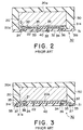
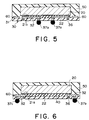
- Fig. 4 is a plan view of a film carrier semiconductor device according to an embodiment of the present invention.
- Fig. 5 is a cross-sectional view taken on line A-A' of Fig. 4 while Fig. 6 is a cross-sectional view taken on line B-B' of Fig. 4.
- a noise blocking layer is a difference between a film carrier semiconductor device 10 and the film carrier semiconductor device 10'.
- the film carrier semiconductor device 10 according to an embodiment of the present invention comprises the noise blocking layer 60 provided on the carrier film 30 along the periphery thereof on the side of the first surface 31a.
- the noise blocking layer 60 is outside the bare chip mounting region to form a closed loop.
- the chip electrodes 21 are located inside the closed loop of the noise blocking layer 60.
- the noise blocking layer 60 is electrically connected to at least one chip electrode 21a. In this embodiment, twenty chip electrodes 21a are connected to the noise blocking layer 60. The remaining chip electrodes, which are depicted by 21b, are connected to the bump electrodes 37. It is noted that there is no limitation on the number of the chip electrodes 21 and 21b.
- the noise blocking layer 60 is either a power supply layer or a ground layer. More specifically, the noise blocking layer 60 serves as the power supply layer when it is electrically connected to the chip electrode(s) 21a used as the electrode(s) for the power supply. Likewise, the noise blocking layer 60 acts as the ground layer when it is connected to the chip electrode(s) 21a used as the electrode(s) for the ground.
- the bump electrodes 37 located within the noise blocking loop are all for transmitting signals (bump electrodes 37a).
- the bump electrode 37b which is located outside the chip mounting region and is connected to the chip electrode 21b is used for the transmission of signals. In this event, the bump electrode 37b is not in contact with the noise blocking layer 60 as clearly shown in Fig. 6. It should be noted that the bump electrode 37b is not necessarily formed outside the chip mounting region. These bump electrodes 37b may be provided within the chip mounting region if this region has enough area for the bump electrodes 37a and 37b.
- the remaining bump electrodes 37c are either for grounding or for the power supply.
- the bump electrodes 37c are used for grounding when the noise blocking layer 60 is the ground layer.
- the bump electrodes 37c serve as the electrodes for the power supply when the noise blocking layer 60 is the power supply layer.
- the noise blocking layer 60 is made of a conductive material and is formed to have as large a width as possible in order to reduce the inductance thereof. In this event, the "width" of the noise blocking layer 60 means the distance in the direction depicted by W in Fig. 4.
- the demand for a larger number of bump electrodes 37 makes it necessary to use a longer interconnection layer 32. It is thus required to reduce the width of the interconnection layer in order to reduce the size of the semiconductor device.
- Such film carrier semiconductor device as illustrated in Fig. 1 is more likely to be affected by signal noise.
- the noise blocking layer 60 serves to reduce or even eliminate noise on the interconnection layers 32 after being connected with the chip electrodes.
- the noise blocking layer may be formed of two layers, i.e., the ground layer and the power supply layer rather than being formed as a single layer. In such a case, an insulation film or layer is interposed between the power supply layer and the ground layer.
Abstract

Description
- The present invention relates to a film carrier semiconductor device and, more particularly, to a film carrier semiconductor device which can advantageously be mounted on, for example, a circuit board at a high density.
- Semiconductor packages of various forms have been developed to meet recent demands in the electronics field towards size and weight reduction, speed increase, and improvement of functional operations of the packages. The semiconductor device comprises a package and a semiconductor chip (hereinafter, also referred to as a chip) contained in the package.
- The chip has become more and more highly integrated, and such a highly integrated semiconductor chip has an increased number of pins thereon. In addition, there have been severe demands on the semiconductor chips towards the possible reduction in size. The pin-to-pin lead pitch should thus be reduced to meet these demands or requirements for such semiconductor devices. A semiconductor device having a high pin count can be obtained by inner lead bonding or by area array bonding. The inner lead bonding and the area array bonding are expected to be inevitable for the field of the semiconductors.
- The inner lead bonding (ILB) is used to make electrical contact between the chip and the leads within the package. Various bonding technologies are available to achieve this inner lead bonding. Wire bonding is the most extensively used electrical interconnection process. In this process, fine wires are used to make electrical contact between the bonding pads on the chip and the corresponding leads on the package. The wire diameter is typically from 20 to 30 micrometers. Wire bonding techniques include thermocompression bonding, ultrasonic bonding, and thermosonic bonding.
- The use of the fine wires limits the number of interconnections available in one package. The recent demands for the semiconductor devices with a high pin count thus causes a problem of poor connections between the wire and the bonding pads. Considering this fact, the wire bonding has been replaced with wireless bonding. The wireless bonding is also called gang bonding, with which all bumps on the electrode pads (hereinafter, also referred to as pads) are bonded simultaneously to the leads. Wireless bonding techniques include tape automated bonding (TAB) and flip-chip bonding. The TAB bonding is also referred to as tape carrier bonding.
- In the TAB technique, a laminated tape of goldplated copper foil etched in the form of leads is bonded to the bumps on the chip pads. The elimination of the wire bonding is advantageous from viewpoints of size reduction and highly integrated packaging of the device. On the other hand, the flip-chip bonding requires to make a raised metallic bump of solder on the chip. The chip is then inverted and bonded face down to the substrate interconnection pattern. This process lends itself to production of semiconductor devices with a high pin count and a smaller pitch. In addition, this technique is also advantageous to provide a fast, low-noise semiconductor device with the short length of the interconnections.
- The TAB and flip-chip bonding techniques use the bumps provided between the chip and the film (package) to make electrical interconnection between them. These techniques are disclosed in, for example, Japanese Patent Laid-open Nos. 5-129366 and 6-77293.
- As mentioned above, the film carrier semiconductor device disclosed in these laid-open publications uses the bumps for the electrical interconnection between the chip and the carrier film. There is another film carrier semiconductor device in which the electrical interconnection between the chip and the carrier film is achieved without using the bumps. The semiconductor chip and the carrier film are electrically connected during the assembly process. The bumps are used only for the purpose of connecting the film carrier semiconductor device with, for example, a circuit board. The film carrier semiconductor device of the type described comprises a semiconductor chip and a carrier film. Contact pads are provided on the semiconductor chip at one side thereof. The contact pads are arranged along the periphery of the semiconductor chip. Interconnecting layers are provided on the carrier film. The carrier film is also provided with through-holes and openings formed therein. The openings are formed at the position corresponding to the contact pads.
- The bumps are formed on corresponding outer contact pads arranged as an array on the carrier film on the side facing to the substrate. The bumps are formed both within and outside the area corresponding to a chip mounting region. In this event, the bumps may be formed along the periphery of the chip and are connected to the chip electrodes through the interconnection layers. This structure causes a noise problem of the film carrier semiconductor device. More specifically, the bumps are arranged into an array and thus the bump located at or around the center of the array is connected to the corresponding chip electrode through a long interconnection layer. With a higher pin count, a longer interconnection layer may be required for the interconnection between the bump and the chip electrode. This raises the necessity to reduce the width of the wiring for a smaller semiconductor package. Such a long and thin wiring tends to be affected by noise from outside.
- Some approaches have been made to reduce the effect of noise on the semiconductor device. An example is disclosed in Japanese Patent Laid-open No. 2-186670, in which a semiconductor IC comprises a conductive region for power supply provided on a package on which a semiconductor chip is mounted. The conductive region surrounds the semiconductor chip and is connected with power supply pads on the semiconductor chip. The technique disclosed in this laid-open publication is provided only for the purpose of reducing the number of outer pins for the power supply. The power supply pads on the semiconductor chip are connected with the conductive region through bonding wires. In other words, the semiconductor IC disclosed there is associated with the wire bonding process, which is outside the scope of the field to which the present invention relates.
- Accordingly, an object of the preferred embodiments of the present invention is to provide a film carrier semiconductor device which is less affected by noise, has good electrical properties, and can meet a requirement, if any, for a higher pin count.
- In one aspect the invention provides a film carrier semiconductor device comprising a semiconductor chip having chip electrodes on one surface thereof; a carrier film adhered to said surface of the semiconductor chip, interconnections on the side of the carrier film facing said semiconductor chip being connected to the chip electrodes within a chip mounting region beneath said semiconductor chip; and characterised by a noise blocking means on said film outwardly of and extending around the chip mounting region.
- In another aspect of the prevent invention there is provided with a film carrier semiconductor device comprising a semiconductor bare chip having chip electrodes on one surface thereof; a resin for use in sealing the semiconductor bare chip; and a carrier film connected to the chip electrodes and adhered to the semiconductor bare chip on the side of the one surface, the carrier film being provided with interconnection layers on the side facing to the semiconductor bare chip within a chip mounting region corresponding to where the semiconductor bare chip is mounted, the film carrier semiconductor device further comprising a noise blocking layer provided along the periphery thereof outside the chip mounting region.
- Other aspects of the invention are as set out in the claims.
- The above and other bbjects, features and advantages of the present invention will become more apparent in the following description and the accompanying drawing in which like reference numerals refer to like parts and components.
-
- Fig. 1 is a plan view of a conventional film carrier semiconductor device;
- Fig. 2 is a cross-sectional view taken on line A-A' of Fig. 1;
- Fig. 3 is a cross-sectional view taken on line B-B' of Fig. 1;
- Fig. 4 is a plan view of a film carrier semiconductor device according to an embodiment of the present invention;
- Fig. 5 is a cross-sectional view taken on line A-A' of Fig. 4; and
- Fig. 6 is a cross-sectional view taken on line B-B' of Fig. 4.
- A conventional film carrier semiconductor device is described first for the purpose of facilitating the understanding of the present invention. Referring to Figs. 1 to 3, a film carrier semiconductor device 10' comprises a semiconductor
bare chip 20 and acarrier film 30. Anadhesion film 40 is interposed between thebare chip 20 and thecarrier film 30. Theadhesion film 40 is smaller than the semiconductorbare chip 20 and has a thickness of about several ten micrometers. The semiconductorbare chip 20 is prepared by using, for example, a well-known wafer manufacturing technique and has afirst surface 20a and asecond surface 20b. A plurality of contact pads (chip electrodes) 21 are provided on thebare chip 20 on the side of thesecond surface 20b. Thecontact pads 21 are arranged along the periphery of thebare chip 20 and each serves as an electrode for signals, for the power supply, or for the ground. Thecontact pads 21 may be, however, provided on thebare chip 20 within an active region. Thecontact pads 21 are typically made of an aluminum-based alloy. Thebare chip 20 is also provided with apassivation film 22 formed on thesecond surface 20b thereof. Thepassivation film 22 may be made of, for example, polyimide, silicon nitride, or silicon oxide. - The
carrier film 30 comprises anorganic insulation film 31. Theorganic insulation film 31 may be, for example, a polyimide-based insulation film. Theorganic insulation film 31 has a first surface 31a and a second surface 31b. Interconnection layers 32 are provided on theorganic insulation film 31 on the side of the first surface 31a. Through-holes 33 are formed in theinsulation film 31. One end of each through-hole 33 faces theinterconnection layer 32. Each through-hole 33 passes through theinsulation film 31 to the second surface 31b thereof. Theinsulation film 31 is also provided withopenings 34 penetrating through the film. Theopenings 34 are formed at the position corresponding to thecontact pads 21. Each through-hole 33 is filled with aconductive electrode 35. Likewise, each opening 34 is filled with afiller material 36. Theconductive electrode 35 contacts with one end of theinterconnection layer 32. The other end of theinterconnection layer 32 reaches between thecontact pad 21 and theopening 34. The entire structure of the chip and the package is sealed with aresin 50 to form a hermetic semiconductor device. - Solder bumps (bump electrodes) 37 are formed on corresponding outer contact pads arranged as an array on the
carrier film 30 at the second surface 31b thereof. The solder bumps 37 may be formed by using a method disclosed in, for example, Japanese Patent Laid-open No. 49-52973. The solder bumps 37 are formed by soldering a solder wire by using the wire bonding process on the surfaces of the semiconductor device corresponding to the pads on the chip. The balls are then bonded to the pads, following which the wires are cut. Some of the solder bumps 37 are formed within the area corresponding to a bare chip mounting region where thebare chip 20 is mounted. These solder bumps 37 are defined herein as a first group of the solder bumps. The remaining solder bumps 37 are formed outside the area corresponding to the bare chip mounting region. These bumps are defined herein as a second group of the solder bumps. If the bare chip mounting region is not enough for the bump electrodes, thebump electrodes 37 may be formed along the periphery of the chip as shown in Fig. 3. Considering the easy mounting of the semiconductor device on the circuit board or the like, thebump electrodes 37 may be arranged into an array at a pitch of 0.5 mm. As an example, the semiconductor chip mounting region has an area of 7 mm square available for forming the bump electrodes. Only two hundred and twenty-five pins, at maximum, can be formed within this region. To provide a region larger than the chip size for the bump formation, molding may advantageously be used. Fig. 1 shows the bump electrodes of which number is smaller by far than those formed in a practical process of manufacturing semiconductor devices. However, it can be understood by those skilled in the art that such few numbers of bump electrodes are merely for the purpose of simplifying the figure. It can also be understood that the number of the bumps and contact pads, as well as the pitch between them are not limited to the illustrated ones. - As mentioned above, the bump electrodes are arranged even along the periphery of the chip and are connected to the chip electrodes through the interconnection layer. This structure causes a noise problem of the film carrier semiconductor device 10'. The bump electrodes for mounting are arranged into an array. Accordingly, the bump electrode at or around the center of the array is connected to the corresponding chip electrode through a long interconnection layer. A longer interconnection layer may be required for the interconnection between the bump electrode and the chip electrode of the semiconductor device having a higher pin count. It is thus necessary to reduce the width of the wiring for a smaller semiconductor package. Such a long and thin wiring tends to be affected by noise from outside.
- An embodiment of the present invention is now described with reference to Figs. 4 to 6. Fig. 4 is a plan view of a film carrier semiconductor device according to an embodiment of the present invention. Fig. 5 is a cross-sectional view taken on line A-A' of Fig. 4 while Fig. 6 is a cross-sectional view taken on line B-B' of Fig. 4. A noise blocking layer is a difference between a film
carrier semiconductor device 10 and the film carrier semiconductor device 10'. More specifically, the filmcarrier semiconductor device 10 according to an embodiment of the present invention comprises thenoise blocking layer 60 provided on thecarrier film 30 along the periphery thereof on the side of the first surface 31a. Thenoise blocking layer 60 is outside the bare chip mounting region to form a closed loop. Thechip electrodes 21 are located inside the closed loop of thenoise blocking layer 60. Thenoise blocking layer 60 is electrically connected to at least onechip electrode 21a. In this embodiment, twentychip electrodes 21a are connected to thenoise blocking layer 60. The remaining chip electrodes, which are depicted by 21b, are connected to thebump electrodes 37. It is noted that there is no limitation on the number of thechip electrodes 21 and 21b. Thenoise blocking layer 60 is either a power supply layer or a ground layer. More specifically, thenoise blocking layer 60 serves as the power supply layer when it is electrically connected to the chip electrode(s) 21a used as the electrode(s) for the power supply. Likewise, thenoise blocking layer 60 acts as the ground layer when it is connected to the chip electrode(s) 21a used as the electrode(s) for the ground. - In this embodiment, the
bump electrodes 37 located within the noise blocking loop are all for transmitting signals (bumpelectrodes 37a). For thebump electrodes 37 located outside the chip mounting region, some are for transmitting signals and others not. Thebump electrode 37b which is located outside the chip mounting region and is connected to the chip electrode 21b is used for the transmission of signals. In this event, thebump electrode 37b is not in contact with thenoise blocking layer 60 as clearly shown in Fig. 6. It should be noted that thebump electrode 37b is not necessarily formed outside the chip mounting region. Thesebump electrodes 37b may be provided within the chip mounting region if this region has enough area for thebump electrodes bump electrodes 37c are either for grounding or for the power supply. More specifically, thebump electrodes 37c are used for grounding when thenoise blocking layer 60 is the ground layer. Likewise, thebump electrodes 37c serve as the electrodes for the power supply when thenoise blocking layer 60 is the power supply layer. Thenoise blocking layer 60 is made of a conductive material and is formed to have as large a width as possible in order to reduce the inductance thereof. In this event, the "width" of thenoise blocking layer 60 means the distance in the direction depicted by W in Fig. 4. - As mentioned above, the demand for a larger number of
bump electrodes 37 makes it necessary to use alonger interconnection layer 32. It is thus required to reduce the width of the interconnection layer in order to reduce the size of the semiconductor device. Such film carrier semiconductor device as illustrated in Fig. 1 is more likely to be affected by signal noise. On the contrary, thenoise blocking layer 60 serves to reduce or even eliminate noise on the interconnection layers 32 after being connected with the chip electrodes. - While having thus been described in conjunction with an illustrative embodiment, the present invention is not limited to this embodiment. Instead, it is apparent from those skilled in the art that various changes, modifications, and alternations may be made on the above mentioned embodiment without departing from the scope and spirit of the present invention. For example, the noise blocking layer may be formed of two layers, i.e., the ground layer and the power supply layer rather than being formed as a single layer. In such a case, an insulation film or layer is interposed between the power supply layer and the ground layer.
- Each feature disclosed in this specification (which term includes the claims) and/or shown in the drawings may be incorporated in the invention independently of other disclosed and/or illustrated features.
- The appended abstract as filed herewith is included in the specification by reference.
Claims (13)
- A film carrier semiconductor device (10) comprising a semiconductor chip (20) having chip electrodes (21) on one surface (20b) thereof; a carrier film (30) adhered to said surface of the semiconductor chip, interconnections (32) on the side of the carrier film facing said semiconductor chip being connected to the chip electrodes within a chip mounting region beneath said semiconductor chip; and characterised by a noise blocking means (60) on said film outwardly of and extending around the chip mounting region.
- A film carrier semiconductor device as claimed in claim 1, characterised in that said noise blocking means is a noise blocking layer.
- A film carrier semiconductor device (10) comprising a semiconductor bare chip (20) having chip electrodes (21) on one surface (20b) thereof; and a carrier film (30) connected to the chip electrodes and adhered to said semiconductor bare chip on the side of the one surface, said carrier film being provided with interconnection layers (32) on the side facing to said semiconductor bare chip with a chip mounting region corresponding to where said semiconductor bare chip is mounted, characterised in that said film carrier semiconductor device further comprises a noise blocking layer (60) provided along the periphery thereof outside the chip mounting region.
- A film carrier semiconductor device (10) comprising a semiconductor chip (20); a carrier film (30) having first and second surfaces (31a,31b), the first surface facing to said semiconductor chip; bump electrodes (37) provided on said carrier film on the side of the second surface, a first group of bump electrodes (37a) being located within a chip mounting region corresponding to where said semiconductor bare chip is mounted while a second group of said bump electrodes (37b,37c) being located outside the chip mounting region; chip electrodes (21) proved between said semiconductor chip and said carrier film, said chip electrodes each being located within the chip mounting region and electrically connected with said carrier film; interconnection layers (32) for connecting said chip electrodes and said bump electrodes of the first group, characterised in that said film carrier semiconductor device further comprises a noise blocking layer (60) provided on said carrier film outside the chip mounting region.
- A film carrier semiconductor device (10) comprising a semiconductor chip (20); a carrier film (30) having first and second surfaces (31a, 31b), the first surface facing to said semiconductor chip, said carrier film being larger in length and width than said semiconductor chip; bump electrodes (37) provided on said carrier film on the side of the second surface, a first group of bump electrodes (37a) being located within a chip mounting region corresponding to where said semiconductor bare chip is mounted while a second group of said bump electrodes (37b, 37c) being located outside the chip mounting region; chip electrodes (21) provided between said semiconductor chip and said carrier film, said chip electrodes each being located within the chip mounting region and electrically connected with said carrier film; interconnection layers (32) for connecting said chip electrodes and said bump electrodes of the first group, characterised in that said film carrier semiconductor device further comprises a noise blocking layer. (60) provided on said carrier film outside the chip mounting region.
- A film carrier semiconductor device as claimed in any of claims 2 to 5, characterised in that said noise blocking layer is made of a conductive material.
- A film carrier semiconductor device as claimed in any of claims 2 to 6, characterised in that said noise blocking layer is electrically connected to at least one of said chip electrodes.
- A film carrier semiconductor device as claimed in claim 6, characterised in that at least one of said chip electrodes is for supplying power to said device and said noise blocking layer serves as a power supply layer.
- A film carrier semiconductor device as claimed in claim 6, characterised in that at least one of said chip electrodes is for grounding said device and said noise blocking layer serves as a ground layer.
- A film carrier semiconductor device as claimed in claim 6, characterised in that said noise blocking layer is formed of two layers between which an insulation film (31) is interposed.
- A film carrier semiconductor device as claimed in claim 10, characterised in that one of the two layers is a power supply layer and the other is a ground layer, the power supply layer being electrically connected to said chip electrodes that are for use in supplying power to said device while the ground layer being electrically connected to said chip electrodes that are for grounding said device.
- A film carrier semiconductor device as claimed in any preceding claim, characterised in that said device is sealed to form a hermetic semiconductor device.
- A film carrier semiconductor device as claimed in claim 12, characterised in that said device is sealed with a resin.
Applications Claiming Priority (2)
| Application Number | Priority Date | Filing Date | Title |
|---|---|---|---|
| JP6237854A JP2546192B2 (en) | 1994-09-30 | 1994-09-30 | Film carrier semiconductor device |
| JP237854/94 | 1994-09-30 |
Publications (2)
| Publication Number | Publication Date |
|---|---|
| EP0704900A2 true EP0704900A2 (en) | 1996-04-03 |
| EP0704900A3 EP0704900A3 (en) | 1996-10-30 |
Family
ID=17021403
Family Applications (1)
| Application Number | Title | Priority Date | Filing Date |
|---|---|---|---|
| EP95306872A Withdrawn EP0704900A3 (en) | 1994-09-30 | 1995-09-28 | Film carrier semiconductor device |
Country Status (4)
| Country | Link |
|---|---|
| US (1) | US5726489A (en) |
| EP (1) | EP0704900A3 (en) |
| JP (1) | JP2546192B2 (en) |
| KR (1) | KR100209993B1 (en) |
Cited By (3)
| Publication number | Priority date | Publication date | Assignee | Title |
|---|---|---|---|---|
| WO1998040912A1 (en) * | 1997-03-10 | 1998-09-17 | Fraunhofer-Gesellschaft zur Förderung der angewandten Forschung e.V. | Chip arrangement and method for the production of the same |
| EP0950260A1 (en) * | 1996-04-02 | 1999-10-20 | Micron Technology, Inc. | Standardized bonding location process and apparatus |
| US6897096B2 (en) | 2002-08-15 | 2005-05-24 | Micron Technology, Inc. | Method of packaging semiconductor dice employing at least one redistribution layer |
Families Citing this family (50)
| Publication number | Priority date | Publication date | Assignee | Title |
|---|---|---|---|---|
| US5821608A (en) * | 1995-09-08 | 1998-10-13 | Tessera, Inc. | Laterally situated stress/strain relieving lead for a semiconductor chip package |
| KR0179802B1 (en) * | 1995-12-29 | 1999-03-20 | 문정환 | Semiconductor package |
| SG60099A1 (en) * | 1996-08-16 | 1999-02-22 | Sony Corp | Semiconductor package and manufacturing method of lead frame |
| US5866949A (en) * | 1996-12-02 | 1999-02-02 | Minnesota Mining And Manufacturing Company | Chip scale ball grid array for integrated circuit packaging |
| JP3695893B2 (en) * | 1996-12-03 | 2005-09-14 | 沖電気工業株式会社 | Semiconductor device, manufacturing method and mounting method thereof |
| JPH10335567A (en) * | 1997-05-30 | 1998-12-18 | Mitsubishi Electric Corp | Semiconductor integrated-circuit device |
| EP0993039B1 (en) * | 1997-06-26 | 2006-08-30 | Hitachi Chemical Company, Ltd. | Substrate for mounting semiconductor chips |
| JP3134815B2 (en) * | 1997-06-27 | 2001-02-13 | 日本電気株式会社 | Semiconductor device |
| JP3053010B2 (en) * | 1997-11-21 | 2000-06-19 | 日本電気株式会社 | Semiconductor device |
| JP3610787B2 (en) * | 1998-03-24 | 2005-01-19 | セイコーエプソン株式会社 | Semiconductor chip mounting structure, liquid crystal device and electronic apparatus |
| JPH11345905A (en) | 1998-06-02 | 1999-12-14 | Mitsubishi Electric Corp | Semiconductor device |
| US6133634A (en) * | 1998-08-05 | 2000-10-17 | Fairchild Semiconductor Corporation | High performance flip chip package |
| JP2000208540A (en) * | 1998-08-25 | 2000-07-28 | Texas Instr Inc <Ti> | Method for airtightly sealing thin semiconductor chip scale package |
| JP3339473B2 (en) * | 1999-08-26 | 2002-10-28 | 日本電気株式会社 | Package substrate, semiconductor device including the package substrate, and methods of manufacturing the same |
| US6544816B1 (en) * | 1999-08-20 | 2003-04-08 | Texas Instruments Incorporated | Method of encapsulating thin semiconductor chip-scale packages |
| KR100311090B1 (en) * | 1999-09-09 | 2001-10-12 | 김영우 | Fermenting agent and Fermenting method for organic wastes |
| JP2001156212A (en) * | 1999-09-16 | 2001-06-08 | Nec Corp | Resin sealed semiconductor device and producing method therefor |
| US6624522B2 (en) * | 2000-04-04 | 2003-09-23 | International Rectifier Corporation | Chip scale surface mounted device and process of manufacture |
| JP2003533048A (en) * | 2000-05-11 | 2003-11-05 | コーニンクレッカ フィリップス エレクトロニクス エヌ ヴィ | Semiconductor device and method of manufacturing semiconductor device |
| KR100418016B1 (en) * | 2000-07-31 | 2004-02-11 | (주)엠에스토피아 | Microorganism composition using as probiotics for growth promoting nutrient |
| KR100425591B1 (en) * | 2000-08-17 | 2004-04-03 | 최형석 | Medical compound for feed of cattle capable of reducing cholesterol and gaining weight |
| EP1233522A1 (en) * | 2001-02-14 | 2002-08-21 | Siemens Aktiengesellschaft | A data compression/decompression method and apparatus |
| US6930397B2 (en) * | 2001-03-28 | 2005-08-16 | International Rectifier Corporation | Surface mounted package with die bottom spaced from support board |
| US7119447B2 (en) * | 2001-03-28 | 2006-10-10 | International Rectifier Corporation | Direct fet device for high frequency application |
| US7476964B2 (en) * | 2001-06-18 | 2009-01-13 | International Rectifier Corporation | High voltage semiconductor device housing with increased clearance between housing can and die for improved flux flushing |
| US6582990B2 (en) | 2001-08-24 | 2003-06-24 | International Rectifier Corporation | Wafer level underfill and interconnect process |
| KR20030023412A (en) * | 2001-09-13 | 2003-03-19 | 윤선기 | The method of ferment for microbial on the a Chinese medicine. |
| US6784540B2 (en) | 2001-10-10 | 2004-08-31 | International Rectifier Corp. | Semiconductor device package with improved cooling |
| US6674174B2 (en) * | 2001-11-13 | 2004-01-06 | Skyworks Solutions, Inc. | Controlled impedance transmission lines in a redistribution layer |
| US7397137B2 (en) * | 2002-07-15 | 2008-07-08 | International Rectifier Corporation | Direct FET device for high frequency application |
| US7579697B2 (en) * | 2002-07-15 | 2009-08-25 | International Rectifier Corporation | Arrangement for high frequency application |
| JP3611561B2 (en) * | 2002-11-18 | 2005-01-19 | 沖電気工業株式会社 | Semiconductor device |
| US6841865B2 (en) * | 2002-11-22 | 2005-01-11 | International Rectifier Corporation | Semiconductor device having clips for connecting to external elements |
| JP3808030B2 (en) * | 2002-11-28 | 2006-08-09 | 沖電気工業株式会社 | Semiconductor device and manufacturing method thereof |
| US7038327B2 (en) * | 2003-11-11 | 2006-05-02 | Au Optronics Corp. | Anisotropic conductive film bonding pad |
| JP4010298B2 (en) * | 2003-12-17 | 2007-11-21 | セイコーエプソン株式会社 | Semiconductor device and manufacturing method thereof, circuit board, and electronic apparatus |
| TWI243386B (en) * | 2004-02-26 | 2005-11-11 | Au Optronics Corp | Anisotropic conductive film pad |
| US20050269677A1 (en) * | 2004-05-28 | 2005-12-08 | Martin Standing | Preparation of front contact for surface mounting |
| US7419852B2 (en) * | 2004-08-27 | 2008-09-02 | Micron Technology, Inc. | Low temperature methods of forming back side redistribution layers in association with through wafer interconnects, semiconductor devices including same, and assemblies |
| US11842972B2 (en) | 2004-09-28 | 2023-12-12 | Rohm Co., Ltd. | Semiconductor device with a semiconductor chip connected in a flip chip manner |
| JP2006100385A (en) | 2004-09-28 | 2006-04-13 | Rohm Co Ltd | Semiconductor device |
| US7524701B2 (en) * | 2005-04-20 | 2009-04-28 | International Rectifier Corporation | Chip-scale package |
| US7230333B2 (en) | 2005-04-21 | 2007-06-12 | International Rectifier Corporation | Semiconductor package |
| TWI365516B (en) * | 2005-04-22 | 2012-06-01 | Int Rectifier Corp | Chip-scale package |
| US20070224729A1 (en) * | 2006-03-21 | 2007-09-27 | Martin Reiss | Method for manufacturing a flip-chip package, substrate for manufacturing and flip-chip assembly |
| JP4795883B2 (en) * | 2006-07-21 | 2011-10-19 | 株式会社日立ハイテクノロジーズ | Pattern inspection / measurement equipment |
| JP5004654B2 (en) * | 2007-05-16 | 2012-08-22 | パナソニック株式会社 | Wiring board connection method and wiring board structure |
| US7851928B2 (en) * | 2008-06-10 | 2010-12-14 | Texas Instruments Incorporated | Semiconductor device having substrate with differentially plated copper and selective solder |
| KR101104326B1 (en) * | 2011-03-03 | 2012-01-16 | 이창해 | Feed additive |
| KR102243669B1 (en) * | 2015-01-26 | 2021-04-23 | 삼성전자주식회사 | Chip-on-film package and display device including the same |
Citations (2)
| Publication number | Priority date | Publication date | Assignee | Title |
|---|---|---|---|---|
| JPH05129366A (en) | 1991-11-08 | 1993-05-25 | Fujitsu Ltd | Tab mounting structure for integrated circuit use |
| JPH0677293A (en) | 1992-06-25 | 1994-03-18 | Nitto Denko Corp | Film carrier and semiconductor device using the same |
Family Cites Families (10)
| Publication number | Priority date | Publication date | Assignee | Title |
|---|---|---|---|---|
| JPS4952973A (en) * | 1972-09-22 | 1974-05-23 | ||
| US4937707A (en) * | 1988-05-26 | 1990-06-26 | International Business Machines Corporation | Flexible carrier for an electronic device |
| US4933741A (en) * | 1988-11-14 | 1990-06-12 | Motorola, Inc. | Multifunction ground plane |
| JPH02186670A (en) * | 1989-01-13 | 1990-07-20 | Nec Eng Ltd | Semiconductor integrated circuit |
| US4912547A (en) * | 1989-01-30 | 1990-03-27 | International Business Machines Corporation | Tape bonded semiconductor device |
| JP3061954B2 (en) * | 1991-08-20 | 2000-07-10 | 株式会社東芝 | Semiconductor device |
| JP2982450B2 (en) * | 1991-11-26 | 1999-11-22 | 日本電気株式会社 | Film carrier semiconductor device and method of manufacturing the same |
| JPH0828396B2 (en) * | 1992-01-31 | 1996-03-21 | 株式会社東芝 | Semiconductor device |
| US5214845A (en) * | 1992-05-11 | 1993-06-01 | Micron Technology, Inc. | Method for producing high speed integrated circuits |
| KR100280762B1 (en) * | 1992-11-03 | 2001-03-02 | 비센트 비.인그라시아 | Thermally Reinforced Semiconductor Devices Having Exposed Backsides and Methods of Manufacturing the Same |
-
1994
- 1994-09-30 JP JP6237854A patent/JP2546192B2/en not_active Expired - Fee Related
-
1995
- 1995-09-20 US US08/531,271 patent/US5726489A/en not_active Expired - Fee Related
- 1995-09-28 EP EP95306872A patent/EP0704900A3/en not_active Withdrawn
- 1995-09-29 KR KR1019950033148A patent/KR100209993B1/en not_active IP Right Cessation
Patent Citations (2)
| Publication number | Priority date | Publication date | Assignee | Title |
|---|---|---|---|---|
| JPH05129366A (en) | 1991-11-08 | 1993-05-25 | Fujitsu Ltd | Tab mounting structure for integrated circuit use |
| JPH0677293A (en) | 1992-06-25 | 1994-03-18 | Nitto Denko Corp | Film carrier and semiconductor device using the same |
Cited By (6)
| Publication number | Priority date | Publication date | Assignee | Title |
|---|---|---|---|---|
| EP0950260A1 (en) * | 1996-04-02 | 1999-10-20 | Micron Technology, Inc. | Standardized bonding location process and apparatus |
| EP0950260A4 (en) * | 1996-04-02 | 1999-10-20 | ||
| US6048753A (en) * | 1996-04-02 | 2000-04-11 | Micron Technology, Inc. | Standardized bonding location process and apparatus |
| WO1998040912A1 (en) * | 1997-03-10 | 1998-09-17 | Fraunhofer-Gesellschaft zur Förderung der angewandten Forschung e.V. | Chip arrangement and method for the production of the same |
| US6897096B2 (en) | 2002-08-15 | 2005-05-24 | Micron Technology, Inc. | Method of packaging semiconductor dice employing at least one redistribution layer |
| US6965160B2 (en) | 2002-08-15 | 2005-11-15 | Micron Technology, Inc. | Semiconductor dice packages employing at least one redistribution layer |
Also Published As
| Publication number | Publication date |
|---|---|
| JPH08102473A (en) | 1996-04-16 |
| KR960012396A (en) | 1996-04-20 |
| KR100209993B1 (en) | 1999-07-15 |
| EP0704900A3 (en) | 1996-10-30 |
| JP2546192B2 (en) | 1996-10-23 |
| US5726489A (en) | 1998-03-10 |
Similar Documents
| Publication | Publication Date | Title |
|---|---|---|
| US5726489A (en) | Film carrier semiconductor device | |
| KR100339044B1 (en) | ball grid array semiconductor package and method for making the same | |
| US7511376B2 (en) | Circuitry component with metal layer over die and extending to place not over die | |
| US9030029B2 (en) | Chip package with die and substrate | |
| US5468994A (en) | High pin count package for semiconductor device | |
| US6201302B1 (en) | Semiconductor package having multi-dies | |
| US7595222B2 (en) | Semiconductor device and manufacturing method thereof | |
| US5801448A (en) | Conductive lines on the back side of wafers and dice for semiconductor interconnects | |
| US6608376B1 (en) | Integrated circuit package substrate with high density routing mechanism | |
| US6812066B2 (en) | Semiconductor device having an interconnecting post formed on an interposer within a sealing resin | |
| US7898058B2 (en) | Integrated chip package structure using organic substrate and method of manufacturing the same | |
| US5289346A (en) | Peripheral to area adapter with protective bumper for an integrated circuit chip | |
| US5668409A (en) | Integrated circuit with edge connections and method | |
| US9240372B1 (en) | Semiconductor die having lead wires formed over a circuit in a shielded area | |
| JPH0595015A (en) | Semiconductor device | |
| US11784129B2 (en) | Semiconductor package and method of fabricating the same | |
| US20090146314A1 (en) | Semiconductor Device | |
| EP3547364B1 (en) | Semiconductor chip and semiconductor package including the same | |
| US5757068A (en) | Carrier film with peripheral slits | |
| US5426319A (en) | High-frequency semiconductor device including microstrip transmission line | |
| CN113224013A (en) | Semiconductor device package and method of manufacturing the same | |
| US11830798B2 (en) | Semiconductor device package | |
| US7605475B2 (en) | Semiconductor device | |
| US20190214367A1 (en) | Stacked package and a manufacturing method of the same | |
| US6624008B2 (en) | Semiconductor chip installing tape, semiconductor device and a method for fabricating thereof |
Legal Events
| Date | Code | Title | Description |
|---|---|---|---|
| PUAI | Public reference made under article 153(3) epc to a published international application that has entered the european phase |
Free format text: ORIGINAL CODE: 0009012 |
|
| AK | Designated contracting states |
Kind code of ref document: A2 Designated state(s): DE FR GB |
|
| PUAL | Search report despatched |
Free format text: ORIGINAL CODE: 0009013 |
|
| AK | Designated contracting states |
Kind code of ref document: A3 Designated state(s): DE FR GB |
|
| 17P | Request for examination filed |
Effective date: 19961004 |
|
| 17Q | First examination report despatched |
Effective date: 19990208 |
|
| RAP1 | Party data changed (applicant data changed or rights of an application transferred) |
Owner name: NEC ELECTRONICS CORPORATION |
|
| GRAH | Despatch of communication of intention to grant a patent |
Free format text: ORIGINAL CODE: EPIDOS IGRA |
|
| STAA | Information on the status of an ep patent application or granted ep patent |
Free format text: STATUS: THE APPLICATION HAS BEEN WITHDRAWN |
|
| 18W | Application withdrawn |
Effective date: 20030901 |