EP0704882A2 - Formation of closely spaced metal electrodes in a semiconductor device - Google Patents
Formation of closely spaced metal electrodes in a semiconductor device Download PDFInfo
- Publication number
- EP0704882A2 EP0704882A2 EP95111003A EP95111003A EP0704882A2 EP 0704882 A2 EP0704882 A2 EP 0704882A2 EP 95111003 A EP95111003 A EP 95111003A EP 95111003 A EP95111003 A EP 95111003A EP 0704882 A2 EP0704882 A2 EP 0704882A2
- Authority
- EP
- European Patent Office
- Prior art keywords
- layer
- electrode
- semiconductor layer
- semiconductor
- providing
- Prior art date
- Legal status (The legal status is an assumption and is not a legal conclusion. Google has not performed a legal analysis and makes no representation as to the accuracy of the status listed.)
- Granted
Links
- 239000004065 semiconductor Substances 0.000 title claims abstract description 173
- 239000002184 metal Substances 0.000 title claims abstract description 76
- 229910052751 metal Inorganic materials 0.000 title claims abstract description 76
- 230000015572 biosynthetic process Effects 0.000 title description 2
- 229920002120 photoresistant polymer Polymers 0.000 claims abstract description 74
- 238000000034 method Methods 0.000 claims abstract description 63
- 238000005530 etching Methods 0.000 claims description 9
- 239000003989 dielectric material Substances 0.000 claims description 3
- 238000001459 lithography Methods 0.000 claims description 3
- 238000000059 patterning Methods 0.000 claims 1
- 238000000151 deposition Methods 0.000 abstract description 3
- 230000008021 deposition Effects 0.000 abstract 1
- 238000001465 metallisation Methods 0.000 description 9
- 238000000926 separation method Methods 0.000 description 5
- VYPSYNLAJGMNEJ-UHFFFAOYSA-N Silicium dioxide Chemical compound O=[Si]=O VYPSYNLAJGMNEJ-UHFFFAOYSA-N 0.000 description 4
- 239000000463 material Substances 0.000 description 4
- 229910052581 Si3N4 Inorganic materials 0.000 description 2
- MVPPADPHJFYWMZ-UHFFFAOYSA-N chlorobenzene Chemical compound ClC1=CC=CC=C1 MVPPADPHJFYWMZ-UHFFFAOYSA-N 0.000 description 2
- 238000005516 engineering process Methods 0.000 description 2
- 150000002739 metals Chemical class 0.000 description 2
- 238000001020 plasma etching Methods 0.000 description 2
- 235000012239 silicon dioxide Nutrition 0.000 description 2
- 239000000377 silicon dioxide Substances 0.000 description 2
- HQVNEWCFYHHQES-UHFFFAOYSA-N silicon nitride Chemical compound N12[Si]34N5[Si]62N3[Si]51N64 HQVNEWCFYHHQES-UHFFFAOYSA-N 0.000 description 2
- 125000006850 spacer group Chemical group 0.000 description 2
- QVGXLLKOCUKJST-UHFFFAOYSA-N atomic oxygen Chemical compound [O] QVGXLLKOCUKJST-UHFFFAOYSA-N 0.000 description 1
- 239000011248 coating agent Substances 0.000 description 1
- 238000000576 coating method Methods 0.000 description 1
- 238000005137 deposition process Methods 0.000 description 1
- 238000001312 dry etching Methods 0.000 description 1
- 230000008020 evaporation Effects 0.000 description 1
- 238000001704 evaporation Methods 0.000 description 1
- -1 gold Chemical class 0.000 description 1
- PCHJSUWPFVWCPO-UHFFFAOYSA-N gold Chemical compound [Au] PCHJSUWPFVWCPO-UHFFFAOYSA-N 0.000 description 1
- 239000010931 gold Substances 0.000 description 1
- 229910052737 gold Inorganic materials 0.000 description 1
- 238000012986 modification Methods 0.000 description 1
- 230000004048 modification Effects 0.000 description 1
- 229910052760 oxygen Inorganic materials 0.000 description 1
- 239000001301 oxygen Substances 0.000 description 1
- 230000003071 parasitic effect Effects 0.000 description 1
- 238000001039 wet etching Methods 0.000 description 1
Images
Classifications
-
- H—ELECTRICITY
- H01—ELECTRIC ELEMENTS
- H01L—SEMICONDUCTOR DEVICES NOT COVERED BY CLASS H10
- H01L21/00—Processes or apparatus adapted for the manufacture or treatment of semiconductor or solid state devices or of parts thereof
- H01L21/02—Manufacture or treatment of semiconductor devices or of parts thereof
- H01L21/04—Manufacture or treatment of semiconductor devices or of parts thereof the devices having at least one potential-jump barrier or surface barrier, e.g. PN junction, depletion layer or carrier concentration layer
- H01L21/18—Manufacture or treatment of semiconductor devices or of parts thereof the devices having at least one potential-jump barrier or surface barrier, e.g. PN junction, depletion layer or carrier concentration layer the devices having semiconductor bodies comprising elements of Group IV of the Periodic System or AIIIBV compounds with or without impurities, e.g. doping materials
- H01L21/28—Manufacture of electrodes on semiconductor bodies using processes or apparatus not provided for in groups H01L21/20 - H01L21/268
-
- H—ELECTRICITY
- H01—ELECTRIC ELEMENTS
- H01L—SEMICONDUCTOR DEVICES NOT COVERED BY CLASS H10
- H01L29/00—Semiconductor devices adapted for rectifying, amplifying, oscillating or switching, or capacitors or resistors with at least one potential-jump barrier or surface barrier, e.g. PN junction depletion layer or carrier concentration layer; Details of semiconductor bodies or of electrodes thereof ; Multistep manufacturing processes therefor
- H01L29/66—Types of semiconductor device ; Multistep manufacturing processes therefor
- H01L29/66007—Multistep manufacturing processes
- H01L29/66075—Multistep manufacturing processes of devices having semiconductor bodies comprising group 14 or group 13/15 materials
- H01L29/66227—Multistep manufacturing processes of devices having semiconductor bodies comprising group 14 or group 13/15 materials the devices being controllable only by the electric current supplied or the electric potential applied, to an electrode which does not carry the current to be rectified, amplified or switched, e.g. three-terminal devices
- H01L29/66234—Bipolar junction transistors [BJT]
- H01L29/6631—Bipolar junction transistors [BJT] with an active layer made of a group 13/15 material
- H01L29/66318—Heterojunction transistors
Definitions
- This invention relates generally to a method for forming metal electrodes on a semiconductor device and, more particularly, to a method for forming closely spaced metal electrodes electrically connected to different layers of a semiconductor device that provides reliable and reproducible vertical and horizontal separation of the electrodes.
- CMOS complementary metal-oxide-semiconductor
- CMOS complementary metal-oxide-semiconductor
- CMOS complementary metal-oxide-semiconductor
- HBT heterojunction bipolar transistor
- the top layer of a semiconductor device is thin, or the metal contacting an adjacent semiconductor layer, such as the base of an HBT, needs to be of a comparable thickness to that of the emitter region, the spacing between the two metal layers forming the electrodes may be very small resulting in the formation of metal electrodes which are likely to cause short circuits.
- Increasing the thickness of the top semiconductor layer would provide better separation of the electrodes, but might increase the parasitic resistance of this layer, and thus will reduce the etch reproducibility for forming narrow (sub micron) top semiconductor layer widths.
- a process for forming closely spaced metal electrodes for adjacent semiconductor layers of a high performance semiconductor device is disclosed.
- a sacrificial layer is first deposited over the semiconductor device.
- a photoresist is then deposited over the sacrificial layer, and is exposed and developed to form a re-entrant profile opening through the photoresist.
- the sacrificial layer is anisotropically etched through the re-entrant profile opening to expose the first semiconductor layer so as to provide a region of the first semiconductor layer to be contacted with the metal electrode.
- the width of the metal electrode and the lateral spacing between a semiconductor region formed from the first semiconductor layer and a metal electrode in contact with a second semiconductor layer are controlled by enlarging the re-entrant profile opening by an isotropic or anisotropic etch of the photoresist.
- the thickness of the sacrificial layer controls the vertical separation between electrode extensions of the metal electrode in contact with the first semiconductor layer and the metal electrode in contact with the second semiconductor layer.
- a metalization layer is formed over the developing structure such that metal is deposited on the first semiconductor layer.
- the photoresist is dissolved to remove the portions of the metal layer which do not form part of the electrode.
- the sacrificial layer and first semiconductor layer are etched to remove the sacrificial layer and form the semiconductor region from the first semiconductor layer.
- a second photoresist is deposited over the structure and a re-entrant profile opening is formed in the second photoresist to define the area which will be metalized to form the electrode for the second semiconductor layer.
- Metal is deposited over the entire structure such that electrodes are formed in contact with the second semiconductor layer.
- the second photoresist is dissolved such that metal which was not part of either electrode is removed.
- the second electrode can be formed by a metal deposition over the entire device, and then using conventional lithography techniques to pattern and etch this electrode by wet or dry etching. This process can be extended to providing metal electrodes for three or more semiconductor layers by covering the first metal electrode with a second sacrificial layer prior to the coating of the second photoresist.
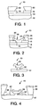
- Figures 1-5 are profile views of a developing semiconductor structure 10 that show sequential steps in a process for forming closely spaced metal electrodes in a high performance semiconductor device. Although the sequence of steps is novel in nature, each individual step can be performed by known processes in the art and therefore a detailed description of the process of each individual step would not be necessary to enable one of ordinary skill in the art to perform these steps.
- a lower semiconductor layer 12 and an upper semiconductor layer 14 are shown.
- the lower layer 12 could be a base layer and the upper layer 14 could be an emitter layer of an HBT, well known to those skilled in the art.
- the HBT would obviously include other layers which are not shown, such as a collector layer, and further, at least the emitter layer 14 would include a plurality of emitter layers.
- describing the layer 12 as a base layer and the layer 14 as an emitter layer is just by way of example as the process described below would be applicable to forming closely spaced electrodes for other semiconductor devices. The discussion below will describe a process of forming closely spaced metal contact electrodes to each of the upper and lower semiconductor layers 14 and 12.
- a thin sacrificial layer 16 is deposited over the semiconductor layer 14 by a suitable deposition process.
- the sacrificial layer 16 would typically be a dielectric material, such as silicon nitride (Si3N4) or silicon dioxide (SiO2); however, any appropriate material that has the property of being able to be etched isotopically and anisotropically with good selectivity to semiconductor material and metal electrodes could also be used.
- the thickness of the sacrificial layer 16 determines the vertical distance of an electrode contacting the semiconductor layer 14 from an electrode contacting the semiconductor layer 12, as will become apparent from the discussion below.
- the sacrificial layer 16 is shown in Figure 1 as having an opening 18 which exposes the semiconductor layer 14.
- a photoresist layer 20 is deposited over the sacrificial layer 16.
- the photoresist layer 20 can be any applicable photoresist that can be patterned to have a re-entrant or negative profile, such as a chlorobenzene treated liftoff resist or a negative i-line resist, known to those skilled in the art.
- the photoresist layer 20 is patterned and developed to form an opening 22 in the photoresist layer 20 having a re-entrant profile in a manner well understood to those skilled in the art.
- the size of the re-entrant profile opening 22 is approximately equal to the desired metal contact area of the upper semiconductor layer 14 as set by the opening 18.
- the re-entrant profile opening 22 is a product of the developing step of the photoresist layer 20. Other re-entrant profiles formed by other resists and developing procedures may also be used.
- the sacrificial layer 16 is anisotropically etched through the opening 22, by a procedure such as RIE (reactive ion etching), to expose the upper semiconductor layer 14 in order to generate the profile as shown in Figure 1.
- Figure 2 shows that the opening 22 in the photoresist layer 20 has been enlarged.
- This enlarging step can be performed by an oxygen plasma, or other form of dissolving a portion of the photoresist layer 20, to achieve a controlled size increase in the opening 22.
- the increase in the size of the opening 22 determines the width of electrode wings extending over the sacrificial layer 16, and will later determine the lateral spacing between a semiconductor etched region of the layer 14 and a lower semiconductor layer metal electrode.
- a metal layer 26 is deposited by an appropriate metalization process, such as evaporation, over the entire developing structure 10 so as to cause a metal electrode 28 to be deposited in contact with the semiconductor layer 14.
- the electrode 28 includes winged portions 30 which are formed on the top surface of the sacrificial layer 16. The distance between the edge of the opening 18 and the edge of the opening 22 defines the size of the winged portions 30.
- Figure 3 shows the electrode 28 being positioned in contact with a semiconductor region 32 which was part of the upper semiconductor layer 14.
- the photoresist layer 20 is dissolved so as to remove the excess portion of the metal layer 26 that was not part of the electrode 28.
- an isotropic or a combined isotropic/anisotropic etch is performed to remove both the sacrificial layer 16 and the portion of the semiconductor layer 14 which is not part of the semiconductor region 32.
- an isotropic etch will provide lateral removal of material such that the material beneath the electrode 28 can be removed to form the desired dimension of the semiconductor region 32. Etches of this type are well known in the art and the process of defining the semiconductor region 32 would be well understood.
- the electrode 28 is used as a mask to define the region 32 for the isotropic or combined isotropic and anisotropic etch of the semiconductor layer 14.
- a second photoresist layer 36 is deposited over the structure 10.
- a re-entrant profile opening 38 is formed in the photoresist layer 36 to expose the region of the semiconductor layer 12 which will be metalized.
- the method of forming the re-entrant profile opening 38 is the same as any of the methods of forming the re-entrant profile opening 22 discussed above.
- the re-entrant profile opening 38 can completely surround the electrode 28 as shown, or can partially cover the electrode 28.
- a metal layer 40 is evaporated over the structure 10 such that a portion of the metal layer 40 forms an electrode 42 in contact with the semiconductor layer 12, and a portion of the metal layer 40 is combined with the electrode 28.
- the electrode 42 appears to be two electrodes. However, for an HBT base electrode, the electrode 42 would be a single electrode surrounding the emitter region 32. That is not to say that this process isn't applicable to forming more than one electrode by a single metalization step.
- Figure 5 shows that the photoresist layer 36 has been dissolved to remove the portions of the metal layer 40 which do not form the electrode 42 or the electrode 28.
- the edges of the electrode 42 vertically align with the edges of the electrode 28.
- the amount that the opening 22 in the photoresist layer 20 is enlarged determines the lateral spacing between the semiconductor region 32 and the electrode 42.
- the thickness of the layer 16 which forms the vertical winged portions 30 of the electrode 28 determines the vertical separation of the electrode 28 and the electrode 42. In this manner, the vertical spacing of the electrodes 28 and 42 and the lateral spacing between semiconductor layer 32 and the electrode 42 can be controlled independently of the thickness of the semiconductor layer 14 or the thickness of the electrode 42.
- the process of forming the electrode 42 described above is one way of forming this electrode.
- the electrode 42 can be formed by depositing a metal layer over the entire structure 10 shown in Figure 3. Then, by using conventional lithography techniques, this metal layer can be patterned and etched by an appropriate wet or dry etch to form the electrode 42 in a manner that is well understood in the art. In this process, a single metalization step can be used to form multiple electrodes.
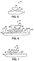
- Figures 6 and 7 are profile views of a developing semiconductor structure 50 showing how the above-described process can be extended to forming metal electrodes for three semiconductor layers.
- the semiconductor structure 50 could also be a heterojunction bipolar transistor.
- a semiconductor layer 52 could be a collector layer
- a semiconductor layer 54 could be a base layer
- a semiconductor layer 56 could be an emitter layer of an HBT.
- an electrode 58 could be an electrode connected to the collector layer 52
- an electrode 60 could be an electrode connected to the base layer 54
- an electrode 62 could be an electrode connected to the emitter layer 56.
- the electrode 62 would be the same as the electrode 28, and the electrode 60 would be the same as the electrode 42.
- a sacrificial layer (not shown), similar to the sacrificial layer 16 discussed above, would be deposited over the structure 50 after the metal lift-off procedure which removed the metal layer that formed the first electrode 62 and the etch which produced the semiconductor emitter layer 56.
- a sacrificial layer would be deposited over this structure, and a photoresist layer would be deposited over the sacrificial layer.
- the photoresist layer would be patterned to form a re-entrant profile opening which defined the dimensions of the electrode 60 just as the sacrificial layer 16 and photoresist layer 20 defined the dimensions of the electrode 28 discussed above.
- the electrode 60 also has winged portions similar to the wing portions 30 of the electrode 28.
- a third photoresist layer 64 is deposited over the structure 50.
- Re-entrant profile openings 66 are formed in the photoresist layer 64 to expose the region of the semiconductor collector layer 52 which is to be metalized to produce the electrodes 58.
- a metal layer 68 is evaporated over the structure 50 such that a portion of the metal layer 68 forms the electrodes 58 in contact with the semiconductor region 52.
- Figure 7 shows that the photoresist layer 66 has been dissolved to remove the portions of the metal layer 68 which do not form the electrodes 58.
- the edges of the electrode 58 vertically align with the edges of the electrode 60.
- the electrode 62 and a portion of the electrode 60 would be covered by the third photoresist layer so that the third electrode metal deposition does not reduce the vertical clearance between the electrodes 60 and 62.
Abstract


Description
- This invention relates generally to a method for forming metal electrodes on a semiconductor device and, more particularly, to a method for forming closely spaced metal electrodes electrically connected to different layers of a semiconductor device that provides reliable and reproducible vertical and horizontal separation of the electrodes.
- Semiconductor device performance has been continually improving. In order for semiconductor devices to operate at increasing speeds, the size of the devices has been becoming smaller. As the devices become smaller, the spacing between electrodes connected to different regions of the device needs to be closer together. Additionally, in order to realize higher device performance, the contact resistance between an electrode and the region of the device the electrode contacts must be minimized. An electrode metalization process which would provide contact to the entire surface area of a semiconductor region would result in a minimum contact resistance to that region.
- Although it is relatively straightforward to provide complete metal electrode coverage to a single semiconductor region, it is much more difficult to metalize adjacent semiconductor regions with complete or nearly complete metal coverage. Clearly, some minimum space between metal electrodes contacting different semiconductor regions is required to prevent electrical shorts. It is therefore difficult to achieve minimum spacing between two metal electrodes with a reliable, reproducible process. Consequently, device performance is limited by the ability of metalization processes in achieving minimum electrode spacing.
- Known processes of forming closely spaced metal electrodes in high performance semiconductor devices typically include using a recess of an etched top layer of the semiconductor device to provide the spacing between adjacent contact metal layers forming electrodes for two semiconductor regions. For example, the emitter metal of a heterojunction bipolar transistor (HBT) could be used as a mask to etch the emitter region of the HBT, thus forming a recess for a self-aligned base metalization. If the top layer of a semiconductor device is thin, or the metal contacting an adjacent semiconductor layer, such as the base of an HBT, needs to be of a comparable thickness to that of the emitter region, the spacing between the two metal layers forming the electrodes may be very small resulting in the formation of metal electrodes which are likely to cause short circuits. Increasing the thickness of the top semiconductor layer would provide better separation of the electrodes, but might increase the parasitic resistance of this layer, and thus will reduce the etch reproducibility for forming narrow (sub micron) top semiconductor layer widths.
- Further, other known processes of forming closely spaced metal electrodes in high performance semiconductor devices that use dielectric spacer technology are not readily effective with certain contact metals, such as gold, that are difficult to etch by the techniques that are compatible with dielectric spacer technology.
- What is needed is a reliable and reproducible process for forming metal electrodes in a high performance semiconductor device which produces minimum separation between an electrode of one semiconductor layer and an electrode for adjacent semiconductor layers that is independent of the semiconductor layer thicknesses or of the metals being used to contact the semiconductor layers. It is therefore an object of the present invention to provide such a process.
- In accordance with the teachings of the present invention, a process for forming closely spaced metal electrodes for adjacent semiconductor layers of a high performance semiconductor device is disclosed. In order to form a metal electrode for a first semiconductor layer of the semiconductor device, a sacrificial layer is first deposited over the semiconductor device. A photoresist is then deposited over the sacrificial layer, and is exposed and developed to form a re-entrant profile opening through the photoresist. The sacrificial layer is anisotropically etched through the re-entrant profile opening to expose the first semiconductor layer so as to provide a region of the first semiconductor layer to be contacted with the metal electrode. The width of the metal electrode and the lateral spacing between a semiconductor region formed from the first semiconductor layer and a metal electrode in contact with a second semiconductor layer are controlled by enlarging the re-entrant profile opening by an isotropic or anisotropic etch of the photoresist. The thickness of the sacrificial layer controls the vertical separation between electrode extensions of the metal electrode in contact with the first semiconductor layer and the metal electrode in contact with the second semiconductor layer. A metalization layer is formed over the developing structure such that metal is deposited on the first semiconductor layer. The photoresist is dissolved to remove the portions of the metal layer which do not form part of the electrode. Next, the sacrificial layer and first semiconductor layer are etched to remove the sacrificial layer and form the semiconductor region from the first semiconductor layer.
- To form the metal electrode for the second semiconductor layer of the semiconductor device, a second photoresist is deposited over the structure and a re-entrant profile opening is formed in the second photoresist to define the area which will be metalized to form the electrode for the second semiconductor layer. Metal is deposited over the entire structure such that electrodes are formed in contact with the second semiconductor layer. The second photoresist is dissolved such that metal which was not part of either electrode is removed. Alternatively, the second electrode can be formed by a metal deposition over the entire device, and then using conventional lithography techniques to pattern and etch this electrode by wet or dry etching. This process can be extended to providing metal electrodes for three or more semiconductor layers by covering the first metal electrode with a second sacrificial layer prior to the coating of the second photoresist.
- Additional objects, advantages, and features of the present invention will become apparent from the following description and appended claims, taken in conjunction with the accompanying drawings.
-
- Figures 1-5 are profile views of a developing semiconductor structure that show a sequential process of forming adjacent metal electrodes connected to adjacent semiconductor layers in a high performance semiconductor device according to a preferred embodiment of the present invention; and
- Figures 6 and 7 are profile views of a developing semiconductor structure for extending the process of Figures 1-5 to three metal electrodes for three semiconductor layers.
- The following description of the preferred embodiments concerning fabricating of closely spaced metal electrodes in a high performance semiconductor device is merely exemplary in nature and is in no way intended to limit the invention or its application or uses.
- Figures 1-5 are profile views of a developing
semiconductor structure 10 that show sequential steps in a process for forming closely spaced metal electrodes in a high performance semiconductor device. Although the sequence of steps is novel in nature, each individual step can be performed by known processes in the art and therefore a detailed description of the process of each individual step would not be necessary to enable one of ordinary skill in the art to perform these steps. - Starting with Figure 1, a
lower semiconductor layer 12 and anupper semiconductor layer 14 are shown. Thelower layer 12 could be a base layer and theupper layer 14 could be an emitter layer of an HBT, well known to those skilled in the art. The HBT would obviously include other layers which are not shown, such as a collector layer, and further, at least theemitter layer 14 would include a plurality of emitter layers. It will be appreciated that describing thelayer 12 as a base layer and thelayer 14 as an emitter layer is just by way of example as the process described below would be applicable to forming closely spaced electrodes for other semiconductor devices. The discussion below will describe a process of forming closely spaced metal contact electrodes to each of the upper andlower semiconductor layers - A thin
sacrificial layer 16 is deposited over thesemiconductor layer 14 by a suitable deposition process. Thesacrificial layer 16 would typically be a dielectric material, such as silicon nitride (Si₃N₄) or silicon dioxide (SiO₂); however, any appropriate material that has the property of being able to be etched isotopically and anisotropically with good selectivity to semiconductor material and metal electrodes could also be used. The thickness of thesacrificial layer 16 determines the vertical distance of an electrode contacting thesemiconductor layer 14 from an electrode contacting thesemiconductor layer 12, as will become apparent from the discussion below. - The
sacrificial layer 16 is shown in Figure 1 as having anopening 18 which exposes thesemiconductor layer 14. However, prior to forming theopening 18, aphotoresist layer 20 is deposited over thesacrificial layer 16. Thephotoresist layer 20 can be any applicable photoresist that can be patterned to have a re-entrant or negative profile, such as a chlorobenzene treated liftoff resist or a negative i-line resist, known to those skilled in the art. Once thephotoresist layer 20 is deposited over thesacrificial layer 16, thephotoresist layer 20 is patterned and developed to form anopening 22 in thephotoresist layer 20 having a re-entrant profile in a manner well understood to those skilled in the art. The size of there-entrant profile opening 22 is approximately equal to the desired metal contact area of theupper semiconductor layer 14 as set by theopening 18. The re-entrant profile opening 22 is a product of the developing step of thephotoresist layer 20. Other re-entrant profiles formed by other resists and developing procedures may also be used. Once there-entrant profile opening 22 is formed in thephotoresist layer 20, thesacrificial layer 16 is anisotropically etched through theopening 22, by a procedure such as RIE (reactive ion etching), to expose theupper semiconductor layer 14 in order to generate the profile as shown in Figure 1. - Now turning to Figure 2, the next steps of the process will be discussed. Figure 2 shows that the
opening 22 in thephotoresist layer 20 has been enlarged. This enlarging step can be performed by an oxygen plasma, or other form of dissolving a portion of thephotoresist layer 20, to achieve a controlled size increase in theopening 22. The increase in the size of theopening 22 determines the width of electrode wings extending over thesacrificial layer 16, and will later determine the lateral spacing between a semiconductor etched region of thelayer 14 and a lower semiconductor layer metal electrode. Next, ametal layer 26 is deposited by an appropriate metalization process, such as evaporation, over the entire developingstructure 10 so as to cause ametal electrode 28 to be deposited in contact with thesemiconductor layer 14. As is apparent, theelectrode 28 includeswinged portions 30 which are formed on the top surface of thesacrificial layer 16. The distance between the edge of theopening 18 and the edge of theopening 22 defines the size of thewinged portions 30. - Figure 3 shows the
electrode 28 being positioned in contact with asemiconductor region 32 which was part of theupper semiconductor layer 14. To arrive at this profile, thephotoresist layer 20 is dissolved so as to remove the excess portion of themetal layer 26 that was not part of theelectrode 28. Next, an isotropic or a combined isotropic/anisotropic etch is performed to remove both thesacrificial layer 16 and the portion of thesemiconductor layer 14 which is not part of thesemiconductor region 32. As is well understood, an isotropic etch will provide lateral removal of material such that the material beneath theelectrode 28 can be removed to form the desired dimension of thesemiconductor region 32. Etches of this type are well known in the art and the process of defining thesemiconductor region 32 would be well understood. Theelectrode 28 is used as a mask to define theregion 32 for the isotropic or combined isotropic and anisotropic etch of thesemiconductor layer 14. - Now turning to Figure 4, the steps for generating the metal electrode in contact with the
lower semiconductor layer 12 will be discussed. Asecond photoresist layer 36 is deposited over thestructure 10. Are-entrant profile opening 38 is formed in thephotoresist layer 36 to expose the region of thesemiconductor layer 12 which will be metalized. The method of forming there-entrant profile opening 38 is the same as any of the methods of forming there-entrant profile opening 22 discussed above. There-entrant profile opening 38 can completely surround theelectrode 28 as shown, or can partially cover theelectrode 28. Ametal layer 40 is evaporated over thestructure 10 such that a portion of themetal layer 40 forms anelectrode 42 in contact with thesemiconductor layer 12, and a portion of themetal layer 40 is combined with theelectrode 28. Note that theelectrode 42 appears to be two electrodes. However, for an HBT base electrode, theelectrode 42 would be a single electrode surrounding theemitter region 32. That is not to say that this process isn't applicable to forming more than one electrode by a single metalization step. - Figure 5 shows that the
photoresist layer 36 has been dissolved to remove the portions of themetal layer 40 which do not form theelectrode 42 or theelectrode 28. As is apparent from this figure, the edges of theelectrode 42 vertically align with the edges of theelectrode 28. The amount that theopening 22 in thephotoresist layer 20 is enlarged determines the lateral spacing between thesemiconductor region 32 and theelectrode 42. The thickness of thelayer 16 which forms the verticalwinged portions 30 of theelectrode 28 determines the vertical separation of theelectrode 28 and theelectrode 42. In this manner, the vertical spacing of theelectrodes semiconductor layer 32 and theelectrode 42 can be controlled independently of the thickness of thesemiconductor layer 14 or the thickness of theelectrode 42. - The process of forming the
electrode 42 described above is one way of forming this electrode. Alternately, theelectrode 42 can be formed by depositing a metal layer over theentire structure 10 shown in Figure 3. Then, by using conventional lithography techniques, this metal layer can be patterned and etched by an appropriate wet or dry etch to form theelectrode 42 in a manner that is well understood in the art. In this process, a single metalization step can be used to form multiple electrodes. - Figures 6 and 7 are profile views of a developing
semiconductor structure 50 showing how the above-described process can be extended to forming metal electrodes for three semiconductor layers. In Figures 6 and 7, thesemiconductor structure 50 could also be a heterojunction bipolar transistor. In thestructure 50, asemiconductor layer 52 could be a collector layer, asemiconductor layer 54 could be a base layer, and asemiconductor layer 56 could be an emitter layer of an HBT. Likewise, anelectrode 58 could be an electrode connected to thecollector layer 52, anelectrode 60 could be an electrode connected to thebase layer 54, and anelectrode 62 could be an electrode connected to theemitter layer 56. For this type of configuration, theelectrode 62 would be the same as theelectrode 28, and theelectrode 60 would be the same as theelectrode 42. - To form the electrodes as shown, a sacrificial layer (not shown), similar to the
sacrificial layer 16 discussed above, would be deposited over thestructure 50 after the metal lift-off procedure which removed the metal layer that formed thefirst electrode 62 and the etch which produced thesemiconductor emitter layer 56. In other words, after thestructure 50 was in the same condition as that of thestructure 10 in Figure 3, a sacrificial layer would be deposited over this structure, and a photoresist layer would be deposited over the sacrificial layer. The photoresist layer would be patterned to form a re-entrant profile opening which defined the dimensions of theelectrode 60 just as thesacrificial layer 16 andphotoresist layer 20 defined the dimensions of theelectrode 28 discussed above. Note that theelectrode 60 also has winged portions similar to thewing portions 30 of theelectrode 28. Once this second photoresist layer and sacrificial layer are removed in the same manner as thephotoresist layer 20 and thesacrificial layer 16 were removed above, thesemiconductor base layer 54 will have been defined as shown. Theelectrode 62 and a portion of theelectrode 60 are protected with a conventionally patterned resist layer to protect thesemiconductor emitter layer 56 during the etching of thesemiconductor base layer 54. - The procedure for forming the
collector electrode 58 would be the same as that as discussed above with reference to Figure 4. Particularly, as shown in Figure 6, athird photoresist layer 64 is deposited over thestructure 50.Re-entrant profile openings 66 are formed in thephotoresist layer 64 to expose the region of thesemiconductor collector layer 52 which is to be metalized to produce theelectrodes 58. Ametal layer 68 is evaporated over thestructure 50 such that a portion of themetal layer 68 forms theelectrodes 58 in contact with thesemiconductor region 52. Figure 7 shows that thephotoresist layer 66 has been dissolved to remove the portions of themetal layer 68 which do not form theelectrodes 58. As is apparent from Figure 7, the edges of theelectrode 58 vertically align with the edges of theelectrode 60. Note that theelectrode 62 and a portion of theelectrode 60 would be covered by the third photoresist layer so that the third electrode metal deposition does not reduce the vertical clearance between theelectrodes - The foregoing discussion discloses and describes merely exemplary embodiments of the present invention. One skilled in the art will readily recognize from such discussion, and from the accompanying drawings and claims, that various changes, modifications and variations can be made therein without departing from the spirit and scope of the invention as defined in the following claims.
Claims (20)
- A method of forming electrodes associated with different regions of a semiconductor device, said method comprising the steps of:
providing a first semiconductor layer and a second semiconductor layer, said first semiconductor layer being on top of said second semiconductor layer;
providing a first sacrificial layer in contact with the first semiconductor layer and opposite to the second semiconductor layer;
providing a first photoresist layer over the first sacrificial layer opposite to the first semiconductor layer;
forming a first re-entrant profile opening in the first photoresist layer;
forming an opening in the first dielectric layer through the re-entrant profile opening of the first photoresist layer to expose the first semiconductor layer;
enlarging the first re-entrant profile opening in the first photoresist layer;
providing a first electrode in contact with the first semiconductor layer; and
etching the first sacrificial layer and the first semiconductor layer so as to remove the first sacrificial layer and a portion of the first semiconductor layer so as to form a first semiconductor region beneath and in contact with the first electrode, wherein the step of enlarging the first re-entrant profile opening selectively controls the lateral spacing between the first semiconductor region and an electrode contacting the second semiconductor layer. - The method according to Claim 1 wherein the step of providing a first electrode in contact with the first semiconductor layer includes the steps of providing a first metal layer over the first semiconductor layer, the first sacrificial layer and the first photoresist layer, and removing the first photoresist layer so as to remove portions of the first metal layer which do not form the first electrode.
- The method according to Claim 1 further comprising the steps of providing a second photoresist layer over the first electrode and the second semiconductor layer, and forming a second re-entrant profile opening in the second photoresist layer to define the second electrode to be in contact with the second semiconductor layer, said step of forming a second re-entrant profile opening including forming a second re-entrant profile opening which at least partially encloses the first electrode.
- The method according to Claim 3 further comprising the stop of providing a second metal layer over the second photoresist layer and the second semiconductor layer so as to form the second electrode in contact with the second semiconductor layer.
- The method according to Claim 4 further comprising the step of removing the second photoresist layer in order to remove portions of the second metal layer which are in contact with the second photoresist layer.
- The method according to Claim 1 further comprising the steps of providing a second metal layer over the first electrode and the second semiconductor layer, and then patterning and etching the second metal layer by a lithography and etching process so as to define the second electrode in contact with the second semiconductor layer.
- The method according to Claim 1 further comprising the steps of providing a second sacrificial layer in contact with the first electrode and the second semiconductor layer, providing a second photoresist layer over the second sacrificial layer, forming a second re-entrant profile opening in the second photoresist layer, forming an opening in the second sacrificial layer through the second re-entrant profile opening of the second photoresist layer in order to expose the second semiconductor layer, enlarging the second re-entrant profile opening, and providing the second electrode in contact with the second semiconductor layer.
- The method according to Claim 7 wherein the step of providing the second electrode in contact with the second semiconductor layer includes the steps of providing a second metal layer such that the second metal layer covers the second semiconductor region, the second sacrificial layer, and the second photoresist layer and removing the second photoresist layer so as to remove portions of the second metal layer which do not form part of the second electrode.
- The method according to Claim 8 further comprising the step of etching the second sacrificial layer and the second semiconductor layer so as to remove the second sacrificial layer and form a second semiconductor region from the second semiconductor layer in contact with the second electrode, said step of etching the second sacrificial layer including using a photoresist layer to protect the first semiconductor region during the etching of the second semiconductor layer.
- The method according to Claim 9 further comprising the steps of providing a third photoresist layer over the first electrode, the second electrode and a third semiconductor region and forming a third re-entrant profile opening in the third photoresist layer to define a third electrode to be in contact with the third semiconductor layer, said step of forming the third re-entrant profile opening including forming a re-entrant profile opening which at least partially surrounds the second electrode, but does not expose the first electrode and a portion of the second electrode.
- The method according to Claim 10 further comprising the step of providing a third metal layer over the second photoresist and the third semiconductor layer so as to form the third electrode in contact with the third semiconductor layer.
- The method according to Claim 11 further comprising the step of removing the third photoresist layer in order to remove the portions of the third metal layer which are in contact with the third photoresist layer.
- The method according to Claim 1 wherein the step of providing a first electrode provides extended portions of the first electrode in contact with the sacrificial layer, wherein the thickness of the first sacrificial layer is selectively chosen to define a vertical distance between the electrode for the second semiconductor layer and the extended portions of the first electrode.
- The method according to Claim 1 wherein the step of providing a first sacrificial layer includes providing a first sacrificial layer of a dielectric material.
- A method of forming closely spaced electrodes in contact with different regions of a semiconductor device, said method comprising the steps of:
providing a first semiconductor layer and a second semiconductor layer, said first semiconductor layer being on top of said second semiconductor layer;
providing a first sacrificial layer in contact with the first semiconductor layer and opposite to the second semiconductor layer;
providing a first photoresist layer over the first sacrificial layer opposite to the first semiconductor layer;
forming a first re-entrant profile opening in the first photoresist layer;
forming an opening in the first sacrificial layer through the first re-entrant profile opening of the first photoresist layer to expose the first semiconductor layer;
enlarging the first re-entrant profile opening in the first photoresist layer;
providing a first metal layer over the first semiconductor layer, the first sacrificial layer, and the first photoresist layer so as to form a first electrode within the opening in the first sacrificial layer in contact with the first semiconductor layer;
removing the first photoresist layer so as to remove the portions of the first metal layer which do not form the first electrode;
etching the first sacrificial layer and the first semiconductor layer so as to remove the first sacrificial layer and form a first semiconductor region beneath and in contact with the first electrode;
providing a second photoresist layer over the first electrode and the second semiconductor layer;
forming a second re-entrant profile opening in the second photoresist layer to define a second electrode to be in contact with the second semiconductor layer;
providing a second metal layer over the second photoresist layer and the second semiconductor layer so as to form the second electrode in contact with the second semiconductor layer; and
removing the second photoresist layer in order to remove the portions of the second metal layer which are in contact with the second photoresist layer. - The method according to Claim 15 wherein the step of providing a first metal layer provides extended portions of the first electrode in contact with the sacrificial layer, and wherein the thickness of the first sacrificial layer is selectively chosen to define a vertical distance between the second electrode and the extended portions of the first electrode.
- The method according to Claim 15 wherein the step of enlarging the first re-entrant profile opening and the step of etching the first semiconductor layer selectively determines the lateral spacing between the first semiconductor region and the second electrode.
- The method according to Claim 15 wherein the step of providing a first sacrificial layer includes providing a first sacrificial layer of a dielectric material.
- A method of forming closely spaced electrodes in a semiconductor device, said method comprising the steps of:
providing a first semiconductor layer and a second semiconductor layer, said first semiconductor layer being on top of said second semiconductor layer;
providing a sacrificial layer in contact with the first semiconductor layer and opposite to the second semiconductor layer;
providing a photoresist layer over the sacrificial layer opposite to the first semiconductor layer;
forming a first re-entrant profile opening in the first photoresist layer;
forming an opening in the sacrificial layer through the re-entrant profile opening of the photoresist layer so as to expose the first semiconductor layer;
enlarging the re-entrant profile opening in the first photoresist layer, wherein the re-entrant profile opening is selectively enlarged so as to control the lateral spacing between a first semiconductor region formed from the first semiconductor layer and an electrode contacting the second semiconductor layer; and
providing an electrode in contact with the first semiconductor layer, wherein the step of providing a sacrificial layer includes selectively providing a sacrificial layer having a thickness that determines the vertical distance between the electrode contacting the first semiconductor layer and the electrode contacting the second semiconductor layer. - The method according to Claim 19 wherein the step of providing an electrode in contact with the first semiconductor layer includes providing an electrode in contact with the first semiconductor layer that has extended portions that extend along a top surface of the sacrificial layer, wherein the thickness of the sacrificial layer separates the extended portions of the electrode contacting the first semiconductor layer with the electrode contacting the second semiconductor layer.
Applications Claiming Priority (2)
| Application Number | Priority Date | Filing Date | Title |
|---|---|---|---|
| US08/312,845 US5486483A (en) | 1994-09-27 | 1994-09-27 | Method of forming closely spaced metal electrodes in a semiconductor device |
| US312845 | 1994-09-27 |
Publications (3)
| Publication Number | Publication Date |
|---|---|
| EP0704882A2 true EP0704882A2 (en) | 1996-04-03 |
| EP0704882A3 EP0704882A3 (en) | 1998-01-07 |
| EP0704882B1 EP0704882B1 (en) | 2002-11-13 |
Family
ID=23213270
Family Applications (1)
| Application Number | Title | Priority Date | Filing Date |
|---|---|---|---|
| EP95111003A Expired - Lifetime EP0704882B1 (en) | 1994-09-27 | 1995-07-13 | Formation of closely spaced metal electrodes in a semiconductor device |
Country Status (7)
| Country | Link |
|---|---|
| US (1) | US5486483A (en) |
| EP (1) | EP0704882B1 (en) |
| JP (1) | JP2702687B2 (en) |
| KR (1) | KR0184621B1 (en) |
| DE (1) | DE69528803T2 (en) |
| SG (1) | SG63527A1 (en) |
| TW (1) | TW289151B (en) |
Families Citing this family (14)
| Publication number | Priority date | Publication date | Assignee | Title |
|---|---|---|---|---|
| JPH08172102A (en) * | 1994-12-20 | 1996-07-02 | Murata Mfg Co Ltd | Manufacture of semiconductor device |
| JP3360461B2 (en) * | 1995-01-31 | 2002-12-24 | ソニー株式会社 | Pretreatment method for metal film formation process |
| JPH08321486A (en) * | 1995-05-24 | 1996-12-03 | Sony Corp | Pattern forming method of metal film |
| US5804487A (en) * | 1996-07-10 | 1998-09-08 | Trw Inc. | Method of fabricating high βHBT devices |
| KR100262940B1 (en) * | 1998-05-29 | 2000-09-01 | 이계철 | Method for fabricating compound semiconductor device using lift-off of insulator |
| US6540524B1 (en) * | 2000-02-14 | 2003-04-01 | Advantest Corp. | Contact structure and production method thereof |
| US6504223B1 (en) * | 1998-11-30 | 2003-01-07 | Advantest Corp. | Contact structure and production method thereof and probe contact assembly using same |
| US6297164B1 (en) * | 1998-11-30 | 2001-10-02 | Advantest Corp. | Method for producing contact structures |
| US6406965B1 (en) | 2001-04-19 | 2002-06-18 | Trw Inc. | Method of fabricating HBT devices |
| US7067898B1 (en) | 2004-05-25 | 2006-06-27 | Hrl Laboratories, Llc | Semiconductor device having a self-aligned base contact and narrow emitter |
| US7368764B1 (en) | 2005-04-18 | 2008-05-06 | Hrl Laboratories, Llc | Heterojunction bipolar transistor and method to make a heterojunction bipolar transistor |
| US8319344B2 (en) | 2008-07-14 | 2012-11-27 | Infineon Technologies Ag | Electrical device with protruding contact elements and overhang regions over a cavity |
| US20110284983A1 (en) * | 2010-05-21 | 2011-11-24 | Solapoint Corporation | Photodiode device and manufacturing method thereof |
| US9728444B2 (en) * | 2015-12-31 | 2017-08-08 | International Business Machines Corporation | Reactive ion etching assisted lift-off processes for fabricating thick metallization patterns with tight pitch |
Family Cites Families (23)
| Publication number | Priority date | Publication date | Assignee | Title |
|---|---|---|---|---|
| US3865646A (en) * | 1972-09-25 | 1975-02-11 | Bell Telephone Labor Inc | Dielectric optical waveguides and technique for fabricating same |
| US4325181A (en) * | 1980-12-17 | 1982-04-20 | The United States Of America As Represented By The Secretary Of The Navy | Simplified fabrication method for high-performance FET |
| US4700462A (en) * | 1986-10-08 | 1987-10-20 | Hughes Aircraft Company | Process for making a T-gated transistor |
| US5093280A (en) * | 1987-10-13 | 1992-03-03 | Northrop Corporation | Refractory metal ohmic contacts and method |
| US4818712A (en) * | 1987-10-13 | 1989-04-04 | Northrop Corporation | Aluminum liftoff masking process and product |
| DE3877121D1 (en) * | 1987-10-23 | 1993-02-11 | Siemens Ag | METHOD FOR PRODUCING A PLANAR SELF-ADJUSTED HETEROBIPOLAR TRANSISTOR. |
| FR2625612B1 (en) * | 1987-12-30 | 1990-05-04 | Labo Electronique Physique | METHOD FOR PRODUCING A SEMICONDUCTOR DEVICE OF THE BIPOLAR HETEROJUNCTION TRANSISTOR TYPE |
| US5223454A (en) * | 1988-01-29 | 1993-06-29 | Hitachi, Ltd. | Method of manufacturing semiconductor integrated circuit device |
| JPH0249416A (en) * | 1988-08-10 | 1990-02-19 | Sanyo Electric Co Ltd | Formation of fine pattern |
| KR910005400B1 (en) * | 1988-09-05 | 1991-07-29 | 재단법인 한국전자통신연구소 | Manufacturing method of self align gaas fet using multi layer photo resistor |
| US4959326A (en) * | 1988-12-22 | 1990-09-25 | Siemens Aktiengesellschaft | Fabricating T-gate MESFETS employing double exposure, double develop techniques |
| US4996165A (en) * | 1989-04-21 | 1991-02-26 | Rockwell International Corporation | Self-aligned dielectric assisted planarization process |
| JPH0355852A (en) * | 1989-07-25 | 1991-03-11 | Sony Corp | Manufacture of semiconductor device |
| US5053348A (en) * | 1989-12-01 | 1991-10-01 | Hughes Aircraft Company | Fabrication of self-aligned, t-gate hemt |
| US5179032A (en) * | 1990-02-01 | 1993-01-12 | Quigg Fred L | Mosfet structure having reduced capacitance and method of forming same |
| FR2658362A1 (en) * | 1990-02-09 | 1991-08-16 | Philips Electronique Lab | METHOD FOR CARRYING OUT BY SELF-ALIGNMENT AN INTEGRATED SEMICONDUCTOR DEVICE COMPRISING AT LEAST THE FORMATION OF A FIRST ENCAPSULATED ELECTRODE CONTACT AND WITH SPACERS AND A SECOND SELF-DIRECTED ELECTRODE CONTACT THEREON. |
| FR2663155B1 (en) * | 1990-06-12 | 1997-01-24 | Thomson Composants Microondes | PROCESS FOR PRODUCING A TRANSISTOR GRID. |
| US5185278A (en) * | 1990-10-22 | 1993-02-09 | Motorola, Inc. | Method of making self-aligned gate providing improved breakdown voltage |
| JPH04223342A (en) * | 1990-12-26 | 1992-08-13 | Mitsubishi Electric Corp | Gate electrode of semiconductor device and manufacture thereof |
| US5334542A (en) * | 1991-11-27 | 1994-08-02 | Oki Electric Industry Co., Ltd. | Method of forming T-shaped electrode |
| US5256580A (en) * | 1992-04-06 | 1993-10-26 | Motorola, Inc. | Method of forming a light emitting diode |
| US5304511A (en) * | 1992-09-29 | 1994-04-19 | Mitsubishi Denki Kabushiki Kaisha | Production method of T-shaped gate electrode in semiconductor device |
| US5288660A (en) * | 1993-02-01 | 1994-02-22 | Avantek, Inc. | Method for forming self-aligned t-shaped transistor electrode |
-
1994
- 1994-09-27 US US08/312,845 patent/US5486483A/en not_active Expired - Lifetime
-
1995
- 1995-07-11 TW TW084107175A patent/TW289151B/zh active
- 1995-07-13 EP EP95111003A patent/EP0704882B1/en not_active Expired - Lifetime
- 1995-07-13 DE DE69528803T patent/DE69528803T2/en not_active Expired - Fee Related
- 1995-09-18 JP JP7238125A patent/JP2702687B2/en not_active Expired - Fee Related
- 1995-09-19 KR KR1019950031273A patent/KR0184621B1/en not_active IP Right Cessation
- 1995-09-26 SG SG1995001430A patent/SG63527A1/en unknown
Non-Patent Citations (1)
| Title |
|---|
| None |
Also Published As
| Publication number | Publication date |
|---|---|
| DE69528803T2 (en) | 2003-03-20 |
| EP0704882A3 (en) | 1998-01-07 |
| EP0704882B1 (en) | 2002-11-13 |
| KR960012328A (en) | 1996-04-20 |
| DE69528803D1 (en) | 2002-12-19 |
| US5486483A (en) | 1996-01-23 |
| JPH08111389A (en) | 1996-04-30 |
| SG63527A1 (en) | 1999-03-30 |
| KR0184621B1 (en) | 1999-04-15 |
| JP2702687B2 (en) | 1998-01-21 |
| TW289151B (en) | 1996-10-21 |
Similar Documents
| Publication | Publication Date | Title |
|---|---|---|
| US5486483A (en) | Method of forming closely spaced metal electrodes in a semiconductor device | |
| US5847460A (en) | Submicron contacts and vias in an integrated circuit | |
| US6232647B1 (en) | Air gap with borderless contact | |
| KR100204691B1 (en) | Process for forming a self aligned contact structure | |
| US4830986A (en) | Laser manufacture | |
| US4944682A (en) | Method of forming borderless contacts | |
| US5667632A (en) | Method of defining a line width | |
| CN100446185C (en) | Manufacturing method of T or gamma gate electrode | |
| US6235626B1 (en) | Method of forming a gate electrode using an insulating film with an opening pattern | |
| US6180517B1 (en) | Method of forming submicron contacts and vias in an integrated circuit | |
| EP0122004A2 (en) | Improved bipolar transistor construction | |
| EP0159179A2 (en) | Improved bipolar transistor construction | |
| US5830774A (en) | Method for forming a metal pattern on a substrate | |
| US4713355A (en) | Bipolar transistor construction | |
| JP4114215B2 (en) | Contact hole formation method | |
| EP0550174B1 (en) | Process of making a self-aligned contact window in integrated circuits | |
| US5407859A (en) | Field effect transistor with landing pad | |
| JPS6323669B2 (en) | ||
| JP2535148B2 (en) | Contact hole forming method | |
| US5618753A (en) | Method for forming electrodes on mesa structures of a semiconductor substrate | |
| KR100272577B1 (en) | Method for fabricating bipolar transistor | |
| JPH0745816A (en) | Semiconductor device and its manufacture | |
| KR100226252B1 (en) | Semiconductor device and method for manufacturing the same | |
| KR100218727B1 (en) | Forming method of contact hole of semiconductor device | |
| JPH04317357A (en) | Manufacture of semiconductor device |
Legal Events
| Date | Code | Title | Description |
|---|---|---|---|
| PUAI | Public reference made under article 153(3) epc to a published international application that has entered the european phase |
Free format text: ORIGINAL CODE: 0009012 |
|
| AK | Designated contracting states |
Kind code of ref document: A2 Designated state(s): DE FR GB |
|
| PUAL | Search report despatched |
Free format text: ORIGINAL CODE: 0009013 |
|
| AK | Designated contracting states |
Kind code of ref document: A3 Designated state(s): DE FR GB |
|
| 17P | Request for examination filed |
Effective date: 19980203 |
|
| 17Q | First examination report despatched |
Effective date: 20010419 |
|
| GRAG | Despatch of communication of intention to grant |
Free format text: ORIGINAL CODE: EPIDOS AGRA |
|
| GRAG | Despatch of communication of intention to grant |
Free format text: ORIGINAL CODE: EPIDOS AGRA |
|
| GRAH | Despatch of communication of intention to grant a patent |
Free format text: ORIGINAL CODE: EPIDOS IGRA |
|
| GRAH | Despatch of communication of intention to grant a patent |
Free format text: ORIGINAL CODE: EPIDOS IGRA |
|
| GRAA | (expected) grant |
Free format text: ORIGINAL CODE: 0009210 |
|
| AK | Designated contracting states |
Kind code of ref document: B1 Designated state(s): DE FR GB |
|
| REG | Reference to a national code |
Ref country code: GB Ref legal event code: FG4D |
|
| REF | Corresponds to: |
Ref document number: 69528803 Country of ref document: DE Date of ref document: 20021219 |
|
| ET | Fr: translation filed | ||
| PLBE | No opposition filed within time limit |
Free format text: ORIGINAL CODE: 0009261 |
|
| STAA | Information on the status of an ep patent application or granted ep patent |
Free format text: STATUS: NO OPPOSITION FILED WITHIN TIME LIMIT |
|
| REG | Reference to a national code |
Ref country code: GB Ref legal event code: 732E |
|
| 26N | No opposition filed |
Effective date: 20030814 |
|
| REG | Reference to a national code |
Ref country code: FR Ref legal event code: TP Ref country code: FR Ref legal event code: CD |
|
| PGFP | Annual fee paid to national office [announced via postgrant information from national office to epo] |
Ref country code: GB Payment date: 20050706 Year of fee payment: 11 |
|
| PGFP | Annual fee paid to national office [announced via postgrant information from national office to epo] |
Ref country code: FR Payment date: 20050718 Year of fee payment: 11 |
|
| PG25 | Lapsed in a contracting state [announced via postgrant information from national office to epo] |
Ref country code: GB Free format text: LAPSE BECAUSE OF NON-PAYMENT OF DUE FEES Effective date: 20060713 |
|
| PGFP | Annual fee paid to national office [announced via postgrant information from national office to epo] |
Ref country code: DE Payment date: 20060831 Year of fee payment: 12 |
|
| GBPC | Gb: european patent ceased through non-payment of renewal fee |
Effective date: 20060713 |
|
| REG | Reference to a national code |
Ref country code: FR Ref legal event code: ST Effective date: 20070330 |
|
| PG25 | Lapsed in a contracting state [announced via postgrant information from national office to epo] |
Ref country code: FR Free format text: LAPSE BECAUSE OF NON-PAYMENT OF DUE FEES Effective date: 20060731 Ref country code: DE Free format text: LAPSE BECAUSE OF NON-PAYMENT OF DUE FEES Effective date: 20080201 |