EP0703628A2 - Enhanced mobility MOSFET device and method - Google Patents
Enhanced mobility MOSFET device and method Download PDFInfo
- Publication number
- EP0703628A2 EP0703628A2 EP95114228A EP95114228A EP0703628A2 EP 0703628 A2 EP0703628 A2 EP 0703628A2 EP 95114228 A EP95114228 A EP 95114228A EP 95114228 A EP95114228 A EP 95114228A EP 0703628 A2 EP0703628 A2 EP 0703628A2
- Authority
- EP
- European Patent Office
- Prior art keywords
- layer
- region
- carrier transport
- transport region
- channel
- Prior art date
- Legal status (The legal status is an assumption and is not a legal conclusion. Google has not performed a legal analysis and makes no representation as to the accuracy of the status listed.)
- Withdrawn
Links
- 238000000034 method Methods 0.000 title claims description 13
- XUIMIQQOPSSXEZ-UHFFFAOYSA-N Silicon Chemical compound [Si] XUIMIQQOPSSXEZ-UHFFFAOYSA-N 0.000 claims abstract description 41
- 229910052710 silicon Inorganic materials 0.000 claims abstract description 41
- 239000010703 silicon Substances 0.000 claims abstract description 41
- 229910021421 monocrystalline silicon Inorganic materials 0.000 claims abstract description 34
- 239000000463 material Substances 0.000 claims abstract description 17
- 229910000676 Si alloy Inorganic materials 0.000 claims abstract description 6
- 229910045601 alloy Inorganic materials 0.000 claims description 21
- 239000000956 alloy Substances 0.000 claims description 21
- 239000004065 semiconductor Substances 0.000 claims description 13
- 239000002019 doping agent Substances 0.000 claims description 8
- OKTJSMMVPCPJKN-UHFFFAOYSA-N Carbon Chemical compound [C] OKTJSMMVPCPJKN-UHFFFAOYSA-N 0.000 claims description 7
- 229910052799 carbon Inorganic materials 0.000 claims description 7
- 230000000694 effects Effects 0.000 description 15
- 238000005229 chemical vapour deposition Methods 0.000 description 5
- VYPSYNLAJGMNEJ-UHFFFAOYSA-N Silicium dioxide Chemical compound O=[Si]=O VYPSYNLAJGMNEJ-UHFFFAOYSA-N 0.000 description 4
- GNPVGFCGXDBREM-UHFFFAOYSA-N germanium atom Chemical compound [Ge] GNPVGFCGXDBREM-UHFFFAOYSA-N 0.000 description 4
- 229910052814 silicon oxide Inorganic materials 0.000 description 4
- 239000000758 substrate Substances 0.000 description 4
- 239000000969 carrier Substances 0.000 description 3
- 230000015556 catabolic process Effects 0.000 description 3
- 238000006731 degradation reaction Methods 0.000 description 3
- 229910052732 germanium Inorganic materials 0.000 description 3
- ATUOYWHBWRKTHZ-UHFFFAOYSA-N Propane Chemical compound CCC ATUOYWHBWRKTHZ-UHFFFAOYSA-N 0.000 description 2
- 230000003139 buffering effect Effects 0.000 description 2
- 230000000295 complement effect Effects 0.000 description 2
- 238000010586 diagram Methods 0.000 description 2
- 238000011065 in-situ storage Methods 0.000 description 2
- 238000005468 ion implantation Methods 0.000 description 2
- 238000004519 manufacturing process Methods 0.000 description 2
- 229910021420 polycrystalline silicon Inorganic materials 0.000 description 2
- 229920005591 polysilicon Polymers 0.000 description 2
- 230000002040 relaxant effect Effects 0.000 description 2
- 238000000038 ultrahigh vacuum chemical vapour deposition Methods 0.000 description 2
- VGGSQFUCUMXWEO-UHFFFAOYSA-N Ethene Chemical compound C=C VGGSQFUCUMXWEO-UHFFFAOYSA-N 0.000 description 1
- 239000005977 Ethylene Substances 0.000 description 1
- 229910000577 Silicon-germanium Inorganic materials 0.000 description 1
- 229910000946 Y alloy Inorganic materials 0.000 description 1
- GMACPFCYCYJHOC-UHFFFAOYSA-N [C].C Chemical compound [C].C GMACPFCYCYJHOC-UHFFFAOYSA-N 0.000 description 1
- 230000004913 activation Effects 0.000 description 1
- 230000002411 adverse Effects 0.000 description 1
- HSFWRNGVRCDJHI-UHFFFAOYSA-N alpha-acetylene Natural products C#C HSFWRNGVRCDJHI-UHFFFAOYSA-N 0.000 description 1
- QVGXLLKOCUKJST-UHFFFAOYSA-N atomic oxygen Chemical compound [O] QVGXLLKOCUKJST-UHFFFAOYSA-N 0.000 description 1
- 239000013078 crystal Substances 0.000 description 1
- 238000009792 diffusion process Methods 0.000 description 1
- 230000008030 elimination Effects 0.000 description 1
- 238000003379 elimination reaction Methods 0.000 description 1
- 125000002534 ethynyl group Chemical group [H]C#C* 0.000 description 1
- 230000002349 favourable effect Effects 0.000 description 1
- 230000005669 field effect Effects 0.000 description 1
- 239000012535 impurity Substances 0.000 description 1
- 239000012212 insulator Substances 0.000 description 1
- 150000002500 ions Chemical class 0.000 description 1
- 229910044991 metal oxide Inorganic materials 0.000 description 1
- 150000004706 metal oxides Chemical class 0.000 description 1
- 230000005012 migration Effects 0.000 description 1
- 238000013508 migration Methods 0.000 description 1
- 238000001451 molecular beam epitaxy Methods 0.000 description 1
- 229910052760 oxygen Inorganic materials 0.000 description 1
- 239000001301 oxygen Substances 0.000 description 1
- 238000005381 potential energy Methods 0.000 description 1
- 239000001294 propane Substances 0.000 description 1
- 239000007790 solid phase Substances 0.000 description 1
Images


Classifications
-
- H—ELECTRICITY
- H01—ELECTRIC ELEMENTS
- H01L—SEMICONDUCTOR DEVICES NOT COVERED BY CLASS H10
- H01L29/00—Semiconductor devices adapted for rectifying, amplifying, oscillating or switching, or capacitors or resistors with at least one potential-jump barrier or surface barrier, e.g. PN junction depletion layer or carrier concentration layer; Details of semiconductor bodies or of electrodes thereof ; Multistep manufacturing processes therefor
- H01L29/66—Types of semiconductor device ; Multistep manufacturing processes therefor
- H01L29/68—Types of semiconductor device ; Multistep manufacturing processes therefor controllable by only the electric current supplied, or only the electric potential applied, to an electrode which does not carry the current to be rectified, amplified or switched
- H01L29/76—Unipolar devices, e.g. field effect transistors
-
- H—ELECTRICITY
- H01—ELECTRIC ELEMENTS
- H01L—SEMICONDUCTOR DEVICES NOT COVERED BY CLASS H10
- H01L29/00—Semiconductor devices adapted for rectifying, amplifying, oscillating or switching, or capacitors or resistors with at least one potential-jump barrier or surface barrier, e.g. PN junction depletion layer or carrier concentration layer; Details of semiconductor bodies or of electrodes thereof ; Multistep manufacturing processes therefor
- H01L29/66—Types of semiconductor device ; Multistep manufacturing processes therefor
- H01L29/66007—Multistep manufacturing processes
- H01L29/66075—Multistep manufacturing processes of devices having semiconductor bodies comprising group 14 or group 13/15 materials
- H01L29/66227—Multistep manufacturing processes of devices having semiconductor bodies comprising group 14 or group 13/15 materials the devices being controllable only by the electric current supplied or the electric potential applied, to an electrode which does not carry the current to be rectified, amplified or switched, e.g. three-terminal devices
- H01L29/66409—Unipolar field-effect transistors
- H01L29/66477—Unipolar field-effect transistors with an insulated gate, i.e. MISFET
-
- H—ELECTRICITY
- H01—ELECTRIC ELEMENTS
- H01L—SEMICONDUCTOR DEVICES NOT COVERED BY CLASS H10
- H01L29/00—Semiconductor devices adapted for rectifying, amplifying, oscillating or switching, or capacitors or resistors with at least one potential-jump barrier or surface barrier, e.g. PN junction depletion layer or carrier concentration layer; Details of semiconductor bodies or of electrodes thereof ; Multistep manufacturing processes therefor
- H01L29/02—Semiconductor bodies ; Multistep manufacturing processes therefor
- H01L29/06—Semiconductor bodies ; Multistep manufacturing processes therefor characterised by their shape; characterised by the shapes, relative sizes, or dispositions of the semiconductor regions ; characterised by the concentration or distribution of impurities within semiconductor regions
- H01L29/10—Semiconductor bodies ; Multistep manufacturing processes therefor characterised by their shape; characterised by the shapes, relative sizes, or dispositions of the semiconductor regions ; characterised by the concentration or distribution of impurities within semiconductor regions with semiconductor regions connected to an electrode not carrying current to be rectified, amplified or switched and such electrode being part of a semiconductor device which comprises three or more electrodes
- H01L29/1025—Channel region of field-effect devices
- H01L29/1029—Channel region of field-effect devices of field-effect transistors
- H01L29/1033—Channel region of field-effect devices of field-effect transistors with insulated gate, e.g. characterised by the length, the width, the geometric contour or the doping structure
- H01L29/1054—Channel region of field-effect devices of field-effect transistors with insulated gate, e.g. characterised by the length, the width, the geometric contour or the doping structure with a variation of the composition, e.g. channel with strained layer for increasing the mobility
-
- H—ELECTRICITY
- H01—ELECTRIC ELEMENTS
- H01L—SEMICONDUCTOR DEVICES NOT COVERED BY CLASS H10
- H01L29/00—Semiconductor devices adapted for rectifying, amplifying, oscillating or switching, or capacitors or resistors with at least one potential-jump barrier or surface barrier, e.g. PN junction depletion layer or carrier concentration layer; Details of semiconductor bodies or of electrodes thereof ; Multistep manufacturing processes therefor
- H01L29/66—Types of semiconductor device ; Multistep manufacturing processes therefor
- H01L29/66007—Multistep manufacturing processes
- H01L29/66053—Multistep manufacturing processes of devices having a semiconductor body comprising crystalline silicon carbide
- H01L29/66068—Multistep manufacturing processes of devices having a semiconductor body comprising crystalline silicon carbide the devices being controllable only by the electric current supplied or the electric potential applied, to an electrode which does not carry the current to be rectified, amplified or switched, e.g. three-terminal devices
-
- H—ELECTRICITY
- H01—ELECTRIC ELEMENTS
- H01L—SEMICONDUCTOR DEVICES NOT COVERED BY CLASS H10
- H01L29/00—Semiconductor devices adapted for rectifying, amplifying, oscillating or switching, or capacitors or resistors with at least one potential-jump barrier or surface barrier, e.g. PN junction depletion layer or carrier concentration layer; Details of semiconductor bodies or of electrodes thereof ; Multistep manufacturing processes therefor
- H01L29/66—Types of semiconductor device ; Multistep manufacturing processes therefor
- H01L29/66007—Multistep manufacturing processes
- H01L29/66075—Multistep manufacturing processes of devices having semiconductor bodies comprising group 14 or group 13/15 materials
- H01L29/66227—Multistep manufacturing processes of devices having semiconductor bodies comprising group 14 or group 13/15 materials the devices being controllable only by the electric current supplied or the electric potential applied, to an electrode which does not carry the current to be rectified, amplified or switched, e.g. three-terminal devices
- H01L29/66409—Unipolar field-effect transistors
- H01L29/66477—Unipolar field-effect transistors with an insulated gate, i.e. MISFET
- H01L29/66568—Lateral single gate silicon transistors
- H01L29/66575—Lateral single gate silicon transistors where the source and drain or source and drain extensions are self-aligned to the sides of the gate
-
- H—ELECTRICITY
- H01—ELECTRIC ELEMENTS
- H01L—SEMICONDUCTOR DEVICES NOT COVERED BY CLASS H10
- H01L29/00—Semiconductor devices adapted for rectifying, amplifying, oscillating or switching, or capacitors or resistors with at least one potential-jump barrier or surface barrier, e.g. PN junction depletion layer or carrier concentration layer; Details of semiconductor bodies or of electrodes thereof ; Multistep manufacturing processes therefor
- H01L29/66—Types of semiconductor device ; Multistep manufacturing processes therefor
- H01L29/68—Types of semiconductor device ; Multistep manufacturing processes therefor controllable by only the electric current supplied, or only the electric potential applied, to an electrode which does not carry the current to be rectified, amplified or switched
- H01L29/76—Unipolar devices, e.g. field effect transistors
- H01L29/772—Field effect transistors
- H01L29/78—Field effect transistors with field effect produced by an insulated gate
-
- Y—GENERAL TAGGING OF NEW TECHNOLOGICAL DEVELOPMENTS; GENERAL TAGGING OF CROSS-SECTIONAL TECHNOLOGIES SPANNING OVER SEVERAL SECTIONS OF THE IPC; TECHNICAL SUBJECTS COVERED BY FORMER USPC CROSS-REFERENCE ART COLLECTIONS [XRACs] AND DIGESTS
- Y10—TECHNICAL SUBJECTS COVERED BY FORMER USPC
- Y10S—TECHNICAL SUBJECTS COVERED BY FORMER USPC CROSS-REFERENCE ART COLLECTIONS [XRACs] AND DIGESTS
- Y10S438/00—Semiconductor device manufacturing: process
- Y10S438/931—Silicon carbide semiconductor
Definitions
- This invention relates, in general, to semiconductor devices, and more particularly, to semiconductor devices having enhanced carrier mobility.
- MOSFET Metal oxide semiconductor field effect transistor
- Buried Si 1-X Ge X channel devices have several disadvantages including increased alloy scattering in the channel region that degrades electron mobility, no favorable conduction band offset thus minimally enhanced electron mobility, no higher carrier velocities than silicon, and the need for large Ge concentrations to produce strain and thus enhanced mobility. Large Ge concentrations result in greatly reduced layer thicknesses and processing temperatures. The reduced processing temperatures adversely affect dopant activation and gate oxide processing.
- Silicon devices with channel regions under a tensile stress are desirable because the tensile strain results in both hole and electron mobility enhancement and increased carrier velocity compared to silicon.
- One advantage of this approach is the elimination of alloy scattering in the channel region.
- this approach has a disadvantage in that the strained channel layer is at the surface and is thus susceptible to surface scattering effects that reduce mobility. It is also susceptible to hot carrier degradation and noise problems.
- the approach requires alloy relaxing and buffering layers, which increases process complexity and costs.
- Another reported approach uses a strained Si 1-X Ge X channel layer formed on a relaxed Si 1-Y Ge Y layer (where Y>X) with a silicon layer above the strained Si 1-X Ge X channel layer and a silicon layer below the relaxed Si 1-Y Ge Y layer.
- This structure has several disadvantages including the migration of carriers out of the strained Si 1-X Ge X channel layer into the relaxed Si 1-Y Ge Y alloy layer thus reducing the enhanced mobility effect, greater alloy scattering effects because of the presence of germanium in the channel layer, and added process complexity because of multiple SiGe layers.
- MOSFET device that has enhanced electron and hole mobility, that is less susceptible to alloy scattering effects, that is less susceptible to surface scattering effects, and that does not require alloy relaxing and/or buffering layers.
- an enhanced mobility MOSFET device comprises a carrier transport region formed on a monocrystalline silicon layer of a first conductivity type.
- the carrier transport region comprises an alloy of silicon and a second material, wherein the second material is present in the carrier transport region at an atomic percentage such that the carrier transport region is under tensile stress.
- a source region and a drain region of a second conductivity type extend into the carrier transport region. A portion of the carrier transport region separates the source region and the drain region.
- a control electrode is electrically insulated from the carrier transport region and is disposed between the source region and the drain region.
- a method for making an enhanced mobility MOSFET described herein comprises forming a carrier transport region on a first conductivity type monocrystalline silicon layer.
- the carrier transport layer comprises an alloy of silicon and a second material.
- the second material is present in the carrier transport region at an atomic percentage that places the carrier transport region under tensile stress.
- a gate dielectric layer is formed on a portion of the carrier transport region.
- a control electrode is formed on the gate dielectric layer.
- a source region and a drain region having a second conductivity type are formed such that they extend at least into the carrier transport region and the portion of the carrier transport region is between the source and drain regions.
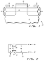
- FIG. 1 illustrates an embodiment of a MOSFET device 10 having enhanced carrier mobility according to the present invention.
- Carrier transport region or channel layer 12 is formed on a monocrystalline silicon layer 11.
- Channel layer 12 comprises an alloy of silicon and a second material.
- Monocrystalline silicon layer 11 has an n-type conductivity for p-channel devices and a p-type conductivity for n-channel devices.
- the second material is substitutionally present in channel layer 12 lattice sites and is present at an atomic percentage such that channel layer 12 is under a tensile stress compared to monocrystalline silicon layer 11 or a crystal consisting of silicon.
- channel layer 12 is not doped with acceptor or donor impurities.
- MOSFET device 10 further comprises epitaxial semiconductor or epitaxial layer 13 formed over channel layer 12.
- epitaxial layer 13 comprises silicon and is on the order of 50 angstroms thick.
- a source region 14 and a drain region 16 extend through epitaxial layer 13 and at least into channel layer 12.
- source region 14 and drain region 16 extend through channel layer 12 into monocrystalline silicon layer 11.
- a portion of channel layer 12 is between source region 14 and drain region 16.
- a control or gate electrode 18 is electrically insulated from epitaxial layer 13.
- gate electrode 18 is electrically insulated from epitaxial layer 13 with gate dielectric layer 17.
- Gate dielectric layer 17 preferably comprises an oxide and has a thickness in the range from 30 to 125 angstroms.
- a source electrode 19 is formed on a portion of source region 14 and a drain electrode 21 is formed on a portion of drain region 16.
- FIG. 2 is an energy band diagram of the embodiment of FIG. 1 under a zero gate bias and illustrates the effect of strain induced band splitting on channel layer 12.
- FIG. 2 shows the relative relationship between valence band 22 and conduction band 23 in epitaxial layer 13, channel layer 12, and monocrystalline silicon layer 11.
- valence band edge or interface 24 in channel layer 12 splits and in effect, moves up in energy level toward conduction band 23.
- conduction band edge or interface 26 splits and in effect, moves down in energy level toward valence band 22. This results in a channel layer bandgap 27 that is narrower than monocrystalline silicon layer bandgap 28 and epitaxial layer bandgap 29.
- channel layer bandgap 27 in effect creates a potential well that traps holes and electrons within channel layer 12. Also, the above effect results in channel layer 12 having energy levels preferentially populated with holes and electrons with reduced effective carrier masses. This in turn enhances free carrier mobility in channel layer 12 when the appropriate gate bias is applied to gate electrode 18.
- a channel layer under tensile stress is preferred over a channel layer under compressive stress because tensile stress provides greater conduction band splitting.
- lower effective carrier masses are predicted with films under tensile stress compared to films under compressive stress.
- a channel layer under tensile stress provides enhanced mobility for both electron and hole carriers and supports the fabrication of enhanced mobility complementary p-channel and n-channel devices.
- carbon-doped silicon is an alloy or material that is suitable for channel layer 12.
- channel layer 12 comprises a carbon-doped silicon or Si 1-X C X alloy where carbon is the second material, the carbon is present in substitutional silicon lattice sites, and X preferably is less than or equal to 0.02.
- X is in the range of approximately 0.005 and 0.016.
- channel layer 12 has a thickness on the order of 100 to 200 angstroms when X is on the order of 0.02 to 0.005 respectively.
- the thickness of channel layer 12 is adjusted according to the atomic percentage of carbon present.
- epitaxial layer 13 preferably comprises silicon and has a thickness in the range from 50 to 100 angstroms.
- a carbon-doped silicon channel layer is preferred over a germanium-doped silicon channel layer because a carbon-doped channel layer has a lower alloy/carrier scattering effect. This is because the relative size difference between carbon and germanium atoms allows one to use a much reduced (on the order of 11 to 1) amount of carbon compared to germanium to achieve similar strain magnitudes (although opposite in sign). Because a carbon-doped silicon channel layer has a reduced alloy/carrier scattering effect compared to a similarly strained germanium-doped silicon channel layer, carrier mobility, particularly electron mobility, is additionally enhanced. Furthermore, because channel layer 12 in MOSFET device 10 is buried, that is, bounded by epitaxial layer 13 and monocrystalline silicon layer 11, MOSFET device 10 is less susceptible to surface scattering, hot carrier degradation, and noise effects.
- channel layer 12 comprises a Si 1-X C X alloy
- epitaxial growth or chemical vapor deposition techniques are used to form channel layer 12.
- An acetylene, ethylene, propane, or methane carbon source is used, for example.
- a silicon layer is formed, carbon is ion implanted into the silicon layer, and the carbon-doped silicon layer is heated to induce solid phase epitaxial regrowth of the carbon-doped silicon layer to form channel layer 12.
- molecular beam epitaxy, metallo organic chemical vapor deposition (MOCVD), or ultra-high vacuum chemical vapor deposition (UHVCVD) is used to form channel layer 12.
- MOSFET device 10 having a p-channel configuration and a carbon-doped channel layer
- monocrystalline silicon layer 11 having an n-type conductivity is selectively formed on or in a p-type substrate.
- Channel layer 12 comprising carbon-doped silicon is then formed over the undoped silicon layer.
- epitaxial layer 13 comprising either n-type doped or undoped silicon and having a thickness on the order of 50 to 100 angstroms is formed over channel layer 12.
- the undoped silicon layer, channel layer 12, and epitaxial layer 13 are formed in a single epitaxial growth step.
- a silicon oxide layer having a thickness in the range from 60 to 80 angstroms is then deposited or grown on epitaxial layer 13.
- an in-situ doped n-type polysilicon layer is formed over the silicon oxide layer.
- the n-type polysilicon layer and the silicon oxide layer are then selectively patterned to form gate electrode 18 and gate dielectric layer 17 respectively.
- p-type dopant is selectively incorporated into epitaxial layer 13.
- the structure is then heated to activate the p-type dopant to form source region 14 and drain region 16.
- Standard MOSFET processing is then used to complete MOSFET device 10.
- MOSFET device 10 In an n-channel configuration, the dopant conductivity types are reversed.
- FIGS. 3-5 illustrate alternative embodiments of an enhanced mobility MOSFET device according to the present invention.
- MOSFET device 30 shown in FIG. 3 is similar to MOSFET device 10 except MOSFET device 30 does not have epitaxial layer 13.
- MOSFET device 30 has an enhanced mobility as described above but is more susceptible to surface scattering effects because of the interface between channel layer 12 and gate dielectric layer 17. However, the carrier mobility of MOSFET device 30 is still enhanced when compared to a similarly constructed non-stressed silicon channel MOSFET device.
- MOSFET device 40 shown in FIG. 4 is similar to MOSFET device 10 with the addition of modulation doping or modulation layer 41 formed within monocrystalline silicon layer 11.
- a portion 43 of monocrystalline silicon layer 11 separates modulation layer 41 from channel layer 12.
- Portion 43 preferably has a thickness on the order of 50 to 100 angstroms.
- Modulation layer 41 is of the same conductivity type as source region 14 and drain region 16.
- Modulation layer 41 has a higher dopant concentration than the dopant concentration of monocrystalline silicon layer 11 and is of an opposite conductivity type than monocrystalline silicon layer 11.
- modulation layer 41 has a thickness in the range from 100 to 200 angstroms.
- Modulation layer 41 is formed on portion 42 of monocrystalline silicon layer 11 using epitaxial growth or chemical vapor deposition (CVD) techniques. Portion 43 of monocrystalline silicon layer 11 is then formed on modulation layer 41 using epitaxial growth or CVD techniques. Portion 43 of monocrystalline silicon layer 11 can be doped n or p-type by using ion implantation and/or diffusion techniques, depending upon whether MOSFET device 40 is a p-channel or an n-channel device respectively. Preferably, modulation layer 41 and portion 43 of monocrystalline silicon layer 11 are formed sequentially in a single in-situ process sequence.
- MOSFET device 50 shown in FIG. 5 is similar to MOSFET device 10 with the addition of insulating layer or region 51 to form a semiconductor-on-insulator (IIIII) device.
- Insulating layer 51 preferably comprises silicon oxide and is formed using oxygen ion implantation or other techniques. Insulating layer 51 preferably is formed before channel layer 12 and epitaxial layer 13 are formed. Alternatively, insulating layer 51 is formed on a supporting substrate (not shown), a monocrystalline silicon substrate is then bonded to insulating layer 51, and the monocrystalline silicon substrate is thinned to the desired thickness to form monocrystalline silicon layer 11.
- insulating layer 51 is spaced a distance 52 of 500 to 600 angstroms from channel layer 12.
- insulating layer 51 When insulating layer 51 is used with MOSFET device 30 (FIG. 3), insulating layer 51 preferably is spaced on the order of 1000 angstroms below channel layer 12. When insulating layer 51 is used with MOSFET device 40 (FIG. 4), insulating layer 51 preferably is spaced on the order of 100 to 200 angstroms below modulation layer 41.
- an enhanced mobility MOSFET device By forming a carrier transport region on a monocrystalline silicon layer, where the carrier transport region comprises an alloy of silicon and a second material, and where the second material is present in the carrier transport region at an atomic percentage that places the carrier transport region under a tensile stress, enhanced carrier mobility is achieved.
- a buried structure is provided that is less susceptible to surface scattering, hot carrier degradation, and noise effects.
- the carrier transport region comprises carbon-doped silicon
- reduced alloy scattering is achieved compared to similarly strained carrier regions comprising germanium-doped silicon.
- the carrier transport region comprises carbon-doped silicon
- a carrier transport region under tensile stress is achieved without using a relaxed alloy layer. This reduces process complexity and costs.
Abstract
Description
- This invention relates, in general, to semiconductor devices, and more particularly, to semiconductor devices having enhanced carrier mobility.
- Metal oxide semiconductor field effect transistor (MOSFET) devices are well known and widely used in the electronics industry. The carrier mobility of a MOSFET device is an important parameter because of its direct influence on output current and switching performance. In standard MOSFET technology, the channel length and gate dielectric thickness are reduced to improve current drive and switching performance. However, reducing the gate dielectric thickness can compromise device performance because of the associated increase in intrinsic gate capacitance.
- In silicon MOSFET devices, it has been shown that a buried channel region under compressive stress consisting of a silicon/germanium (Si1-XGeX) alloy, bounded above and below by silicon regions, enhances hole carrier mobility in the channel region. This is because the holes are confined to the channel region by the potential energy offset between the surrounding silicon regions and the Si1-XGeX channel region. Such strained devices are shown in U.S. Patent No. 5,241,197 issued to Murakami et al., and U.S. Patent No. 5,241,197 issued to Solomon et al.
- Buried Si1-XGeX channel devices have several disadvantages including increased alloy scattering in the channel region that degrades electron mobility, no favorable conduction band offset thus minimally enhanced electron mobility, no higher carrier velocities than silicon, and the need for large Ge concentrations to produce strain and thus enhanced mobility. Large Ge concentrations result in greatly reduced layer thicknesses and processing temperatures. The reduced processing temperatures adversely affect dopant activation and gate oxide processing.
- Silicon devices with channel regions under a tensile stress are desirable because the tensile strain results in both hole and electron mobility enhancement and increased carrier velocity compared to silicon. One reported approach uses a strained silicon surface channel region with a relaxed Si0.7Ge0.3 alloy layer below the silicon channel region and a Si1-XGeX (X=5-30%) buffer layer below the Si0.7Ge0.3 alloy layer. One advantage of this approach is the elimination of alloy scattering in the channel region. However, this approach has a disadvantage in that the strained channel layer is at the surface and is thus susceptible to surface scattering effects that reduce mobility. It is also susceptible to hot carrier degradation and noise problems. In addition, the approach requires alloy relaxing and buffering layers, which increases process complexity and costs.
- Another reported approach uses a strained Si1-XGeX channel layer formed on a relaxed Si1-YGeY layer (where Y>X) with a silicon layer above the strained Si1-XGeX channel layer and a silicon layer below the relaxed Si1-YGeY layer. This structure has several disadvantages including the migration of carriers out of the strained Si1-XGeX channel layer into the relaxed Si1-YGeY alloy layer thus reducing the enhanced mobility effect, greater alloy scattering effects because of the presence of germanium in the channel layer, and added process complexity because of multiple SiGe layers.
- As is readily apparent, there exists a need for a MOSFET device that has enhanced electron and hole mobility, that is less susceptible to alloy scattering effects, that is less susceptible to surface scattering effects, and that does not require alloy relaxing and/or buffering layers.
- Briefly stated, an enhanced mobility MOSFET device comprises a carrier transport region formed on a monocrystalline silicon layer of a first conductivity type. The carrier transport region comprises an alloy of silicon and a second material, wherein the second material is present in the carrier transport region at an atomic percentage such that the carrier transport region is under tensile stress. A source region and a drain region of a second conductivity type extend into the carrier transport region. A portion of the carrier transport region separates the source region and the drain region. A control electrode is electrically insulated from the carrier transport region and is disposed between the source region and the drain region.
- A method for making an enhanced mobility MOSFET described herein comprises forming a carrier transport region on a first conductivity type monocrystalline silicon layer. The carrier transport layer comprises an alloy of silicon and a second material. The second material is present in the carrier transport region at an atomic percentage that places the carrier transport region under tensile stress. A gate dielectric layer is formed on a portion of the carrier transport region. A control electrode is formed on the gate dielectric layer. A source region and a drain region having a second conductivity type are formed such that they extend at least into the carrier transport region and the portion of the carrier transport region is between the source and drain regions.
-
- FIG. 1 is an enlarged sectional view of an embodiment of the present invention;
- FIG. 2 is an energy band diagram of the embodiment of FIG. 1 under zero gate bias;
- FIG. 3 is an enlarged sectional view of another embodiment of the present invention;
- FIG. 4 is an enlarged sectional view of an additional embodiment of the present invention; and
- FIG. 5 is an enlarged sectional view of a further embodiment of the present invention.
- FIG. 1 illustrates an embodiment of a
MOSFET device 10 having enhanced carrier mobility according to the present invention. Carrier transport region orchannel layer 12 is formed on amonocrystalline silicon layer 11.Channel layer 12 comprises an alloy of silicon and a second material.Monocrystalline silicon layer 11 has an n-type conductivity for p-channel devices and a p-type conductivity for n-channel devices. The second material is substitutionally present inchannel layer 12 lattice sites and is present at an atomic percentage such thatchannel layer 12 is under a tensile stress compared tomonocrystalline silicon layer 11 or a crystal consisting of silicon. Preferably,channel layer 12 is not doped with acceptor or donor impurities. -
MOSFET device 10 further comprises epitaxial semiconductor orepitaxial layer 13 formed overchannel layer 12. Preferably,epitaxial layer 13 comprises silicon and is on the order of 50 angstroms thick. Asource region 14 and adrain region 16 extend throughepitaxial layer 13 and at least intochannel layer 12. Preferably,source region 14 anddrain region 16 extend throughchannel layer 12 intomonocrystalline silicon layer 11. A portion ofchannel layer 12 is betweensource region 14 and drainregion 16. A control orgate electrode 18 is electrically insulated fromepitaxial layer 13. Preferably,gate electrode 18 is electrically insulated fromepitaxial layer 13 with gatedielectric layer 17. Gatedielectric layer 17 preferably comprises an oxide and has a thickness in the range from 30 to 125 angstroms. Asource electrode 19 is formed on a portion ofsource region 14 and adrain electrode 21 is formed on a portion ofdrain region 16. - FIG. 2 is an energy band diagram of the embodiment of FIG. 1 under a zero gate bias and illustrates the effect of strain induced band splitting on
channel layer 12. FIG. 2 shows the relative relationship betweenvalence band 22 andconduction band 23 inepitaxial layer 13,channel layer 12, andmonocrystalline silicon layer 11. Whenchannel layer 12 is under tensile stress, valence band edge orinterface 24 inchannel layer 12 splits and in effect, moves up in energy level towardconduction band 23. In addition, conduction band edge orinterface 26 splits and in effect, moves down in energy level towardvalence band 22. This results in achannel layer bandgap 27 that is narrower than monocrystallinesilicon layer bandgap 28 andepitaxial layer bandgap 29. The offset or narrowing of channel layer bandgap 27 in effect creates a potential well that traps holes and electrons withinchannel layer 12. Also, the above effect results inchannel layer 12 having energy levels preferentially populated with holes and electrons with reduced effective carrier masses. This in turn enhances free carrier mobility inchannel layer 12 when the appropriate gate bias is applied togate electrode 18. - A channel layer under tensile stress is preferred over a channel layer under compressive stress because tensile stress provides greater conduction band splitting. In addition, lower effective carrier masses are predicted with films under tensile stress compared to films under compressive stress. Thus, a channel layer under tensile stress provides enhanced mobility for both electron and hole carriers and supports the fabrication of enhanced mobility complementary p-channel and n-channel devices.
- As shown in U.S. Patent No. 5,360,986, issued to J. Candelaria and assigned to Motorola Inc., hereby incorporated herein by reference, carbon-doped silicon is an alloy or material that is suitable for
channel layer 12. In a preferred embodiment,channel layer 12 comprises a carbon-doped silicon or Si1-XCX alloy where carbon is the second material, the carbon is present in substitutional silicon lattice sites, and X preferably is less than or equal to 0.02. Preferably, X is in the range of approximately 0.005 and 0.016. - Preferably,
channel layer 12 has a thickness on the order of 100 to 200 angstroms when X is on the order of 0.02 to 0.005 respectively. The thickness ofchannel layer 12 is adjusted according to the atomic percentage of carbon present. Whenchannel layer 12 comprises a Si1-XCX alloy,epitaxial layer 13 preferably comprises silicon and has a thickness in the range from 50 to 100 angstroms. - A carbon-doped silicon channel layer is preferred over a germanium-doped silicon channel layer because a carbon-doped channel layer has a lower alloy/carrier scattering effect. This is because the relative size difference between carbon and germanium atoms allows one to use a much reduced (on the order of 11 to 1) amount of carbon compared to germanium to achieve similar strain magnitudes (although opposite in sign). Because a carbon-doped silicon channel layer has a reduced alloy/carrier scattering effect compared to a similarly strained germanium-doped silicon channel layer, carrier mobility, particularly electron mobility, is additionally enhanced. Furthermore, because
channel layer 12 inMOSFET device 10 is buried, that is, bounded byepitaxial layer 13 andmonocrystalline silicon layer 11,MOSFET device 10 is less susceptible to surface scattering, hot carrier degradation, and noise effects. - When
channel layer 12 comprises a Si1-XCX alloy, epitaxial growth or chemical vapor deposition techniques are used to formchannel layer 12. An acetylene, ethylene, propane, or methane carbon source is used, for example. Alternatively, as shown in U.S. Patent No. 5,360,986, a silicon layer is formed, carbon is ion implanted into the silicon layer, and the carbon-doped silicon layer is heated to induce solid phase epitaxial regrowth of the carbon-doped silicon layer to formchannel layer 12. Alternatively, molecular beam epitaxy, metallo organic chemical vapor deposition (MOCVD), or ultra-high vacuum chemical vapor deposition (UHVCVD) is used to formchannel layer 12. - In a preferred embodiment for forming
MOSFET device 10 having a p-channel configuration and a carbon-doped channel layer,monocrystalline silicon layer 11 having an n-type conductivity is selectively formed on or in a p-type substrate.Channel layer 12 comprising carbon-doped silicon is then formed over the undoped silicon layer. Next,epitaxial layer 13 comprising either n-type doped or undoped silicon and having a thickness on the order of 50 to 100 angstroms is formed overchannel layer 12. Preferably, the undoped silicon layer,channel layer 12, andepitaxial layer 13 are formed in a single epitaxial growth step. - A silicon oxide layer having a thickness in the range from 60 to 80 angstroms is then deposited or grown on
epitaxial layer 13. Next, an in-situ doped n-type polysilicon layer is formed over the silicon oxide layer. The n-type polysilicon layer and the silicon oxide layer are then selectively patterned to formgate electrode 18 andgate dielectric layer 17 respectively. Next, p-type dopant is selectively incorporated intoepitaxial layer 13. The structure is then heated to activate the p-type dopant to formsource region 14 and drainregion 16. Standard MOSFET processing is then used to completeMOSFET device 10. Toform MOSFET device 10 in an n-channel configuration, the dopant conductivity types are reversed. - FIGS. 3-5 illustrate alternative embodiments of an enhanced mobility MOSFET device according to the present invention.
MOSFET device 30 shown in FIG. 3 is similar toMOSFET device 10 exceptMOSFET device 30 does not haveepitaxial layer 13.MOSFET device 30 has an enhanced mobility as described above but is more susceptible to surface scattering effects because of the interface betweenchannel layer 12 andgate dielectric layer 17. However, the carrier mobility ofMOSFET device 30 is still enhanced when compared to a similarly constructed non-stressed silicon channel MOSFET device. -
MOSFET device 40 shown in FIG. 4 is similar toMOSFET device 10 with the addition of modulation doping ormodulation layer 41 formed withinmonocrystalline silicon layer 11. Aportion 43 ofmonocrystalline silicon layer 11separates modulation layer 41 fromchannel layer 12.Portion 43 preferably has a thickness on the order of 50 to 100 angstroms.Modulation layer 41 is of the same conductivity type assource region 14 and drainregion 16.Modulation layer 41 has a higher dopant concentration than the dopant concentration ofmonocrystalline silicon layer 11 and is of an opposite conductivity type thanmonocrystalline silicon layer 11. Preferably,modulation layer 41 has a thickness in the range from 100 to 200 angstroms. -
Modulation layer 41 is formed onportion 42 ofmonocrystalline silicon layer 11 using epitaxial growth or chemical vapor deposition (CVD) techniques.Portion 43 ofmonocrystalline silicon layer 11 is then formed onmodulation layer 41 using epitaxial growth or CVD techniques.Portion 43 ofmonocrystalline silicon layer 11 can be doped n or p-type by using ion implantation and/or diffusion techniques, depending upon whetherMOSFET device 40 is a p-channel or an n-channel device respectively. Preferably,modulation layer 41 andportion 43 ofmonocrystalline silicon layer 11 are formed sequentially in a single in-situ process sequence. -
MOSFET device 50 shown in FIG. 5 is similar toMOSFET device 10 with the addition of insulating layer orregion 51 to form a semiconductor-on-insulator (IIIII) device. Insulatinglayer 51 preferably comprises silicon oxide and is formed using oxygen ion implantation or other techniques. Insulatinglayer 51 preferably is formed beforechannel layer 12 andepitaxial layer 13 are formed. Alternatively, insulatinglayer 51 is formed on a supporting substrate (not shown), a monocrystalline silicon substrate is then bonded to insulatinglayer 51, and the monocrystalline silicon substrate is thinned to the desired thickness to formmonocrystalline silicon layer 11. Preferably, insulatinglayer 51 is spaced adistance 52 of 500 to 600 angstroms fromchannel layer 12. - When insulating
layer 51 is used with MOSFET device 30 (FIG. 3), insulatinglayer 51 preferably is spaced on the order of 1000 angstroms belowchannel layer 12. When insulatinglayer 51 is used with MOSFET device 40 (FIG. 4), insulatinglayer 51 preferably is spaced on the order of 100 to 200 angstroms belowmodulation layer 41. - By now it should be appreciated that there has been provided an enhanced mobility MOSFET device. By forming a carrier transport region on a monocrystalline silicon layer, where the carrier transport region comprises an alloy of silicon and a second material, and where the second material is present in the carrier transport region at an atomic percentage that places the carrier transport region under a tensile stress, enhanced carrier mobility is achieved.
- Also, by placing the carrier transport region under tensile stress, greater conduction band splitting is achieved compared to a carrier transport region under compressive stress thus providing enhanced mobility for both electron and hole carriers. This supports the fabrication of enhanced mobility complementary n-channel and p-channel devices.
- In addition, by adding an epitaxial layer over the carrier transport region, a buried structure is provided that is less susceptible to surface scattering, hot carrier degradation, and noise effects.
- Furthermore, when the carrier transport region comprises carbon-doped silicon, reduced alloy scattering is achieved compared to similarly strained carrier regions comprising germanium-doped silicon. Also, when the carrier transport region comprises carbon-doped silicon, a carrier transport region under tensile stress is achieved without using a relaxed alloy layer. This reduces process complexity and costs.
Claims (10)
- An enhanced mobility MOSFET device comprising:
a monocrystalline silicon layer (11) of a first conductivity type;
a carrier transport region (12) formed on the monocrystalline silicon layer (11), wherein the carrier transport region (12) comprises an alloy of silicon and a second semiconductor material, and wherein the second semiconductor material is substitutionally present in carrier transport region (12) lattice sites at an atomic percentage such that the carrier transport region is under tensile stress;
a source region (14) of a second conductivity type extending into the carrier transport region (12);
a drain region (16) of the second conductivity type extending into the carrier transport region (12), wherein a portion of the carrier transport region (12) is between the source region (14) and the drain region (16); and
a control electrode (18) electrically insulated from the carrier transport region (12), wherein the control electrode (18) is disposed between the source region (14) and the drain region (16). - The device of claim 1 further comprising:
an epitaxial layer (13) of the first semiconductor material disposed between the carrier transport region (12) and the control electrode (18), wherein the source region (14) and the drain region (16) extend through the epitaxial layer (13) into at least the carrier transport region (12). - The device of claim 1 wherein the carrier transport region (12) comprises a Si1-XCX alloy.
- The device of claim 3 wherein X is less than or equal to 0.02.
- A MOSFET structure having a buried carbon-doped silicon channel region comprising:
a channel layer (12) comprises a Si1-XCX alloy formed on a monocrystalline silicon layer (11) of a first conductivity type, wherein carbon is present in the channel layer (12) in substitutional lattice sites so that the channel layer (12) is under tensile stress;
an epitaxial silicon layer (13) formed on the channel layer;
a source region (14) of a second conductivity type extending through the epitaxial silicon layer (13) and at least into the channel layer (12);
a drain region (16) of the second conductivity type extending through the epitaxial silicon layer (13) and at least into the channel layer (12), wherein part of the channel layer (12) separates the source region (14) from the drain region (16);
a gate dielectric layer (17) formed on the epitaxial silicon layer (13) at least between the source region (14) and the drain region (16); and
a gate electrode (18) formed on the gate dielectric layer (17). - The structure of claim 5 wherein X is less than or equal to 0.02, and wherein the monocrystalline silicon layer (11) has a thickness on an order of 1000 angstroms, the channel layer (12) has a thickness on an order of 100 angstroms, and the epitaxial silicon layer (13) has a thickness on an order of 50 angstroms.
- The structure of claim 5 further comprising an insulating region (51) disposed below the monocrystalline silicon layer (11).
- The structure of claim 5 wherein the monocrystalline silicon layer (11) includes a modulation layer (41) disposed within the monocrystalline silicon layer (11), wherein a portion of the monocrystalline silicon layer (11) separates the modulation layer (41) from the channel layer (21), and wherein the modulation layer (41) is of the second conductivity type, and wherein the modulation layer (41) has a dopant concentration that is higher than dopant concentration in the monocrystalline silicon layer (11).
- A method for making an enhanced mobility MOSFET device comprising the steps of:
forming a carrier transport region (12) on a first conductivity type monocrystalline silicon layer (11), wherein the carrier transport region (12) comprises an alloy of the silicon and a second semiconductor material, and wherein the second semiconductor material is substitutionally present in carrier transport region (12) lattice sites at an atomic percentage that places the carrier transport region (12) under tensile stress compared to the first conductivity type monocrystalline silicon layer (11);
forming an epitaxial semiconductor layer (13) over the carrier transport region (12);
forming a gate dielectric layer (17) on the epitaxial semiconductor layer (13) above a portion of the carrier transport layer (12);
forming a control electrode (18) on the gate dielectric layer (17);
forming a source region (14) of a second conductivity type extending through the epitaxial semiconductor layer (13) at least into the carrier transport region (12); and
forming a drain region (16) of the second conductivity type extending through the epitaxial semiconductor layer (13) at least into the carrier transport region (12), wherein the portion of the carrier transport region (12) is between the source region (14) and the drain region (16). - The method of claim 9 wherein the step of forming the carrier transport region (12) includes forming a carrier transport region (12) comprising a Si1-XCX alloy, wherein X is less than or equal to 0.02.
Applications Claiming Priority (2)
| Application Number | Priority Date | Filing Date | Title |
|---|---|---|---|
| US08/311,979 US5561302A (en) | 1994-09-26 | 1994-09-26 | Enhanced mobility MOSFET device and method |
| US311979 | 1994-09-26 |
Publications (2)
| Publication Number | Publication Date |
|---|---|
| EP0703628A2 true EP0703628A2 (en) | 1996-03-27 |
| EP0703628A3 EP0703628A3 (en) | 1997-05-14 |
Family
ID=23209323
Family Applications (1)
| Application Number | Title | Priority Date | Filing Date |
|---|---|---|---|
| EP95114228A Withdrawn EP0703628A3 (en) | 1994-09-26 | 1995-09-11 | Enhanced mobility MOSFET device and method |
Country Status (5)
| Country | Link |
|---|---|
| US (2) | US5561302A (en) |
| EP (1) | EP0703628A3 (en) |
| JP (1) | JPH08111528A (en) |
| KR (1) | KR960012557A (en) |
| CN (1) | CN1129358A (en) |
Cited By (8)
| Publication number | Priority date | Publication date | Assignee | Title |
|---|---|---|---|---|
| EP0829908A2 (en) * | 1996-09-17 | 1998-03-18 | Matsushita Electric Industrial Co., Ltd. | Field-effect transistor and method of producing the same |
| EP0921575A2 (en) * | 1997-12-03 | 1999-06-09 | Matsushita Electric Industrial Co., Ltd. | Semiconductor device comprising a heterostructure MIS field-effect transistor having a strained channel layer |
| WO2002045156A2 (en) * | 2000-11-29 | 2002-06-06 | Intel Corporation | Cmos fabrication process utilizing special transistor orientation |
| US6657276B1 (en) * | 2001-12-10 | 2003-12-02 | Advanced Micro Devices, Inc. | Shallow trench isolation (STI) region with high-K liner and method of formation |
| WO2005043590A2 (en) | 2003-10-20 | 2005-05-12 | International Business Machines Corporation | Strained dislocation-free channels for cmos and method of manufacture |
| EP1928013A3 (en) * | 2006-12-01 | 2010-06-23 | Applied Materials, Inc. | Formation and treatment of epitaxial layer containing silicon and carbon |
| US7888710B2 (en) | 2000-11-29 | 2011-02-15 | Intel Corporation | CMOS fabrication process utilizing special transistor orientation |
| US8017489B2 (en) | 2008-03-13 | 2011-09-13 | International Business Machines Corporation | Field effect structure including carbon alloyed channel region and source/drain region not carbon alloyed |
Families Citing this family (323)
| Publication number | Priority date | Publication date | Assignee | Title |
|---|---|---|---|---|
| JPH07321323A (en) | 1994-05-24 | 1995-12-08 | Matsushita Electric Ind Co Ltd | Thin film transistor and its manufacturing method |
| JP3243146B2 (en) * | 1994-12-08 | 2002-01-07 | 株式会社東芝 | Semiconductor device |
| JP3305197B2 (en) * | 1995-09-14 | 2002-07-22 | 株式会社東芝 | Semiconductor device |
| JP2839018B2 (en) * | 1996-07-31 | 1998-12-16 | 日本電気株式会社 | Method for manufacturing semiconductor device |
| JP3461274B2 (en) * | 1996-10-16 | 2003-10-27 | 株式会社東芝 | Semiconductor device |
| JPH10270685A (en) | 1997-03-27 | 1998-10-09 | Sony Corp | Field-effect transistor and manufacture thereof, semiconductor device and manufacture thereof and logic circuit containing semiconductor device thereof and semiconductor substrate |
| US5891769A (en) * | 1997-04-07 | 1999-04-06 | Motorola, Inc. | Method for forming a semiconductor device having a heteroepitaxial layer |
| JP3535527B2 (en) | 1997-06-24 | 2004-06-07 | マサチューセッツ インスティテュート オブ テクノロジー | Controlling threading dislocations in germanium-on-silicon using graded GeSi layer and planarization |
| US7227176B2 (en) | 1998-04-10 | 2007-06-05 | Massachusetts Institute Of Technology | Etch stop layer system |
| EP1020900B1 (en) * | 1999-01-14 | 2009-08-05 | Panasonic Corporation | Semiconductor device and method for fabricating the same |
| US6350993B1 (en) | 1999-03-12 | 2002-02-26 | International Business Machines Corporation | High speed composite p-channel Si/SiGe heterostructure for field effect devices |
| US6281532B1 (en) * | 1999-06-28 | 2001-08-28 | Intel Corporation | Technique to obtain increased channel mobilities in NMOS transistors by gate electrode engineering |
| US6656822B2 (en) | 1999-06-28 | 2003-12-02 | Intel Corporation | Method for reduced capacitance interconnect system using gaseous implants into the ILD |
| EP1102327B1 (en) * | 1999-11-15 | 2007-10-03 | Matsushita Electric Industrial Co., Ltd. | Field effect semiconductor device |
| US6602613B1 (en) | 2000-01-20 | 2003-08-05 | Amberwave Systems Corporation | Heterointegration of materials using deposition and bonding |
| US6750130B1 (en) | 2000-01-20 | 2004-06-15 | Amberwave Systems Corporation | Heterointegration of materials using deposition and bonding |
| US6503773B2 (en) | 2000-01-20 | 2003-01-07 | Amberwave Systems Corporation | Low threading dislocation density relaxed mismatched epilayers without high temperature growth |
| DE10025264A1 (en) * | 2000-05-22 | 2001-11-29 | Max Planck Gesellschaft | Field effect transistor based on embedded cluster structures and method for its production |
| WO2001093338A1 (en) * | 2000-05-26 | 2001-12-06 | Amberwave Systems Corporation | Buried channel strained silicon fet using an ion implanted doped layer |
| US6743680B1 (en) * | 2000-06-22 | 2004-06-01 | Advanced Micro Devices, Inc. | Process for manufacturing transistors having silicon/germanium channel regions |
| US6461945B1 (en) | 2000-06-22 | 2002-10-08 | Advanced Micro Devices, Inc. | Solid phase epitaxy process for manufacturing transistors having silicon/germanium channel regions |
| JP2004519090A (en) * | 2000-08-07 | 2004-06-24 | アンバーウェーブ システムズ コーポレイション | Gate technology for strained surface channel and strained buried channel MOSFET devices |
| US6521502B1 (en) | 2000-08-07 | 2003-02-18 | Advanced Micro Devices, Inc. | Solid phase epitaxy activation process for source/drain junction extensions and halo regions |
| US6573126B2 (en) | 2000-08-16 | 2003-06-03 | Massachusetts Institute Of Technology | Process for producing semiconductor article using graded epitaxial growth |
| US6544854B1 (en) * | 2000-11-28 | 2003-04-08 | Lsi Logic Corporation | Silicon germanium CMOS channel |
| US6649480B2 (en) | 2000-12-04 | 2003-11-18 | Amberwave Systems Corporation | Method of fabricating CMOS inverter and integrated circuits utilizing strained silicon surface channel MOSFETs |
| US20020100942A1 (en) * | 2000-12-04 | 2002-08-01 | Fitzgerald Eugene A. | CMOS inverter and integrated circuits utilizing strained silicon surface channel MOSFETs |
| US6844227B2 (en) * | 2000-12-26 | 2005-01-18 | Matsushita Electric Industrial Co., Ltd. | Semiconductor devices and method for manufacturing the same |
| US6495402B1 (en) | 2001-02-06 | 2002-12-17 | Advanced Micro Devices, Inc. | Semiconductor-on-insulator (SOI) device having source/drain silicon-germanium regions and method of manufacture |
| US6380590B1 (en) | 2001-02-22 | 2002-04-30 | Advanced Micro Devices, Inc. | SOI chip having multiple threshold voltage MOSFETs by using multiple channel materials and method of fabricating same |
| US6475869B1 (en) | 2001-02-26 | 2002-11-05 | Advanced Micro Devices, Inc. | Method of forming a double gate transistor having an epitaxial silicon/germanium channel region |
| US6410371B1 (en) | 2001-02-26 | 2002-06-25 | Advanced Micro Devices, Inc. | Method of fabrication of semiconductor-on-insulator (SOI) wafer having a Si/SiGe/Si active layer |
| US6830976B2 (en) | 2001-03-02 | 2004-12-14 | Amberwave Systems Corproation | Relaxed silicon germanium platform for high speed CMOS electronics and high speed analog circuits |
| US6900103B2 (en) | 2001-03-02 | 2005-05-31 | Amberwave Systems Corporation | Relaxed silicon germanium platform for high speed CMOS electronics and high speed analog circuits |
| US6724008B2 (en) | 2001-03-02 | 2004-04-20 | Amberwave Systems Corporation | Relaxed silicon germanium platform for high speed CMOS electronics and high speed analog circuits |
| US6723661B2 (en) | 2001-03-02 | 2004-04-20 | Amberwave Systems Corporation | Relaxed silicon germanium platform for high speed CMOS electronics and high speed analog circuits |
| US6593641B1 (en) | 2001-03-02 | 2003-07-15 | Amberwave Systems Corporation | Relaxed silicon germanium platform for high speed CMOS electronics and high speed analog circuits |
| US6703688B1 (en) | 2001-03-02 | 2004-03-09 | Amberwave Systems Corporation | Relaxed silicon germanium platform for high speed CMOS electronics and high speed analog circuits |
| US6677192B1 (en) | 2001-03-02 | 2004-01-13 | Amberwave Systems Corporation | Method of fabricating a relaxed silicon germanium platform having planarizing for high speed CMOS electronics and high speed analog circuits |
| US6646322B2 (en) | 2001-03-02 | 2003-11-11 | Amberwave Systems Corporation | Relaxed silicon germanium platform for high speed CMOS electronics and high speed analog circuits |
| US6709935B1 (en) | 2001-03-26 | 2004-03-23 | Advanced Micro Devices, Inc. | Method of locally forming a silicon/geranium channel layer |
| US6921743B2 (en) * | 2001-04-02 | 2005-07-26 | The Procter & Gamble Company | Automatic dishwashing compositions containing a halogen dioxide salt and methods for use with electrochemical cells and/or electrolytic devices |
| WO2002082514A1 (en) | 2001-04-04 | 2002-10-17 | Massachusetts Institute Of Technology | A method for semiconductor device fabrication |
| US6750119B2 (en) * | 2001-04-20 | 2004-06-15 | International Business Machines Corporation | Epitaxial and polycrystalline growth of Si1-x-yGexCy and Si1-yCy alloy layers on Si by UHV-CVD |
| AU2002322105A1 (en) * | 2001-06-14 | 2003-01-02 | Amberware Systems Corporation | Method of selective removal of sige alloys |
| US7301180B2 (en) | 2001-06-18 | 2007-11-27 | Massachusetts Institute Of Technology | Structure and method for a high-speed semiconductor device having a Ge channel layer |
| US6916727B2 (en) * | 2001-06-21 | 2005-07-12 | Massachusetts Institute Of Technology | Enhancement of P-type metal-oxide-semiconductor field effect transistors |
| US6730551B2 (en) | 2001-08-06 | 2004-05-04 | Massachusetts Institute Of Technology | Formation of planar strained layers |
| US6974735B2 (en) * | 2001-08-09 | 2005-12-13 | Amberwave Systems Corporation | Dual layer Semiconductor Devices |
| US7138649B2 (en) | 2001-08-09 | 2006-11-21 | Amberwave Systems Corporation | Dual-channel CMOS transistors with differentially strained channels |
| KR100425462B1 (en) * | 2001-09-10 | 2004-03-30 | 삼성전자주식회사 | Semiconductor device on SOI(silicon on insulator) structure) and method for manufacturing the same |
| JP2005504436A (en) | 2001-09-21 | 2005-02-10 | アンバーウェーブ システムズ コーポレイション | A semiconductor structure using a strained material layer having a defined impurity gradient and a method for fabricating the structure. |
| US6933518B2 (en) | 2001-09-24 | 2005-08-23 | Amberwave Systems Corporation | RF circuits including transistors having strained material layers |
| KR20030035152A (en) * | 2001-10-30 | 2003-05-09 | 주식회사 하이닉스반도체 | Method for fabricating semiconductor wafer |
| US6621131B2 (en) * | 2001-11-01 | 2003-09-16 | Intel Corporation | Semiconductor transistor having a stressed channel |
| JP2003179157A (en) * | 2001-12-10 | 2003-06-27 | Nec Corp | Mos semiconductor device |
| US6806151B2 (en) * | 2001-12-14 | 2004-10-19 | Texas Instruments Incorporated | Methods and apparatus for inducing stress in a semiconductor device |
| WO2003079415A2 (en) | 2002-03-14 | 2003-09-25 | Amberwave Systems Corporation | Methods for fabricating strained layers on semiconductor substrates |
| US7335545B2 (en) | 2002-06-07 | 2008-02-26 | Amberwave Systems Corporation | Control of strain in device layers by prevention of relaxation |
| US7074623B2 (en) | 2002-06-07 | 2006-07-11 | Amberwave Systems Corporation | Methods of forming strained-semiconductor-on-insulator finFET device structures |
| US6995430B2 (en) | 2002-06-07 | 2006-02-07 | Amberwave Systems Corporation | Strained-semiconductor-on-insulator device structures |
| US7307273B2 (en) | 2002-06-07 | 2007-12-11 | Amberwave Systems Corporation | Control of strain in device layers by selective relaxation |
| US7615829B2 (en) | 2002-06-07 | 2009-11-10 | Amberwave Systems Corporation | Elevated source and drain elements for strained-channel heterojuntion field-effect transistors |
| US20030227057A1 (en) | 2002-06-07 | 2003-12-11 | Lochtefeld Anthony J. | Strained-semiconductor-on-insulator device structures |
| US7138310B2 (en) * | 2002-06-07 | 2006-11-21 | Amberwave Systems Corporation | Semiconductor devices having strained dual channel layers |
| AU2003247513A1 (en) | 2002-06-10 | 2003-12-22 | Amberwave Systems Corporation | Growing source and drain elements by selecive epitaxy |
| US6680240B1 (en) | 2002-06-25 | 2004-01-20 | Advanced Micro Devices, Inc. | Silicon-on-insulator device with strained device film and method for making the same with partial replacement of isolation oxide |
| US6982474B2 (en) | 2002-06-25 | 2006-01-03 | Amberwave Systems Corporation | Reacted conductive gate electrodes |
| US6605514B1 (en) | 2002-07-31 | 2003-08-12 | Advanced Micro Devices, Inc. | Planar finFET patterning using amorphous carbon |
| AU2003274922A1 (en) | 2002-08-23 | 2004-03-11 | Amberwave Systems Corporation | Semiconductor heterostructures having reduced dislocation pile-ups and related methods |
| US7594967B2 (en) | 2002-08-30 | 2009-09-29 | Amberwave Systems Corporation | Reduction of dislocation pile-up formation during relaxed lattice-mismatched epitaxy |
| US6573172B1 (en) | 2002-09-16 | 2003-06-03 | Advanced Micro Devices, Inc. | Methods for improving carrier mobility of PMOS and NMOS devices |
| CN1286157C (en) * | 2002-10-10 | 2006-11-22 | 松下电器产业株式会社 | Semiconductor device and method for fabricating the same |
| US7388259B2 (en) * | 2002-11-25 | 2008-06-17 | International Business Machines Corporation | Strained finFET CMOS device structures |
| US6825506B2 (en) * | 2002-11-27 | 2004-11-30 | Intel Corporation | Field effect transistor and method of fabrication |
| US7001837B2 (en) * | 2003-01-17 | 2006-02-21 | Advanced Micro Devices, Inc. | Semiconductor with tensile strained substrate and method of making the same |
| EP2337062A3 (en) | 2003-01-27 | 2016-05-04 | Taiwan Semiconductor Manufacturing Company, Limited | Method for making semiconductor structures with structural homogeneity |
| US6921913B2 (en) * | 2003-03-04 | 2005-07-26 | Taiwan Semiconductor Manufacturing Co., Ltd. | Strained-channel transistor structure with lattice-mismatched zone |
| JP4585510B2 (en) | 2003-03-07 | 2010-11-24 | 台湾積體電路製造股▲ふん▼有限公司 | Shallow trench isolation process |
| US6887798B2 (en) * | 2003-05-30 | 2005-05-03 | International Business Machines Corporation | STI stress modification by nitrogen plasma treatment for improving performance in small width devices |
| KR100500451B1 (en) * | 2003-06-16 | 2005-07-12 | 삼성전자주식회사 | Methods of fabricating a semiconductor device including a MOS transistor having a strained channel |
| JP4557508B2 (en) * | 2003-06-16 | 2010-10-06 | パナソニック株式会社 | Semiconductor device |
| US7329923B2 (en) * | 2003-06-17 | 2008-02-12 | International Business Machines Corporation | High-performance CMOS devices on hybrid crystal oriented substrates |
| US20060243964A1 (en) * | 2003-06-26 | 2006-11-02 | Rj Mears, Llc | Method for making a semiconductor device having a semiconductor-on-insulator configuration and a superlattice |
| US20050282330A1 (en) * | 2003-06-26 | 2005-12-22 | Rj Mears, Llc | Method for making a semiconductor device including a superlattice having at least one group of substantially undoped layers |
| US20070015344A1 (en) * | 2003-06-26 | 2007-01-18 | Rj Mears, Llc | Method for Making a Semiconductor Device Including a Strained Superlattice Between at Least One Pair of Spaced Apart Stress Regions |
| US7659539B2 (en) | 2003-06-26 | 2010-02-09 | Mears Technologies, Inc. | Semiconductor device including a floating gate memory cell with a superlattice channel |
| US20070063185A1 (en) * | 2003-06-26 | 2007-03-22 | Rj Mears, Llc | Semiconductor device including a front side strained superlattice layer and a back side stress layer |
| US7446002B2 (en) * | 2003-06-26 | 2008-11-04 | Mears Technologies, Inc. | Method for making a semiconductor device comprising a superlattice dielectric interface layer |
| US7045813B2 (en) * | 2003-06-26 | 2006-05-16 | Rj Mears, Llc | Semiconductor device including a superlattice with regions defining a semiconductor junction |
| US7045377B2 (en) * | 2003-06-26 | 2006-05-16 | Rj Mears, Llc | Method for making a semiconductor device including a superlattice and adjacent semiconductor layer with doped regions defining a semiconductor junction |
| US20070010040A1 (en) * | 2003-06-26 | 2007-01-11 | Rj Mears, Llc | Method for Making a Semiconductor Device Including a Strained Superlattice Layer Above a Stress Layer |
| US20040262594A1 (en) * | 2003-06-26 | 2004-12-30 | Rj Mears, Llc | Semiconductor structures having improved conductivity effective mass and methods for fabricating same |
| US7033437B2 (en) * | 2003-06-26 | 2006-04-25 | Rj Mears, Llc | Method for making semiconductor device including band-engineered superlattice |
| US7229902B2 (en) * | 2003-06-26 | 2007-06-12 | Rj Mears, Llc | Method for making a semiconductor device including a superlattice with regions defining a semiconductor junction |
| US20040266116A1 (en) * | 2003-06-26 | 2004-12-30 | Rj Mears, Llc | Methods of fabricating semiconductor structures having improved conductivity effective mass |
| US20060292765A1 (en) * | 2003-06-26 | 2006-12-28 | Rj Mears, Llc | Method for Making a FINFET Including a Superlattice |
| US7202494B2 (en) * | 2003-06-26 | 2007-04-10 | Rj Mears, Llc | FINFET including a superlattice |
| US20060273299A1 (en) * | 2003-06-26 | 2006-12-07 | Rj Mears, Llc | Method for making a semiconductor device including a dopant blocking superlattice |
| US20070063186A1 (en) * | 2003-06-26 | 2007-03-22 | Rj Mears, Llc | Method for making a semiconductor device including a front side strained superlattice layer and a back side stress layer |
| US7586116B2 (en) * | 2003-06-26 | 2009-09-08 | Mears Technologies, Inc. | Semiconductor device having a semiconductor-on-insulator configuration and a superlattice |
| US20070020860A1 (en) * | 2003-06-26 | 2007-01-25 | Rj Mears, Llc | Method for Making Semiconductor Device Including a Strained Superlattice and Overlying Stress Layer and Related Methods |
| US7612366B2 (en) * | 2003-06-26 | 2009-11-03 | Mears Technologies, Inc. | Semiconductor device including a strained superlattice layer above a stress layer |
| US7531828B2 (en) * | 2003-06-26 | 2009-05-12 | Mears Technologies, Inc. | Semiconductor device including a strained superlattice between at least one pair of spaced apart stress regions |
| US20050279991A1 (en) * | 2003-06-26 | 2005-12-22 | Rj Mears, Llc | Semiconductor device including a superlattice having at least one group of substantially undoped layers |
| US7598515B2 (en) * | 2003-06-26 | 2009-10-06 | Mears Technologies, Inc. | Semiconductor device including a strained superlattice and overlying stress layer and related methods |
| US7153763B2 (en) | 2003-06-26 | 2006-12-26 | Rj Mears, Llc | Method for making a semiconductor device including band-engineered superlattice using intermediate annealing |
| US7535041B2 (en) * | 2003-06-26 | 2009-05-19 | Mears Technologies, Inc. | Method for making a semiconductor device including regions of band-engineered semiconductor superlattice to reduce device-on resistance |
| US7491587B2 (en) * | 2003-06-26 | 2009-02-17 | Mears Technologies, Inc. | Method for making a semiconductor device having a semiconductor-on-insulator (SOI) configuration and including a superlattice on a thin semiconductor layer |
| US20060267130A1 (en) * | 2003-06-26 | 2006-11-30 | Rj Mears, Llc | Semiconductor Device Including Shallow Trench Isolation (STI) Regions with a Superlattice Therebetween |
| US7586165B2 (en) * | 2003-06-26 | 2009-09-08 | Mears Technologies, Inc. | Microelectromechanical systems (MEMS) device including a superlattice |
| US20070020833A1 (en) * | 2003-06-26 | 2007-01-25 | Rj Mears, Llc | Method for Making a Semiconductor Device Including a Channel with a Non-Semiconductor Layer Monolayer |
| CA2530065C (en) * | 2003-06-26 | 2011-12-20 | Rj Mears, Llc | Semiconductor device including mosfet having band-engineered superlattice |
| US20060220118A1 (en) * | 2003-06-26 | 2006-10-05 | Rj Mears, Llc | Semiconductor device including a dopant blocking superlattice |
| US6897472B2 (en) * | 2003-06-26 | 2005-05-24 | Rj Mears, Llc | Semiconductor device including MOSFET having band-engineered superlattice |
| US7531829B2 (en) * | 2003-06-26 | 2009-05-12 | Mears Technologies, Inc. | Semiconductor device including regions of band-engineered semiconductor superlattice to reduce device-on resistance |
| US7227174B2 (en) * | 2003-06-26 | 2007-06-05 | Rj Mears, Llc | Semiconductor device including a superlattice and adjacent semiconductor layer with doped regions defining a semiconductor junction |
| US20060289049A1 (en) * | 2003-06-26 | 2006-12-28 | Rj Mears, Llc | Semiconductor Device Having a Semiconductor-on-Insulator (SOI) Configuration and Including a Superlattice on a Thin Semiconductor Layer |
| US7514328B2 (en) * | 2003-06-26 | 2009-04-07 | Mears Technologies, Inc. | Method for making a semiconductor device including shallow trench isolation (STI) regions with a superlattice therebetween |
| US20060011905A1 (en) * | 2003-06-26 | 2006-01-19 | Rj Mears, Llc | Semiconductor device comprising a superlattice dielectric interface layer |
| US7531850B2 (en) * | 2003-06-26 | 2009-05-12 | Mears Technologies, Inc. | Semiconductor device including a memory cell with a negative differential resistance (NDR) device |
| US20060231857A1 (en) * | 2003-06-26 | 2006-10-19 | Rj Mears, Llc | Method for making a semiconductor device including a memory cell with a negative differential resistance (ndr) device |
| US7279746B2 (en) * | 2003-06-30 | 2007-10-09 | International Business Machines Corporation | High performance CMOS device structures and method of manufacture |
| US7410846B2 (en) * | 2003-09-09 | 2008-08-12 | International Business Machines Corporation | Method for reduced N+ diffusion in strained Si on SiGe substrate |
| US6890808B2 (en) * | 2003-09-10 | 2005-05-10 | International Business Machines Corporation | Method and structure for improved MOSFETs using poly/silicide gate height control |
| US6887751B2 (en) * | 2003-09-12 | 2005-05-03 | International Business Machines Corporation | MOSFET performance improvement using deformation in SOI structure |
| US7170126B2 (en) * | 2003-09-16 | 2007-01-30 | International Business Machines Corporation | Structure of vertical strained silicon devices |
| US6869866B1 (en) | 2003-09-22 | 2005-03-22 | International Business Machines Corporation | Silicide proximity structures for CMOS device performance improvements |
| US6872641B1 (en) * | 2003-09-23 | 2005-03-29 | International Business Machines Corporation | Strained silicon on relaxed sige film with uniform misfit dislocation density |
| US7144767B2 (en) * | 2003-09-23 | 2006-12-05 | International Business Machines Corporation | NFETs using gate induced stress modulation |
| US7119403B2 (en) * | 2003-10-16 | 2006-10-10 | International Business Machines Corporation | High performance strained CMOS devices |
| US7303949B2 (en) * | 2003-10-20 | 2007-12-04 | International Business Machines Corporation | High performance stress-enhanced MOSFETs using Si:C and SiGe epitaxial source/drain and method of manufacture |
| US7129126B2 (en) * | 2003-11-05 | 2006-10-31 | International Business Machines Corporation | Method and structure for forming strained Si for CMOS devices |
| US7015082B2 (en) * | 2003-11-06 | 2006-03-21 | International Business Machines Corporation | High mobility CMOS circuits |
| US7029964B2 (en) * | 2003-11-13 | 2006-04-18 | International Business Machines Corporation | Method of manufacturing a strained silicon on a SiGe on SOI substrate |
| US20050108101A1 (en) * | 2003-11-13 | 2005-05-19 | Taiwan Semiconductor Manufacturing Co., Ltd. | Method and system to link orders with quotations |
| US7122849B2 (en) * | 2003-11-14 | 2006-10-17 | International Business Machines Corporation | Stressed semiconductor device structures having granular semiconductor material |
| US7247534B2 (en) | 2003-11-19 | 2007-07-24 | International Business Machines Corporation | Silicon device on Si:C-OI and SGOI and method of manufacture |
| US7198995B2 (en) * | 2003-12-12 | 2007-04-03 | International Business Machines Corporation | Strained finFETs and method of manufacture |
| US7005333B2 (en) | 2003-12-30 | 2006-02-28 | Infineon Technologies Ag | Transistor with silicon and carbon layer in the channel region |
| US7247912B2 (en) * | 2004-01-05 | 2007-07-24 | International Business Machines Corporation | Structures and methods for making strained MOSFETs |
| US7118999B2 (en) | 2004-01-16 | 2006-10-10 | International Business Machines Corporation | Method and apparatus to increase strain effect in a transistor channel |
| US7381609B2 (en) | 2004-01-16 | 2008-06-03 | International Business Machines Corporation | Method and structure for controlling stress in a transistor channel |
| US7202132B2 (en) | 2004-01-16 | 2007-04-10 | International Business Machines Corporation | Protecting silicon germanium sidewall with silicon for strained silicon/silicon germanium MOSFETs |
| US7407837B2 (en) | 2004-01-27 | 2008-08-05 | Fuji Electric Holdings Co., Ltd. | Method of manufacturing silicon carbide semiconductor device |
| US7002224B2 (en) * | 2004-02-03 | 2006-02-21 | Infineon Technologies Ag | Transistor with doped gate dielectric |
| US7923782B2 (en) * | 2004-02-27 | 2011-04-12 | International Business Machines Corporation | Hybrid SOI/bulk semiconductor transistors |
| SE527487C2 (en) * | 2004-03-02 | 2006-03-21 | Infineon Technologies Ag | A method of producing a capacitor and a monolithic integrated circuit including such a capacitor |
| US7205206B2 (en) * | 2004-03-03 | 2007-04-17 | International Business Machines Corporation | Method of fabricating mobility enhanced CMOS devices |
| US7094671B2 (en) * | 2004-03-22 | 2006-08-22 | Infineon Technologies Ag | Transistor with shallow germanium implantation region in channel |
| US7226834B2 (en) * | 2004-04-19 | 2007-06-05 | Texas Instruments Incorporated | PMD liner nitride films and fabrication methods for improved NMOS performance |
| US7504693B2 (en) * | 2004-04-23 | 2009-03-17 | International Business Machines Corporation | Dislocation free stressed channels in bulk silicon and SOI CMOS devices by gate stress engineering |
| US7223994B2 (en) * | 2004-06-03 | 2007-05-29 | International Business Machines Corporation | Strained Si on multiple materials for bulk or SOI substrates |
| US7037794B2 (en) * | 2004-06-09 | 2006-05-02 | International Business Machines Corporation | Raised STI process for multiple gate ox and sidewall protection on strained Si/SGOI structure with elevated source/drain |
| US7227205B2 (en) * | 2004-06-24 | 2007-06-05 | International Business Machines Corporation | Strained-silicon CMOS device and method |
| TWI463526B (en) * | 2004-06-24 | 2014-12-01 | Ibm | Improved strained-silicon cmos device and method |
| US7288443B2 (en) * | 2004-06-29 | 2007-10-30 | International Business Machines Corporation | Structures and methods for manufacturing p-type MOSFET with graded embedded silicon-germanium source-drain and/or extension |
| US7217949B2 (en) * | 2004-07-01 | 2007-05-15 | International Business Machines Corporation | Strained Si MOSFET on tensile-strained SiGe-on-insulator (SGOI) |
| US6991998B2 (en) * | 2004-07-02 | 2006-01-31 | International Business Machines Corporation | Ultra-thin, high quality strained silicon-on-insulator formed by elastic strain transfer |
| US7384829B2 (en) * | 2004-07-23 | 2008-06-10 | International Business Machines Corporation | Patterned strained semiconductor substrate and device |
| US7012028B2 (en) * | 2004-07-26 | 2006-03-14 | Texas Instruments Incorporated | Transistor fabrication methods using reduced width sidewall spacers |
| US7217626B2 (en) * | 2004-07-26 | 2007-05-15 | Texas Instruments Incorporated | Transistor fabrication methods using dual sidewall spacers |
| US7279430B2 (en) | 2004-08-17 | 2007-10-09 | Taiwan Semiconductor Manufacturing Company, Ltd. | Process for fabricating a strained channel MOSFET device |
| US7235812B2 (en) * | 2004-09-13 | 2007-06-26 | International Business Machines Corporation | Method of creating defect free high Ge content (>25%) SiGe-on-insulator (SGOI) substrates using wafer bonding techniques |
| US7172936B2 (en) * | 2004-09-24 | 2007-02-06 | Texas Instruments Incorporated | Method to selectively strain NMOS devices using a cap poly layer |
| US7129127B2 (en) * | 2004-09-24 | 2006-10-31 | Texas Instruments Incorporated | Integration scheme to improve NMOS with poly cap while mitigating PMOS degradation |
| US7193254B2 (en) * | 2004-11-30 | 2007-03-20 | International Business Machines Corporation | Structure and method of applying stresses to PFET and NFET transistor channels for improved performance |
| US7393733B2 (en) | 2004-12-01 | 2008-07-01 | Amberwave Systems Corporation | Methods of forming hybrid fin field-effect transistor structures |
| US20060113603A1 (en) * | 2004-12-01 | 2006-06-01 | Amberwave Systems Corporation | Hybrid semiconductor-on-insulator structures and related methods |
| US7238565B2 (en) | 2004-12-08 | 2007-07-03 | International Business Machines Corporation | Methodology for recovery of hot carrier induced degradation in bipolar devices |
| US7262087B2 (en) * | 2004-12-14 | 2007-08-28 | International Business Machines Corporation | Dual stressed SOI substrates |
| US7173312B2 (en) * | 2004-12-15 | 2007-02-06 | International Business Machines Corporation | Structure and method to generate local mechanical gate stress for MOSFET channel mobility modification |
| US7274084B2 (en) * | 2005-01-12 | 2007-09-25 | International Business Machines Corporation | Enhanced PFET using shear stress |
| US20060160317A1 (en) * | 2005-01-18 | 2006-07-20 | International Business Machines Corporation | Structure and method to enhance stress in a channel of cmos devices using a thin gate |
| US7432553B2 (en) * | 2005-01-19 | 2008-10-07 | International Business Machines Corporation | Structure and method to optimize strain in CMOSFETs |
| US7220626B2 (en) * | 2005-01-28 | 2007-05-22 | International Business Machines Corporation | Structure and method for manufacturing planar strained Si/SiGe substrate with multiple orientations and different stress levels |
| US7256081B2 (en) * | 2005-02-01 | 2007-08-14 | International Business Machines Corporation | Structure and method to induce strain in a semiconductor device channel with stressed film under the gate |
| US7224033B2 (en) * | 2005-02-15 | 2007-05-29 | International Business Machines Corporation | Structure and method for manufacturing strained FINFET |
| US7268362B2 (en) * | 2005-02-25 | 2007-09-11 | Taiwan Semiconductor Manufacturing Company, Ltd. | High performance transistors with SiGe strain |
| US7545004B2 (en) * | 2005-04-12 | 2009-06-09 | International Business Machines Corporation | Method and structure for forming strained devices |
| JP4948784B2 (en) * | 2005-05-19 | 2012-06-06 | 三菱電機株式会社 | Semiconductor device and manufacturing method thereof |
| US7528028B2 (en) * | 2005-06-17 | 2009-05-05 | Taiwan Semiconductor Manufacturing Company, Ltd. | Super anneal for process induced strain modulation |
| US20070010073A1 (en) * | 2005-07-06 | 2007-01-11 | Chien-Hao Chen | Method of forming a MOS device having a strained channel region |
| US7544577B2 (en) * | 2005-08-26 | 2009-06-09 | International Business Machines Corporation | Mobility enhancement in SiGe heterojunction bipolar transistors |
| US7202513B1 (en) * | 2005-09-29 | 2007-04-10 | International Business Machines Corporation | Stress engineering using dual pad nitride with selective SOI device architecture |
| US20070096170A1 (en) * | 2005-11-02 | 2007-05-03 | International Business Machines Corporation | Low modulus spacers for channel stress enhancement |
| US20070099360A1 (en) * | 2005-11-03 | 2007-05-03 | International Business Machines Corporation | Integrated circuits having strained channel field effect transistors and methods of making |
| US7655511B2 (en) | 2005-11-03 | 2010-02-02 | International Business Machines Corporation | Gate electrode stress control for finFET performance enhancement |
| US7785950B2 (en) * | 2005-11-10 | 2010-08-31 | International Business Machines Corporation | Dual stress memory technique method and related structure |
| US7709317B2 (en) * | 2005-11-14 | 2010-05-04 | International Business Machines Corporation | Method to increase strain enhancement with spacerless FET and dual liner process |
| US7348638B2 (en) * | 2005-11-14 | 2008-03-25 | International Business Machines Corporation | Rotational shear stress for charge carrier mobility modification |
| US7564081B2 (en) * | 2005-11-30 | 2009-07-21 | International Business Machines Corporation | finFET structure with multiply stressed gate electrode |
| TWI316294B (en) * | 2005-12-22 | 2009-10-21 | Mears Technologies Inc | Method for making an electronic device including a selectively polable superlattice |
| US7517702B2 (en) * | 2005-12-22 | 2009-04-14 | Mears Technologies, Inc. | Method for making an electronic device including a poled superlattice having a net electrical dipole moment |
| US7776695B2 (en) * | 2006-01-09 | 2010-08-17 | International Business Machines Corporation | Semiconductor device structure having low and high performance devices of same conductive type on same substrate |
| US7863197B2 (en) * | 2006-01-09 | 2011-01-04 | International Business Machines Corporation | Method of forming a cross-section hourglass shaped channel region for charge carrier mobility modification |
| US7635620B2 (en) * | 2006-01-10 | 2009-12-22 | International Business Machines Corporation | Semiconductor device structure having enhanced performance FET device |
| US20070158743A1 (en) * | 2006-01-11 | 2007-07-12 | International Business Machines Corporation | Thin silicon single diffusion field effect transistor for enhanced drive performance with stress film liners |
| US8900980B2 (en) | 2006-01-20 | 2014-12-02 | Taiwan Semiconductor Manufacturing Company, Ltd. | Defect-free SiGe source/drain formation by epitaxy-free process |
| US7691698B2 (en) | 2006-02-21 | 2010-04-06 | International Business Machines Corporation | Pseudomorphic Si/SiGe/Si body device with embedded SiGe source/drain |
| WO2007098138A2 (en) * | 2006-02-21 | 2007-08-30 | Mears Technologies, Inc. | Semiconductor device comprising a lattice matching layer and associated methods |
| US8461009B2 (en) * | 2006-02-28 | 2013-06-11 | International Business Machines Corporation | Spacer and process to enhance the strain in the channel with stress liner |
| US7521307B2 (en) * | 2006-04-28 | 2009-04-21 | International Business Machines Corporation | CMOS structures and methods using self-aligned dual stressed layers |
| US7608489B2 (en) * | 2006-04-28 | 2009-10-27 | International Business Machines Corporation | High performance stress-enhance MOSFET and method of manufacture |
| US7615418B2 (en) * | 2006-04-28 | 2009-11-10 | International Business Machines Corporation | High performance stress-enhance MOSFET and method of manufacture |
| US8853746B2 (en) * | 2006-06-29 | 2014-10-07 | International Business Machines Corporation | CMOS devices with stressed channel regions, and methods for fabricating the same |
| US7790540B2 (en) | 2006-08-25 | 2010-09-07 | International Business Machines Corporation | Structure and method to use low k stress liner to reduce parasitic capacitance |
| US7462522B2 (en) * | 2006-08-30 | 2008-12-09 | International Business Machines Corporation | Method and structure for improving device performance variation in dual stress liner technology |
| US8754446B2 (en) | 2006-08-30 | 2014-06-17 | International Business Machines Corporation | Semiconductor structure having undercut-gate-oxide gate stack enclosed by protective barrier material |
| US7888197B2 (en) * | 2007-01-11 | 2011-02-15 | International Business Machines Corporation | Method of forming stressed SOI FET having doped glass box layer using sacrificial stressed layer |
| US7781827B2 (en) | 2007-01-24 | 2010-08-24 | Mears Technologies, Inc. | Semiconductor device with a vertical MOSFET including a superlattice and related methods |
| US7928425B2 (en) * | 2007-01-25 | 2011-04-19 | Mears Technologies, Inc. | Semiconductor device including a metal-to-semiconductor superlattice interface layer and related methods |
| US7863066B2 (en) * | 2007-02-16 | 2011-01-04 | Mears Technologies, Inc. | Method for making a multiple-wavelength opto-electronic device including a superlattice |
| US7880161B2 (en) | 2007-02-16 | 2011-02-01 | Mears Technologies, Inc. | Multiple-wavelength opto-electronic device including a superlattice |
| US7812339B2 (en) * | 2007-04-23 | 2010-10-12 | Mears Technologies, Inc. | Method for making a semiconductor device including shallow trench isolation (STI) regions with maskless superlattice deposition following STI formation and related structures |
| TW200910470A (en) * | 2007-05-03 | 2009-03-01 | Dsm Solutions Inc | Enhanced hole mobility p-type JFET and fabrication method therefor |
| US7795119B2 (en) * | 2007-07-17 | 2010-09-14 | Taiwan Semiconductor Manufacturing Company, Ltd. | Flash anneal for a PAI, NiSi process |
| US7812370B2 (en) * | 2007-07-25 | 2010-10-12 | Taiwan Semiconductor Manufacturing Company, Ltd. | Tunnel field-effect transistor with narrow band-gap channel and strong gate coupling |
| US8115254B2 (en) | 2007-09-25 | 2012-02-14 | International Business Machines Corporation | Semiconductor-on-insulator structures including a trench containing an insulator stressor plug and method of fabricating same |
| US8492846B2 (en) | 2007-11-15 | 2013-07-23 | International Business Machines Corporation | Stress-generating shallow trench isolation structure having dual composition |
| US7989882B2 (en) * | 2007-12-07 | 2011-08-02 | Cree, Inc. | Transistor with A-face conductive channel and trench protecting well region |
| US7834345B2 (en) * | 2008-09-05 | 2010-11-16 | Taiwan Semiconductor Manufacturing Company, Ltd. | Tunnel field-effect transistors with superlattice channels |
| US8587075B2 (en) * | 2008-11-18 | 2013-11-19 | Taiwan Semiconductor Manufacturing Company, Ltd. | Tunnel field-effect transistor with metal source |
| CN101777498A (en) * | 2010-01-12 | 2010-07-14 | 上海宏力半导体制造有限公司 | Method for forming epitaxial wafer with superficial epitaxial layer and epitaxial wafer thereof |
| US8598006B2 (en) | 2010-03-16 | 2013-12-03 | International Business Machines Corporation | Strain preserving ion implantation methods |
| DE102010040064B4 (en) * | 2010-08-31 | 2012-04-05 | Globalfoundries Inc. | Reduced threshold voltage-width dependence in transistors having high-k metal gate electrode structures |
| US9006052B2 (en) * | 2010-10-11 | 2015-04-14 | International Business Machines Corporation | Self aligned device with enhanced stress and methods of manufacture |
| US8741725B2 (en) | 2010-11-10 | 2014-06-03 | International Business Machines Corporation | Butted SOI junction isolation structures and devices and method of fabrication |
| US9040399B2 (en) | 2011-10-27 | 2015-05-26 | International Business Machines Corporation | Threshold voltage adjustment for thin body MOSFETs |
| US8476706B1 (en) | 2012-01-04 | 2013-07-02 | International Business Machines Corporation | CMOS having a SiC/SiGe alloy stack |
| JP6100535B2 (en) * | 2013-01-18 | 2017-03-22 | ルネサスエレクトロニクス株式会社 | Semiconductor device and manufacturing method of semiconductor device |
| KR101855023B1 (en) | 2013-11-22 | 2018-05-04 | 아토메라 인코포레이티드 | Vertical semiconductor devices including superlattice punch through stop layer and related methods |
| CN105900241B (en) | 2013-11-22 | 2020-07-24 | 阿托梅拉公司 | Semiconductor device including superlattice depletion layer stack and related methods |
| US9184234B2 (en) | 2014-01-16 | 2015-11-10 | Taiwan Semiconductor Manufacturing Co., Ltd. | Transistor design |
| US9425099B2 (en) | 2014-01-16 | 2016-08-23 | Taiwan Semiconductor Manufacturing Co., Ltd. | Epitaxial channel with a counter-halo implant to improve analog gain |
| US9224814B2 (en) | 2014-01-16 | 2015-12-29 | Taiwan Semiconductor Manufacturing Co., Ltd. | Process design to improve transistor variations and performance |
| US9147683B2 (en) | 2014-02-18 | 2015-09-29 | International Business Machines Corporation | CMOS transistors including gate spacers of the same thickness |
| US9525031B2 (en) | 2014-03-13 | 2016-12-20 | Taiwan Semiconductor Manufacturing Co., Ltd. | Epitaxial channel |
| US9419136B2 (en) | 2014-04-14 | 2016-08-16 | Taiwan Semiconductor Manufacturing Co., Ltd. | Dislocation stress memorization technique (DSMT) on epitaxial channel devices |
| WO2015191561A1 (en) | 2014-06-09 | 2015-12-17 | Mears Technologies, Inc. | Semiconductor devices with enhanced deterministic doping and related methods |
| CN104319292A (en) * | 2014-11-06 | 2015-01-28 | 株洲南车时代电气股份有限公司 | Novel silicon carbide MOSFET and manufacturing method thereof |
| US9722046B2 (en) | 2014-11-25 | 2017-08-01 | Atomera Incorporated | Semiconductor device including a superlattice and replacement metal gate structure and related methods |
| US9899479B2 (en) | 2015-05-15 | 2018-02-20 | Atomera Incorporated | Semiconductor devices with superlattice layers providing halo implant peak confinement and related methods |
| US9721790B2 (en) | 2015-06-02 | 2017-08-01 | Atomera Incorporated | Method for making enhanced semiconductor structures in single wafer processing chamber with desired uniformity control |
| US9558939B1 (en) | 2016-01-15 | 2017-01-31 | Atomera Incorporated | Methods for making a semiconductor device including atomic layer structures using N2O as an oxygen source |
| WO2017197108A1 (en) | 2016-05-11 | 2017-11-16 | Atomera Incorporated | Dram architecture to reduce row activation circuitry power and peripheral leakage and related methods |
| US10249745B2 (en) | 2016-08-08 | 2019-04-02 | Atomera Incorporated | Method for making a semiconductor device including a resonant tunneling diode structure having a superlattice |
| US10107854B2 (en) | 2016-08-17 | 2018-10-23 | Atomera Incorporated | Semiconductor device including threshold voltage measurement circuitry |
| US9947789B1 (en) * | 2016-10-17 | 2018-04-17 | Globalfoundries Inc. | Vertical transistors stressed from various directions |
| WO2018213385A1 (en) | 2017-05-16 | 2018-11-22 | Atomera Incorporated | Semiconductor device and method including a superlattice as a gettering layer |
| US10367064B2 (en) | 2017-06-13 | 2019-07-30 | Atomera Incorporated | Semiconductor device with recessed channel array transistor (RCAT) including a superlattice |
| US10109479B1 (en) | 2017-07-31 | 2018-10-23 | Atomera Incorporated | Method of making a semiconductor device with a buried insulating layer formed by annealing a superlattice |
| CN111247640B (en) | 2017-08-18 | 2023-11-03 | 阿托梅拉公司 | Semiconductor device and method including non-single crystal stringers adjacent to superlattice STI interfaces |
| US10529768B2 (en) | 2017-12-15 | 2020-01-07 | Atomera Incorporated | Method for making CMOS image sensor including pixels with read circuitry having a superlattice |
| US10304881B1 (en) | 2017-12-15 | 2019-05-28 | Atomera Incorporated | CMOS image sensor with buried superlattice layer to reduce crosstalk |
| US10396223B2 (en) | 2017-12-15 | 2019-08-27 | Atomera Incorporated | Method for making CMOS image sensor with buried superlattice layer to reduce crosstalk |
| US10615209B2 (en) | 2017-12-15 | 2020-04-07 | Atomera Incorporated | CMOS image sensor including stacked semiconductor chips and readout circuitry including a superlattice |
| US10355151B2 (en) | 2017-12-15 | 2019-07-16 | Atomera Incorporated | CMOS image sensor including photodiodes with overlying superlattices to reduce crosstalk |
| US10529757B2 (en) | 2017-12-15 | 2020-01-07 | Atomera Incorporated | CMOS image sensor including pixels with read circuitry having a superlattice |
| CN111542925B (en) | 2017-12-15 | 2023-11-03 | 阿托梅拉公司 | CMOS image sensor including stacked semiconductor chips and readout circuitry including superlattice and related methods |
| US10608027B2 (en) | 2017-12-15 | 2020-03-31 | Atomera Incorporated | Method for making CMOS image sensor including stacked semiconductor chips and image processing circuitry including a superlattice |
| US10367028B2 (en) | 2017-12-15 | 2019-07-30 | Atomera Incorporated | CMOS image sensor including stacked semiconductor chips and image processing circuitry including a superlattice |
| US10461118B2 (en) | 2017-12-15 | 2019-10-29 | Atomera Incorporated | Method for making CMOS image sensor including photodiodes with overlying superlattices to reduce crosstalk |
| US10608043B2 (en) | 2017-12-15 | 2020-03-31 | Atomera Incorporation | Method for making CMOS image sensor including stacked semiconductor chips and readout circuitry including a superlattice |
| US10361243B2 (en) | 2017-12-15 | 2019-07-23 | Atomera Incorporated | Method for making CMOS image sensor including superlattice to enhance infrared light absorption |
| US10276625B1 (en) | 2017-12-15 | 2019-04-30 | Atomera Incorporated | CMOS image sensor including superlattice to enhance infrared light absorption |
| CN111937119A (en) | 2018-03-08 | 2020-11-13 | 阿托梅拉公司 | Semiconductor device including enhanced contact structure with superlattice and related methods |
| US10727049B2 (en) | 2018-03-09 | 2020-07-28 | Atomera Incorporated | Method for making a semiconductor device including compound semiconductor materials and an impurity and point defect blocking superlattice |
| US10468245B2 (en) | 2018-03-09 | 2019-11-05 | Atomera Incorporated | Semiconductor device including compound semiconductor materials and an impurity and point defect blocking superlattice |
| EP3756212B1 (en) | 2018-03-09 | 2024-01-17 | Atomera Incorporated | Semiconductor device and method including compound semiconductor materials and an impurity and point defect blocking superlattice |
| EP3776073A1 (en) | 2018-04-12 | 2021-02-17 | Atomera Incorporated | Semiconductor device and method including vertically integrated optical and electronic devices and comprising a superlattice |
| WO2019199926A1 (en) | 2018-04-12 | 2019-10-17 | Atomera Incorporated | Device and method for making an inverted t channel field effect transistor (itfet) including a superlattice |
| TWI720587B (en) | 2018-08-30 | 2021-03-01 | 美商安托梅拉公司 | Method and device for making superlattice structures with reduced defect densities |
| US10811498B2 (en) | 2018-08-30 | 2020-10-20 | Atomera Incorporated | Method for making superlattice structures with reduced defect densities |
| US10566191B1 (en) | 2018-08-30 | 2020-02-18 | Atomera Incorporated | Semiconductor device including superlattice structures with reduced defect densities |
| US20200135489A1 (en) | 2018-10-31 | 2020-04-30 | Atomera Incorporated | Method for making a semiconductor device including a superlattice having nitrogen diffused therein |
| US10854717B2 (en) | 2018-11-16 | 2020-12-01 | Atomera Incorporated | Method for making a FINFET including source and drain dopant diffusion blocking superlattices to reduce contact resistance |
| WO2020102283A1 (en) | 2018-11-16 | 2020-05-22 | Atomera Incorporated | Finfet including source and drain regions with dopant diffusion blocking superlattice layers to reduce contact resistance and associated methods |
| US10818755B2 (en) | 2018-11-16 | 2020-10-27 | Atomera Incorporated | Method for making semiconductor device including source/drain dopant diffusion blocking superlattices to reduce contact resistance |
| US10840335B2 (en) | 2018-11-16 | 2020-11-17 | Atomera Incorporated | Method for making semiconductor device including body contact dopant diffusion blocking superlattice to reduce contact resistance |
| US10593761B1 (en) | 2018-11-16 | 2020-03-17 | Atomera Incorporated | Method for making a semiconductor device having reduced contact resistance |
| US10847618B2 (en) | 2018-11-16 | 2020-11-24 | Atomera Incorporated | Semiconductor device including body contact dopant diffusion blocking superlattice having reduced contact resistance |
| EP3871265A1 (en) | 2018-11-16 | 2021-09-01 | Atomera Incorporated | Semiconductor device and method including body contact dopant diffusion blocking superlattice having reduced contact resistance and related methods |
| US10840336B2 (en) | 2018-11-16 | 2020-11-17 | Atomera Incorporated | Semiconductor device with metal-semiconductor contacts including oxygen insertion layer to constrain dopants and related methods |
| CN113228295A (en) | 2018-11-16 | 2021-08-06 | 阿托梅拉公司 | Semiconductor device including source/drain dopant diffusion barrier superlattice to reduce contact resistance and related methods |
| US10580866B1 (en) | 2018-11-16 | 2020-03-03 | Atomera Incorporated | Semiconductor device including source/drain dopant diffusion blocking superlattices to reduce contact resistance |
| US10840337B2 (en) | 2018-11-16 | 2020-11-17 | Atomera Incorporated | Method for making a FINFET having reduced contact resistance |
| US10580867B1 (en) | 2018-11-16 | 2020-03-03 | Atomera Incorporated | FINFET including source and drain regions with dopant diffusion blocking superlattice layers to reduce contact resistance |
| US11094818B2 (en) | 2019-04-23 | 2021-08-17 | Atomera Incorporated | Method for making a semiconductor device including a superlattice and an asymmetric channel and related methods |
| US10825901B1 (en) | 2019-07-17 | 2020-11-03 | Atomera Incorporated | Semiconductor devices including hyper-abrupt junction region including a superlattice |
| US10825902B1 (en) | 2019-07-17 | 2020-11-03 | Atomera Incorporated | Varactor with hyper-abrupt junction region including spaced-apart superlattices |
| TWI751609B (en) | 2019-07-17 | 2022-01-01 | 美商安托梅拉公司 | Varactor with hyper-abrupt junction region including a superlattice and associated methods |
| US10937888B2 (en) | 2019-07-17 | 2021-03-02 | Atomera Incorporated | Method for making a varactor with a hyper-abrupt junction region including spaced-apart superlattices |
| US10868120B1 (en) | 2019-07-17 | 2020-12-15 | Atomera Incorporated | Method for making a varactor with hyper-abrupt junction region including a superlattice |
| US11183565B2 (en) | 2019-07-17 | 2021-11-23 | Atomera Incorporated | Semiconductor devices including hyper-abrupt junction region including spaced-apart superlattices and related methods |
| US10840388B1 (en) | 2019-07-17 | 2020-11-17 | Atomera Incorporated | Varactor with hyper-abrupt junction region including a superlattice |
| US10879357B1 (en) | 2019-07-17 | 2020-12-29 | Atomera Incorporated | Method for making a semiconductor device having a hyper-abrupt junction region including a superlattice |
| US10937868B2 (en) | 2019-07-17 | 2021-03-02 | Atomera Incorporated | Method for making semiconductor devices with hyper-abrupt junction region including spaced-apart superlattices |
| TWI772839B (en) | 2019-07-17 | 2022-08-01 | 美商安托梅拉公司 | Varactor with hyper-abrupt junction region including spaced-apart superlattices and associated methods |
| TWI747377B (en) | 2019-07-17 | 2021-11-21 | 美商安托梅拉公司 | Semiconductor devices including hyper-abrupt junction region including a superlattice and associated methods |
| US11245044B2 (en) * | 2020-01-14 | 2022-02-08 | Hoon Kim | Plasmonic field-enhanced photodetector and image sensor |
| US11437487B2 (en) | 2020-01-14 | 2022-09-06 | Atomera Incorporated | Bipolar junction transistors including emitter-base and base-collector superlattices |
| US11177351B2 (en) | 2020-02-26 | 2021-11-16 | Atomera Incorporated | Semiconductor device including a superlattice with different non-semiconductor material monolayers |
| US11302823B2 (en) | 2020-02-26 | 2022-04-12 | Atomera Incorporated | Method for making semiconductor device including a superlattice with different non-semiconductor material monolayers |
| TW202234700A (en) | 2020-02-26 | 2022-09-01 | 美商安托梅拉公司 | Semiconductor device including a superlattice with different non-semiconductor material monolayers and associated methods |
| US11075078B1 (en) | 2020-03-06 | 2021-07-27 | Atomera Incorporated | Method for making a semiconductor device including a superlattice within a recessed etch |
| US11569368B2 (en) | 2020-06-11 | 2023-01-31 | Atomera Incorporated | Method for making semiconductor device including a superlattice and providing reduced gate leakage |
| TWI789780B (en) | 2020-06-11 | 2023-01-11 | 美商安托梅拉公司 | Semiconductor device including a superlattice and providing reduced gate leakage and associated methods |
| US11469302B2 (en) | 2020-06-11 | 2022-10-11 | Atomera Incorporated | Semiconductor device including a superlattice and providing reduced gate leakage |
| US11837634B2 (en) | 2020-07-02 | 2023-12-05 | Atomera Incorporated | Semiconductor device including superlattice with oxygen and carbon monolayers |
| EP4154320A1 (en) | 2020-07-02 | 2023-03-29 | Atomera Incorporated | Method for making a semiconductor device using superlattices with different non-semiconductor thermal stabilities |
| TWI803219B (en) | 2021-03-03 | 2023-05-21 | 美商安托梅拉公司 | Radio frequency (rf) semiconductor devices including a ground plane layer having a superlattice and associated methods |
| US11923418B2 (en) | 2021-04-21 | 2024-03-05 | Atomera Incorporated | Semiconductor device including a superlattice and enriched silicon 28 epitaxial layer |
| TWI806553B (en) | 2021-04-21 | 2023-06-21 | 美商安托梅拉公司 | Semiconductor device including a superlattice and enriched silicon 28 epitaxial layer and associated methods |
| US11810784B2 (en) | 2021-04-21 | 2023-11-07 | Atomera Incorporated | Method for making semiconductor device including a superlattice and enriched silicon 28 epitaxial layer |
| US20220376047A1 (en) | 2021-05-18 | 2022-11-24 | Atomera Incorporated | Semiconductor device including a superlattice providing metal work function tuning |
| US11682712B2 (en) | 2021-05-26 | 2023-06-20 | Atomera Incorporated | Method for making semiconductor device including superlattice with O18 enriched monolayers |
| TWI812186B (en) | 2021-05-26 | 2023-08-11 | 美商安托梅拉公司 | O enriched monolayers and associated methods |
| US11728385B2 (en) | 2021-05-26 | 2023-08-15 | Atomera Incorporated | Semiconductor device including superlattice with O18 enriched monolayers |
| US11631584B1 (en) | 2021-10-28 | 2023-04-18 | Atomera Incorporated | Method for making semiconductor device with selective etching of superlattice to define etch stop layer |
| US11721546B2 (en) | 2021-10-28 | 2023-08-08 | Atomera Incorporated | Method for making semiconductor device with selective etching of superlattice to accumulate non-semiconductor atoms |
| WO2024054282A2 (en) | 2022-06-21 | 2024-03-14 | Atomera Incorporated | Semiconductor devices with embedded quantum dots and related methods |
| WO2024044076A1 (en) | 2022-08-23 | 2024-02-29 | Atomera Incorporated | Image sensor devices including a superlattice and related methods |
Citations (2)
| Publication number | Priority date | Publication date | Assignee | Title |
|---|---|---|---|---|
| US5241197A (en) | 1989-01-25 | 1993-08-31 | Hitachi, Ltd. | Transistor provided with strained germanium layer |
| US5360986A (en) | 1993-10-05 | 1994-11-01 | Motorola, Inc. | Carbon doped silicon semiconductor device having a narrowed bandgap characteristic and method |
Family Cites Families (15)
| Publication number | Priority date | Publication date | Assignee | Title |
|---|---|---|---|---|
| JPH0656887B2 (en) * | 1982-02-03 | 1994-07-27 | 株式会社日立製作所 | Semiconductor device and manufacturing method thereof |
| DE3208500A1 (en) * | 1982-03-09 | 1983-09-15 | Siemens AG, 1000 Berlin und 8000 München | VOLTAGE-RESISTANT MOS TRANSISTOR FOR HIGHLY INTEGRATED CIRCUITS |
| US4908678A (en) * | 1986-10-08 | 1990-03-13 | Semiconductor Energy Laboratory Co., Ltd. | FET with a super lattice channel |
| JPS63252478A (en) * | 1987-04-09 | 1988-10-19 | Seiko Instr & Electronics Ltd | Insulated-gate semiconductor device |
| JPS63308966A (en) * | 1987-06-11 | 1988-12-16 | Seiko Epson Corp | Semiconductor device |
| DE68926256T2 (en) * | 1988-01-07 | 1996-09-19 | Fujitsu Ltd | Complementary semiconductor device |
| EP0380077A3 (en) * | 1989-01-25 | 1990-09-12 | Hitachi, Ltd. | Transistor provided with strained germanium layer |
| US5019882A (en) * | 1989-05-15 | 1991-05-28 | International Business Machines Corporation | Germanium channel silicon MOSFET |
| US5227644A (en) * | 1989-07-06 | 1993-07-13 | Nec Corporation | Heterojunction field effect transistor with improve carrier density and mobility |
| US4992840A (en) * | 1989-09-21 | 1991-02-12 | Hewlett-Packard Company | Carbon doping MOSFET substrate to suppress hit electron trapping |
| US5272365A (en) * | 1990-03-29 | 1993-12-21 | Kabushiki Kaisha Toshiba | Silicon transistor device with silicon-germanium electron gas hetero structure channel |
| US5155571A (en) * | 1990-08-06 | 1992-10-13 | The Regents Of The University Of California | Complementary field effect transistors having strained superlattice structure |
| JPH0590602A (en) * | 1991-09-30 | 1993-04-09 | Rohm Co Ltd | Semiconductor memory cell and manufacture thereof |
| JPH05183159A (en) * | 1992-01-07 | 1993-07-23 | Fujitsu Ltd | Semiconductor device and fabrication thereof |
| US5593928A (en) * | 1993-11-30 | 1997-01-14 | Lg Semicon Co., Ltd. | Method of making a semiconductor device having floating source and drain regions |
-
1994
- 1994-09-26 US US08/311,979 patent/US5561302A/en not_active Expired - Lifetime
-
1995
- 1995-09-01 KR KR1019950029102A patent/KR960012557A/en not_active Application Discontinuation
- 1995-09-11 EP EP95114228A patent/EP0703628A3/en not_active Withdrawn
- 1995-09-13 JP JP7259561A patent/JPH08111528A/en active Pending
- 1995-09-25 CN CN95117359A patent/CN1129358A/en active Pending
-
1996
- 1996-05-03 US US08/642,820 patent/US5683934A/en not_active Expired - Lifetime
Patent Citations (2)
| Publication number | Priority date | Publication date | Assignee | Title |
|---|---|---|---|---|
| US5241197A (en) | 1989-01-25 | 1993-08-31 | Hitachi, Ltd. | Transistor provided with strained germanium layer |
| US5360986A (en) | 1993-10-05 | 1994-11-01 | Motorola, Inc. | Carbon doped silicon semiconductor device having a narrowed bandgap characteristic and method |
Cited By (22)
| Publication number | Priority date | Publication date | Assignee | Title |
|---|---|---|---|---|
| EP0829908A2 (en) * | 1996-09-17 | 1998-03-18 | Matsushita Electric Industrial Co., Ltd. | Field-effect transistor and method of producing the same |
| EP0829908A3 (en) * | 1996-09-17 | 1998-12-09 | Matsushita Electric Industrial Co., Ltd. | Field-effect transistor and method of producing the same |
| EP1014435A2 (en) * | 1996-09-17 | 2000-06-28 | Matsushita Electric Industrial Co., Ltd. | Field-effect transistor and method of producing the same |
| EP1014435A3 (en) * | 1996-09-17 | 2000-11-22 | Matsushita Electric Industrial Co., Ltd. | Field-effect transistor and method of producing the same |
| US6190975B1 (en) | 1996-09-17 | 2001-02-20 | Matsushita Electric Industrial Co., Ltd. | Method of forming HCMOS devices with a silicon-germanium-carbon compound semiconductor layer |
| US6399970B2 (en) | 1996-09-17 | 2002-06-04 | Matsushita Electric Industrial Co., Ltd. | FET having a Si/SiGeC heterojunction channel |
| US6674100B2 (en) | 1996-09-17 | 2004-01-06 | Matsushita Electric Industrial Co., Ltd. | SiGeC-based CMOSFET with separate heterojunctions |
| EP0921575A2 (en) * | 1997-12-03 | 1999-06-09 | Matsushita Electric Industrial Co., Ltd. | Semiconductor device comprising a heterostructure MIS field-effect transistor having a strained channel layer |
| EP0921575A3 (en) * | 1997-12-03 | 1999-08-25 | Matsushita Electric Industrial Co., Ltd. | Semiconductor device comprising a heterostructure MIS field-effect transistor having a strained channel layer |
| US6472685B2 (en) | 1997-12-03 | 2002-10-29 | Matsushita Electric Industrial Co., Ltd. | Semiconductor device |
| WO2002045156A3 (en) * | 2000-11-29 | 2003-01-23 | Intel Corp | Cmos fabrication process utilizing special transistor orientation |
| WO2002045156A2 (en) * | 2000-11-29 | 2002-06-06 | Intel Corporation | Cmos fabrication process utilizing special transistor orientation |
| US7312485B2 (en) | 2000-11-29 | 2007-12-25 | Intel Corporation | CMOS fabrication process utilizing special transistor orientation |
| US7888710B2 (en) | 2000-11-29 | 2011-02-15 | Intel Corporation | CMOS fabrication process utilizing special transistor orientation |
| US6657276B1 (en) * | 2001-12-10 | 2003-12-02 | Advanced Micro Devices, Inc. | Shallow trench isolation (STI) region with high-K liner and method of formation |
| US6984569B2 (en) | 2001-12-10 | 2006-01-10 | Advanced Micro Devices, Inc. | Shallow trench isolation (STI) region with high-K liner and method of formation |
| WO2005043590A2 (en) | 2003-10-20 | 2005-05-12 | International Business Machines Corporation | Strained dislocation-free channels for cmos and method of manufacture |
| EP1676296A2 (en) * | 2003-10-20 | 2006-07-05 | International Business Machines Corporation | Strained dislocation-free channels for cmos and method of manufacture |
| EP1676296A4 (en) * | 2003-10-20 | 2008-08-20 | Ibm | Strained dislocation-free channels for cmos and method of manufacture |
| EP1928013A3 (en) * | 2006-12-01 | 2010-06-23 | Applied Materials, Inc. | Formation and treatment of epitaxial layer containing silicon and carbon |
| TWI396228B (en) * | 2006-12-01 | 2013-05-11 | Applied Materials Inc | Formation and treatment of epitaxial layer containing silicon and carbon |
| US8017489B2 (en) | 2008-03-13 | 2011-09-13 | International Business Machines Corporation | Field effect structure including carbon alloyed channel region and source/drain region not carbon alloyed |
Also Published As
| Publication number | Publication date |
|---|---|
| KR960012557A (en) | 1996-04-20 |
| EP0703628A3 (en) | 1997-05-14 |
| JPH08111528A (en) | 1996-04-30 |
| US5561302A (en) | 1996-10-01 |
| CN1129358A (en) | 1996-08-21 |
| US5683934A (en) | 1997-11-04 |
Similar Documents
| Publication | Publication Date | Title |
|---|---|---|
| US5561302A (en) | Enhanced mobility MOSFET device and method | |
| US6319799B1 (en) | High mobility heterojunction transistor and method | |
| US5357119A (en) | Field effect devices having short period superlattice structures using Si and Ge | |
| JP3974329B2 (en) | Layered structure for forming Ge channel field effect transistors | |
| US7166897B2 (en) | Method and apparatus for performance enhancement in an asymmetrical semiconductor device | |
| US7101742B2 (en) | Strained channel complementary field-effect transistors and methods of manufacture | |
| US7368358B2 (en) | Method for producing field effect device that includes epitaxially growing SiGe source/drain regions laterally from a silicon body | |
| JP3457614B2 (en) | High-speed composite p-channel Si / SiGe heterostructure for field effect devices | |
| US5241197A (en) | Transistor provided with strained germanium layer | |
| US7221006B2 (en) | GeSOI transistor with low junction current and low junction capacitance and method for making the same | |
| US7357838B2 (en) | Relaxed silicon germanium substrate with low defect density | |
| US5879996A (en) | Silicon-germanium devices for CMOS formed by ion implantation and solid phase epitaxial regrowth | |
| US6225196B1 (en) | High electron mobility transistor and method of fabricating the same | |
| JPH04247664A (en) | Graded type channel field-effect transistor | |
| JP2007521650A (en) | Semiconductor device, method for manufacturing quantum well structure, and semiconductor device having quantum well structure | |
| US20070252216A1 (en) | Semiconductor device and a method of manufacturing such a semiconductor device | |
| US5686735A (en) | Silicon-on-insulator (SOI) transistor | |
| US4710787A (en) | Semiconductor device | |
| US5847414A (en) | Semiconductor device having a hetero-junction between SiC and a Group 3B-nitride | |
| JPH03187269A (en) | Semiconductor device | |
| US5107314A (en) | Gallium antimonide field-effect transistor | |
| JPH10335350A (en) | Field-effect transistor | |
| KR100205068B1 (en) | Metal-semiconductor field effect transistor | |
| JP2658898B2 (en) | field effect transistor | |
| JP2000077654A (en) | Field-effect semiconductor device and its manufacture |
Legal Events
| Date | Code | Title | Description |
|---|---|---|---|
| PUAI | Public reference made under article 153(3) epc to a published international application that has entered the european phase |
Free format text: ORIGINAL CODE: 0009012 |
|
| AK | Designated contracting states |
Kind code of ref document: A2 Designated state(s): DE FR GB |
|
| PUAL | Search report despatched |
Free format text: ORIGINAL CODE: 0009013 |
|
| AK | Designated contracting states |
Kind code of ref document: A3 Designated state(s): DE FR GB |
|
| 17P | Request for examination filed |
Effective date: 19971114 |
|
| 17Q | First examination report despatched |
Effective date: 19980409 |
|
| STAA | Information on the status of an ep patent application or granted ep patent |
Free format text: STATUS: THE APPLICATION IS DEEMED TO BE WITHDRAWN |
|
| 18D | Application deemed to be withdrawn |
Effective date: 20000106 |