EP0703618B1 - Method for fabricating a three dimensional integrated circuit - Google Patents
Method for fabricating a three dimensional integrated circuit Download PDFInfo
- Publication number
- EP0703618B1 EP0703618B1 EP95113423A EP95113423A EP0703618B1 EP 0703618 B1 EP0703618 B1 EP 0703618B1 EP 95113423 A EP95113423 A EP 95113423A EP 95113423 A EP95113423 A EP 95113423A EP 0703618 B1 EP0703618 B1 EP 0703618B1
- Authority
- EP
- European Patent Office
- Prior art keywords
- substrate
- circuits
- component
- components
- chips
- Prior art date
- Legal status (The legal status is an assumption and is not a legal conclusion. Google has not performed a legal analysis and makes no representation as to the accuracy of the status listed.)
- Expired - Lifetime
Links
Images

Classifications
-
- H—ELECTRICITY
- H01—ELECTRIC ELEMENTS
- H01L—SEMICONDUCTOR DEVICES NOT COVERED BY CLASS H10
- H01L21/00—Processes or apparatus adapted for the manufacture or treatment of semiconductor or solid state devices or of parts thereof
- H01L21/67—Apparatus specially adapted for handling semiconductor or electric solid state devices during manufacture or treatment thereof; Apparatus specially adapted for handling wafers during manufacture or treatment of semiconductor or electric solid state devices or components ; Apparatus not specifically provided for elsewhere
- H01L21/683—Apparatus specially adapted for handling semiconductor or electric solid state devices during manufacture or treatment thereof; Apparatus specially adapted for handling wafers during manufacture or treatment of semiconductor or electric solid state devices or components ; Apparatus not specifically provided for elsewhere for supporting or gripping
- H01L21/6835—Apparatus specially adapted for handling semiconductor or electric solid state devices during manufacture or treatment thereof; Apparatus specially adapted for handling wafers during manufacture or treatment of semiconductor or electric solid state devices or components ; Apparatus not specifically provided for elsewhere for supporting or gripping using temporarily an auxiliary support
-
- H—ELECTRICITY
- H01—ELECTRIC ELEMENTS
- H01L—SEMICONDUCTOR DEVICES NOT COVERED BY CLASS H10
- H01L25/00—Assemblies consisting of a plurality of individual semiconductor or other solid state devices ; Multistep manufacturing processes thereof
- H01L25/03—Assemblies consisting of a plurality of individual semiconductor or other solid state devices ; Multistep manufacturing processes thereof all the devices being of a type provided for in the same subgroup of groups H01L27/00 - H01L33/00, or in a single subclass of H10K, H10N, e.g. assemblies of rectifier diodes
- H01L25/04—Assemblies consisting of a plurality of individual semiconductor or other solid state devices ; Multistep manufacturing processes thereof all the devices being of a type provided for in the same subgroup of groups H01L27/00 - H01L33/00, or in a single subclass of H10K, H10N, e.g. assemblies of rectifier diodes the devices not having separate containers
- H01L25/065—Assemblies consisting of a plurality of individual semiconductor or other solid state devices ; Multistep manufacturing processes thereof all the devices being of a type provided for in the same subgroup of groups H01L27/00 - H01L33/00, or in a single subclass of H10K, H10N, e.g. assemblies of rectifier diodes the devices not having separate containers the devices being of a type provided for in group H01L27/00
- H01L25/0657—Stacked arrangements of devices
-
- H—ELECTRICITY
- H01—ELECTRIC ELEMENTS
- H01L—SEMICONDUCTOR DEVICES NOT COVERED BY CLASS H10
- H01L25/00—Assemblies consisting of a plurality of individual semiconductor or other solid state devices ; Multistep manufacturing processes thereof
- H01L25/50—Multistep manufacturing processes of assemblies consisting of devices, each device being of a type provided for in group H01L27/00 or H01L29/00
-
- H—ELECTRICITY
- H01—ELECTRIC ELEMENTS
- H01L—SEMICONDUCTOR DEVICES NOT COVERED BY CLASS H10
- H01L2221/00—Processes or apparatus adapted for the manufacture or treatment of semiconductor or solid state devices or of parts thereof covered by H01L21/00
- H01L2221/67—Apparatus for handling semiconductor or electric solid state devices during manufacture or treatment thereof; Apparatus for handling wafers during manufacture or treatment of semiconductor or electric solid state devices or components; Apparatus not specifically provided for elsewhere
- H01L2221/683—Apparatus for handling semiconductor or electric solid state devices during manufacture or treatment thereof; Apparatus for handling wafers during manufacture or treatment of semiconductor or electric solid state devices or components; Apparatus not specifically provided for elsewhere for supporting or gripping
- H01L2221/68304—Apparatus for handling semiconductor or electric solid state devices during manufacture or treatment thereof; Apparatus for handling wafers during manufacture or treatment of semiconductor or electric solid state devices or components; Apparatus not specifically provided for elsewhere for supporting or gripping using temporarily an auxiliary support
- H01L2221/68345—Apparatus for handling semiconductor or electric solid state devices during manufacture or treatment thereof; Apparatus for handling wafers during manufacture or treatment of semiconductor or electric solid state devices or components; Apparatus not specifically provided for elsewhere for supporting or gripping using temporarily an auxiliary support used as a support during the manufacture of self supporting substrates
-
- H—ELECTRICITY
- H01—ELECTRIC ELEMENTS
- H01L—SEMICONDUCTOR DEVICES NOT COVERED BY CLASS H10
- H01L2221/00—Processes or apparatus adapted for the manufacture or treatment of semiconductor or solid state devices or of parts thereof covered by H01L21/00
- H01L2221/67—Apparatus for handling semiconductor or electric solid state devices during manufacture or treatment thereof; Apparatus for handling wafers during manufacture or treatment of semiconductor or electric solid state devices or components; Apparatus not specifically provided for elsewhere
- H01L2221/683—Apparatus for handling semiconductor or electric solid state devices during manufacture or treatment thereof; Apparatus for handling wafers during manufacture or treatment of semiconductor or electric solid state devices or components; Apparatus not specifically provided for elsewhere for supporting or gripping
- H01L2221/68304—Apparatus for handling semiconductor or electric solid state devices during manufacture or treatment thereof; Apparatus for handling wafers during manufacture or treatment of semiconductor or electric solid state devices or components; Apparatus not specifically provided for elsewhere for supporting or gripping using temporarily an auxiliary support
- H01L2221/68359—Apparatus for handling semiconductor or electric solid state devices during manufacture or treatment thereof; Apparatus for handling wafers during manufacture or treatment of semiconductor or electric solid state devices or components; Apparatus not specifically provided for elsewhere for supporting or gripping using temporarily an auxiliary support used as a support during manufacture of interconnect decals or build up layers
-
- H—ELECTRICITY
- H01—ELECTRIC ELEMENTS
- H01L—SEMICONDUCTOR DEVICES NOT COVERED BY CLASS H10
- H01L2221/00—Processes or apparatus adapted for the manufacture or treatment of semiconductor or solid state devices or of parts thereof covered by H01L21/00
- H01L2221/67—Apparatus for handling semiconductor or electric solid state devices during manufacture or treatment thereof; Apparatus for handling wafers during manufacture or treatment of semiconductor or electric solid state devices or components; Apparatus not specifically provided for elsewhere
- H01L2221/683—Apparatus for handling semiconductor or electric solid state devices during manufacture or treatment thereof; Apparatus for handling wafers during manufacture or treatment of semiconductor or electric solid state devices or components; Apparatus not specifically provided for elsewhere for supporting or gripping
- H01L2221/68304—Apparatus for handling semiconductor or electric solid state devices during manufacture or treatment thereof; Apparatus for handling wafers during manufacture or treatment of semiconductor or electric solid state devices or components; Apparatus not specifically provided for elsewhere for supporting or gripping using temporarily an auxiliary support
- H01L2221/68368—Apparatus for handling semiconductor or electric solid state devices during manufacture or treatment thereof; Apparatus for handling wafers during manufacture or treatment of semiconductor or electric solid state devices or components; Apparatus not specifically provided for elsewhere for supporting or gripping using temporarily an auxiliary support used in a transfer process involving at least two transfer steps, i.e. including an intermediate handle substrate
-
- H—ELECTRICITY
- H01—ELECTRIC ELEMENTS
- H01L—SEMICONDUCTOR DEVICES NOT COVERED BY CLASS H10
- H01L2225/00—Details relating to assemblies covered by the group H01L25/00 but not provided for in its subgroups
- H01L2225/03—All the devices being of a type provided for in the same subgroup of groups H01L27/00 - H01L33/648 and H10K99/00
- H01L2225/04—All the devices being of a type provided for in the same subgroup of groups H01L27/00 - H01L33/648 and H10K99/00 the devices not having separate containers
- H01L2225/065—All the devices being of a type provided for in the same subgroup of groups H01L27/00 - H01L33/648 and H10K99/00 the devices not having separate containers the devices being of a type provided for in group H01L27/00
- H01L2225/06503—Stacked arrangements of devices
- H01L2225/06541—Conductive via connections through the device, e.g. vertical interconnects, through silicon via [TSV]
-
- H—ELECTRICITY
- H01—ELECTRIC ELEMENTS
- H01L—SEMICONDUCTOR DEVICES NOT COVERED BY CLASS H10
- H01L2225/00—Details relating to assemblies covered by the group H01L25/00 but not provided for in its subgroups
- H01L2225/03—All the devices being of a type provided for in the same subgroup of groups H01L27/00 - H01L33/648 and H10K99/00
- H01L2225/04—All the devices being of a type provided for in the same subgroup of groups H01L27/00 - H01L33/648 and H10K99/00 the devices not having separate containers
- H01L2225/065—All the devices being of a type provided for in the same subgroup of groups H01L27/00 - H01L33/648 and H10K99/00 the devices not having separate containers the devices being of a type provided for in group H01L27/00
- H01L2225/06503—Stacked arrangements of devices
- H01L2225/06596—Structural arrangements for testing
-
- H—ELECTRICITY
- H01—ELECTRIC ELEMENTS
- H01L—SEMICONDUCTOR DEVICES NOT COVERED BY CLASS H10
- H01L2924/00—Indexing scheme for arrangements or methods for connecting or disconnecting semiconductor or solid-state bodies as covered by H01L24/00
- H01L2924/0001—Technical content checked by a classifier
- H01L2924/0002—Not covered by any one of groups H01L24/00, H01L24/00 and H01L2224/00
-
- Y—GENERAL TAGGING OF NEW TECHNOLOGICAL DEVELOPMENTS; GENERAL TAGGING OF CROSS-SECTIONAL TECHNOLOGIES SPANNING OVER SEVERAL SECTIONS OF THE IPC; TECHNICAL SUBJECTS COVERED BY FORMER USPC CROSS-REFERENCE ART COLLECTIONS [XRACs] AND DIGESTS
- Y10—TECHNICAL SUBJECTS COVERED BY FORMER USPC
- Y10S—TECHNICAL SUBJECTS COVERED BY FORMER USPC CROSS-REFERENCE ART COLLECTIONS [XRACs] AND DIGESTS
- Y10S148/00—Metal treatment
- Y10S148/135—Removal of substrate
-
- Y—GENERAL TAGGING OF NEW TECHNOLOGICAL DEVELOPMENTS; GENERAL TAGGING OF CROSS-SECTIONAL TECHNOLOGIES SPANNING OVER SEVERAL SECTIONS OF THE IPC; TECHNICAL SUBJECTS COVERED BY FORMER USPC CROSS-REFERENCE ART COLLECTIONS [XRACs] AND DIGESTS
- Y10—TECHNICAL SUBJECTS COVERED BY FORMER USPC
- Y10S—TECHNICAL SUBJECTS COVERED BY FORMER USPC CROSS-REFERENCE ART COLLECTIONS [XRACs] AND DIGESTS
- Y10S438/00—Semiconductor device manufacturing: process
- Y10S438/977—Thinning or removal of substrate
Definitions
- the invention relates to a method for producing a three-dimensional integrated Circuit.
- Three-dimensional integration means that vertical connection of components made using planar technology were.
- the advantages of a three-dimensionally integrated microelectronic Systems include the higher achievable with the same design rules Packing densities and switching speeds compared to two-dimensional Systems. The latter is partly due to shorter cable routes between the individual components or circuits, on the other hand through the possibility of parallel information processing.
- the increase in performance of the system is included in the implementation of a connection technology optimally selectable, highly integrable vertical contacts.
- US 4,939,568 describes a method for producing a three-dimensional integrated circuit structure by stacking individual ICs into a single chip stack on a carrier substrate.
- a substrate is first used Completely processed ICs divided into individual chips, with the processing on Wafer level is finished. The chips are tested, and a first one Chip is applied to a carrier substrate by means of thermal compression. To This step will add another chip in the same way to the first chip upset. A first chip stack is thus completed before with the production of a further stack of chips on another carrier substrate is started. Further processing of the chip stack at the wafer level is therefore not possible with this method.
- EP-A-0531723 describes a method for producing three-dimensional multichip stacks known. Scattered chips are so made with a suitable carrier connected that the protective surface of the chip adjacent to the top surface the carrier is arranged. In a subsequent step, the exposed second Surface of the chip etched in a suitable etching solution. Then be additional layers are applied, and the stacking process is then repeated by Chips are added to each other, each with its active layer adjacent positioned on the last thinned exposed surface of the stack. When the chips are separated, only the functional chips are used selected. Alternatively, the chips can also be processed in the form of a wafer, however, there is no selection of the functional chips.
- the semiconductor device with a contact structuring for vertical contacting with other components has a substrate that an upper side has a layer structure with areas to be contacted, at which at least one metal pin is present, this substrate perpendicular to the Drilled layer structure in which the substrate is thinned so far that the metal pin extends beyond the underside of the substrate and, if necessary, on the top Metal contacts made of low-melting metal are available.
- a major disadvantage of the previously mentioned methods is that the devices available in silicon technology are only one machining (Processing) of disk-shaped substrates, the so-called wafers, allow.
- a processing of different substrates, especially of single chips, is only possible in experimental pilot plants, however not in the context of an industrial production with the required high Exploit.
- No. 4,954,875 describes a method for three-dimensional integration by stacking individual wafers, in which the connection of the individual component levels is established via specially shaped vias.
- the resultant yield of a multilayer system results from the product of the individual yields.
- the yield of a system comprising several component levels drops drastically according to the known processes. With a yield of a single level of 80% for a total system of 10 levels, only a resulting overall yield of about 10% is obtained, which makes such a system uneconomical and the use of this technology is restricted to a few special fields of application.
- the yield of a component substrate also depends on the type of circuits and the manufacturing process used. For example, very high yields are achieved in the production of memory modules, while a significantly lower yield is achieved with logic modules such as microprocessors. In particular, if several types of such circuits are stacked on top of one another, the overall yield is determined disproportionately by the type of circuit with the lowest yield.
- the invention has for its object a method for producing a to indicate three-dimensional integrated circuit with which using the usual industrial standard equipment at the wafer level Yield increase over previously known methods is achieved.
- two completely processed substrates are connected to one another, for example, via an adhesive layer.
- the adhesive layer can additionally have a passivating function (claim 7) and / or a planarization of the surface (claim 8).
- the upper substrate (second substrate) is previously subjected to a functional test with which the intact chips of the substrate are selected. This substrate is then thinned from the back and broken down into individual chips. Thereafter, only selected, intact chips are applied to the lower substrate (first substrate), which is provided with an adhesive layer, in an aligned manner and are thus assembled to form a new chip level. In this way, a wafer is provided which contains only intact chips in the newly applied chip level.
- the lower substrate can already contain several component layers in the form of component stacks.
- the chips of the upper substrate are either subjected to the functional test as part of the method (claim 2) or an already tested substrate with tested and, for example, marked, defective chips is provided and used.
- an auxiliary substrate is applied to the upper substrate before thinning and dicing. Instead of thinning the upper substrate close to the component layers, the substrate area below the oxide layer can also be removed in the case of an SOI substrate.
- planarization step is now preferably inserted (claim 9).
- the planarization can be carried out using various methods.
- An insulation layer such as spin-on glass or a CVD oxide, is first applied to fill up the trenches.
- the surface is then leveled, which is done by etching back, mechanical or chemomechanical grinding.
- further processes that cannot be implemented at the chip level can be carried out without problems on the substrate with pre-selected chips.
- the substrate can only be tested in the component level and contains functional chips, further processed in common manufacturing plants become.
- Monocrystalline silicon substrates SOI substrates or Substrates from different technology families, e.g. III - V semiconductors suitable.
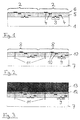
- the top metallization level 4 can also be from a passivation layer 6 made of, for example, silicon oxide and silicon nitride be covered.
- a second component substrate 7 likewise comprises a plurality of, usually identical, chips 8 arranged according to a defined scheme, which contain circuit structures 9, such as a MOS transistor, and one or more metallization levels 10.
- This substrate 7 is constructed essentially similarly to the first component substrate 1, but the circuit structures 9 are generally different in their function.
- the second component substrate has via holes 11 at the points at which the electrical contact to the underlying circuit structures of the first substrate is to be made later. The via holes 11 are so deep that they extend to below the layer with circuit structures 9 (FIG. 2).
- the passivation is opened at the top metallization level at certain measuring points.
- the individual chips of the substrate are then subjected to a functional test and the defective chips are identified (for example with an ink jet). A passivation layer is then applied again in order to protect the exposed measuring points again.
- An adhesive layer 12 is applied to the entire surface of the surface of the second substrate 7 made of an organic material, such as polyimide or photoresist.
- This adhesive layer 12 with a thickness of typically 1-2 ⁇ m can also cause a planarization of the surface.
- an auxiliary substrate 13 such as a silicon or quartz wafer, glued.
- the auxiliary substrate 13 is used as a handling substrate for the others Process steps use and protect the surface of the component substrate 7 during further processing. (Fig. 3).
- the second component substrate 7 by etching and / or grinding thinned from the back to the via holes 11 so that the thickness of the substrate 7 below the circuit structures 9 only a few Micrometer, typically 1-5 microns.
- the selected one depends Residual thickness also depends on the type of circuits contained.
- the second component substrate 7 with the handling substrate 13 is individual Chips cut. This can be done with an etching process, by sawing or with done with a laser. Then the marked, intact chips to the first component substrate 1 provided with an adhesive layer 14 applied side by side.
- the adhesive layer 14 typically has a thickness 1 - 2 ⁇ m can cause a planarization of the surface.
- the handling substrates 13 are e.g. by etching or Grind away and the exposed adhesive layer 12 typically with one Oxygen plasma or a solvent removed over the entire surface. After this Sticking the chips has trenches on the surface of the first substrate between the individual chips that have a very low aspect ratio have. Through a planarization step in which the layer 15 is deposited , these trenches are now filled in and a flat surface generated.
- the first component substrate 1 with the two component levels can now be used like a conventional silicon substrate with standard technology devices further process (Fig. 4).
- the electrical contact can of course be done in other ways can be realized, e.g. as soon as the chips are placed on the lower one Substrate using prepared front and rear contacts (see introduction to the description: Y. Hayashi et al.).
Description
Die Erfindung betrifft ein Verfahren zur Herstellung einer dreidimensionalen integrierten Schaltung. Unter dreidimensionaler Integration versteht man die vertikale Verbindung von Bauelementen, die mittels Planartechnik hergestellt wurden. Die Vorteile eines dreidimensional integrierten mikroelektronischen Systems sind u.a. die bei gleichen Designregeln erreichbaren höheren Packungsdichten und Schaltgeschwindigkeiten gegenüber zweidimensionalen Systemen. Letzteres ist zum einen bedingt durch kürzere Leitungswege zwischen den einzelnen Bauelementen oder Schaltungen, zum anderen durch die Möglichkeit der parallelen Informationsverarbeitung. Die Steigerung der Leistungsfähigkeit des Systems ist bei Realisierung einer Verbindungstechnik mit örtlich frei wählbaren höchstintegrierbaren vertikalen Kontakten optimal.The invention relates to a method for producing a three-dimensional integrated Circuit. Three-dimensional integration means that vertical connection of components made using planar technology were. The advantages of a three-dimensionally integrated microelectronic Systems include the higher achievable with the same design rules Packing densities and switching speeds compared to two-dimensional Systems. The latter is partly due to shorter cable routes between the individual components or circuits, on the other hand through the possibility of parallel information processing. The increase in performance of the system is included in the implementation of a connection technology optimally selectable, highly integrable vertical contacts.
Zur Herstellung dreidimensionaler Schaltungsanordnungen mit frei wählbaren vertikalen Kontakten sind folgende Verfahren bekannt:For the production of three-dimensional circuit arrangements with freely selectable The following methods are known for vertical contacts:
Y. Akasaka, Proc. IEEE 74 (1986) 1703, schlägt vor, auf eine fertig prozessierte Bauelementeschicht polykristallines Silizium abzuscheiden und zu rekristallisieren, so daß in der rekristallisierten Schicht weitere Bauelemente gefertigt werden können. Nachteile dieser Methode sind die ausbeutereduzierende Degradation der Bauelemente in der unteren Ebene durch die hohe thermische Belastung beim Rekristallisierungsprozeß, sowie die notwendigerweise serielle Prozessierung des Gesamtsystems. Letzteres bedingt zum einen entsprechend lange Durchlaufzeiten bei der Fertigung und hat zum anderen eine Ausbeuteminderung durch Aufsummierung der prozeßbedingten Ausfälle zur Folge. Beides erhöht die Fertigungskosten beträchtlich gegenüber einer Prozessierung der einzelnen Ebenen getrennt voneinander in verschiedenen Substraten.Y. Akasaka, Proc. IEEE 74 (1986) 1703, suggests a fully processed Deposition and recrystallization of component layer polycrystalline silicon, so that additional components are manufactured in the recrystallized layer can be. The disadvantages of this method are the yield-reducing degradation of the components in the lower level due to the high thermal Load in the recrystallization process, as well as the necessarily serial Processing of the overall system. The latter is conditional on the one hand long throughput times during production and secondly has a reduction in yield by adding up the process-related failures. Both increases the manufacturing costs considerably compared to processing of the individual levels separately from each other in different substrates.
Aus Y. Hayashi et al., Proc. 8th Int. Workshop on Future Electron Devices, 1990, p. 85, ist es bekannt, zunächst die einzelnen Bauelementeebenen getrennt voneinander in verschiedenen Substraten herzustellen. Anschließend werden die Substrate auf wenige Mikrometer gedünnt, mit Vorder- und Rückseitenkontakten versehen und mittels eines Bondverfahrens vertikal verbunden. Für die Bereitstellung der Vorder- und Rückseitenkontakte sind jedoch Sonderprozesse notwendig sind, die in der Standard - Halbleiterfertigung (CMOS) nicht vorgesehen sind, nämlich MOS - inkompatible Materialien (z.B. Gold) und Rückseitenstrukturierung des Substrates.From Y. Hayashi et al., Proc. 8th Int. Workshop on Future Electron Devices, 1990, p. 85, it is known to first separate the individual component levels from one another to manufacture in different substrates. Then the Substrates thinned to a few micrometers, with front and back contacts provided and vertically connected by means of a bonding process. For the provision the front and back contacts are special processes are necessary, which are not provided for in standard semiconductor manufacturing (CMOS) are, namely MOS - incompatible materials (e.g. gold) and back structuring of the substrate.
Die US 4,939,568 beschreibt ein Verfahren zur Herstellung einer dreidimensionalen integrierten Schaltungsstruktur durch Stapelung einzelner ICs zu einem Einzelchipstapel auf einem Trägersubstrat. Hierzu wird zunächst ein Substrat mit fertigprozessierten ICs in einzelne Chips unterteilt, womit die Prozessierung auf Waferebene beendet ist. Die Chips werden getestet, und ein erster einzelner Chip wird mittels Thermokompression auf ein Trägersubstrat aufgebracht. Nach diesem Schritt wird ein weiterer Chip in der gleichen Weise auf den ersten Chip aufgebracht. Es wird somit zunächst ein erster Chipstapel fertiggestellt, bevor mit der Herstellung eines weiteren Chipstapels auf einem anderen Trägersubstrat begonnen wird. Eine Weiterprozessierung der Chipstapel auf Waferebene ist mit diesem Verfahren daher nicht möglich. US 4,939,568 describes a method for producing a three-dimensional integrated circuit structure by stacking individual ICs into a single chip stack on a carrier substrate. For this purpose, a substrate is first used Completely processed ICs divided into individual chips, with the processing on Wafer level is finished. The chips are tested, and a first one Chip is applied to a carrier substrate by means of thermal compression. To This step will add another chip in the same way to the first chip upset. A first chip stack is thus completed before with the production of a further stack of chips on another carrier substrate is started. Further processing of the chip stack at the wafer level is therefore not possible with this method.
Aus der EP-A-0531723 ist ein Verfahren zur Herstellung dreidimensionaler Multichip-Stapel bekannt. Dabei werden vereinzelte Chips dergestalt mit einem geeigneten Träger verbunden, daß die Schutzoberfläche des Chips angrenzend an die obere Oberfläche des Trägers angeordnet ist. In einem folgenden Schritt wird die freiliegende zweite Oberfläche des Chips in einer geeigneten Ätzlösung geätzt. Anschließend werden weitere Schichten aufgebracht, und der Stapelprozeß wird dann wiederholt, indem Chips jeweils aufeinander hinzugefügt werden, wobei jeder seine aktive Schicht angrenzend an die zuletzt gedünnte freiliegende Oberfläche des Stapels positioniert hat. Dabei werden bei einer Vereinzelung der Chips jeweils nur die funktionsfähigen Chips ausgewählt. Alternativ kann auch eine wafermäßige Bearbeitung der Chips stattfinden, dabei findet jedoch keine Auswahl der funktionsfähigen Chips statt.EP-A-0531723 describes a method for producing three-dimensional multichip stacks known. Scattered chips are so made with a suitable carrier connected that the protective surface of the chip adjacent to the top surface the carrier is arranged. In a subsequent step, the exposed second Surface of the chip etched in a suitable etching solution. Then be additional layers are applied, and the stacking process is then repeated by Chips are added to each other, each with its active layer adjacent positioned on the last thinned exposed surface of the stack. When the chips are separated, only the functional chips are used selected. Alternatively, the chips can also be processed in the form of a wafer, however, there is no selection of the functional chips.
Darüber hinaus wird in International Electron Devices Meeting, 8. Dezember 1991, Seiten 25.6.1. bis 25.6.4.,Y. Hayashi et al. "A New Three-Dimensional IC Fabrication Technology, Stacking Thin Film Dual-CMOS Layers" eine neuartige dreidimensionale integrierte Schaltung beschrieben, bei dem Blöcke aus sogenanntem Dünnfilm DUAL-CMOS ICs miteinander verbunden werden. In diesen DUAL-CMOS ICs werden p-MOSFETs auf n-MOSFETs gestapelt, indem eine Laserstrahl-Tempertechnik verwendet wird. Durch mechanisch-chemisches Polieren werden die Substrate der integrierten Schaltungen gedünnt und dann miteinander verbunden. Darüber hinaus ist aus der deutschen Patentschrift Nr. 43 14 913 ein Verfahren zur Herstellung eines Bauelements mit einer Kontaktstrukturierung für vertikale Kontaktierung mit weiteren Halbleiterbauelementen bekannt. Das Halbleiterbauelement mit einer Kontaktstrukturierung für vertikale Kontaktierung mit weiteren Bauelementen weist ein Substrat auf, das auf einer Oberseite eine Schichtstruktur mit zu kontaktierenden Bereichen aufweist, bei dem mindestens ein Metallstift vorhanden ist, der dieses Substrat senkrecht zu der Schichtstruktur durchbohrt, bei dem das Substrat soweit gedünnt ist, daß der Metallstift die Unterseite des Substrats überragt und bei der gegebenenfalls auf der Oberseite Metallkontakte aus niedrigschmelzendem Metall vorhanden sind. In addition, at the International Electron Devices Meeting, December 8, 1991, Pages 25.6.1. to 25.6.4., Y. Hayashi et al. "A New Three-Dimensional IC Fabrication Technology, Stacking Thin Film Dual CMOS Layers "a novel three-dimensional Integrated circuit described, in which blocks made of so-called thin film DUAL-CMOS ICs are interconnected. In these DUAL-CMOS ICs are p-MOSFETs stacked on n-MOSFETs using a laser beam annealing technique becomes. The substrates are integrated by mechanical-chemical polishing Circuits thinned and then connected together. In addition, from the German Patent No. 43 14 913 a method for producing a component with a contact structuring for vertical contacting with other semiconductor components known. The semiconductor device with a contact structuring for vertical contacting with other components has a substrate that an upper side has a layer structure with areas to be contacted, at which at least one metal pin is present, this substrate perpendicular to the Drilled layer structure in which the substrate is thinned so far that the metal pin extends beyond the underside of the substrate and, if necessary, on the top Metal contacts made of low-melting metal are available.
Ein wesentlicher Nachteil der bisher genannten Verfahren ist dadurch bedingt, daß die in der Siliziumtechnologie zur Verfügung stehenden Geräte nur eine Bearbeitung (Prozessierung) von scheibenförmigen Substraten, den sog. Wafern, zulassen. Eine Prozessierung davon verschiedener Substrate, insbesondere von einzelnen Chips, ist nur in experimentellen Versuchsanlagen möglich, jedoch nicht im Rahmen einer industriellen Fertigung mit den geforderten hohen Ausbeuten.A major disadvantage of the previously mentioned methods is that that the devices available in silicon technology are only one machining (Processing) of disk-shaped substrates, the so-called wafers, allow. A processing of different substrates, especially of single chips, is only possible in experimental pilot plants, however not in the context of an industrial production with the required high Exploit.
Die US 4,954,875 beschreibt ein Verfahren zur dreidimensionalen Integration
durch Stapelung einzelner Wafer, bei dem die Verbindung der einzelnen
Bauelementeebenen über besonders geformte Vias hergestellt wird.
Beim Zusammenfügen von Substraten, die eine Vielzahl von identischen Bausteinen,
den sog. Chips, enthalten, ergibt sich die resultierende Ausbeute eines
mehrlagigen Systems aus dem Produkt der Einzelausbeuten. Dies führt dazu,
daß die Ausbeute eines mehrere Bauelementeebenen umfassenden Systems,
wie das der US 4,954,875 nach den bekannten Verfahren drastisch abnimmt. So
erhält man bei einer Ausbeute einer Einzelebene von 80 % bei einem Gesamtsystem
aus 10 Ebenen nur mehr eine resultierende Gesamtausbeute von etwa
10 %, womit ein derartiges System unwirtschaftlich wird und der Einsatz dieser
Technik auf wenige spezielle Einsatzfelder beschränkt wird. Die Ausbeute eines
Bauelementesubstrates hängt dabei auch von der Art der Schaltungen und des
verwendeten Herstellungsprozesses ab. So erzielt man z.B. in der Fertigung von
Speicherbausteinen sehr hohe Ausbeuten, während bei Logikbausteinen, wie
Mikroprozessoren, eine deutlich geringere Ausbeute erreicht wird. Insbesondere
wenn mehrere Arten solcher Schaltungen übereinandergestapelt werden, wird
damit die Gesamtausbeute überproportional durch die Schaltungsart mit der
geringsten Ausbeute bestimmt.No. 4,954,875 describes a method for three-dimensional integration by stacking individual wafers, in which the connection of the individual component levels is established via specially shaped vias.
When substrates that contain a large number of identical building blocks, the so-called chips, are joined together, the resultant yield of a multilayer system results from the product of the individual yields. As a result, the yield of a system comprising several component levels, such as that of US Pat. No. 4,954,875, drops drastically according to the known processes. With a yield of a single level of 80% for a total system of 10 levels, only a resulting overall yield of about 10% is obtained, which makes such a system uneconomical and the use of this technology is restricted to a few special fields of application. The yield of a component substrate also depends on the type of circuits and the manufacturing process used. For example, very high yields are achieved in the production of memory modules, while a significantly lower yield is achieved with logic modules such as microprocessors. In particular, if several types of such circuits are stacked on top of one another, the overall yield is determined disproportionately by the type of circuit with the lowest yield.
Der Erfindung liegt die Aufgabe zugrunde, ein Verfahren zur Herstellung einer dreidimensionalen integrierten Schaltung anzugeben, mit dem unter Verwendung der üblichen industriellen Standardausrüstung auf Waferebene eine deutliche Ausbeutesteigerung gegenüber bisher bekannten Verfahren erzielt wird.The invention has for its object a method for producing a to indicate three-dimensional integrated circuit with which using the usual industrial standard equipment at the wafer level Yield increase over previously known methods is achieved.
Diese Aufgabe wird erfindungsgemäß mit dem Verfahren nach Anspruch 1 gelöst.
Besondere Ausgestaltungen des Verfahrens sind Gegenstand der
Unteransprüche. This object is achieved with the method according to
In dem erfindungsgemäßen Verfahren werden zwei fertig prozessierte Substrate
(Wafer), die jeweils Schaltungsstrukturen und Metallisierungsebenen enthalten,
beispielsweise über eine Haftschicht miteinander verbunden. Die Haftschicht
kann hierbei zusätzlich eine passivierende Funktion ausüben (Anspruch 7)
und/oder eine Planarisierung der Oberfläche bewirken (Anspruch 8). Dabei wird
das obere Substrat (zweites Substrat) vorher einem Funktionstest unterzogen,
mit dem die intakten Chips des Substrates selektiert werden. Anschließend wird
dieses Substrat von der Rückseite her gedünnt und in einzelne Chips zerlegt.
Danach werden nur selektierte, intakte Chips auf das, mit einer Haftschicht
versehene, untere Substrat (erstes Substrat) nebeneinander justiert aufgebracht
und damit zu einer neuen Chipebene zusammengesetzt. Auf diese Weise wird
ein Wafer bereitgestellt, der in der neu aufgebrachten Chipebene nur intakte
Chips enthält.
Das untere Substrat kann hierbei auch bereits mehrere Bauelementelagen in
Form von Bauelementestapeln enthalten. Die Chips des oberen Substrates werden
entweder im Rahmen des Verfahrens dem Funktionstest unterzogen
(Anspruch 2) oder es wird ein bereits geprüftes Substrat mit getesteten und z.B.
markierten defekten Chips bereitgestellt und eingesetzt. Auf das obere Substrat
wird schließlich vor dem Dünnen und Zerteilen ein Hilfssubstrat aufgebracht.
Statt des Dünnens des oberen Substrates bis nahe an die Bauelementelagen
heran kann auch im Falle eines SOI-Substrates der Substratbereich unterhalb
der Oxidschicht entfernt werden.In the method according to the invention, two completely processed substrates (wafers), each containing circuit structures and metallization levels, are connected to one another, for example, via an adhesive layer. The adhesive layer can additionally have a passivating function (claim 7) and / or a planarization of the surface (claim 8). The upper substrate (second substrate) is previously subjected to a functional test with which the intact chips of the substrate are selected. This substrate is then thinned from the back and broken down into individual chips. Thereafter, only selected, intact chips are applied to the lower substrate (first substrate), which is provided with an adhesive layer, in an aligned manner and are thus assembled to form a new chip level. In this way, a wafer is provided which contains only intact chips in the newly applied chip level.
The lower substrate can already contain several component layers in the form of component stacks. The chips of the upper substrate are either subjected to the functional test as part of the method (claim 2) or an already tested substrate with tested and, for example, marked, defective chips is provided and used. Finally, an auxiliary substrate is applied to the upper substrate before thinning and dicing. Instead of thinning the upper substrate close to the component layers, the substrate area below the oxide layer can also be removed in the case of an SOI substrate.
Da auf dem unteren Substrat nun einzelne Chips aufgebracht worden sind, ist
keine zusammenhängende Oberfläche mehr vorhanden (Gräben zwischen den
Chips), so daß bestimmte Prozeßschritte, insbesondere Photolithographiemodule,
nicht mehr mit hoher Ausbeute durchgeführt werden können. Deshalb wird
nun vorzugsweise ein Planarisierungsschritt eingefügt (Anspruch 9).
Die Planarisierung kann mit verschiedenen Verfahren durchgeführt werden. Dabei
wird zuerst eine Isolationsschicht, wie z.B. Spin-on-Glas oder ein CVD - Oxid,
aufgebracht, um die Gräben aufzufüllen. Anschließend wird die Oberfläche eingeebnet,
was durch Rückätzen, mechanisches oder chemomechanisches
Schleifen erfolgt.
Weitere Prozesse, die nicht auf Chipebene realisierbar sind, können nach dem
Planarisierungsschritt problemlos an dem Substrat mit vorselektierten Chips
durchgeführt werden.Since individual chips have now been applied to the lower substrate, there is no longer any coherent surface (trenches between the chips), so that certain process steps, in particular photolithography modules, can no longer be carried out with a high yield. Therefore, a planarization step is now preferably inserted (claim 9).
The planarization can be carried out using various methods. An insulation layer, such as spin-on glass or a CVD oxide, is first applied to fill up the trenches. The surface is then leveled, which is done by etching back, mechanical or chemomechanical grinding.
After the planarization step, further processes that cannot be implemented at the chip level can be carried out without problems on the substrate with pre-selected chips.
Anschließend wird z.B. über Vialöcher (Anspruch 10), die bereits bei der Prozessierung der Einzelsubstrate in die Chips eingebracht wurden und nun bis zu einer Metallisierungsebene des unteren Substrates durchgeätzt werden, die elektrische Verbindung zwischen je einer Metallisierungsebene der oberen und der unteren Schaltungsebene hergestellt. Dabei wird die Photomaske zur Strukturierung auf jeden einzelnen Chip über Justierstrukturen separat justiert, um etwaige Maßabweichungen durch das Aufbringen der einzelnen Chips auszugleichen und eine hohe Justiergenauigkeit zu erreichen.Then e.g. Via holes (claim 10) already during processing of the individual substrates have been introduced into the chips and now up to are etched through a metallization level of the lower substrate, the electrical connection between one metallization level each of the upper and the lower circuit level. The photomask becomes Structuring on each individual chip is adjusted separately using adjustment structures, to compensate for any dimensional deviations caused by the application of the individual chips and to achieve high adjustment accuracy.
Danach kann das Substrat, das in der Bauelementeebene nur noch getestete und funktionsfähige Chips enthält, in gängigen Fertigungsanlagen weiter verarbeitet werden.Then the substrate can only be tested in the component level and contains functional chips, further processed in common manufacturing plants become.
In gleicher Weise kann nun auch eine weitere Bauelementeebene chipweise aufgebracht werden (Anspruch 3). Hierbei dient der bisher hergestellte Bauelementestapel mit zugehörigem Substrat als neues unteres Substrat. Dabei ist bei diesem Verfahren die Anzahl der Ebenen nicht beschränkt. Außerdem kann nicht nur eine Einzelebene, sondern auch ein bereits aus mehreren Ebenen bestehender Teilstapel chipweise aufgebracht werden.In the same way, a further component level can now also be used chip by chip be applied (claim 3). The previously manufactured component stack serves here with the associated substrate as the new lower substrate. It is this method does not limit the number of levels. Besides, can not just a single level, but also an already existing one Partial stacks are applied chip by chip.
Als Substrate sind monokristalline Siliziumsubstrate, SOI - Substrate oder Substrate verschiedener Technologiefamilien, wie z.B. III - V - Halbleiter geeignet. Monocrystalline silicon substrates, SOI substrates or Substrates from different technology families, e.g. III - V semiconductors suitable.
Insgesamt werden bei diesem Verfahren nur bekannte und eingeführte Verfahrensschritte
verwendet, so daß keine neuen Prozesse entwickelt werden müssen.
Mit dem erfindungsgemäßen Verfahren werden nur intakte Chips jeweils auf die
darunterliegenden Bauelementelagen aufgebracht. Damit wird in vorteilhafter
Weise die Abhängigkeit der Ausbeute des Gesamtsystems von der Ausbeute
der einzelnen prozessierten Substrate stark verringert. Es können jeweils nur
einzelne defekte Chips einer Bauelementelage ausgesondert werden, so daß
nicht mehr ganze Bauelementestapel aufgrund einer einzigen defekten Lage unbrauchbar
werden. Durch das erfindungsgemäße Verfahren werden somit die
Ausbeute bei der Herstellung dreidimensionaler integrierter Schaltungen deutlich
gesteigert und die Herstellungskosten gesenkt.Overall, only known and introduced process steps are used in this process, so that no new processes have to be developed.
With the method according to the invention, only intact chips are applied to the underlying component layers. The dependence of the yield of the overall system on the yield of the individual processed substrates is thus greatly reduced. Only individual defective chips of a component layer can be separated out, so that entire component stacks are no longer unusable due to a single defective layer. The method according to the invention thus significantly increases the yield in the production of three-dimensional integrated circuits and reduces the production costs.
Im folgenden wird die Erfindung anhand der Zeichnungen und eines Ausführungsbeispiels näher erläutert.In the following the invention with reference to the drawings and an embodiment explained in more detail.
Dabei zeigen:
- Fig. 1
- ein erstes Bauelementesubstrat mit Schaltungsstrukturen und Metallisierungsebenen (unteres Substrat),
- Fig. 2
- ein zweites Bauelementesubstrat mit Schaltungsstrukturen, Metallisierungsebenen und Vialöchern (oberes Substrat),
- Fig. 3
- das zweite Bauelementesubstrat mit Haftschicht und Hilfssubstrat,
- Fig. 4
- das erste Bauelementesubstrat mit einer chipweise aufgebrachten zweiten Bauelementeebene nach Planarisierung der Oberfläche, und
- Fig. 5
- zwei vertikal verbundene Bauelementeebenen.
- Fig. 1
- a first component substrate with circuit structures and metallization levels (lower substrate),
- Fig. 2
- a second component substrate with circuit structures, metallization levels and via holes (upper substrate),
- Fig. 3
- the second component substrate with adhesive layer and auxiliary substrate,
- Fig. 4
- the first component substrate with a second component level applied chip by chip after planarization of the surface, and
- Fig. 5
- two vertically connected component levels.
Ein erstes Bauelementesubstrat 1 aus z.B. monokristallinem Silizium umfaßt
mehrere, nach einem definierten Schema angeordnete, üblicherweise identische
Chips 2, die Schaltungsstrukturen 3, wie beispielsweise einen MOS - Transistor,
und eine oder mehrere Metallisierungsebenen 4 enthalten, die typischerweise
aus Aluminum, einer Aluminiumlegierung oder anderen Materalien, wie Kupfer
oder Wolfram, bestehen und zur elektrischen Isolation von einer Oxidschicht 5,
die zu Planarisierungszwecken auch mit Bor und / oder Phosphor dotiert sein
kann, umgeben sind. Die oberste Metallisierungsebene 4 kann dabei auch von
einer Passivierungsschicht 6 aus beispielsweise Siliziumoxid und Siliziumnitrid
bedeckt sein. Weiterhin sind Justagestrukturen zum genauen Zusammenfügen
mehrerer Ebenen implementiert (in Fig. 1 nicht gezeigt). Unterhalb der
Schaltungsstrukturen 3 weist das Substrat eine Dicke von z.B. 625 µm auf.
Dieses Bauelementesubstrat stellt das untere Substrat des mehrlagigen
Systems dar (Fig. 1).A
Ein zweites Bauelementesubstrat 7 umfaßt ebenfalls mehrere, nach einem
definierten Schema angeordnete, üblicherweise identische Chips 8, die Schaltungsstrukturen
9, wie beispielsweise einen MOS - Transistor, und eine oder
mehrere Metallisierungsebenen 10 enthalten. Dieses Substrat 7 ist im wesentlichen
ähnlich aufgebaut wie das erste Bauelementesubstrat 1, die Schaltungsstrukturen
9 sind aber in der Regel von ihrer Funktion her unterschiedlich.
Desweiteren weist das zweite Bauelementesubstrat Vialöcher 11 an den Stellen
auf, an denen später die elektrische Kontaktierung zu darunterliegenden
Schaltungsstrukturen des ersten Substrates erfolgen soll. Die Vialöcher 11 sind
so tief, daß sie bis unterhalb der Schicht mit Schaltungsstrukturen 9 reichen (Fig.
2).
Nach Fertigstellung des Bauelementesubstrates 7 wird die Passivierung auf der
obersten Metallisierungsebene an bestimmten Meßstellen geöffnet. Danach
werden die einzelnen Chips des Substrates einem Funktionstest unterzogen und
die defekten Chips gekennzeichnet (z.B. mit einem Tintenstrahl). Anschließend
wird erneut eine Passivierungsschicht aufgebracht, um die offenliegenden
Meßstellen wieder zu schützen. A
After completion of the
Auf die Oberfläche des zweiten Substrates 7 wird ganzflächig eine Haftschicht 12
aus einem organischen Material, wie Polyimid oder Photolack, aufgebracht.
Diese Haftschicht 12 mit einer Dicke von typischerweise 1 - 2 µm kann außerdem
eine Planarisierung der Oberfläche bewirken. Auf die Haftschicht 12 wird
schließlich ein Hilfssubstrat 13, wie beispielsweise ein Silizium- oder Quarzwafer,
geklebt. Das Hilfssubstrat 13 wird als Handlingsubstrat für die weiteren
Prozeßschritte verwendet und schützt die Oberfläche des Bauelementesubstrates
7 bei der weiteren Bearbeitung. (Fig. 3).An adhesive layer 12 is applied to the entire surface of the surface of the
Danach wird das zweite Bauelementesubstrat 7 durch Ätzen und/oder Schleifen
von der Rückseite her bis an die Vialöcher 11 heran gedünnt, so daß die Dicke
des Substrates 7 unterhalb der Schaltungsstrukturen 9 nur noch wenige
Mikrometer, typischerweise 1 - 5 µm, beträgt. Dabei hängt die gewählte
Restdicke auch von der Art der enthaltenen Schaltungen ab.Thereafter, the
Nun wird das zweite Bauelementesubstrat 7 mit dem Handlingsubstrat 13 in einzelne
Chips zerteilt. Dies kann dabei mit einem Ätzprozeß, durch Sägen oder mit
einem Laser erfolgen. Daraufhin werden die gekennzeichneten, intakten Chips
auf das, mit einer Haftschicht 14 versehene, erste Bauelementesubstrat 1 justiert
nebeneinander aufgebracht. Die Haftschicht 14 mit einer Dicke von typischerweise
1 - 2 µm kann dabei eine Planarisierung der Oberfläche bewirken.
Anschließend werden die Handlingsubstrate 13 z.B. durch Abätzen oder
Abschleifen entfernt und die freiliegende Haftschicht 12 typischerweise mit einem
Sauerstoffplasma oder einem Lösungsmittel ganzflächig entfernt. Nach dem
Aufkleben der Chips weist die Oberfläche des ersten Substrates nun Gräben
zwischen den einzelnen Chips auf, die ein sehr niedriges Aspektverhältnis
besitzen. Durch einen Planarisierungsschritt, in dem die Schicht 15 abgeschieden
wird, werden diese Gräben nun aufgefüllt und eine ebene Oberfläche
erzeugt. Das erste Bauelementesubstrat 1 mit den beiden Bauelementeebenen
läßt sich nun wie ein übliches Siliziumsubstrat mit Standard - Technologiegeräten
weiterverarbeiten (Fig. 4). Now the
Danach wird schließlich die vertikale Verbindung 16 zwischen einer Metallisierungsebene
10 der oberen Bauelementeebene (Substrat 7) und einer Metallisierungsebene
4 der unteren Bauelementeebene (Substrat 1) hergestellt. Dazu
werden mit einem Photolithographieschritt ein Kontaktloch zu einer Metallisierungsebene
10 der oberen Bauelementeebene und die vorbereiteten Vialöcher
11 bis zu einer Metallisierungsebene 4 der unteren Bauelementeebene geöffnet
und durch Metallabscheidung und Strukturierung eine elektrische Verbindung
realisiert. Schließlich wird auf die Oberfläche noch eine Passivierungsschicht 17
abgeschieden (Fig. 5).Then finally the
Die elektrische Kontaktierung kann selbstverständlich auch auf andere Weise realisiert werden, so z.B. bereits beim Aufbringen der Chips auf das untere Substrat mittels vorbereiteter Vorder- und Rückseitenkontakte (vgl. Beschreibungseinleitung: Y. Hayashi et al.).The electrical contact can of course be done in other ways can be realized, e.g. as soon as the chips are placed on the lower one Substrate using prepared front and rear contacts (see introduction to the description: Y. Hayashi et al.).
Claims (12)
- Method of manufacturing a three-dimensional
integrated circuit having the following method steps:providing a first substrate (1) which contains on a first side one or more ready-processed component levels (3), which have beside one another a large number of independent components or circuits, components or circuits of a plurality of component levels forming component stacks;providing a second substrate (7) which contains on a second side one or more ready-processed component levels (9) which have beside one another a large number of independent components or circuits, components or circuits of a plurality of component levels forming component stacks, and the components, component stacks or circuits being tested for their ability to function in order to distinguish functioning from non-functioning components, component stacks or circuits;connecting the second substrate (7) to an auxiliary substrate (13) on the second side;thinning or removing the second substrate (7) on the side facing the second side;dividing the auxiliary substrate (13) with the connected component levels into individual chips which respectively contain functioning or nor-functioning components, component stacks or circuits;justified application of the chips which contain functioning components, component stacks or circuits, beside one another to the first substrate (1) on the first side;removing the auxiliary substrate (13);producing the electrical contacts between the components, component stacks or circuits of the applied chips and the components, component stacks or circuits of the first substrate, it being possible for this method step to take place already during the application of the chips. - Method according to claim 1,
characterised in that
the provision of the second substrate comprises the following method steps:providing a second substrate (7) which contains on a second side one or more ready-processed component levels (9), which have beside one another a large number of independent components or circuits, components or circuits of a plurality of component levels forming component stacks, andfunction test of the individual components, component stacks or circuits of the second substrate to distinguish functioning from non-functioning components, component stacks or circuits. - Method according to claim 1 or 2,
characterised in that
in order to construct a three-dimensional integrated circuit having more than two component levels, the method is carried out several times in succession, the processed first substrate of the respectively preceding process being used as the first substrate each time the process is repeated. - Method according to one of claims 1 to 3,
characterised in that
the first and second substrates respectively contain exactly one component level. - Method according to one of claims 1 to 4,
characterised in that
the auxiliary substrate (13) is connected to the second substrate (7) via an adhesive layer (12). - Method according to one of claims 1 to 5,
characterised in that
the chips are applied by means of an adhesive layer (14) to the first side of the first substrate (1). - Method according to claim 5 or 6,
characterised in that
an adhesive layer with passivating properties is used. - Method according to one of claims 5 to 7,
characterised in that
an adhesive layer is used which causes planarisation of the surface. - Method according to one of claims 1 to 8,
characterised in that
the trenches which occur between the individual chips after the justified application of same, are planarised. - Method according to one of claims 1 to 9,
characterised in that
the electrical contacts between the components, component stacks or circuits of the applied chips and the components, component stacks or circuits of the first substrate are produced through contact holes and/or via-holes (11). - Method according to one of claims 1 to 10,
characterised in that
the second substrate (7) is thinned by means of etching and/or polishing. - Method according to one of claims 1 to 11,
characterised in that
an SOI substrate is used as the second substrate (7).
Applications Claiming Priority (2)
| Application Number | Priority Date | Filing Date | Title |
|---|---|---|---|
| DE4433845 | 1994-09-22 | ||
| DE4433845A DE4433845A1 (en) | 1994-09-22 | 1994-09-22 | Method of manufacturing a three-dimensional integrated circuit |
Publications (2)
| Publication Number | Publication Date |
|---|---|
| EP0703618A1 EP0703618A1 (en) | 1996-03-27 |
| EP0703618B1 true EP0703618B1 (en) | 2001-06-06 |
Family
ID=6528903
Family Applications (1)
| Application Number | Title | Priority Date | Filing Date |
|---|---|---|---|
| EP95113423A Expired - Lifetime EP0703618B1 (en) | 1994-09-22 | 1995-08-26 | Method for fabricating a three dimensional integrated circuit |
Country Status (4)
| Country | Link |
|---|---|
| US (1) | US5563084A (en) |
| EP (1) | EP0703618B1 (en) |
| JP (1) | JP3986575B2 (en) |
| DE (2) | DE4433845A1 (en) |
Cited By (3)
| Publication number | Priority date | Publication date | Assignee | Title |
|---|---|---|---|---|
| US7705466B2 (en) | 1997-04-04 | 2010-04-27 | Elm Technology Corporation | Three dimensional multi layer memory and control logic integrated circuit structure |
| US8080442B2 (en) | 2002-08-08 | 2011-12-20 | Elm Technology Corporation | Vertical system integration |
| US10028742B2 (en) | 2005-11-09 | 2018-07-24 | Ethicon Llc | Staple cartridge comprising staples with different unformed heights |
Families Citing this family (320)
| Publication number | Priority date | Publication date | Assignee | Title |
|---|---|---|---|---|
| US5354695A (en) | 1992-04-08 | 1994-10-11 | Leedy Glenn J | Membrane dielectric isolation IC fabrication |
| US5665649A (en) * | 1993-05-21 | 1997-09-09 | Gardiner Communications Corporation | Process for forming a semiconductor device base array and mounting semiconductor devices thereon |
| DE4433846C2 (en) * | 1994-09-22 | 1999-06-02 | Fraunhofer Ges Forschung | Method of making a vertical integrated circuit structure |
| DE19516487C1 (en) * | 1995-05-05 | 1996-07-25 | Fraunhofer Ges Forschung | Vertical integration process for microelectronic system |
| DE19543540C1 (en) | 1995-11-22 | 1996-11-21 | Siemens Ag | Vertically integrated semiconductor component |
| US5851845A (en) * | 1995-12-18 | 1998-12-22 | Micron Technology, Inc. | Process for packaging a semiconductor die using dicing and testing |
| US5817530A (en) * | 1996-05-20 | 1998-10-06 | Micron Technology, Inc. | Use of conductive lines on the back side of wafers and dice for semiconductor interconnects |
| US8018058B2 (en) * | 2004-06-21 | 2011-09-13 | Besang Inc. | Semiconductor memory device |
| KR100904771B1 (en) | 2003-06-24 | 2009-06-26 | 이상윤 | 3-Dimensional Integrated Circuit Structure and Method of Making the Same |
| US7888764B2 (en) * | 2003-06-24 | 2011-02-15 | Sang-Yun Lee | Three-dimensional integrated circuit structure |
| US20050280155A1 (en) * | 2004-06-21 | 2005-12-22 | Sang-Yun Lee | Semiconductor bonding and layer transfer method |
| US8058142B2 (en) * | 1996-11-04 | 2011-11-15 | Besang Inc. | Bonded semiconductor structure and method of making the same |
| US5915167A (en) * | 1997-04-04 | 1999-06-22 | Elm Technology Corporation | Three dimensional structure memory |
| WO1999016131A1 (en) * | 1997-09-19 | 1999-04-01 | Fraunhofer-Gesellschaft zur Förderung der angewandten Forschung e.V. | Method for wiring semi-conductor components in order to prevent product piracy and manipulation, semi-conductor component made according to this method and use of said semi-conductor component in a chip card |
| DE19746641B4 (en) * | 1997-09-19 | 2006-02-23 | Fraunhofer-Gesellschaft zur Förderung der angewandten Forschung e.V. | Wiring method for semiconductor devices for preventing product piracy and product manipulation and use of the semiconductor device in a smart card |
| DE19746642C2 (en) * | 1997-10-22 | 2002-07-18 | Fraunhofer Ges Forschung | Method for producing a semiconductor component and its use in a chip card |
| DE19748666C2 (en) * | 1997-11-04 | 2002-08-29 | Fraunhofer Ges Forschung | Wiring method for microelectronic systems for preventing product piracy and product manipulation, microelectronic system produced by the method and use of the microelectronic system in a chip card |
| DE19750316A1 (en) * | 1997-11-13 | 1999-05-27 | Siemens Ag | Silicon foil carrier manufacturing method for chip card |
| US6275297B1 (en) | 1998-08-19 | 2001-08-14 | Sc Technology | Method of measuring depths of structures on a semiconductor substrate |
| DE19838439C1 (en) * | 1998-08-24 | 2000-04-27 | Fraunhofer Ges Forschung | Vertically integrated thin film photodiode, for photodetector used e.g. in optical data storage and transmission, is produced by thinning and reflective coating of a photodiode substrate bonded to a temporary substrate |
| EP1116180B1 (en) | 1998-09-03 | 2002-10-02 | Fraunhofer-Gesellschaft Zur Förderung Der Angewandten Forschung E.V. | Method for contacting a circuit chip |
| DE19849586C1 (en) * | 1998-10-27 | 2000-05-11 | Fraunhofer Ges Forschung | Three-dimensional IC production comprises opening of filled trenches before cutting a three-dimensional circuit structure into individual circuits |
| DE19853703A1 (en) | 1998-11-20 | 2000-05-25 | Giesecke & Devrient Gmbh | Chip production, especially for a chip card, comprises applying metallization onto a thinned finished chip wafer, bonded to a handling wafer, for connection by vias to the chip metallization and/or circuit structure |
| DE19856573C1 (en) | 1998-12-08 | 2000-05-18 | Fraunhofer Ges Forschung | Vertical integration of active circuit planes involves connecting two substrates so connection surfaces are electrically connected, reducing second substrate, freeing external connection surfaces |
| DE19918671B4 (en) * | 1999-04-23 | 2006-03-02 | Giesecke & Devrient Gmbh | Vertically integrable circuit and method for its manufacture |
| EP1171912B1 (en) | 1999-05-27 | 2003-09-24 | Fraunhofer-Gesellschaft zur Förderung der angewandten Forschung e.V. | Method for the vertical integration of electric components by reverse side contacting |
| DE19924935C1 (en) * | 1999-05-31 | 2000-11-30 | Fraunhofer Ges Forschung | Process for the production of three-dimensional circuits |
| US7582490B2 (en) | 1999-06-22 | 2009-09-01 | President And Fellows Of Harvard College | Controlled fabrication of gaps in electrically conducting structures |
| US6783643B2 (en) | 1999-06-22 | 2004-08-31 | President And Fellows Of Harvard College | Control of solid state dimensional features |
| AU5763000A (en) * | 1999-06-22 | 2001-01-09 | President And Fellows Of Harvard College | Molecular and atomic scale evaluation of biopolymers |
| US7118657B2 (en) | 1999-06-22 | 2006-10-10 | President And Fellows Of Harvard College | Pulsed ion beam control of solid state features |
| US7258838B2 (en) | 1999-06-22 | 2007-08-21 | President And Fellows Of Harvard College | Solid state molecular probe device |
| US6464842B1 (en) | 1999-06-22 | 2002-10-15 | President And Fellows Of Harvard College | Control of solid state dimensional features |
| US6650426B1 (en) | 1999-07-12 | 2003-11-18 | Sc Technology, Inc. | Endpoint determination for recess etching to a precise depth |
| DE19933472A1 (en) * | 1999-07-20 | 2001-02-01 | Daimler Chrysler Ag | Arrangement with network for signal processing, especially image data processing, has chips with network structures on bearer substrate networked via electrical connections in substrate |
| US6500694B1 (en) * | 2000-03-22 | 2002-12-31 | Ziptronix, Inc. | Three dimensional device integration method and integrated device |
| US6984571B1 (en) * | 1999-10-01 | 2006-01-10 | Ziptronix, Inc. | Three dimensional device integration method and integrated device |
| US6902987B1 (en) | 2000-02-16 | 2005-06-07 | Ziptronix, Inc. | Method for low temperature bonding and bonded structure |
| DE10008386A1 (en) * | 2000-02-23 | 2001-08-30 | Giesecke & Devrient Gmbh | Method for connecting substrates of a vertical, integrated circuit structure partitions a top substrate into a first subpart with a metallizing structure and a second silicon subpart with a circuit structure. |
| US6563133B1 (en) | 2000-08-09 | 2003-05-13 | Ziptronix, Inc. | Method of epitaxial-like wafer bonding at low temperature and bonded structure |
| US6674161B1 (en) * | 2000-10-03 | 2004-01-06 | Rambus Inc. | Semiconductor stacked die devices |
| EP1195808B1 (en) | 2000-10-04 | 2007-08-15 | Infineon Technologies AG | Method of fabricating a thin, free-standing semiconductor device layer and of making a three-dimensionally integrated circuit |
| EP1215721B1 (en) * | 2000-12-13 | 2008-01-23 | Infineon Technologies AG | Process for multistep processing of a thin and brittle Wafer |
| US6748994B2 (en) | 2001-04-11 | 2004-06-15 | Avery Dennison Corporation | Label applicator, method and label therefor |
| KR100394808B1 (en) * | 2001-07-19 | 2003-08-14 | 삼성전자주식회사 | Wafer level stack chip package and method for manufacturing the same |
| DE10164800B4 (en) | 2001-11-02 | 2005-03-31 | Infineon Technologies Ag | Method for producing an electronic component with a plurality of chips stacked on top of one another and contacted with one another |
| DE10153609C2 (en) * | 2001-11-02 | 2003-10-16 | Infineon Technologies Ag | Method for producing an electronic component with a plurality of chips stacked on top of one another and contacted with one another |
| DE10200399B4 (en) * | 2002-01-08 | 2008-03-27 | Advanced Micro Devices, Inc., Sunnyvale | A method for producing a three-dimensionally integrated semiconductor device and a three-dimensionally integrated semiconductor device |
| EP1367645A3 (en) * | 2002-05-31 | 2006-12-27 | Fujitsu Limited | Semiconductor device and manufacturing method thereof |
| TWI234253B (en) * | 2002-05-31 | 2005-06-11 | Fujitsu Ltd | Semiconductor device and manufacturing method thereof |
| US7064055B2 (en) * | 2002-12-31 | 2006-06-20 | Massachusetts Institute Of Technology | Method of forming a multi-layer semiconductor structure having a seamless bonding interface |
| WO2004061961A1 (en) * | 2002-12-31 | 2004-07-22 | Massachusetts Institute Of Technology | Multi-layer integrated semiconductor structure having an electrical shielding portion |
| US20100133695A1 (en) * | 2003-01-12 | 2010-06-03 | Sang-Yun Lee | Electronic circuit with embedded memory |
| US6770495B1 (en) * | 2003-01-15 | 2004-08-03 | Advanced Micro Devices, Inc. | Method for revealing active regions in a SOI structure for DUT backside inspection |
| US6962835B2 (en) | 2003-02-07 | 2005-11-08 | Ziptronix, Inc. | Method for room temperature metal direct bonding |
| US7109092B2 (en) | 2003-05-19 | 2006-09-19 | Ziptronix, Inc. | Method of room temperature covalent bonding |
| DE10323394B4 (en) * | 2003-05-20 | 2006-09-28 | Fraunhofer-Gesellschaft zur Förderung der angewandten Forschung e.V. | Method for producing an electrical contact between two semiconductor pieces and method for producing an arrangement of semiconductor pieces |
| JP4819320B2 (en) * | 2003-05-28 | 2011-11-24 | 株式会社オクテック | Manufacturing method of semiconductor device |
| US8071438B2 (en) * | 2003-06-24 | 2011-12-06 | Besang Inc. | Semiconductor circuit |
| US20100190334A1 (en) * | 2003-06-24 | 2010-07-29 | Sang-Yun Lee | Three-dimensional semiconductor structure and method of manufacturing the same |
| DE10342980B3 (en) * | 2003-09-17 | 2005-01-05 | Disco Hi-Tec Europe Gmbh | Semiconductor chip stack formation method for manufacture of 3D-packages with function testing of chips for removal or unacceptable chips and replacement by acceptable chips |
| JP2005123463A (en) | 2003-10-17 | 2005-05-12 | Seiko Epson Corp | Semiconductor device, its manufacturing method, semiconductor device module, circuit board, and electronic equipment |
| JP4307284B2 (en) | 2004-02-17 | 2009-08-05 | 三洋電機株式会社 | Manufacturing method of semiconductor device |
| JP5354765B2 (en) * | 2004-08-20 | 2013-11-27 | カミヤチョウ アイピー ホールディングス | Manufacturing method of semiconductor device having three-dimensional laminated structure |
| DE102004056970B4 (en) * | 2004-11-25 | 2008-07-03 | Fraunhofer-Gesellschaft zur Förderung der angewandten Forschung e.V. | Method and device for generating an electrical contact between two semiconductor pieces by a mechanical element |
| US8392021B2 (en) | 2005-02-18 | 2013-03-05 | Irobot Corporation | Autonomous surface cleaning robot for wet cleaning |
| US20110143506A1 (en) * | 2009-12-10 | 2011-06-16 | Sang-Yun Lee | Method for fabricating a semiconductor memory device |
| US8367524B2 (en) * | 2005-03-29 | 2013-02-05 | Sang-Yun Lee | Three-dimensional integrated circuit structure |
| US20110001172A1 (en) * | 2005-03-29 | 2011-01-06 | Sang-Yun Lee | Three-dimensional integrated circuit structure |
| US7462552B2 (en) * | 2005-05-23 | 2008-12-09 | Ziptronix, Inc. | Method of detachable direct bonding at low temperatures |
| US8456015B2 (en) | 2005-06-14 | 2013-06-04 | Cufer Asset Ltd. L.L.C. | Triaxial through-chip connection |
| US7534722B2 (en) | 2005-06-14 | 2009-05-19 | John Trezza | Back-to-front via process |
| US7851348B2 (en) | 2005-06-14 | 2010-12-14 | Abhay Misra | Routingless chip architecture |
| US7838997B2 (en) | 2005-06-14 | 2010-11-23 | John Trezza | Remote chip attachment |
| US7560813B2 (en) | 2005-06-14 | 2009-07-14 | John Trezza | Chip-based thermo-stack |
| US7969015B2 (en) | 2005-06-14 | 2011-06-28 | Cufer Asset Ltd. L.L.C. | Inverse chip connector |
| US7521806B2 (en) * | 2005-06-14 | 2009-04-21 | John Trezza | Chip spanning connection |
| US7687400B2 (en) | 2005-06-14 | 2010-03-30 | John Trezza | Side stacking apparatus and method |
| US7786592B2 (en) * | 2005-06-14 | 2010-08-31 | John Trezza | Chip capacitive coupling |
| US7767493B2 (en) | 2005-06-14 | 2010-08-03 | John Trezza | Post & penetration interconnection |
| US7781886B2 (en) | 2005-06-14 | 2010-08-24 | John Trezza | Electronic chip contact structure |
| US7776715B2 (en) * | 2005-07-26 | 2010-08-17 | Micron Technology, Inc. | Reverse construction memory cell |
| US7622313B2 (en) * | 2005-07-29 | 2009-11-24 | Freescale Semiconductor, Inc. | Fabrication of three dimensional integrated circuit employing multiple die panels |
| US7485968B2 (en) * | 2005-08-11 | 2009-02-03 | Ziptronix, Inc. | 3D IC method and device |
| US7378339B2 (en) * | 2006-03-30 | 2008-05-27 | Freescale Semiconductor, Inc. | Barrier for use in 3-D integration of circuits |
| US7687397B2 (en) | 2006-06-06 | 2010-03-30 | John Trezza | Front-end processed wafer having through-chip connections |
| US8513789B2 (en) * | 2006-10-10 | 2013-08-20 | Tessera, Inc. | Edge connect wafer level stacking with leads extending along edges |
| US7901989B2 (en) * | 2006-10-10 | 2011-03-08 | Tessera, Inc. | Reconstituted wafer level stacking |
| US7829438B2 (en) * | 2006-10-10 | 2010-11-09 | Tessera, Inc. | Edge connect wafer level stacking |
| KR101175393B1 (en) * | 2006-10-17 | 2012-08-20 | 쿠퍼 에셋 엘티디. 엘.엘.씨. | wafer via formation |
| US7952195B2 (en) * | 2006-12-28 | 2011-05-31 | Tessera, Inc. | Stacked packages with bridging traces |
| US7705613B2 (en) * | 2007-01-03 | 2010-04-27 | Abhay Misra | Sensitivity capacitive sensor |
| US7670874B2 (en) | 2007-02-16 | 2010-03-02 | John Trezza | Plated pillar package formation |
| US7850060B2 (en) * | 2007-04-05 | 2010-12-14 | John Trezza | Heat cycle-able connection |
| US7748116B2 (en) * | 2007-04-05 | 2010-07-06 | John Trezza | Mobile binding in an electronic connection |
| US7960210B2 (en) * | 2007-04-23 | 2011-06-14 | Cufer Asset Ltd. L.L.C. | Ultra-thin chip packaging |
| US8367471B2 (en) | 2007-06-15 | 2013-02-05 | Micron Technology, Inc. | Semiconductor assemblies, stacked semiconductor devices, and methods of manufacturing semiconductor assemblies and stacked semiconductor devices |
| US8461672B2 (en) * | 2007-07-27 | 2013-06-11 | Tessera, Inc. | Reconstituted wafer stack packaging with after-applied pad extensions |
| US8193092B2 (en) | 2007-07-31 | 2012-06-05 | Micron Technology, Inc. | Semiconductor devices including a through-substrate conductive member with an exposed end and methods of manufacturing such semiconductor devices |
| KR101533663B1 (en) | 2007-08-03 | 2015-07-03 | 테세라, 인코포레이티드 | Stack packages using reconstituted wafers |
| US8043895B2 (en) | 2007-08-09 | 2011-10-25 | Tessera, Inc. | Method of fabricating stacked assembly including plurality of stacked microelectronic elements |
| CN102067310B (en) * | 2008-06-16 | 2013-08-21 | 泰塞拉公司 | Stacking of wafer-level chip scale packages having edge contacts and manufacture method thereof |
| CN102422412A (en) * | 2009-03-13 | 2012-04-18 | 德塞拉股份有限公司 | Stacked microelectronic assemblies having vias extending through bond pads |
| US8669778B1 (en) | 2009-04-14 | 2014-03-11 | Monolithic 3D Inc. | Method for design and manufacturing of a 3D semiconductor device |
| US8754533B2 (en) | 2009-04-14 | 2014-06-17 | Monolithic 3D Inc. | Monolithic three-dimensional semiconductor device and structure |
| US9711407B2 (en) | 2009-04-14 | 2017-07-18 | Monolithic 3D Inc. | Method of manufacturing a three dimensional integrated circuit by transfer of a mono-crystalline layer |
| US8384426B2 (en) | 2009-04-14 | 2013-02-26 | Monolithic 3D Inc. | Semiconductor device and structure |
| US8373439B2 (en) | 2009-04-14 | 2013-02-12 | Monolithic 3D Inc. | 3D semiconductor device |
| US8427200B2 (en) | 2009-04-14 | 2013-04-23 | Monolithic 3D Inc. | 3D semiconductor device |
| US8405420B2 (en) | 2009-04-14 | 2013-03-26 | Monolithic 3D Inc. | System comprising a semiconductor device and structure |
| US9577642B2 (en) | 2009-04-14 | 2017-02-21 | Monolithic 3D Inc. | Method to form a 3D semiconductor device |
| US7986042B2 (en) | 2009-04-14 | 2011-07-26 | Monolithic 3D Inc. | Method for fabrication of a semiconductor device and structure |
| US8395191B2 (en) | 2009-10-12 | 2013-03-12 | Monolithic 3D Inc. | Semiconductor device and structure |
| US9509313B2 (en) | 2009-04-14 | 2016-11-29 | Monolithic 3D Inc. | 3D semiconductor device |
| US8362482B2 (en) | 2009-04-14 | 2013-01-29 | Monolithic 3D Inc. | Semiconductor device and structure |
| US8378715B2 (en) | 2009-04-14 | 2013-02-19 | Monolithic 3D Inc. | Method to construct systems |
| US8058137B1 (en) | 2009-04-14 | 2011-11-15 | Monolithic 3D Inc. | Method for fabrication of a semiconductor device and structure |
| US8362800B2 (en) | 2010-10-13 | 2013-01-29 | Monolithic 3D Inc. | 3D semiconductor device including field repairable logics |
| US8536023B2 (en) | 2010-11-22 | 2013-09-17 | Monolithic 3D Inc. | Method of manufacturing a semiconductor device and structure |
| US11018133B2 (en) | 2009-10-12 | 2021-05-25 | Monolithic 3D Inc. | 3D integrated circuit |
| US10354995B2 (en) | 2009-10-12 | 2019-07-16 | Monolithic 3D Inc. | Semiconductor memory device and structure |
| US10910364B2 (en) | 2009-10-12 | 2021-02-02 | Monolitaic 3D Inc. | 3D semiconductor device |
| US10043781B2 (en) | 2009-10-12 | 2018-08-07 | Monolithic 3D Inc. | 3D semiconductor device and structure |
| US8476145B2 (en) | 2010-10-13 | 2013-07-02 | Monolithic 3D Inc. | Method of fabricating a semiconductor device and structure |
| US10366970B2 (en) | 2009-10-12 | 2019-07-30 | Monolithic 3D Inc. | 3D semiconductor device and structure |
| US8581349B1 (en) | 2011-05-02 | 2013-11-12 | Monolithic 3D Inc. | 3D memory semiconductor device and structure |
| US10157909B2 (en) | 2009-10-12 | 2018-12-18 | Monolithic 3D Inc. | 3D semiconductor device and structure |
| US11374118B2 (en) | 2009-10-12 | 2022-06-28 | Monolithic 3D Inc. | Method to form a 3D integrated circuit |
| US8294159B2 (en) | 2009-10-12 | 2012-10-23 | Monolithic 3D Inc. | Method for fabrication of a semiconductor device and structure |
| US9099424B1 (en) | 2012-08-10 | 2015-08-04 | Monolithic 3D Inc. | Semiconductor system, device and structure with heat removal |
| US8742476B1 (en) | 2012-11-27 | 2014-06-03 | Monolithic 3D Inc. | Semiconductor device and structure |
| US8450804B2 (en) | 2011-03-06 | 2013-05-28 | Monolithic 3D Inc. | Semiconductor device and structure for heat removal |
| US10388863B2 (en) | 2009-10-12 | 2019-08-20 | Monolithic 3D Inc. | 3D memory device and structure |
| US8841777B2 (en) * | 2010-01-12 | 2014-09-23 | International Business Machines Corporation | Bonded structure employing metal semiconductor alloy bonding |
| US8492886B2 (en) | 2010-02-16 | 2013-07-23 | Monolithic 3D Inc | 3D integrated circuit with logic |
| US8026521B1 (en) | 2010-10-11 | 2011-09-27 | Monolithic 3D Inc. | Semiconductor device and structure |
| US8373230B1 (en) | 2010-10-13 | 2013-02-12 | Monolithic 3D Inc. | Method for fabrication of a semiconductor device and structure |
| US8461035B1 (en) | 2010-09-30 | 2013-06-11 | Monolithic 3D Inc. | Method for fabrication of a semiconductor device and structure |
| US8541819B1 (en) | 2010-12-09 | 2013-09-24 | Monolithic 3D Inc. | Semiconductor device and structure |
| US9099526B2 (en) | 2010-02-16 | 2015-08-04 | Monolithic 3D Inc. | Integrated circuit device and structure |
| US8288795B2 (en) | 2010-03-02 | 2012-10-16 | Micron Technology, Inc. | Thyristor based memory cells, devices and systems including the same and methods for forming the same |
| US9608119B2 (en) | 2010-03-02 | 2017-03-28 | Micron Technology, Inc. | Semiconductor-metal-on-insulator structures, methods of forming such structures, and semiconductor devices including such structures |
| US8513722B2 (en) | 2010-03-02 | 2013-08-20 | Micron Technology, Inc. | Floating body cell structures, devices including same, and methods for forming same |
| US9646869B2 (en) * | 2010-03-02 | 2017-05-09 | Micron Technology, Inc. | Semiconductor devices including a diode structure over a conductive strap and methods of forming such semiconductor devices |
| US8507966B2 (en) | 2010-03-02 | 2013-08-13 | Micron Technology, Inc. | Semiconductor cells, arrays, devices and systems having a buried conductive line and methods for forming the same |
| US8525342B2 (en) * | 2010-04-12 | 2013-09-03 | Qualcomm Incorporated | Dual-side interconnected CMOS for stacked integrated circuits |
| KR101134819B1 (en) | 2010-07-02 | 2012-04-13 | 이상윤 | Method for fabricating semiconductor memory |
| US9219005B2 (en) | 2011-06-28 | 2015-12-22 | Monolithic 3D Inc. | Semiconductor system and device |
| US9953925B2 (en) | 2011-06-28 | 2018-04-24 | Monolithic 3D Inc. | Semiconductor system and device |
| US10217667B2 (en) | 2011-06-28 | 2019-02-26 | Monolithic 3D Inc. | 3D semiconductor device, fabrication method and system |
| US8642416B2 (en) | 2010-07-30 | 2014-02-04 | Monolithic 3D Inc. | Method of forming three dimensional integrated circuit devices using layer transfer technique |
| US8901613B2 (en) | 2011-03-06 | 2014-12-02 | Monolithic 3D Inc. | Semiconductor device and structure for heat removal |
| US8163581B1 (en) | 2010-10-13 | 2012-04-24 | Monolith IC 3D | Semiconductor and optoelectronic devices |
| US8273610B2 (en) | 2010-11-18 | 2012-09-25 | Monolithic 3D Inc. | Method of constructing a semiconductor device and structure |
| US10497713B2 (en) | 2010-11-18 | 2019-12-03 | Monolithic 3D Inc. | 3D semiconductor memory device and structure |
| US11482440B2 (en) | 2010-12-16 | 2022-10-25 | Monolithic 3D Inc. | 3D semiconductor device and structure with a built-in test circuit for repairing faulty circuits |
| US10290682B2 (en) | 2010-10-11 | 2019-05-14 | Monolithic 3D Inc. | 3D IC semiconductor device and structure with stacked memory |
| US8114757B1 (en) | 2010-10-11 | 2012-02-14 | Monolithic 3D Inc. | Semiconductor device and structure |
| US11469271B2 (en) | 2010-10-11 | 2022-10-11 | Monolithic 3D Inc. | Method to produce 3D semiconductor devices and structures with memory |
| US11227897B2 (en) | 2010-10-11 | 2022-01-18 | Monolithic 3D Inc. | Method for producing a 3D semiconductor memory device and structure |
| US11257867B1 (en) | 2010-10-11 | 2022-02-22 | Monolithic 3D Inc. | 3D semiconductor device and structure with oxide bonds |
| US11315980B1 (en) | 2010-10-11 | 2022-04-26 | Monolithic 3D Inc. | 3D semiconductor device and structure with transistors |
| US11018191B1 (en) | 2010-10-11 | 2021-05-25 | Monolithic 3D Inc. | 3D semiconductor device and structure |
| US11158674B2 (en) | 2010-10-11 | 2021-10-26 | Monolithic 3D Inc. | Method to produce a 3D semiconductor device and structure |
| US10896931B1 (en) | 2010-10-11 | 2021-01-19 | Monolithic 3D Inc. | 3D semiconductor device and structure |
| US11024673B1 (en) | 2010-10-11 | 2021-06-01 | Monolithic 3D Inc. | 3D semiconductor device and structure |
| US11600667B1 (en) | 2010-10-11 | 2023-03-07 | Monolithic 3D Inc. | Method to produce 3D semiconductor devices and structures with memory |
| US10833108B2 (en) | 2010-10-13 | 2020-11-10 | Monolithic 3D Inc. | 3D microdisplay device and structure |
| US11855100B2 (en) | 2010-10-13 | 2023-12-26 | Monolithic 3D Inc. | Multilevel semiconductor device and structure with oxide bonding |
| US11855114B2 (en) | 2010-10-13 | 2023-12-26 | Monolithic 3D Inc. | Multilevel semiconductor device and structure with image sensors and wafer bonding |
| US11929372B2 (en) | 2010-10-13 | 2024-03-12 | Monolithic 3D Inc. | Multilevel semiconductor device and structure with image sensors and wafer bonding |
| US10943934B2 (en) | 2010-10-13 | 2021-03-09 | Monolithic 3D Inc. | Multilevel semiconductor device and structure |
| US10998374B1 (en) | 2010-10-13 | 2021-05-04 | Monolithic 3D Inc. | Multilevel semiconductor device and structure |
| US10978501B1 (en) | 2010-10-13 | 2021-04-13 | Monolithic 3D Inc. | Multilevel semiconductor device and structure with waveguides |
| US11869915B2 (en) | 2010-10-13 | 2024-01-09 | Monolithic 3D Inc. | Multilevel semiconductor device and structure with image sensors and wafer bonding |
| US11163112B2 (en) | 2010-10-13 | 2021-11-02 | Monolithic 3D Inc. | Multilevel semiconductor device and structure with electromagnetic modulators |
| US11437368B2 (en) | 2010-10-13 | 2022-09-06 | Monolithic 3D Inc. | Multilevel semiconductor device and structure with oxide bonding |
| US11327227B2 (en) | 2010-10-13 | 2022-05-10 | Monolithic 3D Inc. | Multilevel semiconductor device and structure with electromagnetic modulators |
| US9197804B1 (en) | 2011-10-14 | 2015-11-24 | Monolithic 3D Inc. | Semiconductor and optoelectronic devices |
| US8379458B1 (en) | 2010-10-13 | 2013-02-19 | Monolithic 3D Inc. | Semiconductor device and structure |
| US11063071B1 (en) | 2010-10-13 | 2021-07-13 | Monolithic 3D Inc. | Multilevel semiconductor device and structure with waveguides |
| US11404466B2 (en) | 2010-10-13 | 2022-08-02 | Monolithic 3D Inc. | Multilevel semiconductor device and structure with image sensors |
| US11605663B2 (en) | 2010-10-13 | 2023-03-14 | Monolithic 3D Inc. | Multilevel semiconductor device and structure with image sensors and wafer bonding |
| US11694922B2 (en) | 2010-10-13 | 2023-07-04 | Monolithic 3D Inc. | Multilevel semiconductor device and structure with oxide bonding |
| US11133344B2 (en) | 2010-10-13 | 2021-09-28 | Monolithic 3D Inc. | Multilevel semiconductor device and structure with image sensors |
| US11164898B2 (en) | 2010-10-13 | 2021-11-02 | Monolithic 3D Inc. | Multilevel semiconductor device and structure |
| US10679977B2 (en) | 2010-10-13 | 2020-06-09 | Monolithic 3D Inc. | 3D microdisplay device and structure |
| US11043523B1 (en) | 2010-10-13 | 2021-06-22 | Monolithic 3D Inc. | Multilevel semiconductor device and structure with image sensors |
| US9064881B2 (en) * | 2010-11-11 | 2015-06-23 | Taiwan Semiconductor Manufacturing Company, Ltd. | Protecting flip-chip package using pre-applied fillet |
| US11121021B2 (en) | 2010-11-18 | 2021-09-14 | Monolithic 3D Inc. | 3D semiconductor device and structure |
| US11862503B2 (en) | 2010-11-18 | 2024-01-02 | Monolithic 3D Inc. | Method for producing a 3D semiconductor device and structure with memory cells and multiple metal layers |
| US11482438B2 (en) | 2010-11-18 | 2022-10-25 | Monolithic 3D Inc. | Methods for producing a 3D semiconductor memory device and structure |
| US11164770B1 (en) | 2010-11-18 | 2021-11-02 | Monolithic 3D Inc. | Method for producing a 3D semiconductor memory device and structure |
| US11443971B2 (en) | 2010-11-18 | 2022-09-13 | Monolithic 3D Inc. | 3D semiconductor device and structure with memory |
| US11610802B2 (en) | 2010-11-18 | 2023-03-21 | Monolithic 3D Inc. | Method for producing a 3D semiconductor device and structure with single crystal transistors and metal gate electrodes |
| US11355380B2 (en) | 2010-11-18 | 2022-06-07 | Monolithic 3D Inc. | Methods for producing 3D semiconductor memory device and structure utilizing alignment marks |
| US11018042B1 (en) | 2010-11-18 | 2021-05-25 | Monolithic 3D Inc. | 3D semiconductor memory device and structure |
| US11804396B2 (en) | 2010-11-18 | 2023-10-31 | Monolithic 3D Inc. | Methods for producing a 3D semiconductor device and structure with memory cells and multiple metal layers |
| US11569117B2 (en) | 2010-11-18 | 2023-01-31 | Monolithic 3D Inc. | 3D semiconductor device and structure with single-crystal layers |
| US11615977B2 (en) | 2010-11-18 | 2023-03-28 | Monolithic 3D Inc. | 3D semiconductor memory device and structure |
| US11784082B2 (en) | 2010-11-18 | 2023-10-10 | Monolithic 3D Inc. | 3D semiconductor device and structure with bonding |
| US11482439B2 (en) | 2010-11-18 | 2022-10-25 | Monolithic 3D Inc. | Methods for producing a 3D semiconductor memory device comprising charge trap junction-less transistors |
| US11735462B2 (en) | 2010-11-18 | 2023-08-22 | Monolithic 3D Inc. | 3D semiconductor device and structure with single-crystal layers |
| US11508605B2 (en) | 2010-11-18 | 2022-11-22 | Monolithic 3D Inc. | 3D semiconductor memory device and structure |
| US11107721B2 (en) | 2010-11-18 | 2021-08-31 | Monolithic 3D Inc. | 3D semiconductor device and structure with NAND logic |
| US11854857B1 (en) | 2010-11-18 | 2023-12-26 | Monolithic 3D Inc. | Methods for producing a 3D semiconductor device and structure with memory cells and multiple metal layers |
| US11004719B1 (en) | 2010-11-18 | 2021-05-11 | Monolithic 3D Inc. | Methods for producing a 3D semiconductor memory device and structure |
| US11211279B2 (en) | 2010-11-18 | 2021-12-28 | Monolithic 3D Inc. | Method for processing a 3D integrated circuit and structure |
| US11094576B1 (en) | 2010-11-18 | 2021-08-17 | Monolithic 3D Inc. | Methods for producing a 3D semiconductor memory device and structure |
| US11355381B2 (en) | 2010-11-18 | 2022-06-07 | Monolithic 3D Inc. | 3D semiconductor memory device and structure |
| US11031275B2 (en) | 2010-11-18 | 2021-06-08 | Monolithic 3D Inc. | 3D semiconductor device and structure with memory |
| US11521888B2 (en) | 2010-11-18 | 2022-12-06 | Monolithic 3D Inc. | 3D semiconductor device and structure with high-k metal gate transistors |
| US11495484B2 (en) | 2010-11-18 | 2022-11-08 | Monolithic 3D Inc. | 3D semiconductor devices and structures with at least two single-crystal layers |
| US11923230B1 (en) | 2010-11-18 | 2024-03-05 | Monolithic 3D Inc. | 3D semiconductor device and structure with bonding |
| US11901210B2 (en) | 2010-11-18 | 2024-02-13 | Monolithic 3D Inc. | 3D semiconductor device and structure with memory |
| US8598621B2 (en) | 2011-02-11 | 2013-12-03 | Micron Technology, Inc. | Memory cells, memory arrays, methods of forming memory cells, and methods of forming a shared doped semiconductor region of a vertically oriented thyristor and a vertically oriented access transistor |
| US8952418B2 (en) | 2011-03-01 | 2015-02-10 | Micron Technology, Inc. | Gated bipolar junction transistors |
| US8975670B2 (en) | 2011-03-06 | 2015-03-10 | Monolithic 3D Inc. | Semiconductor device and structure for heat removal |
| US8519431B2 (en) | 2011-03-08 | 2013-08-27 | Micron Technology, Inc. | Thyristors |
| CN103503122B (en) | 2011-05-24 | 2016-05-18 | 索尼公司 | Semiconductor device |
| US10388568B2 (en) | 2011-06-28 | 2019-08-20 | Monolithic 3D Inc. | 3D semiconductor device and system |
| US8772848B2 (en) | 2011-07-26 | 2014-07-08 | Micron Technology, Inc. | Circuit structures, memory circuitry, and methods |
| US8687399B2 (en) | 2011-10-02 | 2014-04-01 | Monolithic 3D Inc. | Semiconductor device and structure |
| US9029173B2 (en) | 2011-10-18 | 2015-05-12 | Monolithic 3D Inc. | Method for fabrication of a semiconductor device and structure |
| DE102012200258A1 (en) | 2012-01-10 | 2013-07-11 | Fraunhofer-Gesellschaft zur Förderung der angewandten Forschung e.V. | Method for manufacturing three-dimension integrated chip, involves connecting contact surfaces of isolated components with integrated circuit portions of substrate, and removing another substrate from isolated components |
| US9000557B2 (en) | 2012-03-17 | 2015-04-07 | Zvi Or-Bach | Semiconductor device and structure |
| US11735501B1 (en) | 2012-04-09 | 2023-08-22 | Monolithic 3D Inc. | 3D semiconductor device and structure with metal layers and a connective path |
| US9954080B2 (en) * | 2012-04-09 | 2018-04-24 | Monolithic 3D Inc. | 3D integrated circuit device |
| US11410912B2 (en) | 2012-04-09 | 2022-08-09 | Monolithic 3D Inc. | 3D semiconductor device with vias and isolation layers |
| US8557632B1 (en) * | 2012-04-09 | 2013-10-15 | Monolithic 3D Inc. | Method for fabrication of a semiconductor device and structure |
| US11164811B2 (en) | 2012-04-09 | 2021-11-02 | Monolithic 3D Inc. | 3D semiconductor device with isolation layers and oxide-to-oxide bonding |
| US11088050B2 (en) | 2012-04-09 | 2021-08-10 | Monolithic 3D Inc. | 3D semiconductor device with isolation layers |
| US11616004B1 (en) | 2012-04-09 | 2023-03-28 | Monolithic 3D Inc. | 3D semiconductor device and structure with metal layers and a connective path |
| US9691869B2 (en) * | 2012-04-09 | 2017-06-27 | Monolithic 3D Inc. | Semiconductor devices and structures |
| US10038073B1 (en) * | 2012-04-09 | 2018-07-31 | Monolithic 3D Inc. | 3D integrated circuit device |
| US11476181B1 (en) | 2012-04-09 | 2022-10-18 | Monolithic 3D Inc. | 3D semiconductor device and structure with metal layers |
| US10600888B2 (en) | 2012-04-09 | 2020-03-24 | Monolithic 3D Inc. | 3D semiconductor device |
| US11694944B1 (en) | 2012-04-09 | 2023-07-04 | Monolithic 3D Inc. | 3D semiconductor device and structure with metal layers and a connective path |
| US11881443B2 (en) | 2012-04-09 | 2024-01-23 | Monolithic 3D Inc. | 3D semiconductor device and structure with metal layers and a connective path |
| US11594473B2 (en) | 2012-04-09 | 2023-02-28 | Monolithic 3D Inc. | 3D semiconductor device and structure with metal layers and a connective path |
| US8686428B1 (en) | 2012-11-16 | 2014-04-01 | Monolithic 3D Inc. | Semiconductor device and structure |
| US8574929B1 (en) | 2012-11-16 | 2013-11-05 | Monolithic 3D Inc. | Method to form a 3D semiconductor device and structure |
| US11309292B2 (en) | 2012-12-22 | 2022-04-19 | Monolithic 3D Inc. | 3D semiconductor device and structure with metal layers |
| US11916045B2 (en) | 2012-12-22 | 2024-02-27 | Monolithic 3D Inc. | 3D semiconductor device and structure with metal layers |
| US11967583B2 (en) | 2012-12-22 | 2024-04-23 | Monolithic 3D Inc. | 3D semiconductor device and structure with metal layers |
| US8674470B1 (en) | 2012-12-22 | 2014-03-18 | Monolithic 3D Inc. | Semiconductor device and structure |
| US11961827B1 (en) | 2012-12-22 | 2024-04-16 | Monolithic 3D Inc. | 3D semiconductor device and structure with metal layers |
| US11784169B2 (en) | 2012-12-22 | 2023-10-10 | Monolithic 3D Inc. | 3D semiconductor device and structure with metal layers |
| US11018116B2 (en) | 2012-12-22 | 2021-05-25 | Monolithic 3D Inc. | Method to form a 3D semiconductor device and structure |
| US11063024B1 (en) | 2012-12-22 | 2021-07-13 | Monlithic 3D Inc. | Method to form a 3D semiconductor device and structure |
| US11217565B2 (en) | 2012-12-22 | 2022-01-04 | Monolithic 3D Inc. | Method to form a 3D semiconductor device and structure |
| US10903089B1 (en) | 2012-12-29 | 2021-01-26 | Monolithic 3D Inc. | 3D semiconductor device and structure |
| US11004694B1 (en) | 2012-12-29 | 2021-05-11 | Monolithic 3D Inc. | 3D semiconductor device and structure |
| US10600657B2 (en) | 2012-12-29 | 2020-03-24 | Monolithic 3D Inc | 3D semiconductor device and structure |
| US11430667B2 (en) | 2012-12-29 | 2022-08-30 | Monolithic 3D Inc. | 3D semiconductor device and structure with bonding |
| US11430668B2 (en) | 2012-12-29 | 2022-08-30 | Monolithic 3D Inc. | 3D semiconductor device and structure with bonding |
| US10651054B2 (en) | 2012-12-29 | 2020-05-12 | Monolithic 3D Inc. | 3D semiconductor device and structure |
| US9871034B1 (en) | 2012-12-29 | 2018-01-16 | Monolithic 3D Inc. | Semiconductor device and structure |
| US11177140B2 (en) | 2012-12-29 | 2021-11-16 | Monolithic 3D Inc. | 3D semiconductor device and structure |
| US10115663B2 (en) | 2012-12-29 | 2018-10-30 | Monolithic 3D Inc. | 3D semiconductor device and structure |
| US11087995B1 (en) | 2012-12-29 | 2021-08-10 | Monolithic 3D Inc. | 3D semiconductor device and structure |
| US10892169B2 (en) | 2012-12-29 | 2021-01-12 | Monolithic 3D Inc. | 3D semiconductor device and structure |
| US9385058B1 (en) | 2012-12-29 | 2016-07-05 | Monolithic 3D Inc. | Semiconductor device and structure |
| US10325651B2 (en) | 2013-03-11 | 2019-06-18 | Monolithic 3D Inc. | 3D semiconductor device with stacked memory |
| US8902663B1 (en) | 2013-03-11 | 2014-12-02 | Monolithic 3D Inc. | Method of maintaining a memory state |
| US11869965B2 (en) | 2013-03-11 | 2024-01-09 | Monolithic 3D Inc. | 3D semiconductor device and structure with metal layers and memory cells |
| US11935949B1 (en) | 2013-03-11 | 2024-03-19 | Monolithic 3D Inc. | 3D semiconductor device and structure with metal layers and memory cells |
| US11398569B2 (en) | 2013-03-12 | 2022-07-26 | Monolithic 3D Inc. | 3D semiconductor device and structure |
| US11923374B2 (en) | 2013-03-12 | 2024-03-05 | Monolithic 3D Inc. | 3D semiconductor device and structure with metal layers |
| US8994404B1 (en) | 2013-03-12 | 2015-03-31 | Monolithic 3D Inc. | Semiconductor device and structure |
| US10840239B2 (en) | 2014-08-26 | 2020-11-17 | Monolithic 3D Inc. | 3D semiconductor device and structure |
| US11088130B2 (en) | 2014-01-28 | 2021-08-10 | Monolithic 3D Inc. | 3D semiconductor device and structure |
| US9117749B1 (en) | 2013-03-15 | 2015-08-25 | Monolithic 3D Inc. | Semiconductor device and structure |
| US10224279B2 (en) | 2013-03-15 | 2019-03-05 | Monolithic 3D Inc. | Semiconductor device and structure |
| US9021414B1 (en) | 2013-04-15 | 2015-04-28 | Monolithic 3D Inc. | Automation for monolithic 3D devices |
| US11487928B2 (en) | 2013-04-15 | 2022-11-01 | Monolithic 3D Inc. | Automation for monolithic 3D devices |
| US11574109B1 (en) | 2013-04-15 | 2023-02-07 | Monolithic 3D Inc | Automation methods for 3D integrated circuits and devices |
| US11270055B1 (en) | 2013-04-15 | 2022-03-08 | Monolithic 3D Inc. | Automation for monolithic 3D devices |
| US11341309B1 (en) | 2013-04-15 | 2022-05-24 | Monolithic 3D Inc. | Automation for monolithic 3D devices |
| US11720736B2 (en) | 2013-04-15 | 2023-08-08 | Monolithic 3D Inc. | Automation methods for 3D integrated circuits and devices |
| US11030371B2 (en) | 2013-04-15 | 2021-06-08 | Monolithic 3D Inc. | Automation for monolithic 3D devices |
| US11031394B1 (en) | 2014-01-28 | 2021-06-08 | Monolithic 3D Inc. | 3D semiconductor device and structure |
| US11107808B1 (en) | 2014-01-28 | 2021-08-31 | Monolithic 3D Inc. | 3D semiconductor device and structure |
| US10297586B2 (en) | 2015-03-09 | 2019-05-21 | Monolithic 3D Inc. | Methods for processing a 3D semiconductor device |
| US11011507B1 (en) | 2015-04-19 | 2021-05-18 | Monolithic 3D Inc. | 3D semiconductor device and structure |
| US11056468B1 (en) | 2015-04-19 | 2021-07-06 | Monolithic 3D Inc. | 3D semiconductor device and structure |
| US10381328B2 (en) | 2015-04-19 | 2019-08-13 | Monolithic 3D Inc. | Semiconductor device and structure |
| US10825779B2 (en) | 2015-04-19 | 2020-11-03 | Monolithic 3D Inc. | 3D semiconductor device and structure |
| US11956952B2 (en) | 2015-08-23 | 2024-04-09 | Monolithic 3D Inc. | Semiconductor memory device and structure |
| US9953941B2 (en) | 2015-08-25 | 2018-04-24 | Invensas Bonding Technologies, Inc. | Conductive barrier direct hybrid bonding |
| WO2017053329A1 (en) | 2015-09-21 | 2017-03-30 | Monolithic 3D Inc | 3d semiconductor device and structure |
| US10522225B1 (en) | 2015-10-02 | 2019-12-31 | Monolithic 3D Inc. | Semiconductor device with non-volatile memory |
| US11114464B2 (en) | 2015-10-24 | 2021-09-07 | Monolithic 3D Inc. | 3D semiconductor device and structure |
| US10418369B2 (en) | 2015-10-24 | 2019-09-17 | Monolithic 3D Inc. | Multi-level semiconductor memory device and structure |
| US11296115B1 (en) | 2015-10-24 | 2022-04-05 | Monolithic 3D Inc. | 3D semiconductor device and structure |
| US10847540B2 (en) | 2015-10-24 | 2020-11-24 | Monolithic 3D Inc. | 3D semiconductor memory device and structure |
| US11937422B2 (en) | 2015-11-07 | 2024-03-19 | Monolithic 3D Inc. | Semiconductor memory device and structure |
| US11114427B2 (en) | 2015-11-07 | 2021-09-07 | Monolithic 3D Inc. | 3D semiconductor processor and memory device and structure |
| US9852988B2 (en) | 2015-12-18 | 2017-12-26 | Invensas Bonding Technologies, Inc. | Increased contact alignment tolerance for direct bonding |
| US9748106B2 (en) * | 2016-01-21 | 2017-08-29 | Micron Technology, Inc. | Method for fabricating semiconductor package |
| RU2656030C2 (en) * | 2016-07-14 | 2018-05-30 | Акционерное общество "Концерн радиостроения "Вега" | Method of manufacturing three-dimensional electronic module |
| US11711928B2 (en) | 2016-10-10 | 2023-07-25 | Monolithic 3D Inc. | 3D memory devices and structures with control circuits |
| US11869591B2 (en) | 2016-10-10 | 2024-01-09 | Monolithic 3D Inc. | 3D memory devices and structures with control circuits |
| US11251149B2 (en) | 2016-10-10 | 2022-02-15 | Monolithic 3D Inc. | 3D memory device and structure |
| US11329059B1 (en) | 2016-10-10 | 2022-05-10 | Monolithic 3D Inc. | 3D memory devices and structures with thinned single crystal substrates |
| US11812620B2 (en) | 2016-10-10 | 2023-11-07 | Monolithic 3D Inc. | 3D DRAM memory devices and structures with control circuits |
| US11930648B1 (en) | 2016-10-10 | 2024-03-12 | Monolithic 3D Inc. | 3D memory devices and structures with metal layers |
| US10331839B2 (en) | 2017-08-18 | 2019-06-25 | Honeywell Federal Manufacturing & Technologies, Llc | System and method for obfuscation of electronic circuits |
| US10840205B2 (en) | 2017-09-24 | 2020-11-17 | Invensas Bonding Technologies, Inc. | Chemical mechanical polishing for hybrid bonding |
| US11056348B2 (en) | 2018-04-05 | 2021-07-06 | Invensas Bonding Technologies, Inc. | Bonding surfaces for microelectronics |
| US11393779B2 (en) | 2018-06-13 | 2022-07-19 | Invensas Bonding Technologies, Inc. | Large metal pads over TSV |
| KR20210009426A (en) | 2018-06-13 | 2021-01-26 | 인벤사스 본딩 테크놀로지스 인코포레이티드 | TV as a pad |
| US11011494B2 (en) | 2018-08-31 | 2021-05-18 | Invensas Bonding Technologies, Inc. | Layer structures for making direct metal-to-metal bonds at low temperatures in microelectronics |
| US11158573B2 (en) | 2018-10-22 | 2021-10-26 | Invensas Bonding Technologies, Inc. | Interconnect structures |
| US11158652B1 (en) | 2019-04-08 | 2021-10-26 | Monolithic 3D Inc. | 3D memory semiconductor devices and structures |
| US10892016B1 (en) | 2019-04-08 | 2021-01-12 | Monolithic 3D Inc. | 3D memory semiconductor devices and structures |
| US11018156B2 (en) | 2019-04-08 | 2021-05-25 | Monolithic 3D Inc. | 3D memory semiconductor devices and structures |
| US11763864B2 (en) | 2019-04-08 | 2023-09-19 | Monolithic 3D Inc. | 3D memory semiconductor devices and structures with bit-line pillars |
| US11296106B2 (en) | 2019-04-08 | 2022-04-05 | Monolithic 3D Inc. | 3D memory semiconductor devices and structures |
| US11264357B1 (en) | 2020-10-20 | 2022-03-01 | Invensas Corporation | Mixed exposure for large die |
Family Cites Families (16)
| Publication number | Priority date | Publication date | Assignee | Title |
|---|---|---|---|---|
| KR900008647B1 (en) * | 1986-03-20 | 1990-11-26 | 후지쓰 가부시끼가이샤 | A method for manufacturing three demensional i.c. |
| US4954875A (en) * | 1986-07-17 | 1990-09-04 | Laser Dynamics, Inc. | Semiconductor wafer array with electrically conductive compliant material |
| US4924589A (en) * | 1988-05-16 | 1990-05-15 | Leedy Glenn J | Method of making and testing an integrated circuit |
| US5104820A (en) * | 1989-07-07 | 1992-04-14 | Irvine Sensors Corporation | Method of fabricating electronic circuitry unit containing stacked IC layers having lead rerouting |
| JPH0344067A (en) * | 1989-07-11 | 1991-02-25 | Nec Corp | Laminating method of semiconductor substrate |
| JP2617798B2 (en) * | 1989-09-22 | 1997-06-04 | 三菱電機株式会社 | Stacked semiconductor device and method of manufacturing the same |
| US5208178A (en) * | 1990-08-02 | 1993-05-04 | Hitachi, Ltd. | Manufacturing a semiconductor integrated circuit device having on chip logic correction |
| US5202754A (en) * | 1991-09-13 | 1993-04-13 | International Business Machines Corporation | Three-dimensional multichip packages and methods of fabrication |
| US5270261A (en) * | 1991-09-13 | 1993-12-14 | International Business Machines Corporation | Three dimensional multichip package methods of fabrication |
| US5244818A (en) * | 1992-04-08 | 1993-09-14 | Georgia Tech Research Corporation | Processes for lift-off of thin film materials and for the fabrication of three dimensional integrated circuits |
| US5258318A (en) * | 1992-05-15 | 1993-11-02 | International Business Machines Corporation | Method of forming a BiCMOS SOI wafer having thin and thick SOI regions of silicon |
| US5489554A (en) * | 1992-07-21 | 1996-02-06 | Hughes Aircraft Company | Method of making a 3-dimensional circuit assembly having electrical contacts that extend through the IC layer |
| US5324687A (en) * | 1992-10-16 | 1994-06-28 | General Electric Company | Method for thinning of integrated circuit chips for lightweight packaged electronic systems |
| DE4314913C1 (en) * | 1993-05-05 | 1994-08-25 | Siemens Ag | Method for producing a semiconductor component having a contact structure for vertical contact-making with other semiconductor components |
| US5391257A (en) * | 1993-12-10 | 1995-02-21 | Rockwell International Corporation | Method of transferring a thin film to an alternate substrate |
| GB9401770D0 (en) * | 1994-01-31 | 1994-03-23 | Philips Electronics Uk Ltd | Manufacture of electronic devices comprising thin-film circuits |
-
1994
- 1994-09-22 DE DE4433845A patent/DE4433845A1/en not_active Withdrawn
-
1995
- 1995-08-26 EP EP95113423A patent/EP0703618B1/en not_active Expired - Lifetime
- 1995-08-26 DE DE59509316T patent/DE59509316D1/en not_active Expired - Lifetime
- 1995-09-22 US US08/532,858 patent/US5563084A/en not_active Expired - Lifetime
- 1995-09-22 JP JP24473295A patent/JP3986575B2/en not_active Expired - Lifetime
Cited By (15)
| Publication number | Priority date | Publication date | Assignee | Title |
|---|---|---|---|---|
| US8841778B2 (en) | 1997-04-04 | 2014-09-23 | Glenn J Leedy | Three dimensional memory structure |
| US8824159B2 (en) | 1997-04-04 | 2014-09-02 | Glenn J. Leedy | Three dimensional structure memory |
| US9401183B2 (en) | 1997-04-04 | 2016-07-26 | Glenn J. Leedy | Stacked integrated memory device |
| US8288206B2 (en) | 1997-04-04 | 2012-10-16 | Elm Technology Corp | Three dimensional structure memory |
| US8318538B2 (en) | 1997-04-04 | 2012-11-27 | Elm Technology Corp. | Three dimensional structure memory |
| US8410617B2 (en) | 1997-04-04 | 2013-04-02 | Elm Technology | Three dimensional structure memory |
| US8933570B2 (en) | 1997-04-04 | 2015-01-13 | Elm Technology Corp. | Three dimensional structure memory |
| US8629542B2 (en) | 1997-04-04 | 2014-01-14 | Glenn J. Leedy | Three dimensional structure memory |
| US8928119B2 (en) | 1997-04-04 | 2015-01-06 | Glenn J. Leedy | Three dimensional structure memory |
| US7705466B2 (en) | 1997-04-04 | 2010-04-27 | Elm Technology Corporation | Three dimensional multi layer memory and control logic integrated circuit structure |
| US8907499B2 (en) | 1997-04-04 | 2014-12-09 | Glenn J Leedy | Three dimensional structure memory |
| US8587102B2 (en) | 2002-08-08 | 2013-11-19 | Glenn J Leedy | Vertical system integration |
| US8080442B2 (en) | 2002-08-08 | 2011-12-20 | Elm Technology Corporation | Vertical system integration |
| US8269327B2 (en) | 2002-08-08 | 2012-09-18 | Glenn J Leedy | Vertical system integration |
| US10028742B2 (en) | 2005-11-09 | 2018-07-24 | Ethicon Llc | Staple cartridge comprising staples with different unformed heights |
Also Published As
| Publication number | Publication date |
|---|---|
| DE4433845A1 (en) | 1996-03-28 |
| EP0703618A1 (en) | 1996-03-27 |
| US5563084A (en) | 1996-10-08 |
| DE59509316D1 (en) | 2001-07-12 |
| JP3986575B2 (en) | 2007-10-03 |
| JPH08213548A (en) | 1996-08-20 |
Similar Documents
| Publication | Publication Date | Title |
|---|---|---|
| EP0703618B1 (en) | Method for fabricating a three dimensional integrated circuit | |
| EP0703619B1 (en) | Method for fabricating a three dimensional integrated circuit for a higher system gain achievement | |
| EP0739540B1 (en) | Process for producing a three-dimensional circuit | |
| DE602004003476T2 (en) | CONDENSER, SEMICONDUCTOR COMPONENT WITH A CONDENSER AND METHOD FOR THE PRODUCTION THEREOF | |
| DE19813239C1 (en) | Wiring method for manufacturing a vertical integrated circuit structure and vertical integrated circuit structure | |
| DE19516487C1 (en) | Vertical integration process for microelectronic system | |
| DE112010000142B4 (en) | Cost-optimized method of forming high-density passive capacitors to replace discrete capacitors using a cost-optimized modular 3D wafer-wafer integration scheme | |
| EP1171912B1 (en) | Method for the vertical integration of electric components by reverse side contacting | |
| DE10253938B4 (en) | A method for simultaneously producing a bonding pad structure and a stacked capacitor in a semiconductor device | |
| EP0703623B1 (en) | Method of fabrication of a vertical integrated circuit structure | |
| DE10200399B4 (en) | A method for producing a three-dimensionally integrated semiconductor device and a three-dimensionally integrated semiconductor device | |
| DE102021100240A1 (en) | 3D SEMICONDUCTOR PACKAGE WITH STORAGE ARRAY | |
| DE102016115000B4 (en) | Three-dimensional integrated circuit (3DIC) device and method for its manufacture and a method for bonding wafers by means of hybrid bonding | |
| DE102005033916A1 (en) | Orientation of an MTJ stack of traces in the absence of topography | |
| DE10209989A1 (en) | Production of trench capacitor structures used for dynamic random access memories comprises forming deep trench openings in a first semiconductor structure, forming a trenched plate region, and further processing | |
| DE102017117937A1 (en) | Split rail structures located in adjacent metal layers | |
| DE4020195A1 (en) | SEMICONDUCTOR CHIP AND METHOD FOR THE PRODUCTION THEREOF | |
| DE102015102579B4 (en) | Semiconductor devices and methods of forming the same | |
| DE102016226280A1 (en) | DEVICE LAYER TRANSMISSION WITH A HANDLING WAFER SECTION RECEIVED | |
| DE112011103040T5 (en) | Method for forming wafer vias in semiconductor structures using sacrificial material and semiconductor structures produced by these methods | |
| DE102011001529A1 (en) | Plasma distribution and thereby formed semiconductor devices | |
| EP1149417B1 (en) | Method for producing three-dimensional circuits | |
| DE102009043740B4 (en) | Backside metallization with better adhesion in high-performance semiconductor components | |
| DE102022120326A1 (en) | INTEGRATED ISOLATION CAPACITOR WITH IMPROVED BOTTOM PLATE | |
| DE102017109670A1 (en) | Chippackage with sidewall metallization |
Legal Events
| Date | Code | Title | Description |
|---|---|---|---|
| PUAI | Public reference made under article 153(3) epc to a published international application that has entered the european phase |
Free format text: ORIGINAL CODE: 0009012 |
|
| AK | Designated contracting states |
Kind code of ref document: A1 Designated state(s): DE FR GB IE IT |
|
| 17P | Request for examination filed |
Effective date: 19960216 |
|
| 17Q | First examination report despatched |
Effective date: 19970402 |
|
| GRAG | Despatch of communication of intention to grant |
Free format text: ORIGINAL CODE: EPIDOS AGRA |
|
| GRAG | Despatch of communication of intention to grant |
Free format text: ORIGINAL CODE: EPIDOS AGRA |
|
| GRAH | Despatch of communication of intention to grant a patent |
Free format text: ORIGINAL CODE: EPIDOS IGRA |
|
| GRAH | Despatch of communication of intention to grant a patent |
Free format text: ORIGINAL CODE: EPIDOS IGRA |
|
| GRAA | (expected) grant |
Free format text: ORIGINAL CODE: 0009210 |
|
| AK | Designated contracting states |
Kind code of ref document: B1 Designated state(s): DE FR GB IE IT |
|
| REF | Corresponds to: |
Ref document number: 59509316 Country of ref document: DE Date of ref document: 20010712 |
|
| ET | Fr: translation filed | ||
| REG | Reference to a national code |
Ref country code: IE Ref legal event code: FG4D Free format text: GERMAN |
|
| ITF | It: translation for a ep patent filed |
Owner name: IPSER S.R.L. |
|
| GBT | Gb: translation of ep patent filed (gb section 77(6)(a)/1977) |
Effective date: 20010816 |
|
| REG | Reference to a national code |
Ref country code: GB Ref legal event code: IF02 |
|
| PLBE | No opposition filed within time limit |
Free format text: ORIGINAL CODE: 0009261 |
|
| STAA | Information on the status of an ep patent application or granted ep patent |
Free format text: STATUS: NO OPPOSITION FILED WITHIN TIME LIMIT |
|
| 26N | No opposition filed | ||
| PGFP | Annual fee paid to national office [announced via postgrant information from national office to epo] |
Ref country code: DE Payment date: 20140821 Year of fee payment: 20 Ref country code: IE Payment date: 20140820 Year of fee payment: 20 |
|
| PGFP | Annual fee paid to national office [announced via postgrant information from national office to epo] |
Ref country code: GB Payment date: 20140821 Year of fee payment: 20 Ref country code: FR Payment date: 20140819 Year of fee payment: 20 |
|
| PGFP | Annual fee paid to national office [announced via postgrant information from national office to epo] |
Ref country code: IT Payment date: 20140827 Year of fee payment: 20 |
|
| REG | Reference to a national code |
Ref country code: DE Ref legal event code: R071 Ref document number: 59509316 Country of ref document: DE |
|
| REG | Reference to a national code |
Ref country code: GB Ref legal event code: PE20 Expiry date: 20150825 |
|
| REG | Reference to a national code |
Ref country code: IE Ref legal event code: MK9A |
|
| PG25 | Lapsed in a contracting state [announced via postgrant information from national office to epo] |
Ref country code: IE Free format text: LAPSE BECAUSE OF EXPIRATION OF PROTECTION Effective date: 20150826 Ref country code: GB Free format text: LAPSE BECAUSE OF EXPIRATION OF PROTECTION Effective date: 20150825 |