EP0702479A2 - Electrical communication method and apparatus - Google Patents
Electrical communication method and apparatus Download PDFInfo
- Publication number
- EP0702479A2 EP0702479A2 EP95306447A EP95306447A EP0702479A2 EP 0702479 A2 EP0702479 A2 EP 0702479A2 EP 95306447 A EP95306447 A EP 95306447A EP 95306447 A EP95306447 A EP 95306447A EP 0702479 A2 EP0702479 A2 EP 0702479A2
- Authority
- EP
- European Patent Office
- Prior art keywords
- optical
- signal
- nodes
- network
- node
- Prior art date
- Legal status (The legal status is an assumption and is not a legal conclusion. Google has not performed a legal analysis and makes no representation as to the accuracy of the status listed.)
- Granted
Links
Images


Classifications
-
- H—ELECTRICITY
- H04—ELECTRIC COMMUNICATION TECHNIQUE
- H04Q—SELECTING
- H04Q11/00—Selecting arrangements for multiplex systems
- H04Q11/0001—Selecting arrangements for multiplex systems using optical switching
- H04Q11/0062—Network aspects
-
- H—ELECTRICITY
- H04—ELECTRIC COMMUNICATION TECHNIQUE
- H04Q—SELECTING
- H04Q11/00—Selecting arrangements for multiplex systems
- H04Q11/0001—Selecting arrangements for multiplex systems using optical switching
- H04Q11/0062—Network aspects
- H04Q11/0066—Provisions for optical burst or packet networks
-
- H—ELECTRICITY
- H04—ELECTRIC COMMUNICATION TECHNIQUE
- H04Q—SELECTING
- H04Q11/00—Selecting arrangements for multiplex systems
- H04Q11/0001—Selecting arrangements for multiplex systems using optical switching
- H04Q11/0005—Switch and router aspects
- H04Q2011/0007—Construction
- H04Q2011/0009—Construction using wavelength filters
-
- H—ELECTRICITY
- H04—ELECTRIC COMMUNICATION TECHNIQUE
- H04Q—SELECTING
- H04Q11/00—Selecting arrangements for multiplex systems
- H04Q11/0001—Selecting arrangements for multiplex systems using optical switching
- H04Q11/0005—Switch and router aspects
- H04Q2011/0007—Construction
- H04Q2011/0013—Construction using gating amplifiers
-
- H—ELECTRICITY
- H04—ELECTRIC COMMUNICATION TECHNIQUE
- H04Q—SELECTING
- H04Q11/00—Selecting arrangements for multiplex systems
- H04Q11/0001—Selecting arrangements for multiplex systems using optical switching
- H04Q11/0005—Switch and router aspects
- H04Q2011/0007—Construction
- H04Q2011/0015—Construction using splitting combining
-
- H—ELECTRICITY
- H04—ELECTRIC COMMUNICATION TECHNIQUE
- H04Q—SELECTING
- H04Q11/00—Selecting arrangements for multiplex systems
- H04Q11/0001—Selecting arrangements for multiplex systems using optical switching
- H04Q11/0005—Switch and router aspects
- H04Q2011/0037—Operation
- H04Q2011/0041—Optical control
-
- H—ELECTRICITY
- H04—ELECTRIC COMMUNICATION TECHNIQUE
- H04Q—SELECTING
- H04Q11/00—Selecting arrangements for multiplex systems
- H04Q11/0001—Selecting arrangements for multiplex systems using optical switching
- H04Q11/0005—Switch and router aspects
- H04Q2011/0037—Operation
- H04Q2011/0045—Synchronisation
-
- H—ELECTRICITY
- H04—ELECTRIC COMMUNICATION TECHNIQUE
- H04Q—SELECTING
- H04Q11/00—Selecting arrangements for multiplex systems
- H04Q11/0001—Selecting arrangements for multiplex systems using optical switching
- H04Q11/0062—Network aspects
- H04Q2011/0079—Operation or maintenance aspects
- H04Q2011/0083—Testing; Monitoring
Definitions
- An optical communication network device to be described below and illustrative of an aspect of the invention is, in one example, one in which each of the nodes has optical transmitters, optical receivers, receiving side control signal receivers, and transmitting side control signal receivers and in which, depending on a state of congestion at the receiving side, a signal transmitted from the optical transmitter is looped-back to the transmitting side through the control signal transmitting optical fiber network.
- the control of the optical communication network it is necessary that the control of the optical communication network be simple and fast.
- a separate control channel is provided within the optical fiber network, and this channel is shared by a plurality of nodes for the transmission and reception of the control signal.
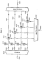
- Fig. 3 shows structural details of the loop-back device provided to each of the nodes, as a third embodiment.
- the loop-back device divides the received signal 1000 by the wavelength divider 2000 such that the optical signals of 1.53 ⁇ m, 1.54 ⁇ m, 1.55 ⁇ m, and 1.56 ⁇ m correspond to 1001 - 1004, and introduces the divided signals to the receiving side control signal receivers (RX) 1011 - 1014 and to spatial switches (SW) 1021 - 1024.
- RX receiving side control signal receivers
- SW spatial switches
- the number of the nodes is not limited to four as it can be larger or smaller.
- the bit rate for transmission is not limited to 10 Gb/s, and it may well be 1 Gb/s or 20 Gb/s, or larger or smaller.
- the topology of the network it is not limited to that of a star type as other topologies such as those of ring or mesh type may be employed.
- the first network in which the transmission and the reception are reversed is assumed to be the second network whereby, by utilizing one optical fiber network in both directions, two equivalent networks can come into existence.
- the signal wavelengths assigned to the optical transmitter are not limited to 1.53, 1.54, 1.55 and 1.56 ⁇ m as the wavelength such as 0.8 ⁇ m or 1.3 ⁇ m may be used as long as the necessary wavelength source can be obtained thereby.
- the wavelength interval to be set is not limited to 0.01 ⁇ m as it may be 1 nm or 0.1 ⁇ m, or larger or smaller. Also, it is possible to introduce optical amplifiers into the optical fiber networks for the compensation of loses.
- This switching means is required to have a function to set an input signal into one of three different modes, namely, being connected to the receiver line, connected to the loop-back line, and connected to none.
- the optical semiconductor gate switch is a semiconductor amplifier and has characteristics such that the light is allowed to pass when the injection current of several ten mA is applied, and the light is blocked when the injection current is intercepted.
- the injection current is applied (ON) to the semiconductor gate switch 403, and the injection current is intercepted (OFF) to the semiconductor gate switch 404.
- the semiconductor gate switch 404 For looping-back the signal, it is operated such that the semiconductor gate switch 404 is caused to be ON, and the semiconductor gate switch 403 is caused to be OFF. Further, when both the semiconductor gate switches 403 and 404 are caused to be OFF, the non-connected mode is realized.
Abstract
Description
- The present invention relates to an electrical communication system, and more particularly, though not exclusively, to an optical communication method and an optical communication network device for communication between a plurality of nodes, such as those between computers, or nodes within a computer.
- Electro-communication (or electrical communication) network technology for communication among a plurality of nodes is typically represented by conventional telephone network technology, which utilizes a system wherein a plurality of nodes and line exchange switches are interconnected and in which the line exchange switches monitor the state of congestion of the receiving side of the communication and this information on the state of congestion is transmitted to the communicated to the transmitting side of the communication as a part of the data communication media.
- In a network within a computer having a plurality of processors as nodes, the network is constituted by, as is the case in networks within a super computer, a coaxial cable line which connects each processor with a cross bar switch which controls communication among the processors. In such a network, when a processor transmits data to another processor, the data is first sent to the cross bar switch, and the cross bar switch feeds back to the transmitting side the state of congestion of a destination processor. When there is a congestion state, the transmission output is stopped and the outputted signal is stored in a buffer within the cross bar switch. Further, when the congestion state of the destination processor no longer exists, then this is detected and the data stored in the buffer is transmitted to the destination, and the control is carried out for the communication to be made with the processor for which the communication is requested.
- Each of the above two prior art network examples is a network in which the transmission volume is comparatively small, normally smaller than Gb/s. Thus, the network technology used is based on a conventional electrical network. However, recently, in view of the advancement in high speed operation of processors or the expansion in demands for an increased communication volume, extensive research is being made on optical networks utilizing optical communication techniques.
- The optical network technology, as typically represented by a large volume optical communication technology, can be used especially advantageously when applied as a technology for transmitting a large volume of data at once through one optical fiber. However, with the currently available technology, it is impossible to carry out the optical logical signal processing technology by the congestion control as carried out in electrical communication. Thus, the research is underway to solve this problem, and there is a proposal wherein, in media-access technology that has been employed in electrical communication, the same control channel is shared by nodes and, by using the control signal therefrom, the overall network control is carried out. This proposal is disclosed by P. A. Humblet, R. Ramaswami, and K. N. Sivarajan under the title "An Efficient Communication Protocol for High-Speed Packet-Switched Multichannel Networks", in IEEE Journal on Selected Areas in Communications, Vol. 11, No. 4, pp. 568 - 578, May 1993.
- With the use of the conventional electrical communication technology, the data transmission is becoming more difficult because of the problems presented by an increase in the data transmission volume and a lack of sufficient bands for transmission lines themselves. A further problem is that, since the control signal is extracted from the high speed data series, and the channel is controlled based on such a control signal, it is necessary to carry out a parallel process such as one in which the data is once time-divided and the resulting divided data are respectively subjected to switching processes. This results in requiring a large scale network.
- On the other hand, with the use of the optical network technology utilizing an optical communication technique, it is possible to readily increase the volume of transmitting data as explained above. However, since the method for controlling the optical network is based on the media access method that has been in use in the conventional electrical communication network process, it has been a problem that efficient network control is difficult to be carried out. If the architecture of the control system is made so as to be able to carry out efficient data transmission, then there are problems such that the synchronization of the overall network becomes necessary and that, since a new optical network becomes necessary for the control system, the cost of the overall system increases and resources such as optical devices cannot be effectively utilized. Also, in the switching optical devices, it becomes difficult to obtain a response larger than Gb/s because of the switching time, it becomes difficult to scale down the size of the device, and it becomes difficult to make integrated mounting in the fabrication of the device.
- Features of a communication method and an optical communication network device to be described below as examples are that it is possible to realize, by means of simple hardware, a communication network capable of achieving large volume data transmission, and that it is possible to control congestion by means of a simple control method.
- In one particular arrangement illustrative of the invention and to be described below, there is provided a method for communication using a network having a plurality of nodes, a first network medium connected to a first group of the plurality of nodes, and a second network medium being for transmitting control signals and connected to a second group of the plurality of nodes, the method comprising the steps of:
transmitting a transmission signal from any of the nodes to the first network medium when initiating data transmission, and
looping-back to the second network medium the transmission signal from a receiving node that has received the transmission signal such that information on a state of congestion at the receiving node is communicated. - The method of communication according to the first aspect of the invention is one in which, in a communication network having a plurality of nodes, the signal transmitted from the node is looped-back as it is through a control signal transmission medium. According to this method, unlike in the congestion control conventionally carried out, even when a large volume of data is transmitted, for example, in Gb/s bands, the device for the congestion control loops-back the received signal as it is. Thus, the feature of the network device is in dispensing with a large scale circuit required for complex processing such as the time division of the received data as employed in a conventional control system. For this reason, the communication system provided by the invention is simpler and more economical than that of the prior art.
- In another arrangement to be described below and illustrative of the invention, there is provided an optical communication network device having a plurality of nodes, a first optical fiber network connected to the nodes, and a second optical fiber network being for transmitting control signals and connected to the plurality of nodes, each of the nodes comprising:
a plurality of optical transmitters, a plurality of optical data receivers and a plurality of receiving side control signal receivers all of which are coupled to the first optical fiber network;
a plurality of switching means each of which recognizes an address data addressed to a receiving node from a signal received at the receiving side control signal receivers, and performs switching between looping-back of the signal received by the first optical fiber network as it is to the second optical fiber network and introducing of the signal received into the optical data receivers; and
a plurality of transmitting side control receivers which are coupled to the second optical fiber network . - An optical communication network device to be described below and illustrative of an aspect of the invention is, in one example, one in which each of the nodes has optical transmitters, optical receivers, receiving side control signal receivers, and transmitting side control signal receivers and in which, depending on a state of congestion at the receiving side, a signal transmitted from the optical transmitter is looped-back to the transmitting side through the control signal transmitting optical fiber network. In order to be able to transmit a large volume of data by making full use of the advantages of optical communication, it is necessary that the control of the optical communication network be simple and fast. In the prior art, a separate control channel is provided within the optical fiber network, and this channel is shared by a plurality of nodes for the transmission and reception of the control signal. Thus, each of the nodes requires a control signal optical transmitter and receiver in addition to that for data communication. However, according to the invention, such controlling is realized by a simple method wherein the signal transmitted from the transmitting side is looped-back as it is to the transmitting side through the loop-back means provided at the receiving side. Therefore, the network device according to the invention does not require such an optical transmitter for optical communication network control as required in the prior art optical communication network device, resulting in the reduction in cost of the overall communication network system and in the simplification of the device.
- A further feature of an optical communication network device to be described below, which is structured in a similar way to that of the aspect of the invention mentioned above, is that it is of a wavelength multiplex type, in which outputs of the optical transmitters provided respectively to the nodes have wavelengths different from one another.
- In this network device, the optical signal outputted to the first network can be recognized from its optical signal wavelength as to which node has outputted the signal and, since the signal looped-back from the receiving side is also of the same transmission wavelength and the transmitting side control signal receiver selectively receives only the signal of the wavelength outputted by the transmitting node, it is possible to loop-back to the transmitting side the state of congestion at any of the nodes within the network. For example, by adding the receiving side address data to a header of the transmitting signal, the receiving side may, if available for receiving the signal, discontinue looping-back the signal and, in this way, it is possible for the receiving side to inform the transmitting side of the reception availability state of the receiving side. According to the invention, since the signal transmitted from the transmitting side is looped-back, the network device is functionally equivalent to one in which there exist, at the receiving side, several light sources having different wavelengths for optical communication network control, and in which the state of congestion is transmitted to the transmitting side through the optical fiber networks for communication network control. Thus, as compared with one that has such light sources for multi-wavelengths optical communication network control, the device according to the invention is advantageous in that the cost of system is lower, the number of the devices required is smaller, and the system can be scaled down.
- Yet another aspect of an optical communication network device to be described below in illustrating the invention and that is structured in a similar way to the device described above, is that the switching means provided respectively to the nodes comprise optical semiconductor gate switches.
- In yet another arrangement illustrative of the invention, it is arranged that at the receiving side of each node, the signal transmitted from the transmitting side is switched either to be looped-back or to be led to the receiver, and this is realized by the optical semiconductor gate switches. Advantages in this construction are that the signal received can be switched at such a high speed as on the order of nanoseconds and that a compact device can be realized by the integration of a large number of optical switches for switching operations. The device can be significantly scaled down as compared with, for example, a lithium niobate waveguide type optical switch, and the voltage required for the switching is also significantly reduced.
- An optical communication network device which will be described below, which is structured in a similar way to that described above, and which is illustrative of the invention, has, in the transmitting side control signal receivers provided respectively to the nodes, filter means for selectively receiving only the signal transmitted from the optical transmitter of a transmitting node.
- In yet another arrangement illustrative of the invention, the transmitting node transmits signals having different wavelengths corresponding respectively to different nodes, and these signals are looped-back as they are through the control signal transmitting network for informing the state of congestion at the receiving side. Therefore, for the transmitting node to monitor the state of congestion of the receiving side, it is sufficient to provide only one control signal receiver that monitors the wavelength of the signal transmitted by the transmitting node. In this way, the architecture of the system is easy and is of low cost as compared with the conventional device that receives a large number of control signals. Here, the recognition of different nodes depends on the wavelengths, but it is possible to attain the same by other means, such as by a sub-carrier system whereby a change is made in signal receiving bands for recognizing differing nodes.
- Another particular example which illustrates the invention has an optical communication network device in which each of the optical semiconductor gate switches are arranged such that they function also as the receiving side control signal receiver.
- In this device, the optical semiconductor gate switch is shared by the receiving side as a transmitting signal detecting monitor. Normally, the optical semiconductor gate switch employs a traveling-wave type semiconductor amplifier. Such an optical semiconductor gate switch functions as a gate switch such that it allows signals to pass through when the injected current is flowing, and intercepts signals when the injected current is not flowing. On the other hand, the inter-electrode voltages undergo changes depending on whether the current is present or non-present so that it is possible to monitor the presence and non-presence by monitoring the inter-electrode voltages of the optical semiconductor gate switch. By using this theory, it is possible to cause the optical semiconductor gate switch to operate as the gate switch and, at the same time, as the control signal receiver for monitoring the presence and non-presence of the transmitted signal. This configuration results in reducing the number of the necessary optical devices in the entire system and also in reducing the cost of the system.
- The following description and drawings disclose, by means of an example, the invention which is characterised in the appended claims, whose terms determine the extent of the protection conferred hereby.
- In the drawings:-
- Fig. 1 is a structural diagram of an optical communication network of a first embodiment illustrative of the invention;
- Fig. 2 is a structural diagram of an optical communication network of a second embodiment illustrative of the invention;
- Fig. 3 is a diagram showing an arrangement of a loop-back device provided to each of the nodes, as a third embodiment illustrative of the invention;
- Fig. 4 is a diagram showing an arrangement of a switching means provided to each of the nodes, as a fourth embodiment illustrative of the invention;
- Figs. 5A and 5B are diagrams showing arrangements of control signal receiver structures, as a fifth embodiment illustrative of the invention, Fig. 5A showing a structure in which different wavelengths are assigned and Fig. 5B showing a structure in which different sub-carrier frequencies are provided; and
- Fig. 6 is a diagram showing an arrangement of an optical semiconductor gate switch which is shared by a receiving side control receiver, as a sixth embodiment illustrative of the invention.
- A structure of a first embodiment is explained with reference to Fig. 1. As shown therein, a plurality of nodes (N) 1, 2, 3 and 4 are interconnected in a ring form by a
network 10 that is a first network medium interconnecting them. Thenodes 1, 2, 3 and 4 respectively havecorresponding nodes second network medium 20 for controlling signal transmission. Thesecond network medium 20 is in a star configuration. Further, thenodes nodes 2 and 12, nodes 3 and 13, andnodes 4 and 14 are respectively interconnected bycircuits - The operation of the above communication system is now explained. Each of the nodes is structured so as to transfer data at a rate of 150 Mb/s to another node within the network. The operation explained here relates to the case where the
node 1 transfers data to the node 3. First, thenode 1 sends a signal to a receiving side address using a sub-carrier signal which overlaps afrequency 1 kHz assigned in advance to each node in thenetwork 10. Each node operates such that it detects the signal transmitted by thenetwork 10, demodulates the sub-carrier signal and transmits the signal as it is to the next node. Where the sub-carrier signal transmitted to a receiving node is the signal addressed to the node itself, this node operates so as to loop-back to the transmitting side a congestion state of the receiving node. That is, the address signal sent to thenetwork 10 from thenode 1 is transmitted to the node 2 which recognizes that the signal is not intended therefore and transmits the signal as it is to the node 3. The node 3 recognizes that the signal transmitted thereto from the node 2 is intended to its address and transmits this signal as it is to the node 13 through the loop-back circuit 18. The node 13 loops-back through the network 20 a loop-back signal to thenode 11 coupled to the transmittingside node 1. In this case, if the node 3 is in a congested state, the loop-back signal is sent out and, if the node is not in such a state, the control is made so as not to send back the loop-back signal. In this way, if the loop-back signal is not returned through thenode 11 within a certain time period, thenode 1 will judge that the receiving side node 3 is available for the reception of the signal, and can start the data transmission. As long as the node 3 keeps on returning the loop-back signal, the control for congestion is in effect so that the unavailability for the reception at the receiving side node 3 is looped-back to thenode 1. - In the above communication system, when the receiving side informs the transmitting side of a state of congestion of the receiving side, the receiving side is not required to carry out any high speed signal processing, and the control of congestion can be effected only by means of simple switching of the loop-back signals.
- In this embodiment, various modifications can be thought of. For example, the number of the nodes connected by the first and second networks is not limited to four as it can be larger or smaller. The structure of each of the first and second networks is not limited to that of a ring or a star type, and it may be of other topologies including a mesh type. The bit rate to be transmitted is not limited to 150 Mb/s, and it may well be 100 Mb/s or 1 Gb/s, or larger or smaller. Also, the volume of data transmitted from respective nodes does not need to be the same and the transmission can be made at different data rates. The system for transmitting address signals to a receiving side address is not limited to a sub-carrier system, and the transmission may be by time multiplexed data or code multiplexed data such as CDMA (Code Division Multi-Access) in so far as the signal looped-back can be recognized as being the data transmitted from the transmitting node. Further, the means to transmit data concerning a state of congestion at the receiving side is not limited to one based on whether the loop-back signal is present, and the loop-back signal may be transmitted after being modulated, or any other means may serve the purpose as long as the transmitting side can be informed of the state of congestion of the receiving side.
- Next, a second embodiment is explained with reference to Fig. 2.
- The optical communication network device of this embodiment is structured as explained hereinafter. A plurality of nodes are paired by optical transmitting
sections sections optical fiber network 101 in a star configuration. Also, the respective nodes are interconnected through a secondoptical fiber network 201 of a star configuration for looping-back a control signal from the receiving side to the transmitting side. Further, the respective nodes are constituted by optical transmitters (TX) 61, 62, 63 and 64, optical data receivers (RX) 161, 162, 163 and 164, receiving side control signal receivers (RX) 181, 182, 183 and 184, switching means (SW) 171, 172, 173 and 174, loop-back signal controllers (CTL) 191, 192, 193 and 194 for controlling the loop-back device by using control signals received at the receiving side control signal receivers, transmitting side control signal receivers (RX) 71, 72, 73 and 74 for receiving the loop-back signals through the secondoptical fiber network 201, and controllers (CTL) 81, 82, 83 and 84 for controlling the optical transmitters by using optical signals received at the transmitting side control signal receivers. According to one mode of this embodiment, the output wavelengths of the optical transmitters are set to wavelengths different from one another, as 1.53 µm, 1.54 µm, 1.55 µm, and 1.56 µm. - Fig. 3 shows structural details of the loop-back device provided to each of the nodes, as a third embodiment. The loop-back device divides the received
signal 1000 by thewavelength divider 2000 such that the optical signals of 1.53 µm, 1.54 µm, 1.55 µm, and 1.56 µm correspond to 1001 - 1004, and introduces the divided signals to the receiving side control signal receivers (RX) 1011 - 1014 and to spatial switches (SW) 1021 - 1024. The spatial switches 1021 - 1024 are such that, by the signals from the receiving side control signal receivers 1011 - 1014, they can be set in three different modes, that is, the optical signal being connected to the lines 1051 - 1054 coupled to the optical receivers, being connected to the lines 1061 - 1064 coupled to the loop-back lines, and being in a non-connected state with the lines 1071 - 1074 being open ended. The signals in the lines 1051 - 1054 outputted from the spatial switches 1021 - 1024 are wavelength multiplexed by awavelength multiplexer 2001 and then outputted to theline 3001 leading to the optical receiver, and the signals in the lines 1061 - 1064 are wavelength multiplexed by awavelength multiplexer 2002 and then outputted to the loop-back line 3002. When the switching means of the first node in the structure shown in Fig. 2 is taken as an example, theinput signal 300 therein corresponds to thesignal 1000 in Fig. 3, thesignal 301 to the optical receiver corresponds to thesignal 3001 in Fig. 3, and the loop-back signal 302 corresponds to thesignal 3002 in Fig. 3. - Now, the operation of the optical communication device structured as above and shown in Figs. 2 and 3 is explained. The operation is explained on an example wherein the request has been received for the data to be transmitted from the first node to the fourth node. In this case, the first node transmits to the
network 101 the address data of the fourth node at the wavelength of 1.53 µm by means of theoptical transmitter 61. Through thenetwork 101, the signal transmitted is inputted in the switching means 171 - 174 of each node and is simultaneously wavelength-divided, and the resulting signals are received by the control signal receivers 181 - 184. The control signal receivers 181 - 183, that is, in this example, the receiving sidecontrol signal receiver 1011, which are related to the wavelength of 1.53 µm, detects that there is a transmission request from the first node. However, they detect that the 1.53 µm signal does not include the address signal addressed to the first - third nodes, and so the switching means 171 - 173 are set to non-connected states. On the other hand, at the fourth node corresponding to the receiving node, thecontrol signal receiver 184 detects, by the receiving sidecontrol signal receiver 1011, the node address that is addressed to the fourth node. At this time, if theoptical receiver 164 of the fourth node is communicating with other nodes at different wavelengths, then the loop-back signal controller 194 connects the switching means 174 to the loop-back line, and loops-back through thenetwork 201 the address data of 1.53 µm wavelength that has been transmitted to the receiving node. If, on the other hand, the optical receiver of the fourth node is not communicating with other nodes, the loop-back signal controller 194 connects the switching means 174 to theoptical receiver 164, and controls the switching means 174 to switch for setting a reception stand-by state. - Now, it is assumed that, for example, after the above communication process has been completed and the first node and the fourth node has begun the communication at the data rate of 10 Gb/s, the second node has made a request to communicate with the fourth node. The second node sends out the address signal using the 1.54 µm wavelength by means of the
transmitter 62. This signal is wavelength-divided at the receiving side of the fourth node and is then detected by the receiving sidecontrol signal receiver 184. Since the fourth node is in communication with the first node, the switching means 174 is connected to the loop-back line, and the 1.54 µm wavelength signal is looped-back to the second node through thenetwork 201 whereby the congestion state of the fourth node is transmitted. - The arrangements explained above have made it possible to realize the optical communication network device which can easily transmit to the transmitting node the state of congestion at the receiving node.
- In this embodiment, various modifications can be thought of. For example, the number of the nodes is not limited to four as it can be larger or smaller. The bit rate for transmission is not limited to 10 Gb/s, and it may well be 1 Gb/s or 20 Gb/s, or larger or smaller. Further, it is not required for the entire network to be synchronized, and different nodes may transmit data at different bit rates. Instead of assigning different wavelengths to different transmission nodes, it is possible to assign frequency numbers of sub-carriers thereto. Further, as to the topology of the network, it is not limited to that of a star type as other topologies such as those of ring or mesh type may be employed. It is also possible to arrange such that the first network in which the transmission and the reception are reversed is assumed to be the second network whereby, by utilizing one optical fiber network in both directions, two equivalent networks can come into existence. Also, the signal wavelengths assigned to the optical transmitter are not limited to 1.53, 1.54, 1.55 and 1.56 µm as the wavelength such as 0.8 µm or 1.3 µm may be used as long as the necessary wavelength source can be obtained thereby. Further, the wavelength interval to be set is not limited to 0.01 µm as it may be 1 nm or 0.1 µm, or larger or smaller. Also, it is possible to introduce optical amplifiers into the optical fiber networks for the compensation of loses.
- Furthermore, if, instead of arranging the transmitting section and the receiving section in one node, the signal input side and the signal output side are made to correspond with each other, the resulting structure may be considered a switch which operates asynchronously. In this case, the structure can be caused to operate, for example, in an Asynchronous Transfer Mode (ATM) by providing a buffer which is explained later.
- Fig. 4 is a structural diagram for explaining a fourth embodiment of the invention. This embodiment is featured in that, in the loop-back system shown in Fig. 3, use is made of an optical semiconductor gate switch.
- The structure of the fourth embodiment is explained with reference to Fig. 4 which shows an arrangement of a switching means provided to each of the nodes. The function of the switching means is equivalent to that of the
spatial switch 1021 in Fig. 3. With this switching means, theoptical signal 400 inputted is split into two signals by anoptical splitter 402, and split signals are led to the optical semiconductor gate switches (SW) 403 and 404, respectively. The optical signal having passed through the opticalsemiconductor gate switch 403 becomes anoptical receiver signal 401, and the optical signal having passed through the opticalsemiconductor gate switch 404 becomes a loop-back signal 405. - Now, the operation of the switching means is explained. This switching means is required to have a function to set an input signal into one of three different modes, namely, being connected to the receiver line, connected to the loop-back line, and connected to none. The optical semiconductor gate switch is a semiconductor amplifier and has characteristics such that the light is allowed to pass when the injection current of several ten mA is applied, and the light is blocked when the injection current is intercepted. Thus, for connecting the
input signal 400 to the receiver side, the injection current is applied (ON) to thesemiconductor gate switch 403, and the injection current is intercepted (OFF) to thesemiconductor gate switch 404. For looping-back the signal, it is operated such that thesemiconductor gate switch 404 is caused to be ON, and thesemiconductor gate switch 403 is caused to be OFF. Further, when both the semiconductor gate switches 403 and 404 are caused to be OFF, the non-connected mode is realized. - Where the optical semiconductor gate switch described above is used, by applying a small current such as several ten mA, it is possible to cause the switching means to be operated, and by using a semiconductor element; it is possible to obtain a compact switching structure.
- Figs. 5A and 5B are structural diagrams for a fifth embodiment. The embodiment relates to a control signal receiver structure by which the signal looped-back is detected from the second optical fiber network. Illustrated herein are details of the transmitting side control signal receivers 71 - 74 shown in Fig. 2.
- The receiver shown in Fig. 5A is one in which, when the different wavelengths are assigned to the transmitting side as in the case of the third embodiment, the address signals assigned to respective nodes are received as loop-back signals. Here, one example is shown of the structure of the transmitting side control signal receiver which corresponds to the
node 1. The control signal receiver is configured such that the signal having passed through an optical band pass filter (λi) 501 having a bandwidth of 2 nm with its center being 1.53 µm which corresponds to the wavelength of 1.53 µm of the signal transmitted from thenode 1 is received by an optical receiver (RX) 502 and transmitted to a signal controller (CTL) 503. In this way, the looped-back signal of the signal transmitted from thenode 1 is selectively received easily. - Fig. 5B is a structural diagram of a typical loop-back control signal receiver in which different sub-carrier frequencies are provided at the transmitting side. This is structured such that the loop-back signal is first optically received by an optical receiver (RX) 511, and then is filtered by an electrical filter (fi) 512 for passing sub-carrier frequencies of the signal transmitted from the
node 1. The filtered signal is received by a signal controller (CTL) 513. - As explained above, by arranging so that the respective transmission signals are transmitted by using different wavelengths or different sub-carriers, it is possible to structure the control signal receiver such that the looped-back signals are easily selectively received.
- In this embodiment too, there can be various modifications that can be thought of. For example, the filter bandwidth for filtering wavelengths is not limited to 2 nm as it can be larger or smaller as long as the signals from other nodes can be distinguished. Also, the filter does not have to be the band pass filter as described. Further, the filter for selectively extracting a sub-carrier signal can be any electrical filter if capable of receiving signals selectively. There is also a possibility for a signal from a node to be distinguished from signals from other nodes by using codes such as CDMA.
- Fig. 6 is a structural diagram for a sixth embodiment.
- This embodiment is featured in an arrangement wherein the optical semiconductor gate switch shown in Fig. 4 is shared also as the receiving side control receiver. In this embodiment, the spatial switches 1021 - 1024 and the control signal receivers 1011 - 1014 as shown in Fig. 3 are indispensable at the receiving side. Thus, the idea here is to receive the control signal by using a terminal voltage of the optical semiconductor gate switch which exists in each of the spatial switches.
- This embodiment makes use of a semiconductor
optical amplifier 601. The terminal voltage of theoptical amplifier 601 is detected by avoltage monitor 602 and, at the same time, is bias-controlled by adriver circuit 603. When the terminal voltage is monitored, thedriver circuit 603 sets the optical amplifier to a reverse bias state, and the same operation as that of an ordinary optical detector is carried out. On the other hand, when the semiconductor optical amplifier is made ON from the signal received, it is possible to set theoptical amplifier 601 to a forward bias for carrying out the switching operation. - In this embodiment, too, various modifications are available. Here, for switching the optical semiconductor gate, the bias voltages are varied so as to monitor the terminal voltages. However, it is possible to carry out the monitoring under a non-bias state without the bias control.
- As methods for communication, the operations of the device shown in Fig. 2 include the following:
- (1) After the transmitting side transmits the address of the receiving side through the first optical fiber network, the receiving side loops-back a state of congestion and, when it is confirmed that there is no congestion at the receiving side, the transmitting side starts the communication. When this communication procedure is used, the time during which the transmitting side can confirm the state of congestion at the receiving side is no longer than about the time that is required for the loop-back signal to propagate, and this ensures establishing of high speed connections among the transmitting and receiving nodes. Also, for example, when the receiving side is congested and continues looping-back the signal transmitted, the transmitting side continues sending the address data of the receiving side as long as the signal is returned therefrom and, in this way, the information that the state of congestion has been released can be made known from the receiving side to the transmitting side by the interception of the looping-back signal. Also, when a number of transmission requests are simultaneously addressed to one receiving node, the receiving side schedules the sequence in which to receive the signals, and sequentially intercepts the looping-back signals, whereby the,signal reception schedule can be worked out in a simple manner.
- (2) In the above communication method, depending on communication procedures adopted, there is a possibility wherein the transmitting side may, before confirming the state of congestion of the receiving side, be unable to stop transmitting the signal. Under such a state, the device requires a data buffer which stores the transmitted data. In the optical communication network device of this configuration, if the buffer is provided at the receiving side, the size thereof is required to be large. However, where this is provided at the transmitting side, the size thereof can be made advantageously small. Further, where a number of such a communication network device are combined to form a large scale communication network, it may be arranged so that, after the state of congestion is looped-back from the receiving side to the transmitting side, if the buffer at the transmitting side is fully occupied, this information is looped-back to the transmitting side of the previous optical network stage and, in this way, it is possible to combine a plurality of optical networks or to make such networks in multiple stages.
In the above method, when the state of congestion at the receiving side is detected through the loop-back signal, the generation of the communication signal is stopped and, by applying a back-pressure, the data intended to be sent from the transmitting side is completely transmitted to the receiving side without loss of any data. - (3) In the procedure of transmitting the address signal from the transmitting side to the receiving side in the method explained above, it is arranged in advance that the data signal cycle of the transmittal signal be overlapped with the address signal. With this arrangement, simultaneously with the switching means being connected with the transmitting and receiving means, the communication can be started without the need of the operating time for establishing the synchronization among the transmitters and receivers.
- In the method explained above, by transmitting the signal that is set to the same data transmission rate as the address signal and is distinguishable on a bite to bite basis, it is made possible for the synchronization of the receiving side to be established simultaneously with the transmission of the address signal, so that the simultaneous connections can be established without requiring ensemble signal transmission as needed in a conventional method.
- While the invention has been described in its preferred embodiments, it is to be understood that the words which have been used are words of description rather than limitation and that changes within the purview of the appended claims may be made without departing from the true scope of the invention as defined by the claims.
Claims (9)
- A method for communication using a network having a plurality of nodes (1,2,3,4;11,12,13,14), a first network medium (10) connected to a first group (1,2,3,4) of said plurality of nodes, and a second network medium (20) being for transmitting control signals and connected to a second group (11,12,13,14) of said plurality of nodes, said method characterized by comprising the steps of:
transmitting a transmission signal from any of said nodes to said first network medium (10) when initiating data transmission, and
looping-back to said second network medium (20) said transmission signal from a receiving node that has received said transmission signal such that information on a state of congestion at said receiving node is communicated. - An optical communication network device having a plurality of nodes (1,2,3,4;11,12,13,14), a first optical fiber network (101) connected to said nodes, and a second optical fiber network (201) being for transmitting control signals and connected to said plurality of nodes, each of said nodes characterized by comprising:
a plurality of optical transmitters (61-64), a plurality of optical data receivers (161-164) and a plurality of receiving side control signal receivers (181-184) all of which are coupled to said first optical fiber network (101);
a plurality of switching means (171-174) each of which recognizes an address data addressed to a receiving node from a signal received at said receiving side control signal receivers, and performs switching between looping-back of the signal received by said first optical fiber network as it is to said second optical fiber network (201) and introducing of said signal received into said optical data receivers; and
a plurality of transmitting side control receivers (71-74) which are coupled to said second optical fiber network (201). - An optical communication network device according to claim 2, which is of a wavelength multiplex type and in which outputs of said optical transmitters (61-64) provided respectively to the nodes have wavelengths different from one another.
- An optical communication network device according to claim 2, in which said switching means provided respectively to the nodes comprise optical semiconductor gate switches (403, 404).
- An optical communication network device according to claim 2, in which said transmitting side control signal receivers provided respectively to the nodes comprise filter means for selectively receiving only the signal transmitted from the optical transmitter of a transmitting node.
- An optical communication network device according to claim 4, in which each of said optical semiconductor gate switches arranged such that they function also as said receiving side control signal receiver.
- A method for communication using an optical communication network device which is of a wavelength multiplex type and in which outputs of said optical transmitters (61-64) provided respectively to nodes have wavelengths different from one another, said method characterized by comprising the steps of:
transmitting an address data of a receiving node from a transmitting node by an optical transmitter to a first optical fiber network;
receiving by a receiving side control signal receiver the address data which is received from the first optical fiber network and which is transmitted from the transmitting node; and
looping-back by a loop back means to a second network (201) information on a state of congestion of the optical receiver of the receiving node. - A method for communication according to claim 7, in which, in the step of looping-back, a loop back signal from the receiving node is detected, and a request is made to the transmitting node to stop transmission and, if not possible to stop the transmission, the transmitted data is stored at a data buffer.
- A method for communication according to claim 7, in which a pattern of said address data includes a synchronization signal.
Applications Claiming Priority (3)
| Application Number | Priority Date | Filing Date | Title |
|---|---|---|---|
| JP6220078A JP2783164B2 (en) | 1994-09-14 | 1994-09-14 | Communication network |
| JP220078/94 | 1994-09-14 | ||
| JP22007894 | 1994-09-14 |
Publications (3)
| Publication Number | Publication Date |
|---|---|
| EP0702479A2 true EP0702479A2 (en) | 1996-03-20 |
| EP0702479A3 EP0702479A3 (en) | 1999-12-22 |
| EP0702479B1 EP0702479B1 (en) | 2002-11-27 |
Family
ID=16745595
Family Applications (1)
| Application Number | Title | Priority Date | Filing Date |
|---|---|---|---|
| EP95306447A Expired - Lifetime EP0702479B1 (en) | 1994-09-14 | 1995-09-14 | Optical communication system and method with separate medium for loop-back of congestion control information |
Country Status (3)
| Country | Link |
|---|---|
| US (1) | US5687013A (en) |
| EP (1) | EP0702479B1 (en) |
| JP (1) | JP2783164B2 (en) |
Cited By (14)
| Publication number | Priority date | Publication date | Assignee | Title |
|---|---|---|---|---|
| WO2001065887A2 (en) * | 2000-02-29 | 2001-09-07 | The Regents Of The University Of California | Ultra-low latency multi-protocol optical routers for the next generation internet |
| EP1185127A2 (en) * | 2000-08-29 | 2002-03-06 | KDDI Corporation | Reflection routing method in optical packet switching network and optical packet switch |
| US6522435B1 (en) | 1998-07-17 | 2003-02-18 | The Regents Of The University Of California | High-throughput, low-latency next generation internet networks using optical label switching and high-speed optical header generation, detection and reinsertion |
| US6525850B1 (en) | 1998-07-17 | 2003-02-25 | The Regents Of The University Of California | High-throughput, low-latency next generation internet networks using optical label switching and high-speed optical header generation, detection and reinsertion |
| US6580537B1 (en) | 1998-07-17 | 2003-06-17 | Regents Of The University Of California, The | High-throughput, low-latency next generation internet networks using optical label switching and high-speed optical header generation, detection and reinsertion |
| US6754450B2 (en) | 2001-01-30 | 2004-06-22 | The Regents Of The University Of California | Optical layer multicasting using a single sub-carrier header with active header detection, deletion, and new header insertion via opto-electrical processing |
| US6757497B2 (en) | 2001-01-30 | 2004-06-29 | The Regents Of The University Of California | Optical layer multicasting using a single sub-carrier header and a multicast switch with active header insertion via reflective single sideband optical processing |
| US6757496B2 (en) | 2001-01-30 | 2004-06-29 | The Regents Of The University Of California | Optical layer multicasting using a single sub-carrier header and an optical multicasting switch |
| US6768871B2 (en) | 2001-01-30 | 2004-07-27 | The Regents Of The University Of California | Optical layer multicasting using a multicast switch to effect survivability and security |
| US6813276B2 (en) | 2001-01-30 | 2004-11-02 | The Regents Of The University Of California | Optical layer multicasting using a single sub-carrier header with active header detection, deletion, and re-insertion via a circulating optical path |
| US6819666B2 (en) | 2001-01-30 | 2004-11-16 | The Regents Of The University Of California | Optical layer multicasting using multiple sub-carrier headers with header detection, deletion, and insertion via reflective single sideband optical processing |
| US6850707B1 (en) | 2001-01-30 | 2005-02-01 | The Regents Of The University Of California | Secure optical layer multicasting to effect survivability |
| US6850515B2 (en) | 2001-01-30 | 2005-02-01 | The Regents Of The University Of California | Optical layer multicasting using a single sub-carrier header and a multicast switch with active header insertion via light circulation |
| US6873797B2 (en) | 2001-01-30 | 2005-03-29 | The Regents Of The University Of California | Optical layer multicasting |
Families Citing this family (16)
| Publication number | Priority date | Publication date | Assignee | Title |
|---|---|---|---|---|
| FR2736777B1 (en) * | 1995-07-12 | 1997-08-08 | Alcatel Nv | OPTICAL TRANSMISSION NETWORK WITH WAVELENGTH MULTIPLEXING |
| JP3055452B2 (en) * | 1996-01-10 | 2000-06-26 | 日本電気株式会社 | Optical transmission line monitoring method |
| US6130876A (en) * | 1997-09-24 | 2000-10-10 | At&T Corp | Method and apparatus for restoring a network |
| US6052760A (en) * | 1997-11-05 | 2000-04-18 | Unisys Corporation | Computer system including plural caches and utilizing access history or patterns to determine data ownership for efficient handling of software locks |
| US6014709A (en) * | 1997-11-05 | 2000-01-11 | Unisys Corporation | Message flow protocol for avoiding deadlocks |
| US6092156A (en) * | 1997-11-05 | 2000-07-18 | Unisys Corporation | System and method for avoiding deadlocks utilizing split lock operations to provide exclusive access to memory during non-atomic operations |
| US6314501B1 (en) | 1998-07-23 | 2001-11-06 | Unisys Corporation | Computer system and method for operating multiple operating systems in different partitions of the computer system and for allowing the different partitions to communicate with one another through shared memory |
| US6647208B1 (en) * | 1999-03-18 | 2003-11-11 | Massachusetts Institute Of Technology | Hybrid electronic/optical switch system |
| WO2000058832A1 (en) * | 1999-03-25 | 2000-10-05 | Chromatis Networks, Inc. | Fault protection in networks |
| US6590870B1 (en) * | 1999-08-25 | 2003-07-08 | Adtran Inc. | Transmission of alternating delimiter code to achieve byte alignment when using in-band digital code sequences to remotely provision network interface device terminating local loop |
| US6693877B1 (en) * | 1999-09-07 | 2004-02-17 | Motorola, Inc. | Data discard avoidance method |
| US7630597B2 (en) * | 2006-05-30 | 2009-12-08 | Rogers Communications Inc. | Master/slave multiple path optical switching device |
| JP5614327B2 (en) * | 2011-02-24 | 2014-10-29 | 日本電気株式会社 | Optical amplifier controller |
| US9847928B2 (en) * | 2014-09-30 | 2017-12-19 | Alcatel-Lucent Usa Inc. | Verifying connector placement via loopback schemas |
| US10797476B2 (en) * | 2018-03-09 | 2020-10-06 | Elbex Video Ltd. | Two way and four way cascading optical exchanges provide traffic control for variety of signals with emphasis to WiFi |
| US20230395124A1 (en) * | 2022-06-07 | 2023-12-07 | Micron Technology, Inc. | Timing adjustment for data input/output buffer circuits |
Citations (1)
| Publication number | Priority date | Publication date | Assignee | Title |
|---|---|---|---|---|
| US5301052A (en) * | 1991-01-24 | 1994-04-05 | Alcatel N.V. | Communication method and network using optical fibers with frequency multiplexing |
Family Cites Families (6)
| Publication number | Priority date | Publication date | Assignee | Title |
|---|---|---|---|---|
| EP0192795B1 (en) * | 1985-02-28 | 1989-08-02 | International Business Machines Corporation | Communication system comprising overlayed multiple-access transmission networks |
| JPH0638601B2 (en) * | 1985-11-13 | 1994-05-18 | 富士通株式会社 | Optical composite transceiver |
| US5253248A (en) * | 1990-07-03 | 1993-10-12 | At&T Bell Laboratories | Congestion control for connectionless traffic in data networks via alternate routing |
| GB2251148B (en) * | 1990-09-18 | 1995-04-12 | Fujitsu Ltd | Optical repeater having loop-back function |
| FR2689711B1 (en) * | 1992-04-03 | 1994-05-13 | France Telecom | TELECOMMUNICATIONS NETWORK. |
| JPH06350646A (en) * | 1993-06-08 | 1994-12-22 | Nec Corp | Optical wavelength selection control system |
-
1994
- 1994-09-14 JP JP6220078A patent/JP2783164B2/en not_active Expired - Lifetime
-
1995
- 1995-09-13 US US08/527,379 patent/US5687013A/en not_active Expired - Fee Related
- 1995-09-14 EP EP95306447A patent/EP0702479B1/en not_active Expired - Lifetime
Patent Citations (1)
| Publication number | Priority date | Publication date | Assignee | Title |
|---|---|---|---|---|
| US5301052A (en) * | 1991-01-24 | 1994-04-05 | Alcatel N.V. | Communication method and network using optical fibers with frequency multiplexing |
Non-Patent Citations (3)
| Title |
|---|
| BRACKETT C A: "DENSE WAVELENGTH DIVISION MULTIPLEXING NETWORKS: PRINCIPLES AND APPLICATIONS" IEEE JOURNAL ON SELECTED AREAS IN COMMUNICATIONS, vol. 8, no. 6, 1 August 1990 (1990-08-01), pages 948-964, XP000208590 ISSN: 0733-8716 * |
| TOHRU MATSUNAGA: "SORTING-BASED ROUTING ALGORITHMS OF A PHOTONIC ATM CELL SWITCH: HIPOWER" IEEE TRANSACTIONS ON COMMUNICATIONS, vol. 41, no. 9, 1 September 1993 (1993-09-01), pages 1356-1363, XP000396695 ISSN: 0090-6778 * |
| YEUNG K L ET AL: "A WAVELENGTH CONCENTRATOR FOR WDMA NETWORKS" PROCEEDINGS OF THE GLOBAL TELECOMMUNICATIONS CONFERENCE (GLOBECOM), HOUSTON, NOV. 29 - DEC. 2, 1993, vol. 1, 29 November 1993 (1993-11-29), pages 144-148, XP000433044 INSTITUTE OF ELECTRICAL AND ELECTRONICS ENGINEERS * |
Cited By (21)
| Publication number | Priority date | Publication date | Assignee | Title |
|---|---|---|---|---|
| US6522435B1 (en) | 1998-07-17 | 2003-02-18 | The Regents Of The University Of California | High-throughput, low-latency next generation internet networks using optical label switching and high-speed optical header generation, detection and reinsertion |
| US6525851B2 (en) | 1998-07-17 | 2003-02-25 | The Regents Of The University Of California | High-throughput, low-latency next generation internet networks using optical label switching and high-speed optical header generation, detection and reinsertion |
| US6525850B1 (en) | 1998-07-17 | 2003-02-25 | The Regents Of The University Of California | High-throughput, low-latency next generation internet networks using optical label switching and high-speed optical header generation, detection and reinsertion |
| US6580537B1 (en) | 1998-07-17 | 2003-06-17 | Regents Of The University Of California, The | High-throughput, low-latency next generation internet networks using optical label switching and high-speed optical header generation, detection and reinsertion |
| US6657757B1 (en) | 1998-07-17 | 2003-12-02 | The Regents Of The University Of California | High-throughput low-latency next generation internet network using optical label switching and high-speed optical header generation detection and reinsertion |
| US6674558B1 (en) | 1998-07-17 | 2004-01-06 | The Regents Of The University Of California | High-throughput, low-latency next generation internet networks using optical label switching and high-speed optical header generation, detection and reinsertion |
| US6925257B2 (en) | 2000-02-29 | 2005-08-02 | The Regents Of The University Of California | Ultra-low latency multi-protocol optical routers for the next generation internet |
| WO2001065887A3 (en) * | 2000-02-29 | 2002-04-11 | Univ California | Ultra-low latency multi-protocol optical routers for the next generation internet |
| US6519062B1 (en) | 2000-02-29 | 2003-02-11 | The Regents Of The University Of California | Ultra-low latency multi-protocol optical routers for the next generation internet |
| WO2001065887A2 (en) * | 2000-02-29 | 2001-09-07 | The Regents Of The University Of California | Ultra-low latency multi-protocol optical routers for the next generation internet |
| EP1185127A2 (en) * | 2000-08-29 | 2002-03-06 | KDDI Corporation | Reflection routing method in optical packet switching network and optical packet switch |
| EP1185127A3 (en) * | 2000-08-29 | 2008-04-23 | KDDI Corporation | Reflection routing method in optical packet switching network and optical packet switch |
| US6754450B2 (en) | 2001-01-30 | 2004-06-22 | The Regents Of The University Of California | Optical layer multicasting using a single sub-carrier header with active header detection, deletion, and new header insertion via opto-electrical processing |
| US6768871B2 (en) | 2001-01-30 | 2004-07-27 | The Regents Of The University Of California | Optical layer multicasting using a multicast switch to effect survivability and security |
| US6813276B2 (en) | 2001-01-30 | 2004-11-02 | The Regents Of The University Of California | Optical layer multicasting using a single sub-carrier header with active header detection, deletion, and re-insertion via a circulating optical path |
| US6819666B2 (en) | 2001-01-30 | 2004-11-16 | The Regents Of The University Of California | Optical layer multicasting using multiple sub-carrier headers with header detection, deletion, and insertion via reflective single sideband optical processing |
| US6850707B1 (en) | 2001-01-30 | 2005-02-01 | The Regents Of The University Of California | Secure optical layer multicasting to effect survivability |
| US6850515B2 (en) | 2001-01-30 | 2005-02-01 | The Regents Of The University Of California | Optical layer multicasting using a single sub-carrier header and a multicast switch with active header insertion via light circulation |
| US6873797B2 (en) | 2001-01-30 | 2005-03-29 | The Regents Of The University Of California | Optical layer multicasting |
| US6757496B2 (en) | 2001-01-30 | 2004-06-29 | The Regents Of The University Of California | Optical layer multicasting using a single sub-carrier header and an optical multicasting switch |
| US6757497B2 (en) | 2001-01-30 | 2004-06-29 | The Regents Of The University Of California | Optical layer multicasting using a single sub-carrier header and a multicast switch with active header insertion via reflective single sideband optical processing |
Also Published As
| Publication number | Publication date |
|---|---|
| EP0702479B1 (en) | 2002-11-27 |
| EP0702479A3 (en) | 1999-12-22 |
| JP2783164B2 (en) | 1998-08-06 |
| US5687013A (en) | 1997-11-11 |
| JPH0884147A (en) | 1996-03-26 |
Similar Documents
| Publication | Publication Date | Title |
|---|---|---|
| EP0702479B1 (en) | Optical communication system and method with separate medium for loop-back of congestion control information | |
| US5550818A (en) | System for wavelength division multiplexing/asynchronous transfer mode switching for network communication | |
| EP0362790B1 (en) | Optical fiber communication method and multimedia opitcal fiber network using the same | |
| US5774244A (en) | Optical communications networks | |
| US5127067A (en) | Local area network with star topology and ring protocol | |
| US6295146B1 (en) | System and method for sharing a spare channel among two or more optical ring networks | |
| EP0593039B1 (en) | Optical concentrator and optical communication network using the same | |
| JP2002510441A (en) | Operation, protection and recovery method and apparatus for heterogeneous optical communication network | |
| US6111675A (en) | System and method for bi-directional transmission of telemetry service signals using a single fiber | |
| EP0857000A2 (en) | Optical transmission system | |
| JPH0799483A (en) | Communication system | |
| JPS63316957A (en) | Method and equipment for transmission in extra-high speed optical local area network | |
| US6262820B1 (en) | Optical transmission system including optical restoration | |
| US20070115805A1 (en) | Protection Switching Method and Apparatus for Nodes in a Resilient Packet Ring Network | |
| EP0859484B1 (en) | Fault restoration control method and it's apparatus in a communication network | |
| EP2582152B1 (en) | Remote node and network architecture and data transmission method for a fiber-optic network, especially for low bit-rate data transmission | |
| EP0533167A2 (en) | Optical communication system having transmission line switching system | |
| US20020105693A1 (en) | Optical transmission unit and system | |
| US7054555B2 (en) | Communication network, wavelength division multiplex transmission equipment, optical switch equipment, and optical attribute/state administering method for them | |
| JPH11122177A (en) | Monitor control signal transmitter and its method | |
| US7305184B2 (en) | Method and system for management of directly connected optical components | |
| JP3410576B2 (en) | Optical repeater monitoring system | |
| JPH05130034A (en) | Star ring communication equipment | |
| JP2002185405A (en) | Method for communicating optical signal by using operating ring and protective ring and optical node | |
| CN1428959A (en) | Double-way wave division multiplex optical network system |
Legal Events
| Date | Code | Title | Description |
|---|---|---|---|
| PUAI | Public reference made under article 153(3) epc to a published international application that has entered the european phase |
Free format text: ORIGINAL CODE: 0009012 |
|
| AK | Designated contracting states |
Kind code of ref document: A2 Designated state(s): FR GB SE |
|
| PUAL | Search report despatched |
Free format text: ORIGINAL CODE: 0009013 |
|
| AK | Designated contracting states |
Kind code of ref document: A3 Designated state(s): FR GB SE |
|
| RIC1 | Information provided on ipc code assigned before grant |
Free format text: 6H 04M 7/00 A, 6H 04M 3/36 B, 6H 04Q 3/58 B, 6H 04Q 11/00 B, 6H 04B 10/207 B |
|
| 17P | Request for examination filed |
Effective date: 19991124 |
|
| 17Q | First examination report despatched |
Effective date: 20001228 |
|
| GRAG | Despatch of communication of intention to grant |
Free format text: ORIGINAL CODE: EPIDOS AGRA |
|
| RTI1 | Title (correction) |
Free format text: OPTICAL COMMUNICATION SYSTEM AND METHOD WITH SEPARATE MEDIUM FOR LOOP-BACK OF CONGESTION CONTROL INFORMATION |
|
| RTI1 | Title (correction) |
Free format text: OPTICAL COMMUNICATION SYSTEM AND METHOD WITH SEPARATE MEDIUM FOR LOOP-BACK OF CONGESTION CONTROL INFORMATION |
|
| GRAG | Despatch of communication of intention to grant |
Free format text: ORIGINAL CODE: EPIDOS AGRA |
|
| GRAH | Despatch of communication of intention to grant a patent |
Free format text: ORIGINAL CODE: EPIDOS IGRA |
|
| GRAH | Despatch of communication of intention to grant a patent |
Free format text: ORIGINAL CODE: EPIDOS IGRA |
|
| GRAA | (expected) grant |
Free format text: ORIGINAL CODE: 0009210 |
|
| AK | Designated contracting states |
Kind code of ref document: B1 Designated state(s): FR GB SE |
|
| REG | Reference to a national code |
Ref country code: GB Ref legal event code: FG4D |
|
| PG25 | Lapsed in a contracting state [announced via postgrant information from national office to epo] |
Ref country code: SE Free format text: LAPSE BECAUSE OF FAILURE TO SUBMIT A TRANSLATION OF THE DESCRIPTION OR TO PAY THE FEE WITHIN THE PRESCRIBED TIME-LIMIT Effective date: 20030227 |
|
| ET | Fr: translation filed | ||
| PG25 | Lapsed in a contracting state [announced via postgrant information from national office to epo] |
Ref country code: GB Free format text: LAPSE BECAUSE OF NON-PAYMENT OF DUE FEES Effective date: 20030914 |
|
| PLBE | No opposition filed within time limit |
Free format text: ORIGINAL CODE: 0009261 |
|
| STAA | Information on the status of an ep patent application or granted ep patent |
Free format text: STATUS: NO OPPOSITION FILED WITHIN TIME LIMIT |
|
| 26N | No opposition filed |
Effective date: 20030828 |
|
| GBPC | Gb: european patent ceased through non-payment of renewal fee |
Effective date: 20030914 |
|
| PG25 | Lapsed in a contracting state [announced via postgrant information from national office to epo] |
Ref country code: FR Free format text: LAPSE BECAUSE OF NON-PAYMENT OF DUE FEES Effective date: 20040528 |
|
| REG | Reference to a national code |
Ref country code: FR Ref legal event code: ST |