EP0696010A1 - Portable interface for electronic chip card - Google Patents
Portable interface for electronic chip card Download PDFInfo
- Publication number
- EP0696010A1 EP0696010A1 EP95401641A EP95401641A EP0696010A1 EP 0696010 A1 EP0696010 A1 EP 0696010A1 EP 95401641 A EP95401641 A EP 95401641A EP 95401641 A EP95401641 A EP 95401641A EP 0696010 A1 EP0696010 A1 EP 0696010A1
- Authority
- EP
- European Patent Office
- Prior art keywords
- card
- housing
- module
- interface according
- interface
- Prior art date
- Legal status (The legal status is an assumption and is not a legal conclusion. Google has not performed a legal analysis and makes no representation as to the accuracy of the status listed.)
- Granted
Links
Images


Classifications
-
- G—PHYSICS
- G07—CHECKING-DEVICES
- G07F—COIN-FREED OR LIKE APPARATUS
- G07F7/00—Mechanisms actuated by objects other than coins to free or to actuate vending, hiring, coin or paper currency dispensing or refunding apparatus
- G07F7/08—Mechanisms actuated by objects other than coins to free or to actuate vending, hiring, coin or paper currency dispensing or refunding apparatus by coded identity card or credit card or other personal identification means
- G07F7/10—Mechanisms actuated by objects other than coins to free or to actuate vending, hiring, coin or paper currency dispensing or refunding apparatus by coded identity card or credit card or other personal identification means together with a coded signal, e.g. in the form of personal identification information, like personal identification number [PIN] or biometric data
- G07F7/1008—Active credit-cards provided with means to personalise their use, e.g. with PIN-introduction/comparison system
-
- G—PHYSICS
- G06—COMPUTING; CALCULATING OR COUNTING
- G06K—GRAPHICAL DATA READING; PRESENTATION OF DATA; RECORD CARRIERS; HANDLING RECORD CARRIERS
- G06K19/00—Record carriers for use with machines and with at least a part designed to carry digital markings
- G06K19/06—Record carriers for use with machines and with at least a part designed to carry digital markings characterised by the kind of the digital marking, e.g. shape, nature, code
- G06K19/067—Record carriers with conductive marks, printed circuits or semiconductor circuit elements, e.g. credit or identity cards also with resonating or responding marks without active components
- G06K19/07—Record carriers with conductive marks, printed circuits or semiconductor circuit elements, e.g. credit or identity cards also with resonating or responding marks without active components with integrated circuit chips
- G06K19/077—Constructional details, e.g. mounting of circuits in the carrier
- G06K19/07737—Constructional details, e.g. mounting of circuits in the carrier the record carrier consisting of two or more mechanically separable parts
- G06K19/07741—Constructional details, e.g. mounting of circuits in the carrier the record carrier consisting of two or more mechanically separable parts comprising a first part operating as a regular record carrier and a second attachable part that changes the functional appearance of said record carrier, e.g. a contact-based smart card with an adapter part which, when attached to the contact card makes the contact card function as a non-contact card
-
- G—PHYSICS
- G06—COMPUTING; CALCULATING OR COUNTING
- G06K—GRAPHICAL DATA READING; PRESENTATION OF DATA; RECORD CARRIERS; HANDLING RECORD CARRIERS
- G06K7/00—Methods or arrangements for sensing record carriers, e.g. for reading patterns
- G06K7/0013—Methods or arrangements for sensing record carriers, e.g. for reading patterns by galvanic contacts, e.g. card connectors for ISO-7816 compliant smart cards or memory cards, e.g. SD card readers
- G06K7/0021—Methods or arrangements for sensing record carriers, e.g. for reading patterns by galvanic contacts, e.g. card connectors for ISO-7816 compliant smart cards or memory cards, e.g. SD card readers for reading/sensing record carriers having surface contacts
-
- G—PHYSICS
- G06—COMPUTING; CALCULATING OR COUNTING
- G06K—GRAPHICAL DATA READING; PRESENTATION OF DATA; RECORD CARRIERS; HANDLING RECORD CARRIERS
- G06K7/00—Methods or arrangements for sensing record carriers, e.g. for reading patterns
- G06K7/0013—Methods or arrangements for sensing record carriers, e.g. for reading patterns by galvanic contacts, e.g. card connectors for ISO-7816 compliant smart cards or memory cards, e.g. SD card readers
- G06K7/0034—Methods or arrangements for sensing record carriers, e.g. for reading patterns by galvanic contacts, e.g. card connectors for ISO-7816 compliant smart cards or memory cards, e.g. SD card readers the connector being capable of simultaneously receiving a plurality of cards in the same insertion slot
-
- G—PHYSICS
- G06—COMPUTING; CALCULATING OR COUNTING
- G06K—GRAPHICAL DATA READING; PRESENTATION OF DATA; RECORD CARRIERS; HANDLING RECORD CARRIERS
- G06K7/00—Methods or arrangements for sensing record carriers, e.g. for reading patterns
- G06K7/0013—Methods or arrangements for sensing record carriers, e.g. for reading patterns by galvanic contacts, e.g. card connectors for ISO-7816 compliant smart cards or memory cards, e.g. SD card readers
- G06K7/0056—Methods or arrangements for sensing record carriers, e.g. for reading patterns by galvanic contacts, e.g. card connectors for ISO-7816 compliant smart cards or memory cards, e.g. SD card readers housing of the card connector
- G06K7/0073—Methods or arrangements for sensing record carriers, e.g. for reading patterns by galvanic contacts, e.g. card connectors for ISO-7816 compliant smart cards or memory cards, e.g. SD card readers housing of the card connector having multiple insertion slots, the respective slots suited for the same or different card form factors
-
- G—PHYSICS
- G06—COMPUTING; CALCULATING OR COUNTING
- G06Q—INFORMATION AND COMMUNICATION TECHNOLOGY [ICT] SPECIALLY ADAPTED FOR ADMINISTRATIVE, COMMERCIAL, FINANCIAL, MANAGERIAL OR SUPERVISORY PURPOSES; SYSTEMS OR METHODS SPECIALLY ADAPTED FOR ADMINISTRATIVE, COMMERCIAL, FINANCIAL, MANAGERIAL OR SUPERVISORY PURPOSES, NOT OTHERWISE PROVIDED FOR
- G06Q20/00—Payment architectures, schemes or protocols
- G06Q20/30—Payment architectures, schemes or protocols characterised by the use of specific devices or networks
- G06Q20/34—Payment architectures, schemes or protocols characterised by the use of specific devices or networks using cards, e.g. integrated circuit [IC] cards or magnetic cards
- G06Q20/341—Active cards, i.e. cards including their own processing means, e.g. including an IC or chip
-
- G—PHYSICS
- G07—CHECKING-DEVICES
- G07F—COIN-FREED OR LIKE APPARATUS
- G07F7/00—Mechanisms actuated by objects other than coins to free or to actuate vending, hiring, coin or paper currency dispensing or refunding apparatus
- G07F7/08—Mechanisms actuated by objects other than coins to free or to actuate vending, hiring, coin or paper currency dispensing or refunding apparatus by coded identity card or credit card or other personal identification means
- G07F7/0873—Details of the card reader
- G07F7/088—Details of the card reader the card reader being part of the point of sale [POS] terminal or electronic cash register [ECR] itself
- G07F7/0886—Details of the card reader the card reader being part of the point of sale [POS] terminal or electronic cash register [ECR] itself the card reader being portable for interacting with a POS or ECR in realizing a payment transaction
-
- Y—GENERAL TAGGING OF NEW TECHNOLOGICAL DEVELOPMENTS; GENERAL TAGGING OF CROSS-SECTIONAL TECHNOLOGIES SPANNING OVER SEVERAL SECTIONS OF THE IPC; TECHNICAL SUBJECTS COVERED BY FORMER USPC CROSS-REFERENCE ART COLLECTIONS [XRACs] AND DIGESTS
- Y10—TECHNICAL SUBJECTS COVERED BY FORMER USPC
- Y10S—TECHNICAL SUBJECTS COVERED BY FORMER USPC CROSS-REFERENCE ART COLLECTIONS [XRACs] AND DIGESTS
- Y10S439/00—Electrical connectors
- Y10S439/945—Adapter for pcb or cartridge
Definitions
- the present invention relates to a portable interface for one or more electronic smart cards, said interface ensuring the connection between electronic smart cards with a card reader of the type comprising a box of substantially rectangular rectangle shape ending in a plug connector with pins. in the reader, such as for example cards of the PCMCIA type.
- smart cards will be used to designate rectangular cards well known to the general public, such as bank cards, prepayment cards (for the public telephone for example), access cards to premises, etc. ...
- the format of these cards is standardized; the microchip is located at a specific location on the main surface of the card and its dimensions are approximately 85 x 54 x 1 mm.
- PCMCIA card is understood to mean not only all cards which are effectively compliant with the PCMCIA standard, but also all similar cards, of substantially rectangular rectangular shape, terminated at one end by a connector.
- the present invention provides a portable interface between one or more smart cards and a card reader of the PCMCIA type which does not have the drawbacks of the systems of the prior art.
- the guide and positioning means are advantageously constituted by the lateral edges, by the upper and lower internal surfaces and through the bottom of the housing.
- the housing can either be entirely contained inside the end piece or pass right through the end piece extending into the module.
- the interface according to the invention may include two or more superimposed housings, each of which can accommodate a smart card.
- the housings can be oriented along substantially parallel planes or along intersecting planes.
- a set of integrated circuits located in the module can be provided to connect the electrical connection means to the plug-in means for electrical connection with the card reader.
- the interface according to the invention can also comprise a single housing having a slot capable of accommodating several electronic chip cards.
- the housing becomes narrower along the length of the interface so that the smart cards inserted in the housing in use are offset with respect to each other.
- the module and the nozzle can advantageously be formed in one piece, for example a hollow plastic body molded in one piece and comprising a cover which can be metallic and of very thin thickness.
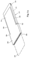
- the embodiment shown in Figures 1 allows to introduce a single smart card in the interface.
- the latter consists of a module which has the geometric shape and dimensions of a type 2 PCMCIA card.
- the embodiments shown and described below comprise a module having the external appearance of a type 2 PCMCIA card.
- the module 10 can have the appearance of a type 1, 2 and 3 PCMCIA card indifferently.
- PCMCIA type 1 cards have a rectangular shape with a thickness of 3.3 mm; those of type 2 have the same thickness of 3.3 mm at the edges but have an elevated central portion 14 delimited by the edges 30, the total thickness of the card at this location being 5 mm.
- the module comprises at one of its ends plug-in means 16 composed of a female pin with 68 connections.
- This pin 16 is pluggable into the male connection of the card reader (not shown).
- the length of the module 10 is approximately 8.5 cm and its width is approximately 5.4 cm. These dimensions correspond substantially to the dimensions of the smart cards.
- a tip 18 is fixed to the end of the module 10 opposite the connector 16. This tip 18 has the shape of a rectangular parallelepiped of the same thickness as the module 10 in its central part 14. The width of the tip 18 is slightly greater than that of module 10 and therefore greater than the width of a card of the PCMCIA type or of a smart card.
- the protrusions 20 and 22 of the endpiece form a stop against the face of the card reader when the interface is introduced into the reader.
- the end piece has a slot 24 which makes it possible to introduce a smart card 26 inside a housing 28 located in the end piece.
- the edges 12 of the central part 14 of the module 10 generally serve as means for guiding the PCMCIA card when it is inserted into the card reader.
- FIG. 1b and 1c are side and top views respectively of the embodiment shown in Figure 1a.
- the same elements have been represented by the same references (it will be the same subsequently for the other embodiments).
- Only the top of the interface is visible in Figure 1a; we see however in Figure 1b that the bottom of the interface has the same shape as the top.
- electrical connection means 32 intended to come into contact with electrical contact pads 33 of the chip card (FIG. 1c) .
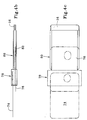
- the smart card 26 is inserted into the housing 28 (FIG. 1d and 1e) located in the end piece 18. This card is guided and positioned by means of guidance and positioning.
- the guiding and positioning means are constituted by the solid surfaces defining the housing itself, that is to say by the lateral edges 34 (FIG. 1e) of the housing 28 and by the upper 17 and lower 19 internal surfaces of the housing 28.
- the latter has a rectangular shape of width and height very slightly greater (by a few tenths of a millimeter) than that of the smart card 26 so that the card is guided when it is introduced.
- the depth of the housing 28 is large enough for the lateral edges 34 and the surfaces 17 and 19 to serve effectively as means for guiding and positioning the smart card inside the housing. This depth is advantageously equal to or greater than three centimeters.
- the bottom 36 of the housing 28 is used to position the smart card when the latter abuts against the bottom 36.
- a plurality of flush contactors 32 are located opposite and in contact with contact pads 33 located on the smart card surface.
- Each flush contactor 32 has the shape of an elastically deformable blade, integral with the end piece 18 and having a curved end for coming into contact with a region of the card.
- the contactors 32 are connected by electrical wires 37 to a printed circuit 38 housed inside the module 10.
- This printed circuit 38 comprises several electronic elements 40, such as integrated circuits.
- the connection between the printed circuit 38 and the connector 16 is preferably a direct link represented diagrammatically by 42 in FIGS. 1d and 1e, namely that the outputs of the printed circuit 30 are directly soldered to the terminals of connector 16.
- the printed circuit 38 with its electronic components 40 can fulfill different functions. First of all, it contains circuits dedicated to the electronic management of the smart card 26, as well as its power supply and clock signals. This management can be the exchange of data between the smart card and the device to which the interface is connected or the processing of the data provided by the smart card before the transfer of this data thus processed to the device to which is connected interface.
- the circuit can also fulfill other functions, such as storing information on mass memory or on solid state memory - volatile or not, increasing the memory capacity of the computer in which the interface is connected. or input-output functions such as network interfaces, telecommunications interfaces or interface with any other type of device.
- these additional functionalities can benefit from the simultaneous presence of one or more smart card (s) to, for example, ensure the security of access to data or networks, to verify rights of use, to sign or encrypt a transaction, or to pay for the use of the functions or services offered by the circuit.
- the module 10 and the end piece 18 form only one piece in order to increase the overall robustness of the interface.
- This part is advantageously molded in a plastic material in which the interior space of the module has been arranged to contain the printed circuit 38 with its components 40. This space is closed using a cover 44, preferably metallic and very thin, fixed to the module 10. This cover makes it possible to install the printed circuit 38 and to access this circuit if necessary.
- the housing 28 is also arranged in the plastic part formed by the module 10 and the end piece 18.
- the connectors 32 are pre-installed in the end piece 18 as well as the connecting wires 37.
- FIGS. 2a to 2e represent an embodiment of an interface ensuring the connection of two smart cards with a PCMCIA type card reader.
- the tip 46 has two slots 48 and 50 through which the smart cards 52 and 54 are inserted, respectively.
- the tip 46 is of greater thickness than in the embodiment of FIGS. 1. This thickness is approximately 1 cm.
- the module 10 is identical to that of FIGS. 1. It thus has the shape and the dimension of a type 2 PCMCIA type card, namely that its central part 14 is thicker (about 5 mm) than on the edges 12 of the module (about 3.3 mm). It also has at its end opposite to that of the module 46 a connector with plug-in pins 16.
- FIGS. 1 represents an embodiment of an interface ensuring the connection of two smart cards with a PCMCIA type card reader.
- the tip 46 has two slots 48 and 50 through which the smart cards 52 and 54 are inserted, respectively.
- the tip 46 is of greater thickness than in the embodiment of FIGS. 1. This thickness is approximately 1 cm.
- the module 10
- the end piece 46 comprises two housings 56 and 58 contained in the end piece 46. These housings have a rectangular shape and a width very slightly greater (by a few tenths of a millimeter) than the standardized width of smart cards ( Figures 2d and 2e). As a result, the lateral edges 60 and 62 of the two identical housings 56 and 58 serve as means for guiding and positioning the two smart cards 52 and 54.
- each of the two housings 56 and 58 is also used as a means of deep positioning.
- the electrical contact pads 66 are facing the flush contactors 68 and 70.
- the housings 56 and 58 are oriented in two parallel planes, so that the two cards 52 and 54 are parallel between them when they are introduced into the accommodation.
- Electrical wires 72 connect the contactors 68 70 to the printed circuit 38. This circuit contains electronic components 40 as indicated previously as well as connection contacts 42 with the pin of the plug-in connector 16.
- the end piece 46 and the module 10 are advantageously formed from a single molded part (in order to increase the robustness of the interface ), fitted with a cover 44.
- FIG. 3 represents an embodiment identical to that shown in FIGS. 2, except as regards the orientation of the housings 56 and 58 of the end piece 48.
- the two housings 56 and 58 are oriented along two intersecting planes.
- the two smart cards 52 and 54 are in two intersecting planes, converge on the module 10, so that the two outer ends of the two cards are distant from each other by a distance greater than the distance separating the two slots 48 and 50. In this way, it is easier to insert or remove the cards 52 and 54.
- FIGS. 4 makes it possible to connect two smart cards 74 and 76 to a card reader of the PCMCIA type. It differs from the embodiment shown in FIGS. 2 by the fact that one of the two housings intended to receive the smart cards is entirely contained in the end piece 78 while the other housing passes right through this end piece and extends into the module 80.
- the dimensions and the external shape of the interface are identical to those of the embodiment of FIG. 2.
- the module 80 likewise comprises a pin connector 16 and a central part 14 of thickness greater than the edges 12.
- the module 80 comprises a lateral slot 82 which allows the passage of the smart card 76. This slot is obviously necessary since the widths of the smart card and of the module 80 are substantially identical .
- the two housings 82 and 84 are situated in substantially parallel planes. One could of course easily imagine that this is not the case as in the embodiment of FIG. 3, the housing 82 then being inclined relative to the housing 84.
- the housing 82 is entirely contained in the end piece 78.
- the edges lateral, the upper and lower internal surfaces and the bottom of the housing serve as means for guiding and positioning the card 74 as in the previous embodiments.
- Flush electrical contactors 86 are placed in the housing 82 so that when the smart card 74 is in position, the contact pads 88 of the smart card are opposite the contactors 86. Electrical wires 90 connect the contactors 86 to the printed circuit 38 of the module 80.
- the housing 84 includes a first part 92 which passes right through the end piece 78 and which is extended by a part 94 in the module 80. In this part 94 there are flush contactors 96 which are located opposite the contact pads 98 of the smart card when the latter is in position in the housing 84. Electrical wires 100 connect the contactors 96 to the printed circuit 38. The contactors 96 can also be directly soldered to the printed circuit 38.
- the card 76 is guided during its introduction into the housing 84. using the side edges 102 and the upper 101 and lower 103 inner surfaces of the part 92 of the housing 84 located in the end piece 78. These edges 102 and these surfaces 101 and 103 are mutually parallel and located at a distance one from the other very slightly greater than the width and the thickness respectively of a smart card. The deep positioning of the card is carried out using the bottom 104 of the housing 84.
- the end piece 78 and the module 80 are formed in one piece, preferably made of molded plastic.
- FIG. 4 is particularly interesting when it is desired to use 2 smart cards simultaneously, one of which, the card 76, remains for a much longer time in the interface than the other card.
- the card 76 could be used for a whole day while the other card 74 would only be used for a relatively short period, for example ten minutes.
- the card 76 would remain permanently in the housing 84 while the housing 82 could successively accommodate a large number of smart cards.
- each of the housings 28, 56, 58, 82 or 84 of each of the embodiments described is advantageously provided with a micro-contact (not shown in the figures) which makes it possible to detect the presence and / or the correct positioning of the smart card in its slot.
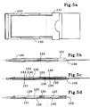
- Figures 5a, b, c, d show an evolution of the embodiment of Figure 4 in which there is only one housing adapted to receive the two smart cards.
- the interface includes a module 120 intended to be housed in a card reader, a tip 121 comprising a slot 122 capable of receiving the two cards, and a housing 123 in which the cards are positioned in use.
- the housing is made narrower at a point by means of a projection 124 which projects from the upper internal surface 125 of the housing and which divides the housing into two parts 126, 127.
- the projection 124, the lower internal surface 128 and the lateral edges of the housing serve to position a first card 130 in the housing as shown in FIG.
- the housing can be formed in two stages or with an upper internal surface which descends, for example, to make the space narrower towards the bottom of the housing and in order to offset the cards in the housing.
- the second card will be inserted into the slot between the upper surface of the first card and the upper internal surface of the housing which serve as guide means.
- the projection 124 serves to stop the progress of the card in the housing so that the card is positioned with its contact pads below the flush contacts 136 of the interface.
- a metal interlayer sheet (which is not shown in Figures 5) can be added to the housing to separate the housing into two parts and to guide the two cards.
- the sheet has a very thin thickness but is very rigid and is positioned in the horizontal plane between the two cards. As Figure 5a shows, the two cards pass through the end piece and extend into the module.
- the flush contacts 133 and 136 are connected to a printed circuit remained in the interface and to the terminals of a pin connector located at the end of the interface.
- the smart cards are offset in the housing and are oriented in the same direction with their contact pads facing the contactors flush in the upper internal surface of the housing. This embodiment has the advantage that the contactors are connected or integrated in a single printed circuit which is positioned above the housing in the interface.
- the contactors for the first or second card can be formed in the lower internal surface of the housing.
- the housing can have the same width everywhere, the cards being superimposed back to back in the housing with their contacts facing the flush contactors located in the upper and lower surfaces of the housing.
- the thickness of the end piece 18 could be greater than that of the module 10.
- the end piece 78 could contain several housings 82 superimposed on each other of so as to be able to simultaneously connect several smart cards 74 to the interface.
- the embodiments represented in FIGS. 2, 3 and 5 could be very easily modified so that more than two smart cards can be connected simultaneously with the interface.
- the embodiments described include a module which has the shape and dimensions of a type 2 PCMCIA card, but it is obvious that another type can be used.
- the interface module can take any other shape and size suitable for a card reader that is to be coupled with one or more smart cards.
Abstract
Description
La présente invention concerne une interface portable pour une ou plusieurs cartes à puce électronique, ladite interface assurant la liaison entre les cartes à puces électronique avec un lecteur de carte du type comportant un boîtier de forme sensiblement parallélipédique rectangle se terminant par un connecteur à broches enfichable dans le lecteur, telles que par exemple les cartes du type PCMCIA.The present invention relates to a portable interface for one or more electronic smart cards, said interface ensuring the connection between electronic smart cards with a card reader of the type comprising a box of substantially rectangular rectangle shape ending in a plug connector with pins. in the reader, such as for example cards of the PCMCIA type.
Par la suite on désignera par cartes à puce, les cartes de forme rectangulaire bien connues du grand public telles que les cartes bancaires, les cartes de prépaiement (pour le téléphone public par exemple), les cartes d'accès à des locaux, etc.... Le format de ces cartes est normalisé ; la puce électronique est située à un endroit précis sur la surface principale de la carte et ses dimensions sont d'environ 85 x 54 x 1 mm.Thereafter, smart cards will be used to designate rectangular cards well known to the general public, such as bank cards, prepayment cards (for the public telephone for example), access cards to premises, etc. ... The format of these cards is standardized; the microchip is located at a specific location on the main surface of the card and its dimensions are approximately 85 x 54 x 1 mm.
Il est de plus en plus courant d'utiliser à la place des disquettes pour ordinateurs, des cartes de mémoires électroniques ayant le format d'une carte à puce mais d'épaisseur plus grande. Le boîtier de ces cartes, de format sensiblement rectangulaire, est d'environ 85 mm par 54 mm, l'épaisseur étant uniformément de 3,3 mm (type 1), ou étant de 3,3 mm avec une partie centrale plus épaisse (5 mm, type 2) ou encore d'épaisseur 10 mm (type 3). L'extrémité du boîtier se termine par un connecteur du type femelle à 68 broches. Ce type de carte a été normalisée selon la norme dite PCMCIA qui signifie en anglais "Personal Computer Memory Card International Association". Ces mémoires sont très pratiques car d'une part leur format de poche les rend très facilement transportable et d'autre part elles peuvent avoir une capacité mémoire importante qui peut atteindre plusieurs dizaine de méga-octets. La plupart des matériels informatiques, et notamment des ordinateurs portables, comportent un lecteur de cates du type PCMCIA.It is more and more common to use instead of diskettes for computers, electronic memory cards having the format of a smart card but of greater thickness. The housing of these cards, of substantially rectangular format, is approximately 85 mm by 54 mm, the thickness being uniformly 3.3 mm (type 1), or being 3.3 mm with a thicker central part ( 5 mm, type 2) or 10 mm thick (type 3). The end of the case ends with a female 68-pin connector. This type of card has been standardized according to the so-called PCMCIA standard which means in English "Personal Computer Memory Card International Association". These memories are very practical because on the one hand their pocket format makes them very easily transportable and on the other hand they can have a large memory capacity which can reach several ten megabytes. Most computer equipment, including laptops, have a PCMCIA type reader.
Une fois enfiché dans le lecteur, la carte peut servir d'extension mémoire de l'ordinateur ou remplir d'autres fonctions telles que entrées/sorties, modem ou stockage de masse. Par la suite, on entend par carte PCMCIA, non seulement toutes les cartes qui sont effectivement conforme à la norme PCMCIA mais aussi toutes les cartes semblables, de forme sensiblement parallélipédique rectangle, terminées à une extrémité par un connecteur.Once plugged into the reader, the card can be used as a memory extension for the computer or perform other functions such as I / O, modem or mass storage. Subsequently, PCMCIA card is understood to mean not only all cards which are effectively compliant with the PCMCIA standard, but also all similar cards, of substantially rectangular rectangular shape, terminated at one end by a connector.
Du fait de l'utilisation de plus en plus répandue des cartes et des lecteurs du type PCMCIA, il s'est avéré utile de pouvoir faire lire par un lecteur du type PCMCIA des cartes à puce. Ces dernières comportent soit des circuits mémoire soit un microprocesseur associé à des circuits mémoire. Leur utilisation est de plus en plus étendue. Les cartes à puce et les cartes de type PCMCIA sont normalaisées aux mêmes dimensions : elles ont la même largeur et la même longueur. Mais leur épaisseur varie : l'épaisseur d'une carte à puce électronique est d'environ 1 mm alors que l'épaisseur d'une carte PCMCIA varie de 3,3 à 10 mm. Une autre différence réside dans le fait que les mémoires, sous forme de circuits intégrés, de la carte PCMCIA sont incluses à l'intérieur de la carte elle-même et la carte comporte à son extrémité un connecteur à broches, alors que la carte à puce comporte un circuit intégré et des plages de contact situés à des endroits bien précis sur la surface principale de la carte. Il en résulte que les lecteurs de carte PCMCIA ne peuvent pas lire les cartes à puce, et réciproquement, sans modification du lecteur.Owing to the increasingly widespread use of cards and readers of the PCMCIA type, it has proved useful to be able to have chip cards read by a reader of the PCMCIA type. These include either memory circuits or a microprocessor associated with memory circuits. Their use is more and more widespread. Smart cards and PCMCIA type cards are normalized to the same dimensions: they have the same width and the same length. But their thickness varies: the thickness of an electronic chip card is around 1 mm while the thickness of a PCMCIA card varies from 3.3 to 10 mm. Another difference lies in the fact that the memories, in the form of integrated circuits, of the PCMCIA card are included inside the card itself and the card has at its end a pin connector, while the card with puce has an integrated circuit and contact pads located in specific locations on the main surface of the card. As a result, PCMCIA card readers cannot read smart cards, and vice versa, without modifying the reader.
On connaît déjà des lecteurs de cartes particuliers qui permettent de lire indifféremment des cartes à puce et des cartes du type PCMCIA. Ces lecteurs comportent généralement un plateau, qui permet de s'adapter à la différence d'épaisseur des cartes, ainsi que des connecteurs électriques des deux types, soit PCMCIA, soit carte à puce. A titre d'exemple, la demande de brevet FR 2 687 238 et le brevet US 5 198 645 décrivent ce type de lecteur.Particular card readers are already known which allow smart cards and PCMCIA type cards to be read interchangeably. These readers generally include a tray, which makes it possible to adapt to the difference in thickness of the cards, as well as electrical connectors of the two types, either PCMCIA or smart card. For example, patent application FR 2 687 238 and US patent 5 198 645 describe this type of reader.
Une autre solution décrite dans la demande de brevet EP 0 552 078, consiste à diminuer l'épaisseur d'une carte PCMCIA et à l'équiper d'un connecteur supplémentaire à contacts affleurants sur sa face principale. On remarque que dans un tel système les deux cartes, carte à puce et carte PCMCIA, sont superposées dans le lecteur. Les deux cartes ayant la même largeur peuvent être guidées dans le lecteur de carte par le système de guidage et de positionnement du lecteur. Cependant ce dernier est conçu pour une carte de type PCMCIA et pas pour l'empilement d'une carte à puce avec une carte PCMCIA. Il s'en suit un manque de précision du positionnement de la carte à puce. De plus, lorsque l'on cherche à introduire la carte à puce dans un lecteur de carte contenant déjà une carte PCMCIA dont on a diminué l'épaisseur, il peut se produire des fausses manoeuvres dues au fait que l'espace restant pour accueillir la carte à puce est relativement réduit. On remarque également que l'espace disponible pour accueillir des composants électroniques, tels que des mémoires, à l'intérieur de la carte PCMCIA d'épaisseur réduite est largement diminuée par rapport à l'espace disponible dans une carte PCMCIA classique. On ne peut donc pas loger autant de composants électroniques à l'intérieur d'une carte d'épaisseur réduite que dans une carte d'épaisseur réduite que dans une carte PCMCIA d'épaisseur normale. De plus, un tel système ne permet de lire qu'une seule carte à puce alors que pour certaines applications plusieurs cartes auraient besoin d'être lues par le lecteur de carte simultanément.Another solution described in patent application EP 0 552 078 consists in reducing the thickness of a PCMCIA card and in equipping it with an additional connector with flush contacts on its main face. Note that in such a system the two cards, chip card and PCMCIA card, are superimposed in the reader. The two cards having the same width can be guided in the card reader by the guide and positioning system of the reader. However, the latter is designed for a PCMCIA type card and not for stacking a smart card with a PCMCIA card. The result is a lack of precision in the positioning of the smart card. In addition, when it is sought to introduce the chip card into a card reader already containing a PCMCIA card whose thickness has been reduced, there may be false operations due to the fact that the space remaining to accommodate the smart card is relatively small. It is also noted that the space available for accommodating electronic components, such as memories, inside the PCMCIA card of reduced thickness is greatly reduced compared to the space available in a conventional PCMCIA card. It is therefore not possible to accommodate as many electronic components inside a card of reduced thickness as in a card of reduced thickness than in a PCMCIA card of normal thickness. In addition, such a system only allows one smart card to be read, whereas for certain applications several cards would need to be read by the card reader simultaneously.
Une autre solution est proposée par le brevet US 5 296 692 qui décrit un adaptateur pouvant être inséré dans un lecteur. L'adaptateur comporte un réceptacle pouvant recevoir une carte du type PCMCIA et une carte à puce, ces cartes étant superposées, l'une au-dessus de l'autre. Il en résulte que la fente par laquelle on introduit les cartes a une largeur supérieure à celle des lecteurs de cartes classiques et que l'adaptateur n'a pas des dimensions standard et ne peut pas être utilisé directement avec un lecteur de cartes de type PCMCIA.Another solution is proposed by US patent 5,296,692 which describes an adapter which can be inserted into a reader. The adapter includes a receptacle which can receive a card of the PCMCIA type and a smart card, these cards being one above the other. As a result, the slot through which the cards are inserted has a width greater than that of conventional card readers and that the adapter does not have standard dimensions and cannot be used directly with a PCMCIA type card reader. .
La présente invention propose une interface portable entre une ou plusieurs cartes à puce et un lecteur de carte du type PCMCIA qui n'a pas les inconvénients des systèmes de l'art antérieur.The present invention provides a portable interface between one or more smart cards and a card reader of the PCMCIA type which does not have the drawbacks of the systems of the prior art.
L'invention propose une interface portable, enfichable dans un lecteur de carte comprenant :
- un module de forme sensiblement rectangulaire, destiné à être logé dans le lecteur de carte et comportant à une extrémité des moyens enfichables de liaison électrique avec ledit lecteur de carte;
- un embout solidaire de l'autre extrémité du module et de largeur supérieure à la largeur du module et comportant une fente pour l'introduction de la carte à puce;
- un logement de forme sensiblement plane, destiné à recevoir au moins partiellement la carte à puce et traversant au moins en partie ledit embout, à partir de ladite fente, ledit logement comportant des moyens de guidage et de positionnement de la carte à puce; et
- des moyens de connexion électrique avec lesdites plages de contact électrique de la carte à puce, lesdits moyens étant situés à l'intérieur de l'interface.
- a module of substantially rectangular shape, intended to be housed in the card reader and comprising at one end pluggable means for electrical connection with said card reader;
- an end piece integral with the other end of the module and of width greater than the width of the module and comprising a slot for the introduction of the smart card;
- a housing of substantially planar shape, intended to receive at least partially the smart card and at least partially passing through said end piece, from said slot, said housing comprising means for guiding and positioning the smart card; and
- electrical connection means with said electrical contact pads of the smart card, said means being located inside the interface.
Les moyens de guidage et de positionnement sont avantageusement constitués par les bords latéraux, par les surfaces internes supérieur et inférieure et par le fond du logement.The guide and positioning means are advantageously constituted by the lateral edges, by the upper and lower internal surfaces and through the bottom of the housing.
Le logement peut être soit entièrement contenu à l'intérieur de l'embout ou traverser de part en part l'embout en se prolongeant dans le module.The housing can either be entirely contained inside the end piece or pass right through the end piece extending into the module.
L'interface selon l'invention peut comporter deux ou plusieurs logements superposés, chacun d'eux pouvant accueillir une carte à puce. Les logements peuvent être orientés selon des plans sensiblement parallèles ou selon des plans sécants. Lorsque l'interface comporte deux logements, l'un peut être entièrement contenu à l'intérieur de l'embout alors que l'autre traverse de part en part l'embout en se prolongeant dans le module. Un ensemble de circuits intégrés situé dans le module peut être prévu pour relier les moyens de connexion électrique aux moyens enfichables de liaison électrique avec le lecteur de cartes.The interface according to the invention may include two or more superimposed housings, each of which can accommodate a smart card. The housings can be oriented along substantially parallel planes or along intersecting planes. When the interface has two housings, one can be entirely contained inside the end piece while the other passes right through the end piece, extending into the module. A set of integrated circuits located in the module can be provided to connect the electrical connection means to the plug-in means for electrical connection with the card reader.
L'interface selon l'invention peut également comprendre un seul logement ayant une fente apte à accueillir plusieurs cartes à puce électronique. De préférence, le logement devient plus étroit suivant la longeur de l'interface afin que les cartes à puce insérées dans le logement en utilisation soient décalées l'une par rapport à l'autre.The interface according to the invention can also comprise a single housing having a slot capable of accommodating several electronic chip cards. Preferably, the housing becomes narrower along the length of the interface so that the smart cards inserted in the housing in use are offset with respect to each other.
Le module et l'embout peuvent avantageusement être formés d'une seule pièce, par exemple un corps creux en plastique moulé d'une seule pièce et comprenant un couvercle qui peut être métallique et d'épaisseur très fine.The module and the nozzle can advantageously be formed in one piece, for example a hollow plastic body molded in one piece and comprising a cover which can be metallic and of very thin thickness.
L'invention sera mieux comprise à l'aide de la description qui suit de plusieurs modes de réalisation de l'invention faite en référence aux dessins qui l'accompagnent dans lesquels :
- les figures 1 représentent un mode de réalisation de l'invention qui permet d'introduire une seule carte à puce dans l'interface, la figure 1a étant une vue en perspective, les figures 1b et 1c représentant respectivement une vue de coté et de haut, et les figures 1d et 1e représentant des coupes selon deux plans perpendiculaires;
- les figures 2 représentent un mode de réalisation avec deux cartes à puce toutes deux logées uniquement dans l'embout et de façon parallèle, la figure 2a étant une vue en perspective, les figures 2b et 2c étant respectivement une vue de coté et de haut et les figures 2d et 2e représentant des coupes selon deux plans perpendiculaires;
- la figure 3 représente en perspective un mode de réalisation avec deux cartes à puce situées dans deux plans sécants;
- les figures 4 représentent un mode de réalisation de l'invention avec deux cartes, l'une étant logée dans l'embout uniquement et l'autre étant logée entièrement dans l'embout et en partie dans le module, la figure 4a étant une vue en perspective, les figures 4b et 4c une vue respectivement de coté et de haut et la figure 4d et 4e des coupes selon deux plans perpendiculaires;
- les figures 5 représentent un autre mode de réalisation avec deux cartes et ayant un seul logement pour les accueillir, la figure 5a étant une vue de haut, la figure 5b étant une vue de coté, et les figures 5c et 5d étant des coupes selon deux plans perpendiculaires, avec et sans cartes, respectivement.
- FIGS. 1 represent an embodiment of the invention which makes it possible to introduce a single smart card into the interface, FIG. 1a being a perspective view, FIGS. 1b and 1c respectively representing a side and top view , and Figures 1d and 1e showing sections along two perpendicular planes;
- FIGS. 2 represent an embodiment with two smart cards, both housed only in the end piece and in parallel, FIG. 2a being a perspective view, FIGS. 2b and 2c being respectively a side and top view and Figures 2d and 2e showing sections along two perpendicular planes;
- Figure 3 shows in perspective an embodiment with two smart cards located in two intersecting planes;
- FIGS. 4 represent an embodiment of the invention with two cards, one being housed in the end piece only and the other being housed entirely in the end piece and partly in the module, FIG. 4a being a view in perspective, FIGS. 4b and 4c are a side and top view respectively and FIG. 4d and 4e of the sections along two perpendicular planes;
- Figures 5 show another embodiment with two cards and having a single housing to accommodate them, Figure 5a being a top view, Figure 5b being a side view, and Figures 5c and 5d being sections according to two perpendicular planes, with and without maps, respectively.
Le mode de réalisation représenté sur les figures 1 permet d'introduire une seule carte à puce dans l'interface. Ce dernier est constitué d'un module qui a la forme géométrique et les dimensions d'une carte PCMCIA du type 2. Les modes de réalisations représentés et décrits par la suite comportent un module ayant l'aspect extérieur d'une carte PCMCIA type 2. Cependant le module 10 peut avoir l'aspect d'une carte PCMCIA du type 1, 2 et 3 indifféremment. Les cartes PCMCIA du type 1 ont une forme rectangulaire d'épaisseur 3,3 mm; celles du type 2 ont la même épaisseur de 3,3 mm sur les bords mais comportent une partie centrale 14 surélevée délimitée par les bords 30, l'épaisseur totale de la carte à cet endroit étant de 5 mm. Comme toute carte PCMCIA, le module comporte à l'une de ses extrémités des moyens enfichables 16 composés d'une broche femelle à 68 connexions. Cette broche 16 est enfichable dans la connexion mâle du lecteur de carte (non représenté). La longueur du module 10 est d'environ 8,5 cm et sa largeur est d'environ 5,4 cm. Ces dimensions correspondent sensiblement aux dimensions des cartes à puce. Un embout 18 est fixé à l'extrémité du module 10 opposé au connecteur 16. Cet embout 18 a la forme d'un parallélépipède rectangle de même épaisseur que le module 10 dans sa partie centrale 14. La largeur de l'embout 18 est légèrement supérieure à celle du module 10 et donc supérieure à la largeur d'une carte du type PCMCIA ou d'une carte à puce. Les parties saillantes 20 et 22 de l'embout forment une butée contre la face du lecteur de carte lorsque l'interface est introduite dans le lecteur. L'embout comporte une fente 24 qui permet d'introduire une carte à puce 26 à l'intérieur d'un logement 28 situé dans l'embout. Les bords 12 de la partie centrale 14 du module 10 servent généralement de moyens de guidage de la carte PCMCIA lors de son introduction dans le lecteur de carte.The embodiment shown in Figures 1 allows to introduce a single smart card in the interface. The latter consists of a module which has the geometric shape and dimensions of a type 2 PCMCIA card. The embodiments shown and described below comprise a module having the external appearance of a type 2 PCMCIA card. However, the
Les figures 1b et 1c sont des vues respectivement de coté et de haut du mode de réalisation représenté sur la figure 1a. Les mêmes éléments ont été représentés par les mêmes références (il en sera de même par la suite pour les autres modes de réalisation). Seul le dessus de l'interface est visible sur la figure 1a; on s'aperçoit cependant sur la figure 1b que le dessous de l'interface a la même forme que le dessus. On retrouve donc une partie centrale 14 du module 10 qui est plus épaisse que les bords 12. Sur la figure 1b apparaissent des moyens de connexion électrique 32 destinés à venir en contact avec des plages de contact électrique 33 de la carte à puce (figure 1c).Figures 1b and 1c are side and top views respectively of the embodiment shown in Figure 1a. The same elements have been represented by the same references (it will be the same subsequently for the other embodiments). Only the top of the interface is visible in Figure 1a; we see however in Figure 1b that the bottom of the interface has the same shape as the top. We therefore finds a
La carte à puce 26 est introduite dans le logement 28 (figure 1d et 1e) situé dans l'embout 18. Cette carte est guidée et positionnée par des moyens de guidage et de positionnement.The
Dans les exemples illustrés dans les figures, les moyens de guidage et de positionnement sont constitués par les surfaces solides définissant le logement lui-même, c'est-à-dire par les bords latéraux 34 (figure 1e) du logement 28 et par les surfaces internes supérieure 17 et inférieure 19 du logement 28. Ce dernier a une forme rectangulaire de largeur et de hauteur très légèrement supérieure (de quelques dixièmes de millimètres) à celle de la carte à puce 26 de sorte que la carte est guidée lorsqu'elle est introduite. La profondeur du logement 28 est suffisamment grande pour que les bords latéraux 34 et les surfaces 17 et 19 servent de façon efficace de moyens de guidage et de positionnement de la carte à puce à l'intérieur du logement. Cette profondeur est avantageusement égale ou supérieure à trois centimètres. Le fond 36 du logement 28 sert à positionner la carte à puce lorsque cette dernière vient en butée contre le fond 36. Dans ce cas, une pluralité de contacteurs affleurants 32 sont situés en regard et en contact avec des plages de contact 33 situées sur la surface de la carte à puce. Chaque contacteur affleurant 32 a la forme d'une lame élastiquement déformable, solidaire de l'embout 18 et présentant une extrémité incurvée pour entrer en contact avec une plage de la carte. Les contacteurs 32 sont reliés par des fils électriques 37 à un circuit imprimé 38 logé à l'intérieur du module 10. Ce circuit imprimé 38 comprend plusieurs éléments électroniques 40, tels que des circuits intégrés. La liaison entre le circuit imprimé 38 et le connecteur 16 est de préférence une liaison directe représentée schématiquement par 42 sur les figures 1d et 1e, à savoir que les sorties du circuit imprimé 30 sont directement soudés aux bornes du connecteur 16.In the examples illustrated in the figures, the guiding and positioning means are constituted by the solid surfaces defining the housing itself, that is to say by the lateral edges 34 (FIG. 1e) of the
Le circuit imprimé 38 avec ses composants électroniques 40 peut remplir différentes fonctions. Tout d'abord, il contient des circuits dédiés à la gestion électronique de la carte à puce 26, ainsi que son alimentation électrique et signaux d'horloge. Cette gestion peut être l'échange de données entre la carte à puce et l'appareil auquel l'interface est connectée ou encore le traitement des données fournies par la carte à puce avant le transfert de ces données ainsi traitées à l'appareil auquel est connectée l'interface.The printed
Le circuit peut également remplir d'autres fonctions, telles que le stockage d'information sur mémoire de masse ou sur mémoire à état solide - volatiles ou non, l'augmentation de la capacité mémoire de l'ordinateur dans lequel l'interface est connectée ou des fonctions d'entrées-sorties telles qu'interfaces réseau, interfaces de télécommunications ou interface avec tout autre type d'appareils. Dans ce cas, ces fonctionnalités supplémentaires peuvent bénéficier de la présence simultanée d'une ou plusieurs carte(s) à puce pour, par exemple, assurer la sécurisation de l'accès aux données ou aux réseaux, pour vérifier des droits d'utilisation, pour signer ou chiffrer une transaction, ou pour payer l'utilisation des fonctions ou services offerts par le circuit.The circuit can also fulfill other functions, such as storing information on mass memory or on solid state memory - volatile or not, increasing the memory capacity of the computer in which the interface is connected. or input-output functions such as network interfaces, telecommunications interfaces or interface with any other type of device. In this case, these additional functionalities can benefit from the simultaneous presence of one or more smart card (s) to, for example, ensure the security of access to data or networks, to verify rights of use, to sign or encrypt a transaction, or to pay for the use of the functions or services offered by the circuit.
Dans les modes de réalisation préférés et représentés sur les figures 1 à 4 le module 10 et l'embout 18 ne forment qu'une seule pièce afin d'augmenter la robustesse globale de l'interface. Cette pièce est avantageusement moulée dans une matière plastique dans laquelle on a aménagé l'espace intérieur du module pour contenir le circuit imprimé 38 avec ses composants 40. Cet espace est fermé à l'aide d'un couvercle 44, de préférence métallique et de très faible épaisseur, fixé sur le module 10. Ce couvercle permet de pouvoir installer le circuit imprimé 38 et d'accéder à ce circuit si nécessaire. Le logement 28 est également aménagé dans la pièce en plastique formé par le module 10 et l'embout 18. Les connecteurs 32 sont pré-installés dans l'embout 18 ainsi que les fils de jonction 37.In the preferred embodiments and shown in FIGS. 1 to 4, the
Dans le mode de réalisation de la figure 1, le logement 2 de la carte à puce est entièrement contenu à l'intérieur de l'embout 18. Les figures 2a à 2e représentent un mode de réalisation d'une interface assurant la connexion de deux cartes à puce avec un lecteur de carte du type PCMCIA. L'embout 46 comporte deux fentes 48 et 50 par lesquelles sont insérées les cartes à puce respectivement 52 et 54. L'embout 46 est d'épaisseur plus importante que dans le mode de réalisation des figures 1. Cette épaisseur est d'environ 1 cm. Le module 10 est identique à celui des figures 1. Il a ainsi la forme et la dimension d'une carte de type PCMCIA du type 2 à savoir que sa partie centrale 14 est plus épaisse (environ 5 mm) que sur les bords 12 du module (environ 3,3 mm). Il comporte aussi à son extrémité opposée à celle du module 46 un connecteur à broches enfichables 16. Sur les figures 2b et 2c qui représentent une vue respectivement de coté et de dessus, on remarque que l'embout 46 comporte deux logements 56 et 58 contenus dans l'embout 46. Ces logements ont une forme rectangulaire et de largeur très légèrement supérieure (de quelques dixièmes de millimètre) à la largeur standardisée des cartes à puce (figures 2d et 2e). De ce fait, les bords latéraux 60 et 62 des deux logements identiques 56 et 58 servent de moyens de guidage et de positionnement des deux cartes à puce 52 et 54. Il en est de même des surfaces internes supérieurs 59a et 59b et inférieures 61a et 61b des logements 56 et 58 respectivement, la hauteur de ces logements étant très légèrement supérieure (de quelques dixièmes de millimètres) à l'épaisseur d'une carte à puce. Le fond 64 de chacun des deux logements 56 et 58 est également utilisé comme moyen de positionnement en profondeur. Lorsque les cartes sont en place dans les logements, les plages de contact électrique 66 sont en regard des contacteurs affleurants 68 et 70. Les logements 56 et 58 sont orientés selon deux plans parallèles, de telle sorte que les deux cartes 52 et 54 sont parallèles entre elles lorsqu'elles sont introduites dans les logements. Des fils électriques 72 relient les contacteurs 68 70 au circuit imprimé 38. Ce circuit contient des composants électroniques 40 comme indiqué précédemment ainsi que des contacts de liaison 42 avec la broche du connecteur enfichable 16.In the embodiment of FIG. 1, the housing 2 of the smart card is entirely contained inside the
Comme dans le mode de réalisation des figures 1, ainsi que dans les modes de réalisation décrits ci-après, l'embout 46 et le module 10 sont avantageusement formés d'une seule pièce moulée (afin d'augmenter la robustesse de l'interface), munie d'un couvercle 44.As in the embodiment of FIGS. 1, as well as in the embodiments described below, the
La figure 3 représent un mode de réalisation identique à celui représenté sur les figures 2, sauf en ce qui concerne l'orientation des logements 56 et 58 de l'embout 48. Lorsque les deux logements sont relativement proches l'un de l'autre, il se peut qu'il soit difficile d'introduire ou de retirer l'une des deux cartes à puce 52 et 54 lorsque l'une d'entre elles est déja dans son logement. Pour éviter cet inconvénient, les deux logements 56 et 58 sont orientés selon deux plans sécants. En d'autres mots, les deux cartes à puce 52 et 54 sont dans deux plans sécants, convergent vers le module 10, de telle sorte que les deux extrémités extérieures des deux cartes sont distantes l'une de l'autre d'une distance plus grande que la distance séparant les deux fentes 48 et 50. De cette façon, il est plus facile d'introduire ou de retirer les cartes 52 et 54.FIG. 3 represents an embodiment identical to that shown in FIGS. 2, except as regards the orientation of the
Le mode de réalisation représenté sur les figures 4 permet de connecter deux cartes à puce 74 et 76 à un lecteur de carte de type PCMCIA. Il diffère du mode de réalisation représenté sur les figures 2 par le fait que l'un des deux logements destinés à accueillir les cartes à puce est entièrement contenu dans l'embout 78 alors que l'autre logement traverse de part en part cet embout et se prolonge dans le module 80. Les dimensions et la forme extérieure de l'interface sont identiques à celles du mode de réalisation de la figure 2. Le module 80 comprend de la même façon un connecteur à broches 16 et une partie centrale 14 d'épaisseur plus importante que les bords 12. Par contre, le module 80 comprend une fente latérale 82 qui permet le passage de la carte à puce 76. Cette fente est évidemment nécessaire puisque les largeurs de la carte à puce et du module 80 sont sensiblement identiques. Les deux logements 82 et 84 (figure 4d) sont situés dans des plans sensiblement parallèles. On pourrait bien entendu concevoir aisément que ce ne soit pas le cas comme dans le mode de réalisation de la figure 3, le logement 82 étant alors incliné par rapport au logement 84. Le logement 82 est entièrement contenu dans l'embout 78. Les bords latéraux, les surfaces internes supérieure et inférieur et le fond du logement servent de moyens de guidage et positionnement de la carte 74 comme dans les modes de réalisation précédents. Des contacteurs électriques affleurants 86 sont placés dans le logement 82 de telle sorte que lorsque la carte à puce 74 est en position, les plages de contact 88 de la carte à puce sont en regard des contacteurs 86. Des fils électriques 90 relient les contacteurs 86 au circuit imprimé 38 du module 80.The embodiment shown in FIGS. 4 makes it possible to connect two
Le logement 84 comprend une première partie 92 qui traverse de part en part l'embout 78 et qui se prolonge par une partie 94 dans le module 80. Dans cette partie 94 se trouve des contacteurs affleurants 96 qui sont situés en regard les plages de contact 98 de la carte à puce lorsque cette dernière est en position dans le logement 84. Des fils électriques 100 relient les contacteurs 96 au circuit imprimé 38. Les contacteurs 96 peuvent également être directement soudés sur le circuit imprimé 38. Le guidage de la carte 76 au cours de son introduction dans le logement 84 est effectué à l'aide des bords latéraux 102 et des surfaces internes supérieure 101 et inférieure 103 de la partie 92 du logement 84 se trouvant dans l'embout 78. Ces bords 102 et ces surfaces 101 et 103 sont parallèles entre eux et situés à une distance l'un de l'autre très légèrement supérieure respectivement à la largeur et à l'épaisseur d'une carte à puce. Le positionnement en profondeur de la carte est effectué à l'aide du fond 104 du logement 84.The
Comme dans les modes de réalisation précédents, l'embout 78 et le module 80 sont formés d'une seule pièce de préférence en plastique moulé.As in the previous embodiments, the
Le mode de réalisation de la figure 4 est particulièrement intéressant lorsque l'on veut utiliser simultanément 2 cartes à puce dont une, la carte 76, reste pour un temps beaucoup plus long dans l'interface que l'autre carte. Par exemple, la carte 76 pourrait être utilisée pendant une journée entière alors que l'autre carte 74 ne serait utilisée que pour une période relativement courte, par exemple une dizaine de minutes. Ainsi, pendant une journée la carte 76 resterait à demeure dans le logement 84 alors que le logement 82 pourrait accueillir successivement un grand nombre de cartes à puce.The embodiment of FIG. 4 is particularly interesting when it is desired to use 2 smart cards simultaneously, one of which, the
Le fond 36, 64 ou 104 de chacun des logements 28, 56, 58, 82 ou 84 de chacun des modes de réalisation décrits est avantageusement muni d'un micro-contact (non représenté sur les figures) qui permet de détecter la présence et/ou le bon positionnement de la carte à puce dans son logement.The bottom 36, 64 or 104 of each of the
Les figures 5a, b, c, d représentent une évolution du mode de réalisation de la Figure 4 dans lequel il n'y a qu'un logement apte à recevoir les deux cartes à puce. Comme dans les modes de réalisation précédents, l'interface comprends un module 120 destiné à être logé dans un lecteur de carte, un embout 121 comprenant une fente 122 apte à recevoir les deux cartes, et un logement 123 dans lequel les cartes sont positionnées en utilisation. Le logement est rendu plus étroit à un point par les moyens d'une saillie 124 qui s'avance de la surface interne supérieure 125 du logement et qui divise le logement en deux parties 126, 127. La saillie 124, la surface interne inférieure 128 et les bords latéraux du logement servent à positionner une première carte 130 dans le logement comme la Figure 5c le montre, l'extrémité de la carte venant en butée contre le fond 131 du logement 123. Dans cette position les plages de contact 132 de la carte se trouvent directement en- dessous et en contact avec les contacts affleurants 133 de l'interface. La carte est calée entre la saillie et la surface interne inférieure du logement, qui maintiennent fermement la carte dans le logement.Figures 5a, b, c, d show an evolution of the embodiment of Figure 4 in which there is only one housing adapted to receive the two smart cards. As in the previous embodiments, the interface includes a
Le logement pourra être formé en deux étapes ou avec une surface interne supérieure qui descend, par exemple, pour rendre l'espace plus étroit vers le fond du logement et afin de décaler les cartes dans le logement.The housing can be formed in two stages or with an upper internal surface which descends, for example, to make the space narrower towards the bottom of the housing and in order to offset the cards in the housing.
La deuxième carte sera insérée dans la fente entre la surface supérieure de la première carte et la surface interne supérieure du logement qui servent de moyens de guidage. La saillie 124 sert à arrêter le progrès de la carte dans le logement afin que la carte soit positionnée avec ses plages de contact en-dessous des contacts affleurants 136 de l'interface. Pour éviter le frottement d'une carte sur l'autre, une feuille intercalaire métallique (qui n'est pas montrée dans les figures 5) peut être ajoutée dans le logement pour séparer le logement en deux parties et pour guider les deux cartes. La feuille a une épaisseur très fine mais est très rigide et se positionne dans le plan horizontal entre les deux cartes. Comme la Figure 5a le montre, les deux cartes traversent l'embout et se prolongent dans le module.The second card will be inserted into the slot between the upper surface of the first card and the upper internal surface of the housing which serve as guide means. The
Comme dans la réalisation de la Figure 4, les contacts affleurants 133 et 136 sont reliés à un circuit imprimé demeuré dans l'interface et aux bornes d'un connecteur à broches se situant à l'extrémité de l'interface. Dans ce mode de réalisation, les cartes à puce sont décalées dans le logement et sont orientés dans la même direction avec leurs plages de contact en face des contacteurs affleurants dans la surface interne supérieure du logement. Ce mode de réalisation possède l'avantage que les contacteurs sont reliés ou intégrés dans un seul circuit imprimé qui est positionné au-dessus du logement dans l'interface.As in the embodiment of Figure 4, the
Selon d'autres modes de réalisation les contacteurs pour la première ou deuxième carte peuvent être formés dans la surface interne inférieure du logement. En plus, le logement peut avoir la même largeur partout, les cartes étant superposées dos à dos dans le logement avec leurs contacts face aux contacteurs affleurants situés dans les surfaces supérieures et inférieures du logement.According to other embodiments, the contactors for the first or second card can be formed in the lower internal surface of the housing. In addition, the housing can have the same width everywhere, the cards being superimposed back to back in the housing with their contacts facing the flush contactors located in the upper and lower surfaces of the housing.
A partir des modes de réalisation qui viennent d'être décrits, on peut imaginer aisément d'autres modes de réalisation sans sortir du cadre de la présente invention. Ainsi, dans le mode de réalisation représenté sur les figures 1, l'épaisseur de l'embout 18 pourrait être supérieure à celle du module 10. Sur les figures 4, l'embout 78 pourrait contenir plusieur logements 82 superposés les uns aux autres de façon à pouvoir connecter simultanément à l'interface plusieurs cartes à puce 74. De la même façon, les modes de réalisations représentés sur les figures 2, 3 et 5 pourraient être très facilement modifiés pour que plus de deux cartes à puces puissent être connectées simultanément à l'interface. Les modes de réalisation décrits comportent un module qui a la forme et les dimensons d'une carte PCMCIA du type 2 mais il est bien évident qu'un autre type peut être utilisé. De plus, et comme indiqué dans l'introduction, le module de l'interface peut prendre toute autre forme et dimensions adaptées à un lecteur de carte que l'on veut accoupler avec une ou plusieurs cartes à puce.From the embodiments which have just been described, one can easily imagine other embodiments without departing from the scope of the present invention. Thus, in the embodiment shown in FIGS. 1, the thickness of the
Claims (16)
Applications Claiming Priority (4)
| Application Number | Priority Date | Filing Date | Title |
|---|---|---|---|
| FR9408722A FR2722589B1 (en) | 1994-07-13 | 1994-07-13 | PORTABLE INTERFACE FOR ELECTRONIC CHIP CARD |
| FR9408722 | 1994-07-13 | ||
| FR9501913A FR2728709B1 (en) | 1994-07-13 | 1995-02-20 | PORTABLE INTERFACE FOR ELECTRONIC CHIP CARD |
| FR9501913 | 1995-02-20 |
Publications (3)
| Publication Number | Publication Date |
|---|---|
| EP0696010A1 true EP0696010A1 (en) | 1996-02-07 |
| EP0696010B1 EP0696010B1 (en) | 1998-08-26 |
| EP0696010B2 EP0696010B2 (en) | 2003-07-02 |
Family
ID=26231293
Family Applications (1)
| Application Number | Title | Priority Date | Filing Date |
|---|---|---|---|
| EP95401641A Expired - Lifetime EP0696010B2 (en) | 1994-07-13 | 1995-07-07 | Portable interface for electronic chip card |
Country Status (7)
| Country | Link |
|---|---|
| US (1) | US5679007A (en) |
| EP (1) | EP0696010B2 (en) |
| JP (1) | JPH0863556A (en) |
| AT (1) | ATE170305T1 (en) |
| DE (1) | DE69504259T3 (en) |
| ES (1) | ES2121310T5 (en) |
| FR (1) | FR2728709B1 (en) |
Cited By (14)
| Publication number | Priority date | Publication date | Assignee | Title |
|---|---|---|---|---|
| WO1997049058A1 (en) * | 1996-06-17 | 1997-12-24 | Robert Bosch Gmbh | Chip card reader |
| EP0831413A2 (en) * | 1996-09-24 | 1998-03-25 | Hitachi, Ltd. | A portable terminal device for electronic money IC cards |
| EP0872807A1 (en) * | 1997-04-18 | 1998-10-21 | Schneider, Robert | Chip card reader |
| WO1998048368A1 (en) * | 1997-04-18 | 1998-10-29 | Scm Microsystems Gmbh | Interface device for chip cards |
| DE19729397A1 (en) * | 1997-07-09 | 1998-11-05 | Siemens Ag | Reception arrangement for card-shaped data carrier |
| DE19716423C1 (en) * | 1997-04-18 | 1998-11-05 | Robert Schneider | Chip card reader e.g. for computer |
| EP0877332A1 (en) * | 1997-05-06 | 1998-11-11 | ddm hopt + schuler GmbH & Co. KG | IC card reader |
| WO1998053421A1 (en) * | 1997-05-20 | 1998-11-26 | Scm Schneider Microsysteme-Microsystemes Schneider Entwicklungs Und Vertriebs Gmbh S.A.R.L. Developpement Et Vente | Connector with direct or indirect insertion of smart card therein |
| WO1998055969A1 (en) * | 1997-06-05 | 1998-12-10 | Scm Schneider Microsysteme-Microsystemes Schneider Entwicklungs Und Vertriebs Gmbh Sarl Developpement Et Vente | Smart card with partial insertion and identifying means |
| DE19731380A1 (en) * | 1997-07-22 | 1999-01-28 | Wolfgang Neifer | Security matrix for cascade security system |
| WO1999038105A1 (en) * | 1998-01-27 | 1999-07-29 | Scm Schneider Microsysteme-Microsystemes Schneider Entwicklungs Und Vertriebs Gmbh S.A.R.L. Developpement Et Vente | Connector or fitting in the form of a smart card |
| WO2000026845A1 (en) * | 1997-07-30 | 2000-05-11 | Scm Schneider Microsysteme-Microsystemes Schneider Entwicklungs Und Vertriers Gmbh Sarl Developpement Et Vente | Smart card reader with floating connector |
| US6250965B1 (en) | 1999-10-04 | 2001-06-26 | Wolfgang Neifer | Chip card reading apparatus |
| DE102005017300A1 (en) * | 2005-04-14 | 2006-11-02 | Siemens Ag | Device for reading at least one chip of a smart card |
Families Citing this family (68)
| Publication number | Priority date | Publication date | Assignee | Title |
|---|---|---|---|---|
| JPH0950497A (en) * | 1995-08-09 | 1997-02-18 | Hitachi Ltd | Electronic money information transfer device |
| JP3292803B2 (en) * | 1995-12-28 | 2002-06-17 | 山一電機株式会社 | Card-in type connector |
| JP2721329B2 (en) * | 1995-12-28 | 1998-03-04 | 山一電機株式会社 | Card-in type connector |
| US6038551A (en) * | 1996-03-11 | 2000-03-14 | Microsoft Corporation | System and method for configuring and managing resources on a multi-purpose integrated circuit card using a personal computer |
| EP1023700A2 (en) * | 1996-09-17 | 2000-08-02 | Sherry Brennan | Electronic card valet |
| JPH10302030A (en) * | 1997-02-28 | 1998-11-13 | Toshiba Corp | Connection device and information processor |
| US6149450A (en) * | 1997-05-21 | 2000-11-21 | Itt Manufacturing Enterprises, Inc. | Smart card adapter latch |
| JPH11126450A (en) * | 1997-10-21 | 1999-05-11 | Fujitsu Ltd | Disk cartridge type adaptor capable of improving head construction and/or effectively using function of disk cartridge driving device |
| US6067234A (en) * | 1997-12-22 | 2000-05-23 | International Business Machines Corporation | Adaptor connection apparatus for a data processing system |
| US6015092A (en) * | 1998-02-05 | 2000-01-18 | Postlewaite; William M. | Smart card reader having angled smart card holder |
| USD420647S (en) * | 1998-07-31 | 2000-02-15 | Hon Hai Precision Ind. Co., Ltd. | Smart card connector |
| US6460772B1 (en) * | 1998-09-01 | 2002-10-08 | Intertex Data Ab | PCMCIA smart card reader |
| JP2000276543A (en) | 1999-03-26 | 2000-10-06 | Fujitsu Ltd | Numerical data processor and numerical data processing method |
| DE19913923A1 (en) * | 1999-03-26 | 2000-09-28 | Amphenol Tuchel Elect | Contacting device for a SIM card |
| US7036738B1 (en) * | 1999-05-03 | 2006-05-02 | Microsoft Corporation | PCMCIA-compliant smart card secured memory assembly for porting user profiles and documents |
| US7117369B1 (en) | 1999-05-03 | 2006-10-03 | Microsoft Corporation | Portable smart card secured memory system for porting user profiles and documents |
| US6353870B1 (en) * | 1999-05-11 | 2002-03-05 | Socket Communications Inc. | Closed case removable expansion card having interconnect and adapter circuitry for both I/O and removable memory |
| US6599147B1 (en) | 1999-05-11 | 2003-07-29 | Socket Communications, Inc. | High-density removable expansion module having I/O and second-level-removable expansion memory |
| US6315205B1 (en) | 1999-07-06 | 2001-11-13 | Itt Manufacturing Enterprises, Inc. | Adaptor for smart card |
| US6470284B1 (en) * | 1999-08-05 | 2002-10-22 | 02 Micro International Limited | Integrated PC card host controller for the detection and operation of a plurality of expansion cards |
| US6132223A (en) * | 1999-08-09 | 2000-10-17 | Itt Manufacturing Enterprises, Inc. | PC adaptor card for IC stick |
| CA2319296A1 (en) * | 1999-09-17 | 2001-03-17 | Thomas & Betts International, Inc. | Stacked smart card reader assembly |
| USD425045S (en) * | 1999-09-29 | 2000-05-16 | Senao International Co., Ltd. | Interface card |
| KR100337350B1 (en) * | 1999-11-09 | 2002-05-21 | 이계안 | Power train for auto transmission |
| FR2805358A1 (en) * | 2000-02-23 | 2001-08-24 | Bigben Interactive | Smart card to store information associated with electronic devices, especially video game consoles, uses conventional smart card and an adaptor that accepts the card and plugs into game console |
| US6736313B1 (en) | 2000-05-09 | 2004-05-18 | Gilbarco Inc. | Card reader module with pin decryption |
| US20040182921A1 (en) * | 2000-05-09 | 2004-09-23 | Dickson Timothy E. | Card reader module with account encryption |
| DE20008692U1 (en) * | 2000-05-15 | 2000-08-31 | Scm Microsystems Gmbh | Interface device for chip cards |
| US6234844B1 (en) | 2000-06-28 | 2001-05-22 | Berg Technology, Inc. | Electronic card connector |
| US7493437B1 (en) | 2000-07-06 | 2009-02-17 | Mcm Portfolio Llc | Flashtoaster for reading several types of flash memory cards with or without a PC |
| US7252240B1 (en) * | 2000-07-06 | 2007-08-07 | Onspec Electronics, Inc. | Memory module which includes a form factor connector |
| US7295443B2 (en) * | 2000-07-06 | 2007-11-13 | Onspec Electronic, Inc. | Smartconnect universal flash media card adapters |
| US6438638B1 (en) * | 2000-07-06 | 2002-08-20 | Onspec Electronic, Inc. | Flashtoaster for reading several types of flash-memory cards with or without a PC |
| US7278051B2 (en) * | 2000-07-06 | 2007-10-02 | Onspec Electronic, Inc. | Field-operable, stand-alone apparatus for media recovery and regeneration |
| DE10052025A1 (en) * | 2000-10-20 | 2002-04-25 | Orga Kartensysteme Gmbh | Card reader device for use with SIM cards has a casing and electrical contacts arranged as a group within a holder device in the casing and in overlapping parallel layers with gaps. |
| JP4759826B2 (en) * | 2000-11-10 | 2011-08-31 | ソニー株式会社 | Adapter device and memory device |
| US7246238B2 (en) * | 2001-01-25 | 2007-07-17 | Schlumberger Omnes, Inc. | System and method for providing integration via a dial-up interface |
| US6402558B1 (en) * | 2001-03-13 | 2002-06-11 | Ritek Corporation | Memory card adapter |
| US7722453B2 (en) * | 2001-03-27 | 2010-05-25 | Igt | Interactive game playing preferences |
| US7918738B2 (en) | 2001-03-27 | 2011-04-05 | Igt | Interactive game playing preferences |
| US8480466B2 (en) | 2001-03-27 | 2013-07-09 | Igt | Method and apparatus for previewing a game |
| US20020162884A1 (en) * | 2001-05-07 | 2002-11-07 | Speas Gary W. | Low-power smart-card module |
| DE60235064D1 (en) * | 2001-06-08 | 2010-03-04 | Sony Corp | FUNCTION EXPANSION MODULE |
| JP4300719B2 (en) * | 2001-06-29 | 2009-07-22 | 株式会社デンソーウェーブ | IC card reader, IC card reader body, card holder and support member |
| US8216049B2 (en) | 2001-07-06 | 2012-07-10 | Scientific Games International, Inc. | System and method for constraining bingo card faces to limit liability of number of random drawn winners |
| US8747208B2 (en) * | 2001-07-06 | 2014-06-10 | Scientific Games International, Inc. | Multi-media system for lottery draws |
| US6958883B2 (en) * | 2001-07-27 | 2005-10-25 | Storcard, Inc. | Apparatus for reading and writing cards having rotating memory |
| US6832730B2 (en) * | 2001-07-27 | 2004-12-21 | Storcard, Inc. | Smart card with rotating storage |
| FR2828569B1 (en) * | 2001-08-07 | 2004-01-23 | Framatome Connectors Int | PCMCIA CARD WITH CHIP CARD READER |
| TW572279U (en) * | 2001-11-29 | 2004-01-11 | Carry Computer Eng Co Ltd | Versatile read/write transmission module of silicon disk |
| JP2003288550A (en) * | 2002-03-28 | 2003-10-10 | Toshiba Corp | Electronic equipment and card connector |
| US7440774B2 (en) | 2002-04-08 | 2008-10-21 | Socket Mobile, Inc. | Wireless enabled memory module |
| US7909699B2 (en) * | 2002-06-27 | 2011-03-22 | Igt | Scan based configuration control in a gaming environment |
| US6976623B1 (en) * | 2002-11-18 | 2005-12-20 | Onspec Electronic, Inc. | Flash juke box |
| US6888724B2 (en) * | 2003-03-29 | 2005-05-03 | John Shaie | Network card device having protective structure |
| US8484671B1 (en) * | 2003-10-07 | 2013-07-09 | The Directv Group, Inc. | Receiver interface with multiple access cards |
| US20050263596A1 (en) * | 2004-05-12 | 2005-12-01 | Solicore, Inc. | Portable charger, including portable sleeve, for an electronically readable card |
| US7077316B2 (en) * | 2004-09-16 | 2006-07-18 | Northstar Systems Corp. | All-in-one integrated memory card reader |
| US8602882B2 (en) | 2004-10-04 | 2013-12-10 | Igt | Jackpot interfaces and services on a gaming machine |
| US7862427B2 (en) | 2004-10-04 | 2011-01-04 | Igt | Wide area progressive jackpot system and methods |
| US7101188B1 (en) * | 2005-03-30 | 2006-09-05 | Intel Corporation | Electrical edge connector adaptor |
| US20070060302A1 (en) * | 2005-08-17 | 2007-03-15 | Igt | Scan based configuration control in a gaming environment |
| TWM335835U (en) * | 2007-08-17 | 2008-07-01 | zhou-xuan Cai | Electronic card connector |
| JP5366691B2 (en) * | 2008-07-29 | 2013-12-11 | パナソニック株式会社 | Electronic equipment used with protective members |
| US9578778B2 (en) * | 2012-05-04 | 2017-02-21 | Nokia Corporation | Apparatus for receiving a plurality of memory cards |
| GB2508015A (en) * | 2012-11-19 | 2014-05-21 | Mastercard International Inc | Method and apparatus for secure card transactions |
| DE102013108363B3 (en) * | 2013-08-02 | 2014-10-16 | Fujitsu Technology Solutions Intellectual Property Gmbh | Arrangement for a computer system and angle plug |
| US10810384B2 (en) * | 2018-03-12 | 2020-10-20 | Geegah LLC | Biometric thin card reader with energy harvesting |
Citations (10)
| Publication number | Priority date | Publication date | Assignee | Title |
|---|---|---|---|---|
| WO1990004239A1 (en) * | 1988-10-12 | 1990-04-19 | Electronique Serge Dassault | Device for the remote transmission of identification and/or value information |
| EP0385022A1 (en) * | 1989-02-27 | 1990-09-05 | Mips Co., Ltd. | IC card adapter |
| US5198645A (en) | 1988-11-09 | 1993-03-30 | Societe D'applications Generales D'electricite Et De Mecanique A Gem | Chip card receiving and sensing assembly for thick and thin cards |
| EP0552078A1 (en) | 1992-01-14 | 1993-07-21 | Gemplus Card International | Insertable card for microcomputer constituting a reader for cards with flat contacts |
| FR2687238A1 (en) | 1992-02-10 | 1993-08-13 | Gemplus Card Int | Dual-standard microchip card reader |
| EP0564105A2 (en) * | 1992-03-19 | 1993-10-06 | Nokia Mobile Phones Ltd. | Memory module adapter |
| US5296692A (en) | 1988-10-24 | 1994-03-22 | Sharp Kabushiki Kaisha | IC card adapter for use in memory card slot with or without superimposed memory card |
| FR2696863A1 (en) * | 1992-10-13 | 1994-04-15 | Vernois Goulven | Multipurpose intermediate cartridge. |
| FR2698469A1 (en) * | 1992-11-26 | 1994-05-27 | Sagem | Removable data support controlled by key with e.g. mapping information for use in motor vehicle - uses validation circuits on data support that requires user to plug-in electronic key card to allow module to be used |
| EP0605204A2 (en) * | 1992-12-28 | 1994-07-06 | The Whitaker Corporation | Card edge connectors |
Family Cites Families (5)
| Publication number | Priority date | Publication date | Assignee | Title |
|---|---|---|---|---|
| US2952810A (en) * | 1958-11-28 | 1960-09-13 | James A Helton | Test adapter for electronic equipment |
| US5053199A (en) * | 1989-02-21 | 1991-10-01 | Boehringer Mannheim Corporation | Electronically readable information carrier |
| US5184282A (en) * | 1989-02-27 | 1993-02-02 | Mips Co., Ltd. | IC card adapter |
| US5400216A (en) * | 1993-09-08 | 1995-03-21 | Tsai; I-Shou | IC card expansion slot assembly |
| US5457601A (en) * | 1993-12-08 | 1995-10-10 | At&T Corp. | Credit card-sized modem with modular DAA |
-
1995
- 1995-02-20 FR FR9501913A patent/FR2728709B1/en not_active Expired - Fee Related
- 1995-07-07 AT AT95401641T patent/ATE170305T1/en active
- 1995-07-07 EP EP95401641A patent/EP0696010B2/en not_active Expired - Lifetime
- 1995-07-07 DE DE69504259T patent/DE69504259T3/en not_active Expired - Lifetime
- 1995-07-07 US US08/499,460 patent/US5679007A/en not_active Expired - Lifetime
- 1995-07-07 ES ES95401641T patent/ES2121310T5/en not_active Expired - Lifetime
- 1995-07-13 JP JP7177790A patent/JPH0863556A/en active Pending
Patent Citations (10)
| Publication number | Priority date | Publication date | Assignee | Title |
|---|---|---|---|---|
| WO1990004239A1 (en) * | 1988-10-12 | 1990-04-19 | Electronique Serge Dassault | Device for the remote transmission of identification and/or value information |
| US5296692A (en) | 1988-10-24 | 1994-03-22 | Sharp Kabushiki Kaisha | IC card adapter for use in memory card slot with or without superimposed memory card |
| US5198645A (en) | 1988-11-09 | 1993-03-30 | Societe D'applications Generales D'electricite Et De Mecanique A Gem | Chip card receiving and sensing assembly for thick and thin cards |
| EP0385022A1 (en) * | 1989-02-27 | 1990-09-05 | Mips Co., Ltd. | IC card adapter |
| EP0552078A1 (en) | 1992-01-14 | 1993-07-21 | Gemplus Card International | Insertable card for microcomputer constituting a reader for cards with flat contacts |
| FR2687238A1 (en) | 1992-02-10 | 1993-08-13 | Gemplus Card Int | Dual-standard microchip card reader |
| EP0564105A2 (en) * | 1992-03-19 | 1993-10-06 | Nokia Mobile Phones Ltd. | Memory module adapter |
| FR2696863A1 (en) * | 1992-10-13 | 1994-04-15 | Vernois Goulven | Multipurpose intermediate cartridge. |
| FR2698469A1 (en) * | 1992-11-26 | 1994-05-27 | Sagem | Removable data support controlled by key with e.g. mapping information for use in motor vehicle - uses validation circuits on data support that requires user to plug-in electronic key card to allow module to be used |
| EP0605204A2 (en) * | 1992-12-28 | 1994-07-06 | The Whitaker Corporation | Card edge connectors |
Cited By (25)
| Publication number | Priority date | Publication date | Assignee | Title |
|---|---|---|---|---|
| DE19624079C1 (en) * | 1996-06-17 | 1998-01-29 | Bosch Gmbh Robert | Card readers for chip cards |
| WO1997049058A1 (en) * | 1996-06-17 | 1997-12-24 | Robert Bosch Gmbh | Chip card reader |
| EP0831413A2 (en) * | 1996-09-24 | 1998-03-25 | Hitachi, Ltd. | A portable terminal device for electronic money IC cards |
| EP0831413A3 (en) * | 1996-09-24 | 2000-11-08 | Hitachi, Ltd. | A portable terminal device for electronic money IC cards |
| DE19716357C1 (en) * | 1997-04-18 | 1998-11-26 | Schneider Robert | Smart card reader |
| EP0872807A1 (en) * | 1997-04-18 | 1998-10-21 | Schneider, Robert | Chip card reader |
| WO1998048368A1 (en) * | 1997-04-18 | 1998-10-29 | Scm Microsystems Gmbh | Interface device for chip cards |
| WO1998048367A2 (en) * | 1997-04-18 | 1998-10-29 | Schneider, Robert | Device for reading chip cards |
| DE19716423C1 (en) * | 1997-04-18 | 1998-11-05 | Robert Schneider | Chip card reader e.g. for computer |
| WO1998048367A3 (en) * | 1997-04-18 | 1999-01-21 | Schneider Robert | Device for reading chip cards |
| EP0877332A1 (en) * | 1997-05-06 | 1998-11-11 | ddm hopt + schuler GmbH & Co. KG | IC card reader |
| DE19719003A1 (en) * | 1997-05-06 | 1998-11-12 | Hopt & Schuler Ddm | Card reader |
| WO1998053421A1 (en) * | 1997-05-20 | 1998-11-26 | Scm Schneider Microsysteme-Microsystemes Schneider Entwicklungs Und Vertriebs Gmbh S.A.R.L. Developpement Et Vente | Connector with direct or indirect insertion of smart card therein |
| FR2763718A1 (en) * | 1997-05-20 | 1998-11-27 | Scm Schneider Microsysteme Mic | CONNECTOR WITH DIRECT OR INDIRECT INSERTION OF A CHIP CARD INTO ITS |
| WO1998055969A1 (en) * | 1997-06-05 | 1998-12-10 | Scm Schneider Microsysteme-Microsystemes Schneider Entwicklungs Und Vertriebs Gmbh Sarl Developpement Et Vente | Smart card with partial insertion and identifying means |
| FR2764410A1 (en) * | 1997-06-05 | 1998-12-11 | Scm Schneider Microsysteme Mic | PARTIAL INSERTION CHIP CARD WITH RECOGNITION MEANS |
| US6216955B1 (en) | 1997-06-05 | 2001-04-17 | Scm Schneider Microsysteme-Microsystemes, Schneider Entwicklungs Und Vertriers Gmbh S.A.R.L. Developpement Et Vente | Smart card with partial insertion and identifying means |
| DE19729397A1 (en) * | 1997-07-09 | 1998-11-05 | Siemens Ag | Reception arrangement for card-shaped data carrier |
| DE19731380C2 (en) * | 1997-07-22 | 1999-08-05 | Wolfgang Neifer | Security matrix for a number of security logic chip cards |
| DE19731380A1 (en) * | 1997-07-22 | 1999-01-28 | Wolfgang Neifer | Security matrix for cascade security system |
| WO2000026845A1 (en) * | 1997-07-30 | 2000-05-11 | Scm Schneider Microsysteme-Microsystemes Schneider Entwicklungs Und Vertriers Gmbh Sarl Developpement Et Vente | Smart card reader with floating connector |
| FR2774193A1 (en) * | 1998-01-27 | 1999-07-30 | Scm Schneider Microsysteme Mic | PCMCIA electronic card connector that allows multiple cards to be connected to computer with single PCMCIA connector provided |
| WO1999038105A1 (en) * | 1998-01-27 | 1999-07-29 | Scm Schneider Microsysteme-Microsystemes Schneider Entwicklungs Und Vertriebs Gmbh S.A.R.L. Developpement Et Vente | Connector or fitting in the form of a smart card |
| US6250965B1 (en) | 1999-10-04 | 2001-06-26 | Wolfgang Neifer | Chip card reading apparatus |
| DE102005017300A1 (en) * | 2005-04-14 | 2006-11-02 | Siemens Ag | Device for reading at least one chip of a smart card |
Also Published As
| Publication number | Publication date |
|---|---|
| US5679007A (en) | 1997-10-21 |
| DE69504259T2 (en) | 1999-04-08 |
| ATE170305T1 (en) | 1998-09-15 |
| EP0696010B1 (en) | 1998-08-26 |
| JPH0863556A (en) | 1996-03-08 |
| DE69504259D1 (en) | 1998-10-01 |
| ES2121310T5 (en) | 2004-04-01 |
| FR2728709B1 (en) | 1997-01-24 |
| ES2121310T3 (en) | 1998-11-16 |
| DE69504259T3 (en) | 2004-05-13 |
| FR2728709A1 (en) | 1996-06-28 |
| EP0696010B2 (en) | 2003-07-02 |
Similar Documents
| Publication | Publication Date | Title |
|---|---|---|
| EP0696010B2 (en) | Portable interface for electronic chip card | |
| EP0647918B1 (en) | Portable multipurpose card for personal computer | |
| EP1433125B1 (en) | Dongle which is intended to be connected to a port of a telecommunications device | |
| FR2670926A1 (en) | CHIP CARD READER, ESPECIALLY OF THE SUBSCRIBER IDENTIFICATION MODULE TYPE FOR RADIOTELEPHONE. | |
| EP0552078B1 (en) | Insertable card for microcomputer constituting a reader for cards with flat contacts | |
| FR2687815A1 (en) | APPARATUS FOR RECEIVING AND RETAINING A SMART CHIP CARD AND RADIO TELEPHONE INCORPORATING THIS APPARATUS. | |
| FR2903514A1 (en) | HOUSING FOR ELECTRONIC KEY AND SYSTEM COMPRISING SUCH A HOUSING | |
| EP2159734A1 (en) | Memory card adapter for connecting mini-card in larger connector | |
| FR2903515A3 (en) | MEMORY CARD SET | |
| FR3009631A1 (en) | READING APPARATUS | |
| EP1181663B1 (en) | Portable mini-card sized module reader for connection to the port of a personal computer | |
| EP3326108B1 (en) | Compact card reader | |
| FR2722589A1 (en) | Portable interface for card with embedded electronic circuit | |
| FR2902552A3 (en) | MEMORY CARD AND COMBINATION OF A MEMORY CARD AND AN ADAPTER. | |
| EP2239691B1 (en) | Unit with USB key including a chip card | |
| EP3543894A1 (en) | Mobile terminal docking station and corresponding mobile terminal | |
| WO1996042063A1 (en) | Removable card with a plug-in connector forming a smart card reader for a microcomputer | |
| FR2825170A1 (en) | ELECTRONIC MODULE CONNECTABLE TO A PORT OF A COMPUTER | |
| EP0983568A1 (en) | Connector with direct or indirect insertion of smart card therein | |
| EP1050007A1 (en) | Connector or fitting in the form of a smart card | |
| EP0865639B1 (en) | Housing for an extended-format releasable plug-in card | |
| FR2819971A1 (en) | Television micro card receiver/decoder set top box having container with reduced size microcircuit card directly accessible via container slot. | |
| EP1045338A1 (en) | Electronic memory card with card security element | |
| EP1162842A1 (en) | Television receiver/decoder with micro card | |
| WO2012168382A1 (en) | Usb unit comprising an improved usb key |
Legal Events
| Date | Code | Title | Description |
|---|---|---|---|
| PUAI | Public reference made under article 153(3) epc to a published international application that has entered the european phase |
Free format text: ORIGINAL CODE: 0009012 |
|
| AK | Designated contracting states |
Kind code of ref document: A1 Designated state(s): AT BE CH DE ES FR GB IT LI NL SE |
|
| 17P | Request for examination filed |
Effective date: 19960406 |
|
| 17Q | First examination report despatched |
Effective date: 19960611 |
|
| GRAG | Despatch of communication of intention to grant |
Free format text: ORIGINAL CODE: EPIDOS AGRA |
|
| GRAG | Despatch of communication of intention to grant |
Free format text: ORIGINAL CODE: EPIDOS AGRA |
|
| GRAH | Despatch of communication of intention to grant a patent |
Free format text: ORIGINAL CODE: EPIDOS IGRA |
|
| GRAH | Despatch of communication of intention to grant a patent |
Free format text: ORIGINAL CODE: EPIDOS IGRA |
|
| GRAA | (expected) grant |
Free format text: ORIGINAL CODE: 0009210 |
|
| AK | Designated contracting states |
Kind code of ref document: B1 Designated state(s): AT BE CH DE ES FR GB IT LI NL SE |
|
| REF | Corresponds to: |
Ref document number: 170305 Country of ref document: AT Date of ref document: 19980915 Kind code of ref document: T |
|
| REG | Reference to a national code |
Ref country code: CH Ref legal event code: EP |
|
| REF | Corresponds to: |
Ref document number: 69504259 Country of ref document: DE Date of ref document: 19981001 |
|
| GBT | Gb: translation of ep patent filed (gb section 77(6)(a)/1977) |
Effective date: 19981001 |
|
| REG | Reference to a national code |
Ref country code: CH Ref legal event code: NV Representative=s name: A. BRAUN, BRAUN, HERITIER, ESCHMANN AG PATENTANWAE |
|
| REG | Reference to a national code |
Ref country code: ES Ref legal event code: FG2A Ref document number: 2121310 Country of ref document: ES Kind code of ref document: T3 |
|
| PLBQ | Unpublished change to opponent data |
Free format text: ORIGINAL CODE: EPIDOS OPPO |
|
| PLBI | Opposition filed |
Free format text: ORIGINAL CODE: 0009260 |
|
| 26 | Opposition filed |
Opponent name: STOCKO METALLWARENFABRIKEN HENKELS UND SOHN GMBH & Effective date: 19990219 |
|
| PLBF | Reply of patent proprietor to notice(s) of opposition |
Free format text: ORIGINAL CODE: EPIDOS OBSO |
|
| NLR1 | Nl: opposition has been filed with the epo |
Opponent name: STOCKO METALLWARENFABRIKEN HENKELS UND SOHN GMBH & |
|
| PLBF | Reply of patent proprietor to notice(s) of opposition |
Free format text: ORIGINAL CODE: EPIDOS OBSO |
|
| PLBF | Reply of patent proprietor to notice(s) of opposition |
Free format text: ORIGINAL CODE: EPIDOS OBSO |
|
| PLAB | Opposition data, opponent's data or that of the opponent's representative modified |
Free format text: ORIGINAL CODE: 0009299OPPO |
|
| R26 | Opposition filed (corrected) |
Opponent name: STOCKO CONTACT GMBH & CO. KG Effective date: 19990219 |
|
| NLR1 | Nl: opposition has been filed with the epo |
Opponent name: STOCKO CONTACT GMBH & CO. KG |
|
| RAP2 | Party data changed (patent owner data changed or rights of a patent transferred) |
Owner name: SCHLUMBERGER SYSTEMES |
|
| PLAW | Interlocutory decision in opposition |
Free format text: ORIGINAL CODE: EPIDOS IDOP |
|
| REG | Reference to a national code |
Ref country code: CH Ref legal event code: PUE Owner name: SCHLUMBERGER INDUSTRIES S.A. TRANSFER- SCHLUMBERGE |
|
| NLT2 | Nl: modifications (of names), taken from the european patent patent bulletin |
Owner name: SCHLUMBERGER SYSTEMES |
|
| APAC | Appeal dossier modified |
Free format text: ORIGINAL CODE: EPIDOS NOAPO |
|
| APAE | Appeal reference modified |
Free format text: ORIGINAL CODE: EPIDOS REFNO |
|
| APAC | Appeal dossier modified |
Free format text: ORIGINAL CODE: EPIDOS NOAPO |
|
| REG | Reference to a national code |
Ref country code: GB Ref legal event code: IF02 |
|
| PLBP | Opposition withdrawn |
Free format text: ORIGINAL CODE: 0009264 |
|
| APAC | Appeal dossier modified |
Free format text: ORIGINAL CODE: EPIDOS NOAPO |
|
| APAC | Appeal dossier modified |
Free format text: ORIGINAL CODE: EPIDOS NOAPO |
|
| PLAW | Interlocutory decision in opposition |
Free format text: ORIGINAL CODE: EPIDOS IDOP |
|
| PUAH | Patent maintained in amended form |
Free format text: ORIGINAL CODE: 0009272 |
|
| STAA | Information on the status of an ep patent application or granted ep patent |
Free format text: STATUS: PATENT MAINTAINED AS AMENDED |
|
| 27A | Patent maintained in amended form |
Effective date: 20030702 |
|
| AK | Designated contracting states |
Designated state(s): AT BE CH DE ES FR GB IT LI NL SE |
|
| REG | Reference to a national code |
Ref country code: CH Ref legal event code: AEN Free format text: MAINTIEN DU BREVET DONT L'?TENDUE A ?T? MODIFI?E |
|
| NLR2 | Nl: decision of opposition |
Effective date: 20030702 |
|
| REG | Reference to a national code |
Ref country code: SE Ref legal event code: RPEO |
|
| GBTA | Gb: translation of amended ep patent filed (gb section 77(6)(b)/1977) | ||
| NLR3 | Nl: receipt of modified translations in the netherlands language after an opposition procedure | ||
| NLS | Nl: assignments of ep-patents |
Owner name: SCHLUMBERGER SYSTEMES |
|
| REG | Reference to a national code |
Ref country code: ES Ref legal event code: DC2A Date of ref document: 20031001 Kind code of ref document: T5 |
|
| APAY | Date of receipt of notice of appeal deleted |
Free format text: ORIGINAL CODE: EPIDOSDNOA2O |
|
| APBA | Date of receipt of statement of grounds of appeal deleted |
Free format text: ORIGINAL CODE: EPIDOSDNOA3O |
|
| NLT1 | Nl: modifications of names registered in virtue of documents presented to the patent office pursuant to art. 16 a, paragraph 1 |
Owner name: AXALTO S.A. |
|
| BECN | Be: change of holder's name |
Owner name: S.A. *AXALTO Effective date: 20050616 |
|
| REG | Reference to a national code |
Ref country code: CH Ref legal event code: PFA Owner name: AXALTO S.A. Free format text: SCHLUMBERGER SYSTEMES#50, AVENUE JEAN JAURES#92120 MONTROUGE (FR) -TRANSFER TO- AXALTO S.A.#50, AVENUE JEAN JAURES#92120 MONTROUGE (FR) |
|
| APAH | Appeal reference modified |
Free format text: ORIGINAL CODE: EPIDOSCREFNO |
|
| BECN | Be: change of holder's name |
Owner name: S.A. *AXALTO Effective date: 20050616 |
|
| REG | Reference to a national code |
Ref country code: CH Ref legal event code: PFA Owner name: AXALTO S.A. Free format text: AXALTO S.A.#50, AVENUE JEAN JAURES#92120 MONTROUGE (FR) -TRANSFER TO- AXALTO S.A.#50, AVENUE JEAN JAURES#92120 MONTROUGE (FR) |
|
| REG | Reference to a national code |
Ref country code: DE Ref legal event code: R082 Ref document number: 69504259 Country of ref document: DE |
|
| REG | Reference to a national code |
Ref country code: DE Ref legal event code: R081 Ref document number: 69504259 Country of ref document: DE Owner name: GEMALTO SA, FR Free format text: FORMER OWNER: AXALTO S.A., MONTROUGE, FR Effective date: 20111013 |
|
| PGFP | Annual fee paid to national office [announced via postgrant information from national office to epo] |
Ref country code: SE Payment date: 20130624 Year of fee payment: 19 Ref country code: CH Payment date: 20130625 Year of fee payment: 19 Ref country code: GB Payment date: 20130626 Year of fee payment: 19 |
|
| PGFP | Annual fee paid to national office [announced via postgrant information from national office to epo] |
Ref country code: BE Payment date: 20130624 Year of fee payment: 19 |
|
| PGFP | Annual fee paid to national office [announced via postgrant information from national office to epo] |
Ref country code: DE Payment date: 20130621 Year of fee payment: 19 Ref country code: AT Payment date: 20130621 Year of fee payment: 19 Ref country code: NL Payment date: 20130624 Year of fee payment: 19 Ref country code: ES Payment date: 20130716 Year of fee payment: 19 |
|
| PGFP | Annual fee paid to national office [announced via postgrant information from national office to epo] |
Ref country code: FR Payment date: 20130722 Year of fee payment: 19 |
|
| PGFP | Annual fee paid to national office [announced via postgrant information from national office to epo] |
Ref country code: IT Payment date: 20130628 Year of fee payment: 19 |
|
| REG | Reference to a national code |
Ref country code: CH Ref legal event code: PCAR Free format text: NEW ADDRESS: HOLBEINSTRASSE 36-38, 4051 BASEL (CH) |
|
| REG | Reference to a national code |
Ref country code: DE Ref legal event code: R119 Ref document number: 69504259 Country of ref document: DE |
|
| REG | Reference to a national code |
Ref country code: NL Ref legal event code: V1 Effective date: 20150201 |
|
| REG | Reference to a national code |
Ref country code: CH Ref legal event code: PL |
|
| REG | Reference to a national code |
Ref country code: SE Ref legal event code: EUG |
|
| REG | Reference to a national code |
Ref country code: AT Ref legal event code: MM01 Ref document number: 170305 Country of ref document: AT Kind code of ref document: T Effective date: 20140707 |
|
| GBPC | Gb: european patent ceased through non-payment of renewal fee |
Effective date: 20140707 |
|
| PG25 | Lapsed in a contracting state [announced via postgrant information from national office to epo] |
Ref country code: NL Free format text: LAPSE BECAUSE OF NON-PAYMENT OF DUE FEES Effective date: 20150201 |
|
| REG | Reference to a national code |
Ref country code: FR Ref legal event code: ST Effective date: 20150331 |
|
| PG25 | Lapsed in a contracting state [announced via postgrant information from national office to epo] |
Ref country code: LI Free format text: LAPSE BECAUSE OF NON-PAYMENT OF DUE FEES Effective date: 20140731 Ref country code: DE Free format text: LAPSE BECAUSE OF NON-PAYMENT OF DUE FEES Effective date: 20150203 Ref country code: CH Free format text: LAPSE BECAUSE OF NON-PAYMENT OF DUE FEES Effective date: 20140731 Ref country code: IT Free format text: LAPSE BECAUSE OF NON-PAYMENT OF DUE FEES Effective date: 20140707 |
|
| REG | Reference to a national code |
Ref country code: DE Ref legal event code: R119 Ref document number: 69504259 Country of ref document: DE Effective date: 20150203 |
|
| PG25 | Lapsed in a contracting state [announced via postgrant information from national office to epo] |
Ref country code: GB Free format text: LAPSE BECAUSE OF NON-PAYMENT OF DUE FEES Effective date: 20140707 Ref country code: FR Free format text: LAPSE BECAUSE OF NON-PAYMENT OF DUE FEES Effective date: 20140731 Ref country code: AT Free format text: LAPSE BECAUSE OF NON-PAYMENT OF DUE FEES Effective date: 20140707 Ref country code: SE Free format text: LAPSE BECAUSE OF NON-PAYMENT OF DUE FEES Effective date: 20140708 |
|
| REG | Reference to a national code |
Ref country code: ES Ref legal event code: FD2A Effective date: 20150826 |
|
| PG25 | Lapsed in a contracting state [announced via postgrant information from national office to epo] |
Ref country code: ES Free format text: LAPSE BECAUSE OF NON-PAYMENT OF DUE FEES Effective date: 20140708 |
|
| PG25 | Lapsed in a contracting state [announced via postgrant information from national office to epo] |
Ref country code: BE Free format text: LAPSE BECAUSE OF NON-PAYMENT OF DUE FEES Effective date: 20140731 |