EP0695639A2 - Method of manufacturing a sidewall actuator array for an ink jet printhead - Google Patents
Method of manufacturing a sidewall actuator array for an ink jet printhead Download PDFInfo
- Publication number
- EP0695639A2 EP0695639A2 EP95303889A EP95303889A EP0695639A2 EP 0695639 A2 EP0695639 A2 EP 0695639A2 EP 95303889 A EP95303889 A EP 95303889A EP 95303889 A EP95303889 A EP 95303889A EP 0695639 A2 EP0695639 A2 EP 0695639A2
- Authority
- EP
- European Patent Office
- Prior art keywords
- body portion
- active
- sidewall
- side surfaces
- lower body
- Prior art date
- Legal status (The legal status is an assumption and is not a legal conclusion. Google has not performed a legal analysis and makes no representation as to the accuracy of the status listed.)
- Withdrawn
Links
- 238000004519 manufacturing process Methods 0.000 title claims abstract description 45
- 239000000463 material Substances 0.000 claims abstract description 72
- 239000004020 conductor Substances 0.000 claims abstract description 36
- 239000011149 active material Substances 0.000 claims abstract description 15
- 238000000151 deposition Methods 0.000 claims description 21
- 125000006850 spacer group Chemical group 0.000 claims description 12
- 238000000034 method Methods 0.000 description 35
- 238000007639 printing Methods 0.000 description 25
- 230000008569 process Effects 0.000 description 14
- 230000005684 electric field Effects 0.000 description 11
- 238000007641 inkjet printing Methods 0.000 description 11
- 239000000853 adhesive Substances 0.000 description 6
- 230000001070 adhesive effect Effects 0.000 description 6
- 239000011159 matrix material Substances 0.000 description 6
- 239000012530 fluid Substances 0.000 description 5
- 238000003491 array Methods 0.000 description 4
- 230000015572 biosynthetic process Effects 0.000 description 4
- 230000008859 change Effects 0.000 description 3
- 238000010276 construction Methods 0.000 description 3
- 230000008021 deposition Effects 0.000 description 3
- 238000001465 metallisation Methods 0.000 description 3
- 229910001020 Au alloy Inorganic materials 0.000 description 2
- 230000008901 benefit Effects 0.000 description 2
- 238000005137 deposition process Methods 0.000 description 2
- 238000005530 etching Methods 0.000 description 2
- 239000003353 gold alloy Substances 0.000 description 2
- 238000003754 machining Methods 0.000 description 2
- 230000000873 masking effect Effects 0.000 description 2
- 239000000919 ceramic Substances 0.000 description 1
- 239000011248 coating agent Substances 0.000 description 1
- 238000000576 coating method Methods 0.000 description 1
- 239000013078 crystal Substances 0.000 description 1
- 230000007423 decrease Effects 0.000 description 1
- 238000010891 electric arc Methods 0.000 description 1
- 230000005686 electrostatic field Effects 0.000 description 1
- 239000002184 metal Substances 0.000 description 1
- 229910052751 metal Inorganic materials 0.000 description 1
- 238000012986 modification Methods 0.000 description 1
- 230000004048 modification Effects 0.000 description 1
- 239000000843 powder Substances 0.000 description 1
- 238000005086 pumping Methods 0.000 description 1
- 238000004064 recycling Methods 0.000 description 1
- 230000009467 reduction Effects 0.000 description 1
- 230000004044 response Effects 0.000 description 1
- 238000006467 substitution reaction Methods 0.000 description 1
Images
Classifications
-
- B—PERFORMING OPERATIONS; TRANSPORTING
- B41—PRINTING; LINING MACHINES; TYPEWRITERS; STAMPS
- B41J—TYPEWRITERS; SELECTIVE PRINTING MECHANISMS, i.e. MECHANISMS PRINTING OTHERWISE THAN FROM A FORME; CORRECTION OF TYPOGRAPHICAL ERRORS
- B41J2/00—Typewriters or selective printing mechanisms characterised by the printing or marking process for which they are designed
- B41J2/005—Typewriters or selective printing mechanisms characterised by the printing or marking process for which they are designed characterised by bringing liquid or particles selectively into contact with a printing material
- B41J2/01—Ink jet
- B41J2/135—Nozzles
- B41J2/16—Production of nozzles
- B41J2/1621—Manufacturing processes
- B41J2/1623—Manufacturing processes bonding and adhesion
-
- B—PERFORMING OPERATIONS; TRANSPORTING
- B41—PRINTING; LINING MACHINES; TYPEWRITERS; STAMPS
- B41J—TYPEWRITERS; SELECTIVE PRINTING MECHANISMS, i.e. MECHANISMS PRINTING OTHERWISE THAN FROM A FORME; CORRECTION OF TYPOGRAPHICAL ERRORS
- B41J2/00—Typewriters or selective printing mechanisms characterised by the printing or marking process for which they are designed
- B41J2/005—Typewriters or selective printing mechanisms characterised by the printing or marking process for which they are designed characterised by bringing liquid or particles selectively into contact with a printing material
- B41J2/01—Ink jet
- B41J2/135—Nozzles
- B41J2/14—Structure thereof only for on-demand ink jet heads
- B41J2/14201—Structure of print heads with piezoelectric elements
- B41J2/14209—Structure of print heads with piezoelectric elements of finger type, chamber walls consisting integrally of piezoelectric material
-
- B—PERFORMING OPERATIONS; TRANSPORTING
- B41—PRINTING; LINING MACHINES; TYPEWRITERS; STAMPS
- B41J—TYPEWRITERS; SELECTIVE PRINTING MECHANISMS, i.e. MECHANISMS PRINTING OTHERWISE THAN FROM A FORME; CORRECTION OF TYPOGRAPHICAL ERRORS
- B41J2/00—Typewriters or selective printing mechanisms characterised by the printing or marking process for which they are designed
- B41J2/005—Typewriters or selective printing mechanisms characterised by the printing or marking process for which they are designed characterised by bringing liquid or particles selectively into contact with a printing material
- B41J2/01—Ink jet
- B41J2/135—Nozzles
- B41J2/16—Production of nozzles
- B41J2/1607—Production of print heads with piezoelectric elements
- B41J2/1609—Production of print heads with piezoelectric elements of finger type, chamber walls consisting integrally of piezoelectric material
-
- B—PERFORMING OPERATIONS; TRANSPORTING
- B41—PRINTING; LINING MACHINES; TYPEWRITERS; STAMPS
- B41J—TYPEWRITERS; SELECTIVE PRINTING MECHANISMS, i.e. MECHANISMS PRINTING OTHERWISE THAN FROM A FORME; CORRECTION OF TYPOGRAPHICAL ERRORS
- B41J2/00—Typewriters or selective printing mechanisms characterised by the printing or marking process for which they are designed
- B41J2/005—Typewriters or selective printing mechanisms characterised by the printing or marking process for which they are designed characterised by bringing liquid or particles selectively into contact with a printing material
- B41J2/01—Ink jet
- B41J2/135—Nozzles
- B41J2/16—Production of nozzles
- B41J2/1607—Production of print heads with piezoelectric elements
- B41J2/1618—Fixing the piezoelectric elements
-
- B—PERFORMING OPERATIONS; TRANSPORTING
- B41—PRINTING; LINING MACHINES; TYPEWRITERS; STAMPS
- B41J—TYPEWRITERS; SELECTIVE PRINTING MECHANISMS, i.e. MECHANISMS PRINTING OTHERWISE THAN FROM A FORME; CORRECTION OF TYPOGRAPHICAL ERRORS
- B41J2/00—Typewriters or selective printing mechanisms characterised by the printing or marking process for which they are designed
- B41J2/005—Typewriters or selective printing mechanisms characterised by the printing or marking process for which they are designed characterised by bringing liquid or particles selectively into contact with a printing material
- B41J2/01—Ink jet
- B41J2/135—Nozzles
- B41J2/16—Production of nozzles
- B41J2/1621—Manufacturing processes
- B41J2/1632—Manufacturing processes machining
-
- Y—GENERAL TAGGING OF NEW TECHNOLOGICAL DEVELOPMENTS; GENERAL TAGGING OF CROSS-SECTIONAL TECHNOLOGIES SPANNING OVER SEVERAL SECTIONS OF THE IPC; TECHNICAL SUBJECTS COVERED BY FORMER USPC CROSS-REFERENCE ART COLLECTIONS [XRACs] AND DIGESTS
- Y10—TECHNICAL SUBJECTS COVERED BY FORMER USPC
- Y10T—TECHNICAL SUBJECTS COVERED BY FORMER US CLASSIFICATION
- Y10T156/00—Adhesive bonding and miscellaneous chemical manufacture
- Y10T156/10—Methods of surface bonding and/or assembly therefor
- Y10T156/1052—Methods of surface bonding and/or assembly therefor with cutting, punching, tearing or severing
- Y10T156/1062—Prior to assembly
- Y10T156/1064—Partial cutting [e.g., grooving or incising]
-
- Y—GENERAL TAGGING OF NEW TECHNOLOGICAL DEVELOPMENTS; GENERAL TAGGING OF CROSS-SECTIONAL TECHNOLOGIES SPANNING OVER SEVERAL SECTIONS OF THE IPC; TECHNICAL SUBJECTS COVERED BY FORMER USPC CROSS-REFERENCE ART COLLECTIONS [XRACs] AND DIGESTS
- Y10—TECHNICAL SUBJECTS COVERED BY FORMER USPC
- Y10T—TECHNICAL SUBJECTS COVERED BY FORMER US CLASSIFICATION
- Y10T156/00—Adhesive bonding and miscellaneous chemical manufacture
- Y10T156/10—Methods of surface bonding and/or assembly therefor
- Y10T156/1052—Methods of surface bonding and/or assembly therefor with cutting, punching, tearing or severing
- Y10T156/1082—Partial cutting bonded sandwich [e.g., grooving or incising]
Definitions
- the present invention relates to a method for manufacturing a sidewall actuator array for an ink jet printhead and, more particularly, to a method for manufacturing a sidewall actuator array for an ink jet printhead using a single or double groove forming step orientated in the poling direction for the sidewall actuators.
- Printers provide a means of outputting a permanent record in human readable form.
- a printing technique may be categorized as either impact printing or non-impact printing.
- impact printing an image is formed by striking an inked ribbon placed near the surface of the paper.
- Impact printing techniques may be further characterized as either formed-character printing or matrix printing.
- formed-character printing the element which strikes the ribbon to produce the image consists of a raised mirror image of the desired character.
- matrix printing the character is formed as a series of closely spaced dots which are produced by striking a provided wire or wires against the ribbon.
- characters are formed as a series of closely spaced dots produced by striking the provided wire or wires against the ribbon. By selectively striking the provided wires, any character representable by a matrix of dots can be produced.
- Non-impact printing is often preferred over impact printing in view of its tendency to provide higher printing speeds as well as its better suitability for printing graphics and half-tone images.
- Non-impact printing techniques include matrix, electrostatic and electrophotographic type printing techniques.
- matrix type printing wires are selectively heated by electrical pulses and the heat thereby generated causes a mark to appear on a sheet of paper, usually specially treated paper.
- electrostatic type printing an electric arc between the printing element and the conductive paper removes an opaque coating on the paper to expose a sublayer of a contrasting color.
- electrophotographic printing a photoconductive material is selectively charged utilizing a light source such as a laser. A powder toner is attracted to the charged regions and, when placed in contact with a sheet of paper, transfers to the paper's surface. The toner is then subjected to heat which fuses it to the paper.
- ink jet printing Another form of non-impact printing is generally classified as ink jet printing.
- Ink jet printing systems use the ejection of tiny droplets of ink to produce an image.
- the devices produce highly reproducible and controllable droplets so that a droplet may be printed at a location specified by digitally stored image data.
- Most ink jet printing systems commercially available may be generally classified as either a "continuous jet” type ink jet printing system where droplets are continuously ejected from the printhead and either directed to or away from the paper depending on the desired image to be produced or as a "drop-on-demand" type ink jet printing system where droplets are ejected from the printhead in response to a specific command related to the image to be produced.
- a pump supplies ink to a nozzle assembly where the pumping pressure forces the ink to be ejected therefrom in a continuous stream.
- the nozzle assembly includes a piezo crystal continuously driven by an electrical voltage, thereby creating pressure disturbances that cause the continuous stream of ink ejected therefrom to break up into uniform droplets of ink.
- the droplets acquire an electrostatic charge due to the presence of an electrostatic field established close to the ejection orifice.
- the trajectory of selected ones of the electrostatically charged droplets can be controlled to hit a desired spot on a sheet of paper.
- the high voltage deflection plates can also deflect unselected ones of the electrostatically charged droplets away from the sheet of paper and into a reservoir for recycling purposes. Due to the small size of the droplets and the precise trajectory control, the quality of continuous jet type ink jet printing systems can approach that of formed-character impact printing systems. However, one drawback to continuous jet type ink jet printing systems is that fluid must be jetting even when little or no printing is required. This requirement degrades the ink and decreases reliability of the printing system.
- a typical drop-on-demand type ink jet printing system is disclosed in U.S. Patent No. 3,946,398 to Kyser et al.
- a pressure plate formed from two transversely expandable piezoelectric plates is utilized as the upper wall of an ink-carrying pressure chamber.
- the pressure plate By applying a voltage across the piezoelectric plates, the pressure plate flexes inwardly into the pressure chamber, thereby causing a fluid displacing volumetric change within the chamber.
- Another typical drop-on-demand type ink jet printing system may be seen by reference to U.S. Patent No. 3,857,045 to Zoltan.
- a tubular piezoelectric transducer surrounds an ink-carrying channel.
- the ink-carrying channel is compressed and a drop of ink is ejected from the channel.
- the relatively low channel density achieved by such systems as well as the relatively complicated arrangement of the piezoelectric transducer and the associated ink-carrying channel which characterizes such systems causes such systems to be time-consuming and expensive to manufacture.
- an ink jet printhead having a channel array in which the individual channels which comprise the array are arranged such that the spacing between adjacent channels is relatively small.
- an ink jet printhead having a channel array where adjacent channels are spaced between approximately four and eight mils apart.
- Such a ink jet printhead is hereby defined as a "high density" ink jet printhead.
- Electrodes are provided on opposite sides of the sheet of piezoelectric material such that positive electrodes are positioned above the vertical walls separating pressure chambers and negative electrodes are positioned over the chamber itself.
- the piezoelectric material which is polled in a direction normal to the electric field direction, distorts in a shear mode configuration to compress the ink pressure chamber. In these configurations, however, much of the piezoelectric material is inactive. Furthermore, the extent of deformation of the piezoelectric element tends to be small, thereby minimizing the pressure pulse which may be applied to the ink by the actuator.
- an ink jet printhead having a parallel channel array and which utilizes piezoelectric materials to construct the sidewalls of the ink-carrying channels may be seen by reference to U.S. Patent No. 4,536,097 to Nilsson.
- Nilsson an ink jet channel matrix is formed by a series of strips of a piezoelectric material disposed in spaced parallel relationships and covered on opposite sides by first and second plates.
- One plate is constructed of a conductive material and forms a shared electrode for all of the strips of piezoelectric material.
- electrical contacts are used to electrically connect channel defining pairs of the strips of piezoelectric material.
- the strips When a voltage is applied to the two strips of piezoelectric material which define a channel, the strips become narrower and higher such that the enclosed cross-sectional area of the channel is enlarged and ink is drawn into the channel. When the voltage is removed, the strips return to their original shape, thereby reducing channel volume and ejecting ink therefrom.
- ink jet printhead having a parallel ink-carrying channel array and which utilizes piezoelectric material to form a shear mode actuator for the vertical walls of the channel has also been disclosed.
- U.S. Patent Nos. 4,879,568 to Bartky et al. and 4,887,100 to Michaelis et al. each disclose an ink jet printhead channel array in which a piezoelectric material is used as the vertical wall along the entire length of each channel forming the array.
- the vertical channel walls are constructed of two oppositely polled pieces of piezoelectric material mounted next to each other and sandwiched between top and bottom walls to form the ink channels. Electrodes are formed along the entire height of the vertical channel walls.
- both of the oppositely poled pieces of piezoelectric material distort in a first direction to compress the ink channel.
- the present invention is of a method of manufacturing, for an ink jet printhead, a sidewall actuator array comprised of a series of sidewall actuators, each having a first part formed from an active material and a second part formed from an inactive material.
- a lower body portion formed of an inactive material, an intermediate body portion formed of an active material and an upper body portion formed of an inactive material are first provided.
- the active intermediate body portion includes top and bottom side surfaces and is poled in a first direction generally normal to the top and bottom side surfaces thereof.
- the bottom side surface of the active intermediate body portion is mounted to a top side surface of the inactive lower body portion and interior side surfaces of the active intermediate and inactive lower body portions are exposed by forming a series of generally parallel, longitudinally extending grooves which extend through the active intermediate body portion and part of the inactive lower body portion, for example, using a sawing process.
- a layer of conductive material is deposited on the interior side surfaces of the active intermediate and inactive lower body portions.
- the bottom side surface of the inactive upper body portion is then insulatively mounted to the top side surface of the active intermediate body portion to form the sidewall actuator array.
- the grooves are formed such that they extend into the inactive lower body portion a distance generally equal to the height of the active intermediate body portion.
- the grooves are formed by removing selected parts of the active intermediate body portion and the inactive lower body portion to form a series of generally parallel, longitudinally extending sidewall actuators, each having an inactive lower wall part having first and second interior side surfaces, an active upper wall part having first and second interior side surfaces and a top side surface.
- Each of the sidewall actuators formed in this manner are separated from an adjacent sidewall actuator by an interior side surface of the inactive lower body portion which is exposed during the removal of the selected part of the inactive lower body portion.
- the layer of conductive material is deposited on the interior surfaces of the active intermediate and inactive lower body portions by metallizing the top side surface of the active upper wall part and the interior side surfaces of the active upper and inactive lower wall parts. The top side surface of the active upper wall part is then demetallized. In yet another aspect thereof, an interior side surface of the lower body portion is also metallized.
- the present invention is of a method of manufacturing, for an ink jet printhead, a sidewall actuator array comprised of a series of sidewall actuators, each having first and second parts formed from respective pieces of active material poled in opposite directions.
- This method of manufacture differs from the above-described embodiment of the invention in that a lower body portion formed of an active material is provided in place of the inactive material previously utilized.
- a bottom side surface of the active intermediate body portion is mounted to a top side surface of the active lower body portion such that the lower body portion is poled in a first direction normal to the top side surface thereof and the intermediate body portion is poled in a second direction normal to the bottom side surface thereof and opposite to the first direction.
- a sidewall actuator array comprised of a series of sidewalls, each having an active lower sidewall part poled in a first direction and an active upper sidewall part poled in a second direction opposite to the first direction, is produced.
- a block of insulative material is utilized to form a series of spacers for separating the lower and active upper sidewall parts of each sidewall.
- a bottom side surface of the block of insulative material is mounted to the top side surface of the active lower body portion, which, as before, is poled in a first direction normal to the top side surface thereof.
- a bottom side surface of the active intermediate body portion is then mounted to a top side surface of the insulative spacing material.
- a series of generally parallel, longitudinally extending grooves which extend through the intermediate body portion, the spacing material and part of the lower body portion are then formed.
- a sidewall actuator array comprised of a series of sidewalls, each comprised of upper and lower active sidewall parts poled in opposite directions and separated by an insulative spacer, is produced.
- the present invention is of a method of manufacturing, for an ink jet printhead, a sidewall actuator array comprised of a series of sidewall actuators.
- a lower body portion having top and bottom side surfaces thereof and formed of an active piezoelectric material poled in a first direction generally orthogonal to the top and bottom side surfaces is provided.
- a series of generally parallel, longitudinally extending grooves which extend into the lower body portion a specified distance from the top side surface are then formed.
- the aforementioned grooves are defined by first interior side surfaces of the lower body portion exposed during the forming step.
- a layer of conductive material is deposited on the first interior side surfaces of the lower body portion.
- the grooves formed in the lower body portion are then deepened to expose second interior side surfaces of the lower body portion.
- a bottom side surface of the inactive upper body portion is then mounted to the top side surface of the active intermediate body portion to form the sidewall actuator array.
- the layer of conductive material is deposited on the interior side surface of the lower body portion by depositing a layer of conductive material on the top and interior side surfaces of the upper wall parts followed by removing the portion of the layer of conductive material which was deposited on the top side surfaces of the upper wall part.
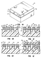
- FIGS. 1A through 1F a first method of constructing a sidewall actuator array 38 for an ink jet printhead in accordance with the teachings of the present invention will now be described in greater detail. More specifically, in FIG. 1A, a generally rectangular block 10 of piezoelectric material may now be seen.
- the block 10 includes a inactive lower body portion 12 formed of an unpoled piezoelectric material or other inactive material such as ceramic, insulatively mounted by a layer of adhesive 14 to an active intermediate body portion 16 formed of an active piezoelectric material poled in the direction of arrow 17.
- the active intermediate body portion 16 is formed using lead zirconate titante (or "PZT").
- inactive lower body portion 12 and the active intermediate body portion 16 will vary depending upon the size of the sidewall actuator array to be manufactured. It is contemplated, however, that the inactive lower body portion 12 and the active intermediate body portion 16 should have similar lengths and widths and that the inactive lower body portion 12 should be at least twice as thick as the active intermediate body portion 16.
- a material removal process is then utilized to form a series of longitudinally extending, substantially parallel grooves 18 in the block 10.
- the grooves 18 are defined by side surfaces 31a, 31b and bottom surface 32, all of which were exposed during the material removal process.
- Each groove 18 extends through the active intermediate body portion 16 and part of the inactive lower body portion 12 and is separated from an adjacent groove 18 by a longitudinally extending sidewall 20 produced during the formation of the grooves 18 and having a top side surface 34.
- Each sidewall 20 is comprised of an inactive lower wall part 22 integrally formed with and originally part of the lower body portion 12 and an active upper wall part 24 originally part of the intermediate body portion 14.
- grooves 18 may extend into the lower body portion 12 a distance generally equal to the thickness of the intermediate body portion 16.
- Grooves 18 may be formed using any of the various machining techniques presently available. For example, a highly precision sawing process would be suitable for forming the grooves 18.
- FIG. 1B it should be clearly understood that the grooves 18 extend from a front end surface 10a to a back end surface 10b of the block 10.
- a layer 26 of conductive material is formed on the top and interior side surfaces 34, 31a of the upper wall parts 24, the interior side surfaces 31b of the lower wall parts 22 and the bottom side surfaces 32 located between the lower wall parts 22.
- the step of forming the conductive layer 26 on the side surfaces 34, 31a, 31b, 32 would be accomplished by depositing a layer of a nichrome-gold alloy on each of the interior side surfaces 31a, 31b, 32 and the top side surfaces 34.
- that portion of the layer 26 of conductive material formed on the top side surfaces 34 of the top wall parts 24 are removed by a conventional demetallization process, for example, using an etching process, after protecting that portion of the layer 26 of conductive material formed on the interior side surfaces 31a, 31b, 32, for example, by masking the aforementioned side surfaces.
- a top body portion 30 formed of an inactive material is mounted to the top side surfaces 34 of the top wall parts 24 by a layer 36 of a non-conductive adhesive material.
- a sidewall actuator array 38 has now been fully assembled.
- the sidewall actuator array 38 is comprised of a series of generally parallel, longitudinally extending channels 40, each of which is defined by a first sidewall actuator 20 (comprised of an inactive lower wall part 22 having an inner side surface 31b and an active upper wall part 24 having an inner side surface 31a), a second sidewall actuator 20 (again comprised of an inactive lower wall part 22 having an inner side surface 31b and an active upper wall part 24 having an inner side surface 31a), a portion of the inactive top body portion 30 separating the first and second sidewall actuators 20 and a portion of the active lower body portion 12 having a bottom side surface 32 separating the first and second sidewall actuators 20.
- each portion 42 of the conductive layer 26 formed along the inner side surfaces 31a, 31b and bottom side surface 32 defining one of the channels 40 is used as an individual contact to be electrically connected to a drive system (not shown) capable of selectively applying a positive or negative voltage to the portion 42.
- the number of channels included sidewall actuator array 38 illustrated in FIG. 1F is purely exemplary and that it is fully contemplated that the sidewall actuator array 38 may include any number of channels. Furthermore, it is recommended that the outermost channel on each side of the sidewall actuator array 38, designated in FIG. 1F as channels 40c and 40d, respectively, should remain inactive. Finally, to complete assembly of an ink jet printhead from the illustrated sidewall actuator array 38, back ends 44 of the channels 40 should be closed and means (not shown) for supplying ink to the channels 40 should be provided.
- sidewall actuator 38' includes a lower body portion 12' formed of an active piezoelectric material poled in a direction opposite to that of the intermediate body portion 14.
- the active lower body portion 12' is provided in place of the inactive lower body portion 12 when forming the block 10.
- the construction of the sidewall actuator array 38' is identical to the technique already described with respect to FIGS. 1A-F.
- a layer 14 of adhesive is used to insulatively mount the active intermediate body portion 16 to the active lower body portion 12'.
- the active lower body portion 12' is poled in direction P1 and the active intermediate body portion 16 is poled in direction P2.
- the series of longitudinally extending, substantially parallel grooves 18 defined by the side surfaces 31a, 31b and bottom surface 32 are then formed.
- each groove 18 extends through the active intermediate body portion 16 and part of the active lower body portion 12' and is separated from an adjacent groove 18 by a longitudinally extending sidewall 20' produced during the formation of the grooves 18.
- Each sidewall 20' thusly formed is comprised of an active lower wall part 22' integrally formed with and originally part of the active lower body portion 12' and an active upper wall part 24 originally part of the intermediate body portion 14.
- the sidewall actuator array 38' thusly constructed is comprised of a series of generally parallel, longitudinally extending channels 40, each of which is defined by a first sidewall actuator 20' (comprised of an active lower wall part 22' having an inner side surface 31b' and an active upper wall part 24 having an inner side surface 31a), a second sidewall actuator 20' (again comprised of an active lower wall part 22 having an inner side surface 31b and an active upper wall part 24 having an inner side surface 31a), a portion of the inactive top body portion 30 separating the first and second sidewall actuators 20' and a portion of the active lower body portion 12' having a bottom side surface 32' separating the first and second sidewall actuators 20'.
- each portion 42 of the conductive layer 26 formed along the inner side surfaces 31a, 31b' and bottom side surface 32' defining one of the channels 40 is used as an individual contact to be electrically connected to a drive system (not shown) capable of selectively applying a positive or negative voltage to the portion 42.
- a drive system capable of selectively applying a positive or negative voltage to the portion 42.
- the application of the electric field E1 causes the sidewall actuator part 22' to deflect into the ink-carrying channel 40b and the application of the electric field E2 causes the sidewall actuator part 24 to also deflect into the ink-carrying channel 40b, thereby imparting a positive pressure pulse into a first ink-carrying channel 40b partially defined thereby and a negative pressure pulse into a second ink-carrying channel 40a partially defined thereby.
- a droplet of ink may be ejected from a front end of the channels.
- sidewall actuator 38'' again includes a lower body portion 12' formed of an active piezoelectric material poled in a direction opposite to that of the intermediate body portion 16. In this embodiment, however, an insulative spacer portion 33 separates the two.
- the active lower body portion 12' is again provided in place of the inactive lower body portion 12 when forming the block 10.
- a layer 15 that portion of which remains after the material removal step being visible in FIG.
- each groove 18 extends through the active intermediate body portion 16, the block of insulative material and part of the active lower body portion 12' and is separated from an adjacent groove 18 by a longitudinally extending sidewall 20'' produced during the formation of the grooves 18.
- Each sidewall 20'' thusly formed is comprised of an active lower wall part 22' integrally formed with and originally part of the active lower body portion 12', an insulative spacer portion 33 and an active upper wall part 24 originally part of the intermediate body portion 14.
- the sidewall actuator array 38'' thusly constructed is comprised of a series of generally parallel, longitudinally extending channels 40, each of which is defined by a first sidewall actuator 20'' (comprised of an active lower wall part 22' having an inner side surface 31b', an insulative spacer part 33 having an inner side surface 33a and an active upper wall part 24 having an inner side surface 31a), a second sidewall actuator 20'' (again comprised of an active lower wall part 22' having an inner side surface 31b', an insulative spacer part 33 having an inner side surface 33a and an active upper wall part 24 having an inner side surface 31a), a portion of the inactive top body portion 30 separating the first and second sidewall actuators 20'' and a portion of the active lower body portion 12' having a bottom side surface 32' separating the first and second sidewall actuators 20''.
- each portion 42 of the conductive layer 26 formed along the inner side surfaces 31a, 33a, 31b' and bottom side surface 32' defining one of the channels 40 is used as an individual contact to be electrically connected to a drive system (not shown) capable of selectively applying a positive or negative voltage to the portion 42.
- a drive system capable of selectively applying a positive or negative voltage to the portion 42.
- the application of the electric field E1 causes the sidewall actuator part 22' to deflect into the ink-carrying channel 40b and the application of the electric field E2 causes the sidewall actuator part 24 to also deflect into the ink-carrying channel 40b, thereby imparting a positive pressure pulse into a first ink-carrying channel 40b partially defined thereby and a negative pressure pulse into a second ink-carrying channel 40a partially defined thereby.
- a droplet of ink may be ejected from a front end of the channels.
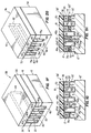
- FIGS. 2A through 2G a second method of constructing a sidewall actuator array for an ink jet printhead in accordance with the teachings of the present invention will now be described in greater detail. More specifically, in FIG. 2A, a generally rectangular block 50 of piezoelectric material, preferably PZT, poled in the direction of arrow 52 may now be seen. Referring next to FIG. 2B, a material removal process is then utilized to form a series of longitudinally extending, substantially parallel grooves 54 which extend partway through the block 50 of poled piezoelectric material. Each of the grooves 54 are separated by an upper wall part 60 from an adjacent groove 54.
- a material removal process is then utilized to form a series of longitudinally extending, substantially parallel grooves 54 which extend partway through the block 50 of poled piezoelectric material. Each of the grooves 54 are separated by an upper wall part 60 from an adjacent groove 54.
- Each upper wall part 60 includes a top side surface 62 and each groove 54 is defined by side and bottom interior side surfaces 56 and 58 of the upper wall part 60 exposed during the material removal process.
- Grooves 54 may be formed using any of the various machining techniques presently available. For example, a highly precision sawing process would be suitable for forming the grooves 54. Furthermore, while not visible in FIG. 2B, it should be clearly understood that the grooves 54 extend from a front end surface 50a to a back end surface 50b of the block 50.
- a layer 64 of conductive material is formed on the top, interior and bottom side surfaces 62, 56, 58 of the upper wall parts 60.
- the step of forming the conductive layer 64 on the side surfaces 62, 56, 58 would be accomplished by depositing a layer of a nichrome-gold alloy on each of the interior side surfaces 56, 58 and the top side surfaces 62. It should be clearly understood, however, that the aforementioned deposition process is but one manner in which a layer of conductive material may be applied to the side surfaces 62, 56, 58 and that numerous other deposition techniques and conductive materials would be suitable to form the layer 64 of conductive material.
- a second material removal step is then performed to extend the grooves 54 downwardly.
- the grooves 54 may be extended using a high precision sawing process. It should be noted, however, that in the second material removal step, the extension of the grooves 54 should be formed slightly narrower than the width of the grooves 54 formed during the first material removal step, thereby preventing the removal of that portion of the layer 64 of conductive material deposited on the side surfaces 56 while removing that portion of the layer 64 deposited on the side surface 58.
- the grooves 54 should be extended such that lower wall parts 66 having interior side surfaces 68 and a height approximately equal to that of the upper wall parts 60 are formed. It should be clearly understood, however, that the height of the lower wall parts 66, relative to the height of the upper wall parts 60 may be varied dramatically without departing from the scope of the invention.
- a top body portion 70 formed of an inactive material is mounted to the top side surfaces 62 of the upper wall parts 60 by a layer 72 of a non-conductive adhesive material.
- a sidewall actuator array 74 has now been fully assembled.
- the sidewall actuator array 74 is comprised of a series of generally parallel, longitudinally extending channels 76, each of which is defined by a first sidewall actuator 78 (comprised of an inactive lower wall part 66 and an active upper wall part 60), a second sidewall actuator 78 (again comprised of an inactive lower wall part 66 and an active upper wall part 60), a portion of the inactive top body portion 70 separating the first and second sidewall actuators 78 and a portion of the unsawed block 50 of active piezoelectric material which separates the first and second sidewall actuators 70.
- first and second inner side surfaces 60 which respectively face first and second channels 76 are a pair of electrical contacts 80-1, 80-2 which are formed by the demetallization of the upper side surface 62 of the active upper wall parts 60.
- the electrical contacts 80-1, 80-2 which face each one of the ink-carrying channels 76 are electrically connected to individual leads of a drive system (not shown) capable of selectively applying a positive or negative voltage to the contacts 80-1, 80-2.
- a droplet of ink may be ejected from a front end of the channels.
- the contacts 80-1 and 80-2 which face a single ink-carrying channel 76 may be electrically connected to a single lead of the drive system.
- a positive voltage would be applied to the electrical contact 80-1 and 80-2 facing the channel 76 while a negative voltage is applied to the electrical contacts 80-2, 80-1 on the opposite sides of the sidewall actuators 78 facing the selected channel 76.
- the number of channels 76 included in the sidewall actuator array 74 illustrated in FIG. 2F is purely exemplary and that it is fully contemplated that the sidewall actuator array 74 may include any number of channels. Furthermore, it is recommended that the outermost channel on each side of the sidewall actuator array 74, designated in FIG. 2G as channels 76c and 76d, respectively, should remain inactive. Finally, to complete assembly of an ink jet printhead from the illustrated sidewall actuator array 74, back ends 82 of the channels 76 should be closed and means (not shown) for supplying ink to the channels 76 should be provided.
Abstract
Description
- The present invention relates to a method for manufacturing a sidewall actuator array for an ink jet printhead and, more particularly, to a method for manufacturing a sidewall actuator array for an ink jet printhead using a single or double groove forming step orientated in the poling direction for the sidewall actuators.
- Printers provide a means of outputting a permanent record in human readable form. Typically, a printing technique may be categorized as either impact printing or non-impact printing. In impact printing, an image is formed by striking an inked ribbon placed near the surface of the paper. Impact printing techniques may be further characterized as either formed-character printing or matrix printing. In formed-character printing, the element which strikes the ribbon to produce the image consists of a raised mirror image of the desired character. In matrix printing, the character is formed as a series of closely spaced dots which are produced by striking a provided wire or wires against the ribbon. Here, characters are formed as a series of closely spaced dots produced by striking the provided wire or wires against the ribbon. By selectively striking the provided wires, any character representable by a matrix of dots can be produced.
- Non-impact printing is often preferred over impact printing in view of its tendency to provide higher printing speeds as well as its better suitability for printing graphics and half-tone images. Non-impact printing techniques include matrix, electrostatic and electrophotographic type printing techniques. In matrix type printing, wires are selectively heated by electrical pulses and the heat thereby generated causes a mark to appear on a sheet of paper, usually specially treated paper. In electrostatic type printing, an electric arc between the printing element and the conductive paper removes an opaque coating on the paper to expose a sublayer of a contrasting color. Finally, in electrophotographic printing, a photoconductive material is selectively charged utilizing a light source such as a laser. A powder toner is attracted to the charged regions and, when placed in contact with a sheet of paper, transfers to the paper's surface. The toner is then subjected to heat which fuses it to the paper.
- Another form of non-impact printing is generally classified as ink jet printing. Ink jet printing systems use the ejection of tiny droplets of ink to produce an image. The devices produce highly reproducible and controllable droplets so that a droplet may be printed at a location specified by digitally stored image data. Most ink jet printing systems commercially available may be generally classified as either a "continuous jet" type ink jet printing system where droplets are continuously ejected from the printhead and either directed to or away from the paper depending on the desired image to be produced or as a "drop-on-demand" type ink jet printing system where droplets are ejected from the printhead in response to a specific command related to the image to be produced.
- In a continuous jet type ink jet printer, a pump supplies ink to a nozzle assembly where the pumping pressure forces the ink to be ejected therefrom in a continuous stream. The nozzle assembly includes a piezo crystal continuously driven by an electrical voltage, thereby creating pressure disturbances that cause the continuous stream of ink ejected therefrom to break up into uniform droplets of ink. The droplets acquire an electrostatic charge due to the presence of an electrostatic field established close to the ejection orifice. Using high voltage deflection plates, the trajectory of selected ones of the electrostatically charged droplets can be controlled to hit a desired spot on a sheet of paper. The high voltage deflection plates can also deflect unselected ones of the electrostatically charged droplets away from the sheet of paper and into a reservoir for recycling purposes. Due to the small size of the droplets and the precise trajectory control, the quality of continuous jet type ink jet printing systems can approach that of formed-character impact printing systems. However, one drawback to continuous jet type ink jet printing systems is that fluid must be jetting even when little or no printing is required. This requirement degrades the ink and decreases reliability of the printing system.
- Due to this drawback, there has been increased interest in those printing systems in which droplets are ejected from the printhead by electromechanically induced pressure waves. In this type of printing system, a volumetric change in the fluid is induced by the application of a voltage pulse to a piezoelectric material which is directly or indirectly coupled to the fluid. This volumetric change causes pressure/velocity transients to occur in the fluid, thereby causing the ejection of a droplet therefrom. Since the voltage is applied only when a droplet is desired, these types of ink jet printing systems are referred to as "drop-on-demand" type ink jet printing systems.
- A typical drop-on-demand type ink jet printing system is disclosed in U.S. Patent No. 3,946,398 to Kyser et al. In Kyser et al., a pressure plate formed from two transversely expandable piezoelectric plates is utilized as the upper wall of an ink-carrying pressure chamber. By applying a voltage across the piezoelectric plates, the pressure plate flexes inwardly into the pressure chamber, thereby causing a fluid displacing volumetric change within the chamber. Another typical drop-on-demand type ink jet printing system may be seen by reference to U.S. Patent No. 3,857,045 to Zoltan. In Zoltan, a tubular piezoelectric transducer surrounds an ink-carrying channel. When the transducer is excited by the application of an electrical voltage pulse, the ink-carrying channel is compressed and a drop of ink is ejected from the channel. However, the relatively low channel density achieved by such systems as well as the relatively complicated arrangement of the piezoelectric transducer and the associated ink-carrying channel which characterizes such systems causes such systems to be time-consuming and expensive to manufacture.
- In order to reduce the per ink-carrying channel (or "jet") manufacturing cost of an ink jet printhead, in particular, those ink jet printheads having a piezoelectric actuator, it has long been desired to produce an ink jet printhead having a channel array in which the individual channels which comprise the array are arranged such that the spacing between adjacent channels is relatively small. For example, it would be very desirable to construct an ink jet printhead having a channel array where adjacent channels are spaced between approximately four and eight mils apart. Such a ink jet printhead is hereby defined as a "high density" ink jet printhead. In addition to a reduction in the per ink-carrying channel manufacturing cost, another advantage which would result from the manufacture of an ink jet printhead with a high channel density would be an increase in printer speed. However, the very close spacing between channels in the proposed high density ink jet printhead has long been a major problem in the manufacture of such printheads.
- Many attempts to manufacture ink jet printheads having piezoelectric actuators and reduced spacing between channels have focussed on the manufacture of ink jet printheads with parallel channel arrays and shear mode piezoelectric transducers for actuating the channels. For example, U.S. Patent Nos. 4,584,590 and 4,825,227, both to Fischbeck et al., disclose shear mode piezoelectric transducers for a parallel channel array ink jet printhead. In both of the Fischbeck et al. patents, a series of open ended parallel ink pressure chambers are covered with a sheet of a piezoelectric material along their roofs. Electrodes are provided on opposite sides of the sheet of piezoelectric material such that positive electrodes are positioned above the vertical walls separating pressure chambers and negative electrodes are positioned over the chamber itself. When an electric field is provided across the electrodes, the piezoelectric material, which is polled in a direction normal to the electric field direction, distorts in a shear mode configuration to compress the ink pressure chamber. In these configurations, however, much of the piezoelectric material is inactive. Furthermore, the extent of deformation of the piezoelectric element tends to be small, thereby minimizing the pressure pulse which may be applied to the ink by the actuator.
- An ink jet printhead having a parallel channel array and which utilizes piezoelectric materials to construct the sidewalls of the ink-carrying channels may be seen by reference to U.S. Patent No. 4,536,097 to Nilsson. In Nilsson, an ink jet channel matrix is formed by a series of strips of a piezoelectric material disposed in spaced parallel relationships and covered on opposite sides by first and second plates. One plate is constructed of a conductive material and forms a shared electrode for all of the strips of piezoelectric material. On the other side of the strips, electrical contacts are used to electrically connect channel defining pairs of the strips of piezoelectric material. When a voltage is applied to the two strips of piezoelectric material which define a channel, the strips become narrower and higher such that the enclosed cross-sectional area of the channel is enlarged and ink is drawn into the channel. When the voltage is removed, the strips return to their original shape, thereby reducing channel volume and ejecting ink therefrom.
- An ink jet printhead having a parallel ink-carrying channel array and which utilizes piezoelectric material to form a shear mode actuator for the vertical walls of the channel has also been disclosed. For example, U.S. Patent Nos. 4,879,568 to Bartky et al. and 4,887,100 to Michaelis et al. each disclose an ink jet printhead channel array in which a piezoelectric material is used as the vertical wall along the entire length of each channel forming the array. In these configurations, the vertical channel walls are constructed of two oppositely polled pieces of piezoelectric material mounted next to each other and sandwiched between top and bottom walls to form the ink channels. Electrodes are formed along the entire height of the vertical channel walls. When an electric field normal to the polling direction of the pieces of piezoelectric material is generated between a pair of electrodes formed on opposite sides of a vertical wall, both of the oppositely poled pieces of piezoelectric material distort in a first direction to compress the ink channel.
- The process by which the electrodes are formed in Bartky et al. and Michaelis et al. for the above-referenced piezoelectric sidewall actuator configurations is simplified by the fact that active material is utilized for the entire height of the sidewalls. Where the entire sidewall is not formed of active material or should not have an electrode deposited thereon, Bartky et al., Michaelis et al. and, with even greater particularity, U.S Patent No. 5,016,028 to Temple, the recommended process by which electrodes are to be formed along the sidewalls becomes even more complicated. In such configurations, it is recommended that the channel array should be orientated to the electrode depositing, metal vapor beam such that electrode deposition will only take place along part of each sidewall.
- It can be readily seen from the foregoing that it would be desirable to provide improved methods for manufacturing sidewall actuator arrays for ink jet printheads which eliminates, or at least substantially reduces, many of the above-mentioned limitations and disadvantages associated with prior methods for manufacturing channel arrays having partially or fully active sidewall actuators. It is, therefore, an object of the present invention to provide such improved methods of manufacturing ink jet printheads.
- In one embodiment, the present invention is of a method of manufacturing, for an ink jet printhead, a sidewall actuator array comprised of a series of sidewall actuators, each having a first part formed from an active material and a second part formed from an inactive material. A lower body portion formed of an inactive material, an intermediate body portion formed of an active material and an upper body portion formed of an inactive material are first provided. The active intermediate body portion includes top and bottom side surfaces and is poled in a first direction generally normal to the top and bottom side surfaces thereof. To construct the sidewall actuator array, the bottom side surface of the active intermediate body portion is mounted to a top side surface of the inactive lower body portion and interior side surfaces of the active intermediate and inactive lower body portions are exposed by forming a series of generally parallel, longitudinally extending grooves which extend through the active intermediate body portion and part of the inactive lower body portion, for example, using a sawing process. A layer of conductive material is deposited on the interior side surfaces of the active intermediate and inactive lower body portions. The bottom side surface of the inactive upper body portion is then insulatively mounted to the top side surface of the active intermediate body portion to form the sidewall actuator array.
- In one aspect thereof, the grooves are formed such that they extend into the inactive lower body portion a distance generally equal to the height of the active intermediate body portion. In another aspect thereof, the grooves are formed by removing selected parts of the active intermediate body portion and the inactive lower body portion to form a series of generally parallel, longitudinally extending sidewall actuators, each having an inactive lower wall part having first and second interior side surfaces, an active upper wall part having first and second interior side surfaces and a top side surface. Each of the sidewall actuators formed in this manner are separated from an adjacent sidewall actuator by an interior side surface of the inactive lower body portion which is exposed during the removal of the selected part of the inactive lower body portion. In a further aspect thereof, the layer of conductive material is deposited on the interior surfaces of the active intermediate and inactive lower body portions by metallizing the top side surface of the active upper wall part and the interior side surfaces of the active upper and inactive lower wall parts. The top side surface of the active upper wall part is then demetallized. In yet another aspect thereof, an interior side surface of the lower body portion is also metallized.
- In an alternate embodiment thereof, the present invention is of a method of manufacturing, for an ink jet printhead, a sidewall actuator array comprised of a series of sidewall actuators, each having first and second parts formed from respective pieces of active material poled in opposite directions. This method of manufacture differs from the above-described embodiment of the invention in that a lower body portion formed of an active material is provided in place of the inactive material previously utilized. To construct the sidewall actuator array, a bottom side surface of the active intermediate body portion is mounted to a top side surface of the active lower body portion such that the lower body portion is poled in a first direction normal to the top side surface thereof and the intermediate body portion is poled in a second direction normal to the bottom side surface thereof and opposite to the first direction. After completing manufacture in accordance with the above-described method of the invention, a sidewall actuator array comprised of a series of sidewalls, each having an active lower sidewall part poled in a first direction and an active upper sidewall part poled in a second direction opposite to the first direction, is produced.
- In a variant of this alternate embodiment of the invention, a block of insulative material is utilized to form a series of spacers for separating the lower and active upper sidewall parts of each sidewall. A bottom side surface of the block of insulative material is mounted to the top side surface of the active lower body portion, which, as before, is poled in a first direction normal to the top side surface thereof. A bottom side surface of the active intermediate body portion is then mounted to a top side surface of the insulative spacing material. A series of generally parallel, longitudinally extending grooves which extend through the intermediate body portion, the spacing material and part of the lower body portion are then formed. After completing manufacture in accordance with the above-described method of the invention, a sidewall actuator array comprised of a series of sidewalls, each comprised of upper and lower active sidewall parts poled in opposite directions and separated by an insulative spacer, is produced.
- In another embodiment, the present invention is of a method of manufacturing, for an ink jet printhead, a sidewall actuator array comprised of a series of sidewall actuators. A lower body portion having top and bottom side surfaces thereof and formed of an active piezoelectric material poled in a first direction generally orthogonal to the top and bottom side surfaces is provided. A series of generally parallel, longitudinally extending grooves which extend into the lower body portion a specified distance from the top side surface are then formed. The aforementioned grooves are defined by first interior side surfaces of the lower body portion exposed during the forming step. A layer of conductive material is deposited on the first interior side surfaces of the lower body portion. The grooves formed in the lower body portion are then deepened to expose second interior side surfaces of the lower body portion. A bottom side surface of the inactive upper body portion is then mounted to the top side surface of the active intermediate body portion to form the sidewall actuator array. In one aspect thereof, the layer of conductive material is deposited on the interior side surface of the lower body portion by depositing a layer of conductive material on the top and interior side surfaces of the upper wall parts followed by removing the portion of the layer of conductive material which was deposited on the top side surfaces of the upper wall part.
- The present invention may be better understood, and its numerous objects, features and advantages will become apparent to those skilled in the art by reference to the accompanying drawing, in which:
- FIG. 1A is a perspective view of a block of piezoelectric material suitable for use in manufacturing a sidewall actuator array for an ink jet printhead in accordance with the teachings of the present invention;
- FIG. 1B is an enlarged partial cross-sectional view taken along
line 1B--1B of FIG. 1A after a forming step has formed a series of grooves therein; - FIG. 1C is an enlarged partial cross-sectional view of the grooved block of FIG. 1B after a metallization step;
- FIG. 1D is an enlarged partial cross-sectional view of the metallized grooved block of FIG. 1C after a partial demetallization step;
- FIG. 1E is an enlarged partial cross-sectional view of the partially demetallized grooved block of FIG. 1D after a cover has been mounted thereto to complete assembly of a sidewall actuator array for an ink jet printhead;
- FIG. 1F is a perspective view of the fully assembled sidewall actuator array for an ink jet printhead of FIG. 1E;
- FIG. 1G is an enlarged partial cross-sectional view of an alternate configuration of the sidewall actuator array for an ink jet printhead of FIG. 1E in which an active lower body portion has been substituted for the inactive lower body portion prior to the formation of a series of grooves therein;
- FIG. 1H is an enlarged partial cross-sectional view of a variant of the sidewall actuator array for an ink jet printhead of FIG. 1G in which an insulative spacer is mounted to the active lower body portion prior to the mounting of the active intermediate body portion thereto;
- FIG. 2A is a perspective view of a block of poled piezoelectric material suitable for use in manufacturing a sidewall actuator array for an ink jet printhead in accordance with the teachings of the present invention;
- FIG. 2B is an enlarged partial cross-sectional view taken along
line 2B--2B of FIG. 2A after a first forming step has formed a series of grooves therein; - FIG. 2C is an enlarged partial cross-sectional view of the grooved block of FIG. 2B after a metallization step;
- FIG. 2D is an enlarged partial cross-sectional view of the metallized grooved block of FIG. 2C after a second forming step has deepened the previously formed series of grooves;
- FIG. 2E is an enlarged partial cross-sectional view of the metallized grooved block of FIG. 2D after a partial demetallization step;
- FIG. 2F is an enlarged partial cross-sectional view of the partially demetallized grooved block of FIG. 2E after a cover has been mounted thereto to complete assembly of a sidewall actuator array for an ink jet printhead; and
- FIG. 2G is a perspective view of the fully assembled sidewall actuator array for an ink jet printhead of FIG. 2F.
- Referring now to FIGS. 1A through 1F, a first method of constructing a
sidewall actuator array 38 for an ink jet printhead in accordance with the teachings of the present invention will now be described in greater detail. More specifically, in FIG. 1A, a generally rectangular block 10 of piezoelectric material may now be seen. The block 10 includes a inactivelower body portion 12 formed of an unpoled piezoelectric material or other inactive material such as ceramic, insulatively mounted by a layer of adhesive 14 to an activeintermediate body portion 16 formed of an active piezoelectric material poled in the direction ofarrow 17. Preferably, the activeintermediate body portion 16 is formed using lead zirconate titante (or "PZT"). It should be clearly understood, however, that other active piezoelectric material would be suitable for use herein without departing from the scope of the invention. The exact length, width and height of the inactivelower body portion 12 and the activeintermediate body portion 16 will vary depending upon the size of the sidewall actuator array to be manufactured. It is contemplated, however, that the inactivelower body portion 12 and the activeintermediate body portion 16 should have similar lengths and widths and that the inactivelower body portion 12 should be at least twice as thick as the activeintermediate body portion 16. - Referring next to FIG. 1B, a material removal process is then utilized to form a series of longitudinally extending, substantially
parallel grooves 18 in the block 10. Thegrooves 18 are defined byside surfaces bottom surface 32, all of which were exposed during the material removal process. Eachgroove 18 extends through the activeintermediate body portion 16 and part of the inactivelower body portion 12 and is separated from anadjacent groove 18 by alongitudinally extending sidewall 20 produced during the formation of thegrooves 18 and having atop side surface 34. Eachsidewall 20 is comprised of an inactivelower wall part 22 integrally formed with and originally part of thelower body portion 12 and an activeupper wall part 24 originally part of theintermediate body portion 14. While the extent to which thegrooves 18 may extend into thelower body portion 12 may be varied without departing from the scope of the present invention, it is contemplated that thegrooves 18 should be formed such that extend into the lower body portion 12 a distance generally equal to the thickness of theintermediate body portion 16.Grooves 18 may be formed using any of the various machining techniques presently available. For example, a highly precision sawing process would be suitable for forming thegrooves 18. Furthermore, while not visible in FIG. 1B, it should be clearly understood that thegrooves 18 extend from afront end surface 10a to aback end surface 10b of the block 10. - Referring next to FIG. 1C, a
layer 26 of conductive material is formed on the top and interior side surfaces 34, 31a of theupper wall parts 24, the interior side surfaces 31b of thelower wall parts 22 and the bottom side surfaces 32 located between thelower wall parts 22. Preferably, the step of forming theconductive layer 26 on the side surfaces 34, 31a, 31b, 32 would be accomplished by depositing a layer of a nichrome-gold alloy on each of the interior side surfaces 31a, 31b, 32 and the top side surfaces 34. It should be clearly understood, however, that the aforementioned deposition process is but one manner in which a layer of conductive material may be applied to thesurfaces - Referring next to FIG. 1D, that portion of the
layer 26 of conductive material formed on the top side surfaces 34 of thetop wall parts 24 are removed by a conventional demetallization process, for example, using an etching process, after protecting that portion of thelayer 26 of conductive material formed on the interior side surfaces 31a, 31b, 32, for example, by masking the aforementioned side surfaces. - Referring next to FIG. 1E, a
top body portion 30 formed of an inactive material is mounted to the top side surfaces 34 of thetop wall parts 24 by alayer 36 of a non-conductive adhesive material. As may now be seen in FIG. 1E, as well as FIG. 1F, asidewall actuator array 38 has now been fully assembled. Thesidewall actuator array 38 is comprised of a series of generally parallel, longitudinally extendingchannels 40, each of which is defined by a first sidewall actuator 20 (comprised of an inactivelower wall part 22 having aninner side surface 31b and an activeupper wall part 24 having aninner side surface 31a), a second sidewall actuator 20 (again comprised of an inactivelower wall part 22 having aninner side surface 31b and an activeupper wall part 24 having aninner side surface 31a), a portion of the inactivetop body portion 30 separating the first andsecond sidewall actuators 20 and a portion of the activelower body portion 12 having abottom side surface 32 separating the first andsecond sidewall actuators 20. - To electrically connect the
sidewall actuator array 38, eachportion 42 of theconductive layer 26 formed along theinner side surfaces bottom side surface 32 defining one of thechannels 40 is used as an individual contact to be electrically connected to a drive system (not shown) capable of selectively applying a positive or negative voltage to theportion 42. When a positive voltage is applied to afirst contact 42a and a negative voltage is applied to asecond contact 42b, an electric field E normal to the poling direction P is produced across the sidewall actuator 20a, thereby causing the sidewall actuator 20a to deflect into the ink-carryingchannel 40b, thereby imparting a positive pressure pulse into a first ink-carryingchannel 40b partially defined thereby and a negative pressure pulse into a second ink-carrying channel 40a partially defined thereby. By proper application of positive and/or negative pressure pulses to the ink-carryingchannels 40, a droplet of ink may be ejected from a front end of the channels. - It should be clearly noted, however, that the number of channels included
sidewall actuator array 38 illustrated in FIG. 1F is purely exemplary and that it is fully contemplated that thesidewall actuator array 38 may include any number of channels. Furthermore, it is recommended that the outermost channel on each side of thesidewall actuator array 38, designated in FIG. 1F as channels 40c and 40d, respectively, should remain inactive. Finally, to complete assembly of an ink jet printhead from the illustratedsidewall actuator array 38, back ends 44 of thechannels 40 should be closed and means (not shown) for supplying ink to thechannels 40 should be provided. - Referring next to FIG. 1G, an alternate configuration of the
sidewall actuator array 38 of FIG. 1E will now be described in greater detail. In this embodiment of the invention, sidewall actuator 38' includes alower body portion 12' formed of an active piezoelectric material poled in a direction opposite to that of theintermediate body portion 14. To construct the sidewall actuator array 38', the activelower body portion 12' is provided in place of the inactivelower body portion 12 when forming the block 10. Apart from this substitution of material, the construction of the sidewall actuator array 38' is identical to the technique already described with respect to FIGS. 1A-F. Thus, as before, alayer 14 of adhesive is used to insulatively mount the activeintermediate body portion 16 to the activelower body portion 12'. The activelower body portion 12' is poled in direction P1 and the activeintermediate body portion 16 is poled in direction P2. The series of longitudinally extending, substantiallyparallel grooves 18 defined by the side surfaces 31a, 31b andbottom surface 32 are then formed. In this embodiment, however, eachgroove 18 extends through the activeintermediate body portion 16 and part of the activelower body portion 12' and is separated from anadjacent groove 18 by a longitudinally extending sidewall 20' produced during the formation of thegrooves 18. Each sidewall 20' thusly formed is comprised of an active lower wall part 22' integrally formed with and originally part of the activelower body portion 12' and an activeupper wall part 24 originally part of theintermediate body portion 14. - After completing construction in the afore-described manner, the sidewall actuator array 38' thusly constructed is comprised of a series of generally parallel, longitudinally extending
channels 40, each of which is defined by a first sidewall actuator 20' (comprised of an active lower wall part 22' having aninner side surface 31b' and an activeupper wall part 24 having aninner side surface 31a), a second sidewall actuator 20' (again comprised of an activelower wall part 22 having aninner side surface 31b and an activeupper wall part 24 having aninner side surface 31a), a portion of the inactivetop body portion 30 separating the first and second sidewall actuators 20' and a portion of the activelower body portion 12' having a bottom side surface 32' separating the first and second sidewall actuators 20'. - Once the sidewall actuator array 38' is electrically connected in the manner previously described, each
portion 42 of theconductive layer 26 formed along theinner side surfaces channels 40 is used as an individual contact to be electrically connected to a drive system (not shown) capable of selectively applying a positive or negative voltage to theportion 42. When a positive voltage is applied to afirst contact 42a and a negative voltage is applied to asecond contact 42b, electric fields E1 and E2, each of which is normal to the poling direction P1 and P2, respectively, of thesidewall actuator parts 22' and 24. The application of the electric field E1 causes the sidewall actuator part 22' to deflect into the ink-carryingchannel 40b and the application of the electric field E2 causes thesidewall actuator part 24 to also deflect into the ink-carryingchannel 40b, thereby imparting a positive pressure pulse into a first ink-carryingchannel 40b partially defined thereby and a negative pressure pulse into a second ink-carrying channel 40a partially defined thereby. By proper application of positive and/or negative pressure pulses to the ink-carryingchannels 40, a droplet of ink may be ejected from a front end of the channels. - Referring next to FIG. 1H, a variant of the sidewall actuator array 38' of FIG. 1G will now be described in greater detail. In this embodiment of the invention, sidewall actuator 38'' again includes a
lower body portion 12' formed of an active piezoelectric material poled in a direction opposite to that of theintermediate body portion 16. In this embodiment, however, aninsulative spacer portion 33 separates the two. To construct the sidewall actuator array 38'', the activelower body portion 12' is again provided in place of the inactivelower body portion 12 when forming the block 10. A layer 15 (that portion of which remains after the material removal step being visible in FIG. 1H) ofadhesive 15 is then used to insulatively mount a bottom side surface of a block of insulative material to a top side surface of the activelower body portion 12'. Next, a layer 14' (again, that portion of which remains after the material removal step being visible in FIG. 1H) of adhesive is used to insulatively mount a bottom side surface of the activeintermediate body portion 16 to a top side surface of the block of insulative material. The series of longitudinally extending, substantiallyparallel grooves 18 defined by the side surfaces 31a, 33a, 31b' and bottom surface 32' are then formed. In this embodiment, however, eachgroove 18 extends through the activeintermediate body portion 16, the block of insulative material and part of the activelower body portion 12' and is separated from anadjacent groove 18 by a longitudinally extending sidewall 20'' produced during the formation of thegrooves 18. Each sidewall 20'' thusly formed is comprised of an active lower wall part 22' integrally formed with and originally part of the activelower body portion 12', aninsulative spacer portion 33 and an activeupper wall part 24 originally part of theintermediate body portion 14. - After completing construction of the sidewall actuator array 38'' in the afore-described manner, the sidewall actuator array 38'' thusly constructed is comprised of a series of generally parallel, longitudinally extending
channels 40, each of which is defined by a first sidewall actuator 20'' (comprised of an active lower wall part 22' having aninner side surface 31b', aninsulative spacer part 33 having an inner side surface 33a and an activeupper wall part 24 having aninner side surface 31a), a second sidewall actuator 20'' (again comprised of an active lower wall part 22' having aninner side surface 31b', aninsulative spacer part 33 having an inner side surface 33a and an activeupper wall part 24 having aninner side surface 31a), a portion of the inactivetop body portion 30 separating the first and second sidewall actuators 20'' and a portion of the activelower body portion 12' having a bottom side surface 32' separating the first and second sidewall actuators 20''. - Once the sidewall actuator array 38'' is electrically connected in the manner previously described, each
portion 42 of theconductive layer 26 formed along theinner side surfaces channels 40 is used as an individual contact to be electrically connected to a drive system (not shown) capable of selectively applying a positive or negative voltage to theportion 42. When a positive voltage is applied to afirst contact 42a and a negative voltage is applied to asecond contact 42b, electric fields E1 and E2, each of which is normal to the poling direction P1 and P2, respectively, of thesidewall actuator parts 22' and 24. The application of the electric field E1 causes the sidewall actuator part 22' to deflect into the ink-carryingchannel 40b and the application of the electric field E2 causes thesidewall actuator part 24 to also deflect into the ink-carryingchannel 40b, thereby imparting a positive pressure pulse into a first ink-carryingchannel 40b partially defined thereby and a negative pressure pulse into a second ink-carrying channel 40a partially defined thereby. By proper application of positive and/or negative pressure pulses to the ink-carryingchannels 40, a droplet of ink may be ejected from a front end of the channels. - Referring next to FIGS. 2A through 2G, a second method of constructing a sidewall actuator array for an ink jet printhead in accordance with the teachings of the present invention will now be described in greater detail. More specifically, in FIG. 2A, a generally
rectangular block 50 of piezoelectric material, preferably PZT, poled in the direction ofarrow 52 may now be seen. Referring next to FIG. 2B, a material removal process is then utilized to form a series of longitudinally extending, substantiallyparallel grooves 54 which extend partway through theblock 50 of poled piezoelectric material. Each of thegrooves 54 are separated by anupper wall part 60 from anadjacent groove 54. Eachupper wall part 60 includes atop side surface 62 and eachgroove 54 is defined by side and bottom interior side surfaces 56 and 58 of theupper wall part 60 exposed during the material removal process.Grooves 54 may be formed using any of the various machining techniques presently available. For example, a highly precision sawing process would be suitable for forming thegrooves 54. Furthermore, while not visible in FIG. 2B, it should be clearly understood that thegrooves 54 extend from afront end surface 50a to aback end surface 50b of theblock 50. - Referring next to FIG. 2C, a
layer 64 of conductive material is formed on the top, interior and bottom side surfaces 62, 56, 58 of theupper wall parts 60. Preferably, the step of forming theconductive layer 64 on the side surfaces 62, 56, 58 would be accomplished by depositing a layer of a nichrome-gold alloy on each of the interior side surfaces 56, 58 and the top side surfaces 62. It should be clearly understood, however, that the aforementioned deposition process is but one manner in which a layer of conductive material may be applied to the side surfaces 62, 56, 58 and that numerous other deposition techniques and conductive materials would be suitable to form thelayer 64 of conductive material. - Referring next to FIG. 2D, a second material removal step is then performed to extend the
grooves 54 downwardly. As before, thegrooves 54 may be extended using a high precision sawing process. It should be noted, however, that in the second material removal step, the extension of thegrooves 54 should be formed slightly narrower than the width of thegrooves 54 formed during the first material removal step, thereby preventing the removal of that portion of thelayer 64 of conductive material deposited on the side surfaces 56 while removing that portion of thelayer 64 deposited on theside surface 58. Preferably, thegrooves 54 should be extended such thatlower wall parts 66 having interior side surfaces 68 and a height approximately equal to that of theupper wall parts 60 are formed. It should be clearly understood, however, that the height of thelower wall parts 66, relative to the height of theupper wall parts 60 may be varied dramatically without departing from the scope of the invention. - Referring next to FIG. 2E, that portion of the
layer 64 of conductive material formed on the top side surfaces 62 of theupper wall parts 58 are removed by a conventional demetallization process, for example, using an etching process after masking that portion of thelayer 64 of conductive material deposited on the side surfaces 56. Finally, as illustrated in FIG. 2F, atop body portion 70 formed of an inactive material is mounted to the top side surfaces 62 of theupper wall parts 60 by alayer 72 of a non-conductive adhesive material. As may now be seen in FIG. 2F, as well as FIG. 2G, asidewall actuator array 74 has now been fully assembled. Thesidewall actuator array 74 is comprised of a series of generally parallel, longitudinally extendingchannels 76, each of which is defined by a first sidewall actuator 78 (comprised of an inactivelower wall part 66 and an active upper wall part 60), a second sidewall actuator 78 (again comprised of an inactivelower wall part 66 and an active upper wall part 60), a portion of the inactivetop body portion 70 separating the first andsecond sidewall actuators 78 and a portion of theunsawed block 50 of active piezoelectric material which separates the first andsecond sidewall actuators 70. Provided on first and second inner side surfaces 60 which respectively face first andsecond channels 76 are a pair of electrical contacts 80-1, 80-2 which are formed by the demetallization of theupper side surface 62 of the activeupper wall parts 60. - To electrically connect the
sidewall actuator array 78, the electrical contacts 80-1, 80-2 which face each one of the ink-carryingchannels 76 are electrically connected to individual leads of a drive system (not shown) capable of selectively applying a positive or negative voltage to the contacts 80-1, 80-2. When a positive voltage is applied to a contact 80-2 on one side of a selected sidewall actuator and a negative voltage is applied to a contact 80-1 on the other side of the selected sidewall actuator, an electric field E normal to the poling direction P is produced across the upper wall part of the selected sidewall actuator, thereby causing the sidewall actuator to deflect into the ink-carryingchannel 76, thereby imparting a positive pressure pulse into a first ink-carryingchannel 76b partially defined thereby and a negative pressure pulse into a second ink-carryingchannel 76a partially defined thereby. By proper application of positive and/or negative pressure pulses to the ink-carryingchannels 76, a droplet of ink may be ejected from a front end of the channels. It is further contemplated that, in one aspect of the invention, the contacts 80-1 and 80-2 which face a single ink-carryingchannel 76 may be electrically connected to a single lead of the drive system. In this aspect, to drive both of thesidewall actuators 78 into a selectedchannel 76, a positive voltage would be applied to the electrical contact 80-1 and 80-2 facing thechannel 76 while a negative voltage is applied to the electrical contacts 80-2, 80-1 on the opposite sides of thesidewall actuators 78 facing the selectedchannel 76. - As before, it should be clearly noted, however, that the number of
channels 76 included in thesidewall actuator array 74 illustrated in FIG. 2F is purely exemplary and that it is fully contemplated that thesidewall actuator array 74 may include any number of channels. Furthermore, it is recommended that the outermost channel on each side of thesidewall actuator array 74, designated in FIG. 2G aschannels sidewall actuator array 74, back ends 82 of thechannels 76 should be closed and means (not shown) for supplying ink to thechannels 76 should be provided. - Thus, there has been described an illustrated herein, various methods for manufacturing a sidewall actuator array for an ink jet printhead. Each of the disclosed methods provide a relatively simple and inexpensive method of manufacturing the aforementioned arrays which simplifies those methods taught by the prior art. Rather than requiring the precise deposition of conductive material at specific locations along an interior sidewall, the provision of a single metallization step between two material removal steps form the desired sidewall actuators without the need for a precise deposition step. However, those skilled in the art will recognize that many modifications and variations besides those specifically mentioned may be made in the techniques described herein without departing substantially from the concept of the present invention. Accordingly, it should be clearly understood that the form of the invention as described herein is exemplary only and is not intended as a limitation on the scope of the invention.
Claims (21)
- A method of manufacturing a sidewall actuator array for an ink jet printhead, said sidewall actuator array comprised of a series of sidewall actuators, each having a first part formed from an active material and a second part formed from an inactive material, comprising the steps of:
providing a lower body portion formed of an inactive material and having a top side surface, an intermediate body portion having bottom and top side surfaces and formed of an active piezoelectric material poled in a direction generally normal to said bottom and top side surfaces, and an upper body portion formed of an inactive material and having a bottom side surface;
mounting said bottom side surface of said active intermediate body portion to said top side surface of said inactive lower body portion;
forming a series of generally parallel, longitudinally extending grooves which extend through said active intermediate body portion and part of said inactive lower body portion, said grooves being formed generally parallel with said poling direction of said active intermediate body portion and exposing interior side surfaces of said active intermediate body portion and said inactive lower body portion;
depositing a layer of conductive material on said interior side surfaces of said active intermediate body portion and said inactive lower body portion; and
insulatively mounting said bottom side surface of said inactive upper body portion to said top side surface of said active intermediate body portion to form said sidewall actuator array. - A method of manufacturing a sidewall actuator array for an ink jet printhead according to claim 1 wherein said grooves are formed such that they extend into said inactive lower body portion a distance generally equal to the height of said active intermediate body portion.
- A method of manufacturing a sidewall actuator array for an ink jet printhead according to claim 1 and further comprising the step of sawing a series of generally parallel, longitudinally extending grooves which extend through said active intermediate body portion and part of said inactive lower body portion.
- A method of manufacturing a sidewall actuator array for an ink jet printhead according to claim 1 wherein the step of forming a series of generally parallel, longitudinally extending grooves further comprises the step of removing selected parts of said active intermediate body portion and said inactive lower body portion to form a series of generally parallel, longitudinally extending sidewall actuators, each said sidewall actuator having an inactive lower wall part having first and second interior side surfaces, an active upper wall part having first and second interior side surfaces and a top side surface, each of said sidewall actuators being separated from an adjacent sidewall actuator by an interior side surface of said inactive lower body portion which is exposed during the removal of said selected part of said inactive lower body portion.
- A method of manufacturing a sidewall actuator array for an ink jet printhead according to claim 1 wherein the step of depositing a layer of conductive material on said interior surfaces of said active intermediate body portion and said inactive lower body portion further comprises the steps of:
metallizing said top side surface of said active upper wall part and said interior side surfaces of said active upper wall part and said inactive lower wall part; and
demetallizing said top side surface of said active upper wall part. - A method of manufacturing a sidewall actuator array for an ink jet printhead according to claim 5 wherein the step of metallizing said interior side surfaces of said active upper wall part and said inactive lower wall part further comprises the step of metallizing said interior side surface of said lower body portion.
- A method of manufacturing a sidewall actuator array for an ink jet printhead according to claim 6 wherein said upper and lower sidewall parts are formed such that the height of said lower sidewall part is approximately equal to the height of said upper sidewall part.
- A method of manufacturing a sidewall actuator array for an ink jet printhead comprising the steps of:
providing a lower body portion formed of an inactive material and having a top side surface, an intermediate body portion having bottom and top side surfaces and formed of an active piezoelectric material poled in a direction generally normal to said bottom and top side surfaces, and an upper body portion formed of an inactive material and having a bottom side surface;
mounting said bottom side surface of said active intermediate body portion to said top side surface of said inactive lower body portion;
removing a selected part of said active intermediate body portion and said inactive lower body portion to form a series of generally parallel, longitudinally extending sidewall actuators, each said sidewall actuator having an inactive lower wall part having first and second interior side surfaces, an active upper wall part having first and second interior side surfaces and a top side surface, each said sidewall actuator separated from an adjacent sidewall actuator by an interior side surface of said inactive lower body portion which is exposed during the removal of said selected part of said inactive lower body portion;
depositing a layer of conductive material on said top and interior side surfaces of said active wall part, said interior side surface of said inactive lower wall part and said interior side surface of said inactive base portion;
demetallizing said top side surface of said active upper wall part; and
insulatively mounting said bottom side surface of said inactive upper body portion to said top side surfaces of said active upper wall parts to form said sidewall actuator array. - A method of manufacturing a sidewall actuator array for an ink jet printhead according to claim 8 wherein said upper and lower sidewall parts are formed such that the height of said lower sidewall part is approximately equal to the height of said upper sidewall part.
- A method of manufacturing a sidewall actuator array for an ink jet printhead, said sidewall actuator array comprised of a series of sidewall actuators, each having a first part formed from a first active material poled in a first direction and a second part formed from a second active material poled in a second direction, comprising the steps of:
providing a lower body portion, an intermediate body portion and an upper body portion, said lower body portion having a top side surface and formed of an active piezoelectric material poled in a first direction generally normal to said top side surface, said intermediate body portion having bottom and top side surfaces and formed of an active piezoelectric material poled in a second direction generally normal to said bottom and top side surfaces and opposite to said first direction, and said upper body portion formed of an inactive material and having a bottom side surface;
mounting said bottom side surface of said active intermediate body portion to said top side surface of said active lower body portion;
forming a series of generally parallel, longitudinally extending grooves which extend through said active intermediate body portion and part of said active lower body portion, said grooves being formed generally parallel with said first poling direction of said active lower body portion and said second poling direction of said active intermediate body portion, said grooves exposing interior side surfaces of said active intermediate body portion and said active lower body portion;
depositing a layer of conductive material on said interior side surfaces of said active intermediate body portion and said inactive lower body portion; and
insulatively mounting said bottom side surface of said inactive upper body portion to said top side surface of said active intermediate body portion to form said sidewall actuator array. - A method of manufacturing a sidewall actuator array for an ink jet printhead according to claim 10 wherein said grooves are formed such that they extend into said active lower body portion a distance generally equal to the height of said active intermediate body portion.
- A method of manufacturing a sidewall actuator array for an ink jet printhead according to claim 10 and further comprising the step of sawing a series of generally parallel, longitudinally extending grooves which extend through said active intermediate body portion and part of said active lower body portion.
- A method of manufacturing a sidewall actuator array for an ink jet printhead according to claim 10 wherein the step of forming a series of generally parallel, longitudinally extending grooves further comprises the step of removing selected parts of said active intermediate body portion and said active lower body portion to form a series of generally parallel, longitudinally extending sidewall actuators, each said sidewall actuator having an active lower wall part having first and second interior side surfaces, an active upper wall part having first and second interior side surfaces and a top side surface, each of said sidewall actuators being separated from an adjacent sidewall actuator by an interior side surface of said active lower body portion which is exposed during the removal of said selected part of said active lower body portion.
- A method of manufacturing a sidewall actuator array for an ink jet printhead according to claim 10 wherein the step of depositing a layer of conductive material on said interior surfaces of said active intermediate body portion and said active lower body portion further comprises the steps of:
metallizing said top side surface of said active upper wall part and said interior side surfaces of said active upper and inactive lower wall parts; and
demetallizing said top side surface of said active upper wall part. - A method of manufacturing a sidewall actuator array for an ink jet printhead according to claim 14 wherein the step of metallizing said interior side surfaces of said active upper wall part and said active lower wall part further comprises the step of metallizing said interior side surface of said lower body portion.
- A method of manufacturing a sidewall actuator array for an ink jet printhead according to claim 15 wherein said upper sidewall part and said lower sidewall part are formed such that the height of said lower sidewall part is approximately equal to the height of said upper sidewall part.
- A method of manufacturing a sidewall actuator array for an ink jet printhead comprising the steps of:
providing a lower body portion having a top side surface and formed of an active piezoelectric material poled in a first direction generally normal to said top side surface, a spacer portion having bottom and top side surfaces and formed of an insulative material, an intermediate body portion having bottom and top side surfaces and formed of an active piezoelectric material poled in a second direction generally normal to said bottom and top side surfaces and opposite to said first direction, and an upper body portion formed of an inactive material and having a bottom side surface;
mounting said bottom side surface of said insulative spacer portion to said top side surface of said active lower body portion;
mounting said bottom side surface of said active intermediate body portion to said top side surface of said insulative spacer portion;
removing a selected part of said active intermediate body portion, said insulative spacer portion and said active lower body portion to form a series of generally parallel, longitudinally extending sidewall actuators, each said sidewall actuator having an active lower wall part having first and second interior side surfaces, an inactive spacer part having first and second interior side surfaces and an active upper wall part having first and second interior side surfaces and a top side surface, each said sidewall actuator separated from an adjacent sidewall actuator by an interior side surface of said active lower body portion which is exposed during the removal of said selected part of said active lower body portion;
depositing a layer of conductive material on said top and interior side surfaces of said active wall part, said interior side surface of said insulative space part, said interior side surface of said active lower wall part and said interior side surface of said active base portion;
demetallizing said top side surface of said active upper wall part; and
insulatively mounting said bottom side surface of said inactive upper body portion to said top side surfaces of said active upper wall parts to form said sidewall actuator array. - A method of manufacturing a sidewall actuator array for an ink jet printhead, comprising the steps of:
providing a lower body portion having top and bottom side surfaces thereof and formed of an active piezoelectric material poled in a first direction generally orthogonal to said top and bottom side surfaces;
forming a series of generally parallel, longitudinally extending grooves which extend into said lower body portion a specified distance from said top side surface, said grooves defined by first interior side surfaces of said lower body portion exposed during said forming step;
depositing a layer of conductive material on said first interior side surfaces of said lower body portion;
deepening said grooves formed in said lower body portion to expose second interior side surfaces of said lower body portion; and
insulatively mounting said bottom side surface of said inactive upper body portion to said top side surface of said active intermediate body portion to form said sidewall actuator array. - A method of manufacturing a sidewall actuator array for an ink jet printhead according to claim 18 wherein the step of depositing a layer of conductive material on said interior side surfaces of said lower body portion further comprises the steps of:
depositing a layer of conductive material on said top and interior side surfaces of said upper wall parts; and
removing a portion of said layer of conductive material which was deposited on said top side surfaces of said upper wall parts. - A method of manufacturing a sidewall actuator array for an ink jet printhead, comprising the steps of:
providing a lower body portion having top and bottom side surfaces thereof and formed of an active piezoelectric material poled in a first direction generally orthogonal to said top and bottom side surfaces;
removing a first selected portion of said active lower body portion to form a series of generally parallel, longitudinally extending upper sidewall parts, each said upper sidewall part having first and second interior side surfaces;
depositing a layer of conductive material on said first and second interior side surfaces of each of said upper sidewall parts;
removing a second selected portion of said active lower body portion to form a series of generally parallel, longitudinally extending lower sidewall parts, each having first and second interior side surfaces and integrally formed with a corresponding one of said upper sidewall parts, each said lower sidewall part and said corresponding upper sidewall part integrally formed therewith defining a sidewall actuator for said sidewall actuator array; and
insulatively mounting said bottom side surface of said inactive upper body portion to said top side surfaces of said upper wall parts to form said sidewall actuator array. - A method of manufacturing a sidewall actuator array for an ink jet printhead according to claim 20 wherein the step of depositing a layer of conductive material on said interior side surfaces of said lower body portion further comprises the steps of:
depositing a layer of conductive material on said top and interior side surfaces of said upper wall parts; and
removing a portion of said layer of conductive material which was deposited on said top side surfaces of said upper wall parts.
Applications Claiming Priority (2)
| Application Number | Priority Date | Filing Date | Title |
|---|---|---|---|
| US08/259,518 US5543009A (en) | 1991-08-16 | 1994-06-14 | Method of manufacturing a sidewall actuator array for an ink jet printhead |
| US259518 | 1994-06-14 |
Publications (2)
| Publication Number | Publication Date |
|---|---|
| EP0695639A2 true EP0695639A2 (en) | 1996-02-07 |
| EP0695639A3 EP0695639A3 (en) | 1996-12-04 |
Family
ID=22985275
Family Applications (1)
| Application Number | Title | Priority Date | Filing Date |
|---|---|---|---|
| EP95303889A Withdrawn EP0695639A3 (en) | 1994-06-14 | 1995-06-06 | Method of manufacturing a sidewall actuator array for an ink jet printhead |
Country Status (4)
| Country | Link |
|---|---|
| US (1) | US5543009A (en) |
| EP (1) | EP0695639A3 (en) |
| JP (1) | JPH07329308A (en) |
| CA (1) | CA2151206A1 (en) |
Families Citing this family (10)
| Publication number | Priority date | Publication date | Assignee | Title |
|---|---|---|---|---|
| US5438739A (en) * | 1993-05-25 | 1995-08-08 | Compaq Computer Corporation | Method of making an elongated ink jet printhead |
| JPH08192513A (en) * | 1995-01-18 | 1996-07-30 | Fujitsu Ltd | Piezoelectric type ink jet printer |
| JP2870459B2 (en) * | 1995-10-09 | 1999-03-17 | 日本電気株式会社 | INK JET RECORDING APPARATUS AND MANUFACTURING METHOD THEREOF |
| US6560833B2 (en) | 1998-12-04 | 2003-05-13 | Konica Corporation | Method of manufacturing ink jet head |
| DE69937032T2 (en) * | 1998-12-04 | 2008-05-29 | Konica Corp. | Ink jet printhead and method of manufacture |
| US6352336B1 (en) | 2000-08-04 | 2002-03-05 | Illinois Tool Works Inc | Electrostatic mechnically actuated fluid micro-metering device |
| US6393681B1 (en) | 2001-01-19 | 2002-05-28 | Magnecomp Corp. | PZT microactuator processing |
| US6932451B2 (en) | 2003-02-18 | 2005-08-23 | T.S.D. Llc | System and method for forming a pattern on plain or holographic metallized film and hot stamp foil |
| US8418523B2 (en) | 2008-03-03 | 2013-04-16 | Keith Lueck | Calibration and accuracy check system for a breath tester |
| US8746851B2 (en) * | 2010-10-16 | 2014-06-10 | Toshiba Tec Kabushiki Kaisha | Inkjet head and method of manufacturing the inkjet head |
Citations (7)
| Publication number | Priority date | Publication date | Assignee | Title |
|---|---|---|---|---|
| US3857045A (en) | 1973-04-17 | 1974-12-24 | Nasa | Four-phase logic systems |
| US3946398A (en) | 1970-06-29 | 1976-03-23 | Silonics, Inc. | Method and apparatus for recording with writing fluids and drop projection means therefor |
| US4536097A (en) | 1983-02-22 | 1985-08-20 | Siemens Aktiengesellschaft | Piezoelectrically operated print head with channel matrix and method of manufacture |
| US4584590A (en) | 1982-05-28 | 1986-04-22 | Xerox Corporation | Shear mode transducer for drop-on-demand liquid ejector |
| US4825227A (en) | 1988-02-29 | 1989-04-25 | Spectra, Inc. | Shear mode transducer for ink jet systems |
| US4879568A (en) | 1987-01-10 | 1989-11-07 | Am International, Inc. | Droplet deposition apparatus |
| US5016028A (en) | 1988-10-13 | 1991-05-14 | Am International, Inc. | High density multi-channel array, electrically pulsed droplet deposition apparatus |
Family Cites Families (15)
| Publication number | Priority date | Publication date | Assignee | Title |
|---|---|---|---|---|
| US3857049A (en) * | 1972-06-05 | 1974-12-24 | Gould Inc | Pulsed droplet ejecting system |
| EP0627315A3 (en) * | 1990-11-09 | 1995-04-26 | Citizen Watch Co Ltd | Ink jet head. |
| GB9025706D0 (en) * | 1990-11-27 | 1991-01-09 | Xaar Ltd | Laminate for use in manufacture of ink drop printheads |
| JPH04263955A (en) * | 1991-02-19 | 1992-09-18 | Citizen Watch Co Ltd | Manufacture of ink jet head |
| JPH04357037A (en) * | 1991-03-19 | 1992-12-10 | Tokyo Electric Co Ltd | Ink jet printer head |
| JPH04363250A (en) * | 1991-03-19 | 1992-12-16 | Tokyo Electric Co Ltd | Ink jet printer head and method for its production |
| JP2744535B2 (en) * | 1991-07-08 | 1998-04-28 | 株式会社テック | Method of manufacturing ink jet printer head |
| US5235352A (en) * | 1991-08-16 | 1993-08-10 | Compaq Computer Corporation | High density ink jet printhead |
| US5227813A (en) * | 1991-08-16 | 1993-07-13 | Compaq Computer Corporation | Sidewall actuator for a high density ink jet printhead |
| CA2075786A1 (en) * | 1991-08-16 | 1993-02-17 | John R. Pies | Method of manufacturing a high density ink jet printhead array |
| JP2843199B2 (en) * | 1992-03-26 | 1999-01-06 | 株式会社テック | Method of manufacturing ink jet printer head |
| JP2798845B2 (en) * | 1992-03-26 | 1998-09-17 | 株式会社テック | Method of manufacturing ink jet printer head |
| JP3097298B2 (en) * | 1992-04-17 | 2000-10-10 | ブラザー工業株式会社 | Droplet ejecting apparatus and manufacturing method thereof |
| JPH06143588A (en) * | 1992-10-30 | 1994-05-24 | Seiko Epson Corp | Manufacture of ink jet recording head |
| JPH07329296A (en) * | 1994-06-09 | 1995-12-19 | Citizen Watch Co Ltd | Ink jet head and manufacture thereof |
-
1994
- 1994-06-14 US US08/259,518 patent/US5543009A/en not_active Expired - Lifetime
-
1995
- 1995-06-06 EP EP95303889A patent/EP0695639A3/en not_active Withdrawn
- 1995-06-07 CA CA002151206A patent/CA2151206A1/en not_active Abandoned
- 1995-06-14 JP JP7171421A patent/JPH07329308A/en active Pending
Patent Citations (8)
| Publication number | Priority date | Publication date | Assignee | Title |
|---|---|---|---|---|
| US3946398A (en) | 1970-06-29 | 1976-03-23 | Silonics, Inc. | Method and apparatus for recording with writing fluids and drop projection means therefor |
| US3857045A (en) | 1973-04-17 | 1974-12-24 | Nasa | Four-phase logic systems |
| US4584590A (en) | 1982-05-28 | 1986-04-22 | Xerox Corporation | Shear mode transducer for drop-on-demand liquid ejector |
| US4536097A (en) | 1983-02-22 | 1985-08-20 | Siemens Aktiengesellschaft | Piezoelectrically operated print head with channel matrix and method of manufacture |
| US4879568A (en) | 1987-01-10 | 1989-11-07 | Am International, Inc. | Droplet deposition apparatus |
| US4887100A (en) | 1987-01-10 | 1989-12-12 | Am International, Inc. | Droplet deposition apparatus |
| US4825227A (en) | 1988-02-29 | 1989-04-25 | Spectra, Inc. | Shear mode transducer for ink jet systems |
| US5016028A (en) | 1988-10-13 | 1991-05-14 | Am International, Inc. | High density multi-channel array, electrically pulsed droplet deposition apparatus |
Also Published As
| Publication number | Publication date |
|---|---|
| JPH07329308A (en) | 1995-12-19 |
| CA2151206A1 (en) | 1995-12-15 |
| US5543009A (en) | 1996-08-06 |
| EP0695639A3 (en) | 1996-12-04 |
Similar Documents
| Publication | Publication Date | Title |
|---|---|---|
| CA2075783C (en) | High density ink jet printhead | |
| CA2075761C (en) | Sidewall actuator for a high density ink jet printhead | |
| KR960015881B1 (en) | Method of measuring a high density ink-jet print head array | |
| EP1071559B1 (en) | Liquid projection apparatus | |
| CA2132641C (en) | High density ink jet printhead with double-u channel actuator | |
| US5543009A (en) | Method of manufacturing a sidewall actuator array for an ink jet printhead | |
| EP0658142B1 (en) | Ink jet print head | |
| NZ272698A (en) | Ink-jet printhead: jet apertures in end cover correspond with channels in base and are in parallel rows | |
| JPH10193599A (en) | Ink jet head |
Legal Events
| Date | Code | Title | Description |
|---|---|---|---|
| PUAI | Public reference made under article 153(3) epc to a published international application that has entered the european phase |
Free format text: ORIGINAL CODE: 0009012 |
|
| AK | Designated contracting states |
Kind code of ref document: A2 Designated state(s): AT BE CH DE DK ES FR GB IE IT LI NL SE |
|
| PUAL | Search report despatched |
Free format text: ORIGINAL CODE: 0009013 |
|
| AK | Designated contracting states |
Kind code of ref document: A3 Designated state(s): AT BE CH DE DK ES FR GB IE IT LI NL SE |
|
| 17P | Request for examination filed |
Effective date: 19970523 |
|
| STAA | Information on the status of an ep patent application or granted ep patent |
Free format text: STATUS: THE APPLICATION HAS BEEN WITHDRAWN |
|
| 17Q | First examination report despatched |
Effective date: 19980608 |
|
| 18W | Application withdrawn |
Withdrawal date: 19980602 |