EP0693770A1 - Electrostatic chuck for magnetic flux processing - Google Patents
Electrostatic chuck for magnetic flux processing Download PDFInfo
- Publication number
- EP0693770A1 EP0693770A1 EP95111280A EP95111280A EP0693770A1 EP 0693770 A1 EP0693770 A1 EP 0693770A1 EP 95111280 A EP95111280 A EP 95111280A EP 95111280 A EP95111280 A EP 95111280A EP 0693770 A1 EP0693770 A1 EP 0693770A1
- Authority
- EP
- European Patent Office
- Prior art keywords
- substrate
- shunt
- base
- magnetic
- electrostatic chuck
- Prior art date
- Legal status (The legal status is an assumption and is not a legal conclusion. Google has not performed a legal analysis and makes no representation as to the accuracy of the status listed.)
- Withdrawn
Links
Images


Classifications
-
- H—ELECTRICITY
- H01—ELECTRIC ELEMENTS
- H01L—SEMICONDUCTOR DEVICES NOT COVERED BY CLASS H10
- H01L21/00—Processes or apparatus adapted for the manufacture or treatment of semiconductor or solid state devices or of parts thereof
- H01L21/67—Apparatus specially adapted for handling semiconductor or electric solid state devices during manufacture or treatment thereof; Apparatus specially adapted for handling wafers during manufacture or treatment of semiconductor or electric solid state devices or components ; Apparatus not specifically provided for elsewhere
- H01L21/68—Apparatus specially adapted for handling semiconductor or electric solid state devices during manufacture or treatment thereof; Apparatus specially adapted for handling wafers during manufacture or treatment of semiconductor or electric solid state devices or components ; Apparatus not specifically provided for elsewhere for positioning, orientation or alignment
-
- H—ELECTRICITY
- H01—ELECTRIC ELEMENTS
- H01L—SEMICONDUCTOR DEVICES NOT COVERED BY CLASS H10
- H01L21/00—Processes or apparatus adapted for the manufacture or treatment of semiconductor or solid state devices or of parts thereof
- H01L21/67—Apparatus specially adapted for handling semiconductor or electric solid state devices during manufacture or treatment thereof; Apparatus specially adapted for handling wafers during manufacture or treatment of semiconductor or electric solid state devices or components ; Apparatus not specifically provided for elsewhere
- H01L21/683—Apparatus specially adapted for handling semiconductor or electric solid state devices during manufacture or treatment thereof; Apparatus specially adapted for handling wafers during manufacture or treatment of semiconductor or electric solid state devices or components ; Apparatus not specifically provided for elsewhere for supporting or gripping
- H01L21/6831—Apparatus specially adapted for handling semiconductor or electric solid state devices during manufacture or treatment thereof; Apparatus specially adapted for handling wafers during manufacture or treatment of semiconductor or electric solid state devices or components ; Apparatus not specifically provided for elsewhere for supporting or gripping using electrostatic chucks
- H01L21/6833—Details of electrostatic chucks
-
- Y—GENERAL TAGGING OF NEW TECHNOLOGICAL DEVELOPMENTS; GENERAL TAGGING OF CROSS-SECTIONAL TECHNOLOGIES SPANNING OVER SEVERAL SECTIONS OF THE IPC; TECHNICAL SUBJECTS COVERED BY FORMER USPC CROSS-REFERENCE ART COLLECTIONS [XRACs] AND DIGESTS
- Y10—TECHNICAL SUBJECTS COVERED BY FORMER USPC
- Y10T—TECHNICAL SUBJECTS COVERED BY FORMER US CLASSIFICATION
- Y10T29/00—Metal working
- Y10T29/49—Method of mechanical manufacture
- Y10T29/49002—Electrical device making
- Y10T29/49117—Conductor or circuit manufacturing
Definitions
- This invention relates to an electrostatic chuck for holding a substrate in a process chamber containing a magnetic flux.
- Electrostatic chucks are used to hold substrates, such as silicon wafers, during processing of the substrate. Electrostatic chucks are generally described in, for example, U.S. Patent No. 4,184,188, to Briglia; U.S. Patent No. 4,399,016, to Tokuda; U.S. Patent No. 4,384,918, to Abe; and U.S. S.N. 08/189562 (copy enclosed), entitled “Electrostatic Chuck” by Shamouilian, et al., filed on January 31, 1994 -- all of which are incorporated herein by reference.
- a typical electrostatic chuck comprises a base adapted to be secured to a support in a process chamber.
- An electrically insulated electrode is on the base, and underside of the base typically comprises a cavity.
- An electrical connector electrically connects the insulated electrode on the base to an electrical contact on the bottom of the base. The electrical contact is supported by a support member which extends into the cavity of the base.
- the chuck is secured to a support in a process chamber, so that the electrical contact on the bottom of the base electrically contacts a voltage supply connector on the support.
- a substrate is placed on the upper surface of the chuck, and the electrode in the chuck is electrically biased with respect to the substrate by a voltage applied via the electrical contact of the chuck.
- the applied voltage causes electrostatic charge to accumulate in the insulated electrode of the chuck and in the substrate, and the resultant electrostatic force holds the substrate to the chuck.
- Electrostatic chucks are used in semiconductor fabrication processes, such as deposition processes and etching processes.
- etchant process gas is introduced in the process chamber, and a plasma is formed from the process gas for etching the substrate.
- a magnetic flux can be generated in the process chamber to enhance the uniformity and rate of etching of the substrate.
- the magnetic flux has a component which is parallel to the surface of the substrate. The magnetic field confines electrons and reactive species near the surface of the substrate thereby increasing ionizing collisions.
- the peripheral portions of the substrate are typically etched faster than the central portions of the substrate, because etchant gas ingress, and gaseous byproduct removal, are faster at the peripheral substrate regions.
- an annular magnetic shunt positioned in the cavity on the underside of the base can be used to control the rate of etching of the peripheral portions of the substrate which are adjacent to the annular magnetic shunt.
- the magnetic shunt typically comprises a ferromagnetic material which attracts the magnetic flux, thereby causing the magnetic flux above the shunt to be redirected toward the shunt, instead of parallel to the substrate surface.
- the resultant depletion of magnetic flux above the peripheral portions of the substrate reduces the rate of etching of the substrate at these regions.
- magnetic shunts are used to control etch rates across the substrate surface, to obtain more uniform etching of the substrate. More uniform substrate etching provides higher IC chip yields and allows utilization of the entire substrate surface.
- conventional magnetic shunts do not uniformly deplete the magnetic flux above the substrate. It is believed that the non-uniform depletion results from discontinuities and cutaways in the conventional shunts.
- Conventional shunts are typically positioned in the cavity of the base, and are configured to circumvent projections, such as supports, projections, water cooling tubes, and screw holders in the base. The discontinuities in the magnetic shunt result in non-uniform etch rates across the periphery of the substrate.
- electrostatic chuck and magnetic shunt configuration that allows uniform magnetic shunting across the surface of the wafer, and allows uniform heat transfer between the substrate and the support. It is also desirable for the magnetic shunt to be disposed proximate to the substrate to enhance magnetic shunting through the substrate.
- the present invention intends to overcome these problems.
- the object is solved by the electrostatic chuck according to independent claims 1, 4, 5, 6, 19, the process chamber of independent claim 8 and the method of forming an electrostatic chuck according to independent claim 28.
- the electrostatic chuck comprises a base having an upper surface adapted to support a substrate thereon.
- An insulator with an electrode therein, is on the base.
- a magnetic shunt comprising a ferromagnetic material is disposed above the base, or disposed directly below and contiguous to the base.
- the magnetic shunt is positioned between the base and the insulator, and in direct contact with the base. In another configuration, the magnetic shunt is in the insulator. In a third version of the invention, the electrode in the insulator comprises a ferromagnetic material which operates as a magnetic shunt.
- a substrate support adapted for supporting a substrate is on the base of the chuck.
- the substrate support includes a cavity therein, and an insulated electrode is on the substrate support.
- a ferromagnetic magnetic shunt is within the cavity of the substrate support.
- a continuous magnetic shunt is disposed directly below, and contiguous to the base.
- the magnetic shunts are preferably continuously annular.
- the magnetic shunts are made of a ferromagnetic material such as iron, nickel, cobalt, and alloys thereof.
- An electrostatic chuck 20 of the present invention generally comprises a base 22 with an electrically insulated electrode 24 on the base.
- the electrode is electrically isolated by an insulator 26 .
- An electrical connector strap 28 electrically connects the electrode 24 on the chuck to a high voltage electrical connector 30 on the base of the chuck 20 .
- the high voltage electrical connector 30 is supported by a support member 32 .
- a magnetic shunt 34 is placed above, or directly below, and contiguous to, the base 22 of the chuck.
- the chuck 20 can also have grooves 36 therein, the grooves 36 being provided for holding a coolant gas therein, for cooling a substrate held by the chuck.
- Figure 1 shows a typical process chamber 40 containing a magnetic flux, which can be used to process a substrate 42 , such as a silicon wafer.
- the magnetic flux has a component in a plane parallel to the direction of the arrows 43 .
- the particular embodiment of the process chamber 40 shown herein is suitable for plasma processing of substrates 42 , and is provided only to illustrate operation of the chuck 20 , and should not be used to limit the scope of the invention.
- the process chamber 40 generally comprises a support 44 with the electrostatic chuck 20 on the support 44 .
- An external first voltage supply 46 is connected to the electrode 24 in the chuck and provides a voltage for operating the chuck 20 .
- the first voltage supply 46 comprises a high voltage DC source of about 1000 to 3000 volts, connected to a high voltage readout, through a 10 M ⁇ resistor.
- the 1 M ⁇ resistor in the circuit limits the current flowing though the circuit, and a 500 pF capacitor is provided as an alternating current filter.
- An external second voltage supply 48 is connected to the support 44 in the chamber.
- the support 44 in the process chamber 40 is typically made from aluminum and functions as a process electrode for forming a plasma in the chamber.
- the second voltage supply 48 is provided for electrically biasing the support 44 with respect to an electrically grounded surface 50 in the chamber 42 for forming the plasma in the chamber 40 .
- the voltage supply 48 is conventional and generally comprises an RF impedance that matches impedance of the process chamber 40 to the impedance of the line voltage, in series with an isolation capacitor, as shown in Figure 1.
- a coolant source 52 can be used to remove heat from the substrate 42 , to maintain the substrate 42 at a constant temperature.
- the process chamber 40 also has cylindrical coils 54 wrapped around the chamber 42 .
- the coils 54 are connected to an alternating current source 56 .
- an alternating current is applied through the coils 54 , the coils 54 establish a magnetic field having a component with magnetic flux lines 43 substantially parallel to the surface of the substrate 42 in the chamber 40 .
- the alternating current through the coils 54 is varied so that the magnetic flux lines rotate in a plane parallel to the surface of the substrate to produce a more uniform time-averaged magnetic field in the process chamber 40.
- the time-averaged magnetic field provides a more uniform plasma density thereby allowing more uniform etch rates across the surface of the substrate 42 .
- the chuck 20 is placed on the support 44 .
- a substrate 42 is placed on the chuck 20, and the electrode 24 is electrically biased with respect to the substrate by a voltage applied by the first voltage supply 44 , so that electrostatic charge accumulates in the substrate 42 and in the electrode 24 , causing the substrate to be electrostatically held to the chuck 20 .
- the magnetic shunt 34 attracts the magnetic flux above the shunt, as diagrammatically shown by the arrows 58 , causing depletion of the magnetic flux above those portions of the substrate 42 that are proximate to the shunt 34 .
- the magnetic shunt 34 comprises ferromagnetic material distributed in a configuration which concentrates ferromagnetic material toward the periphery of the insulator 26 .
- the base 22 of the chuck is provided for supporting the insulated electrode 24 .
- the base 22 has a shape and size corresponding to the shape and size of the substrate 42 to maximize the heat transfer surface between the base and the substrate 42 , and to provide a wide surface for holding the substrate 42 .
- the substrate 42 is disk shaped, a cylindrically shaped base having an upper surface sized for supporting a substrate.
- the base 22 can have a shape different from the shape of the substrate 42 or a size different from the size of the substrate 42 .
- the base is made from a non-ferromagnetic material, such as aluminum.
- the base is a right cylinder having a diameter of about 100 mm to 225 mm (4 to 9 inches), and a thickness of about 1.5 to 2 cm.
- the size and shape of the insulated electrode 24 on the base also varies according to the size and shape of the substrate 42 .
- the insulated electrode 24 is also disc-shaped to maximize the area of the electrode in contact with the substrate 42 .
- the top surface of the insulator 26 of the electrode 24, is adapted to support a substrate 42 thereon.
- the electrode 24 is made from an electrically conductive material, such as metal, for example, copper, nickel, chromium, aluminum, iron, and alloys thereof.
- the thickness of the electrode 24 is from about 1 ⁇ m to 100 ⁇ m, and more typically from about 1 ⁇ m to 30 ⁇ m.
- the electrode 24 be continuous as shown in Figure 1, or can be patterned as shown in Figure 2.
- the electrode 24 is patterned into one of several alternative configurations.
- the electrode 24 forms interconnected features, the features sized so that the grooves 36 can be formed between the electrode features, the grooves 36 provided for holding a coolant therein for cooling the substrate 42 .
- the patterned electrode 24 comprises at least one pair of electrodes, so that the electrode 24 can function as a bipolar electrode.
- Suitable bipolar electrode configurations are disclosed in U.S. Patent Nos. 4,184,188 to Briglia; 4,384,918 to Abe; and Tsukada et al., -- all of which are incorporated herein by reference.
- voltages are applied to each of the pair of electrodes, to maintain the pair of electrodes at opposite polarities.
- the bipolar electrode configurations allows accumulation of electrostatic charge in the substrate 42 , without electrically biasing the substrate.
- Bipolar electrode configurations can be advantageous when the chuck 20 is used for non-plasma processes, where there are no charged plasmas species that serve as change carriers for electrically basing the substrate 42 .
- the electrode 24 is electrically isolated from the chuck 20 by the insulator 26 .
- the insulator 26 typically comprises a synthetic polymer such as polyimide, polyketone, polyetherketone, polysulfone, polycarbonate, polystyrene, nylon, polyvinylchloride, polypropylene, polyetherketones, polyethersulfone, polyethylene terephthalate, fluoroethylene propylene copolymers, cellulose, triacetates, silicone, and rubber.
- a synthetic polymer such as polyimide, polyketone, polyetherketone, polysulfone, polycarbonate, polystyrene, nylon, polyvinylchloride, polypropylene, polyetherketones, polyethersulfone, polyethylene terephthalate, fluoroethylene propylene copolymers, cellulose, triacetates, silicone, and rubber.
- the overall thickness of the insulator 26 varies according to the electrical resistivity and dielectric constant of the insulative material used to form the insulator 26 .
- the insulative material has a resistivity ranging from about 1013 ⁇ cm to 1020 ⁇ cm, and a dielectric constant of at least about 2, and more preferably at least about 3.
- the entire insulator 26 is typically about 10 ⁇ m to about 500 ⁇ m thick, and more typically from about 100 ⁇ m to about 300 ⁇ m thick.
- the insulator 26 When a polyimide is used as the insulator 26 , the insulator has a dielectric breakdown strength of at least about 3.9 volts/ ⁇ m (100 volts/mil), and more typically at least about 39 volts/ ⁇ m (1000 volts/mil).
- the top of insulator 26 is resistant to temperatures in excess of 50°C, and more preferably resistant to temperatures in excess of 100°C, so that the chuck 20 can be used in processes where the substrate 42 i s heated.
- the insulative material has a high thermal conductivity so that heat generated in the substrate 42 during processing can dissipate through the chuck 20 .
- the thermal conductivity of the insulator 26 should be at least about 0.10 Watts/m/ o K, to allow sufficient heat transfer to preclude overheating of the substrate 42.
- the insulative material can also include high a thermal conductivity filler material, such as diamond, alumina, zirconium boride, boron nitride, and aluminum nitride for increasing the thermal conductivity and resistance to plasma corrosion.
- a thermal conductivity filler material such as diamond, alumina, zirconium boride, boron nitride, and aluminum nitride for increasing the thermal conductivity and resistance to plasma corrosion.
- the filler material is a powder with an average particle size of less than about 10 ⁇ m.
- the filler is dispersed in the insulative material in a volumetric ratio from about 10% to 80%, and more typically from about 20% to 50%.
- the top of the insulator 26 has spaced apart grooves 36 therein, the grooves 36 sized and distributed to hold coolant from a coolant source 52 for cooling the substrate 42 .
- the grooves 36 can form as a pattern of intersecting trenches, the trenches lying between the features of the electrodes 24 .
- Alternative groove patterns are described in for example, "Electrostatic Chuck” by Shamouilian, et al., as referenced above.
- a protective coating (not shown) can be applied on top of the insulator 26 to protect the insulator 26 from chemical degradation when the chuck 20 is used in corrosive processing environments.
- Preferred protective coatings and processes for their fabrication are described in more detail in for example U.S. Patent Application S/N 08/052,018, filed on February 22, 1993, entitled “PROTECTIVE COATING FOR DIELECTRIC MATERIAL ON WAFER SUPPORT USED IN INTEGRATED CIRCUIT PROCESSING APPARATUS AND METHOD OF FORMING THE SAME," by Wu, et al., which is incorporated herein by this reference.
- the chuck 20 also comprises an electrical connector for connecting the electrode 24 to the first voltage supply 46 .
- the electrical connector comprises an electrically conductive strap 28 which connects the insulated electrode to a high voltage electrical connector 30 on the bottom of the base 22 .
- the high voltage electrical connector 30 rests on a support member 32 which extends into a cavity in the base 22 , as shown in Figure 2d.
- the magnetic shunt 34 of the chuck 20 is continuous, with no breaks or discontinuities therebetween.
- Prior art shunts which are discontinuous, result in non-uniform etching of the substrate 42 , at those portions of the substrate 42 adjacent to the discontinuity in the shunt.
- Inherent limitations in prior art chuck configurations necessitated that prior art magnetic shunts have breaks and discontinuities therein.
- the magnetic shunt and chuck assembly of the present invention avoids the prior art limitations by allowing use of a continuous magnetic shunt.
- a continuous magnetic shunt 34 is advantageous because it would uniformly deplete the magnetic flux above the periphery of the substrate 42 , thereby resulting in more uniform etch rates across the substrate surface.
- Another advantage of the continuous shunt 34 is that the shunt can allow uniform heat transfer from the substrate 42 to the support 44 , resulting in uniform temperatures across the surface of the substrate 42 .
- the magnetic shunt 34 is typically made from a ferromagnetic material that has an high relative magnetic permeability, such as nickel, iron, cobalt, and alloys thereof.
- Magnetic permeability ( ⁇ ) is defined as the magnetic flux density B (magnetic induction) produced in a material by a magnetic field, divided by the intensity of the magnetic field H.
- Relative magnetic permeability is a pure number, and is independent of any system of units.
- Ferromagnetic materials have a relative magnetic permeability of at least about 100, more typically at least about 500, and most typically at least about 1000.
- the relative magnetic permeability value depends upon the value of H and the previous magnetic history of the material.
- ferromagnetic materials such as iron, nickel and cobalt, have a value of ⁇ of at least about 1 thousand.
- Conventional techniques can be used to measure the magnetic permeability of materials, such as for example, Rowland Ring methods and Permeameters.
- the high magnetic permeability of the magnetic shunt 34 causes the shunt to exhibit low inductance to the magnetic flux lines 43 in the process chamber 40 . This causes the magnetic shunt 34 to attract the magnetic flux lines 43 above the shunt, thereby depleting the magnetic flux above the portions of the substrate 42 proximate to the magnetic shunt, as shown in Figure 1.
- the magnetic shunt 34 is configured to correspond to the shape and size of the those portions of the substrate that exhibit excessive etching rates. Excessive etching rates are determined by etching substrates using conventional etching processes, and mapping out the regions of excessive etching by examining the etched substrates in a scanning electron microscope. Thus, the shape and size of the magnetic shunt 34 depends on the etching characteristics of the particular process chamber, the process gases and process conditions used to etch the substrate, and shape and size of the substrate 42 .
- the periphery of the substrate 42 is etched faster than the central portions of the substrate 42 .
- the magnetic shunt is typically configured to preferentially concentrate ferromagnetic material toward the periphery of the substrate 42 .
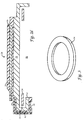
- semiconductor substrates 42 are generally circular, the magnetic shunt 34 is typically annular, with an external diameter corresponding to the diameter of the substrate 42 .
- a suitable annular magnetic shunt 34 is shown in Figure 3.
- the shunt 34 has an internal diameter of at least about 100 mm (4 inches), and an external diameter of at least about 225 mm (8 inches).
- the thickness of the shunt 34 varies according to the distance between the shunt 34 and the substrate 42 , and the magnetic permeability of the magnetic shunt 34 .
- a thinner shunt can be used when the magnetic shunt 34 is positioned close to the substrate 42 .
- a suitable thickness for a nickel containing shunt positioned about 10 mm from the substrate 42 is from about 100 ⁇ m to about 1,000 ⁇ m.
- the shape of the continuous magnetic shunt can differ considerably for non-conventional etching processes.
- other etching processes can require a shunt 34 which is segmented into thicker and thinner segment portions to selectively enhance or reduce the magnetic shunting effect at different portions of the substrate 42 .
- the magnetic shunt 34 can be positioned in different portions of the chuck 20 .
- the shunt 34 is positioned above the base 22 of the chuck 20 , and below the top surface of the insulator 26 , so that the shunt is close to the substrate 42 held on the chuck.
- the proximity of the shunt 34 to the substrate 42 increases the shunting effect of the magnetic shunt.
- a thinner shunt can provide equivalent magnetic shunting.
- thinner magnetic shunts also promote more uniform, and faster, heat transfer between the substrate 42 and the support 44 , thereby allowing faster and more uniform control of the temperature of the substrate 42 .
- FIG. 2a Several different chuck configurations allow the magnetic shunt to be close to the substrate 42 , as shown in Figures 2a-2d .
- the shunt is positioned directly in contact with the base 22 .
- This configuration allows the shunt 34 to be fabricated as an integral part of the base 22 .
- the shunt 34 can be fabricated by coating the upper surface of the base 22 using a ferromagnetic material, such as by electroplating, as described below in further detail.
- the shunt 34 is an integral part of the base 22 , substantially higher heat transfer rates are obtained between the substrate 42 and the support 44 .
- the magnetic shunt is embedded within the insulator 26 .
- the shunt 34 can be shaped as a ring surrounding a disc-shaped electrode 24.
- the shunt 34 and electrode 24 can be an unitary element.
- the shunt 34 can be integrated with the electrode 24 as shown in Fig. 1 , such as for example when the electrode 24 comprises a ferromagnetic material.
- the shunt 34 is embedded in the insulator 26 on the chuck 20 .
- the magnetic shunt 34 is positioned in substrate support 70 on the base 22.
- the substrate support 70 has a top surface adapted for supporting a substrate 42 , and the support 70 includes a cavity 72 therein.
- the substrate support 70 comprises peripheral sidewalls 74 extending upwardly from the base 22 .
- a cover plate 76 is sized to fit over the sidewall 74 and forms the top surface of the substrate support 70.
- the magnetic shunt 34 is sized to fit within the substrate support 70 . This configuration allows the shunt 34 to be adapted to provide optimal shunting for specific substrate processes.
- the magnetic shunt 34 is disposed directly below, and contiguous to, the base 22 .
- the base 22 has a cavity 80 under the base.
- the support member 32 extends into the cavity 80 , and is provided for supporting the high voltage electrical connector 30 .
- the continuous annular magnetic shunt 34 extends into the gap 82 between the support member 32 and the base 22 .
- the cavity 80 is defined by a peripheral wall 84 extending downwardly from the base 22 .
- a preferred process for making an electrostatic chuck 20 according to the present invention is described below.
- the process of making the version of the chuck 20 shown in Figure 2a will be described, and thereafter, the processes of manufacture for making the other versions of the chuck will be described.
- the version of the chuck shown in Figure 2a generally comprises: (a) a base 22 having an upper surface adapted to support a substrate thereon, (b) an insulator 26 with an electrode 24 embedded therein on the base 22 , and (c) a magnetic shunt 3 4 comprising a ferromagnetic material on the base 22 , at least a portion of the shunt 34 being contiguous with the insulator 26 .
- the base 22 of the chuck 20 is typically machined from an aluminum plate, cut into a right-cylindrical shape with a thickness of about 1.5 to 1.8 cm and a diameter of about 100 to 300 mm, to match the diameter of the substrate which typically ranges from about 127 to 203 mm (5 - 8 inches).
- the top and bottom surfaces of the aluminum plate are ground using conventional aluminum grinding techniques, until the surface roughness of the plate is less than about 1 ⁇ m. Surface grinding of the plate is essential for the base to uniformly contact the support 44 , and the substrate placed on the base 22 , to allow for efficient thermal transfer between the substrate 42 and the support 44 . After grinding, the plate is thoroughly cleaned to remove grinding debris.
- a magnetic shunt 24 comprising a ferromagnetic material, is formed above, and in direct contact with the base 22 .
- the magnetic shunt 34 can be formed by a variety of different techniques, including electroplating, chemical vapor deposition, and physical vapor deposition techniques such as sputter coating. Suitable electroplating techniques for electroplating iron or nickel or alloys thereof, are generally described in U.S. Patent nos. 5,160,423 to Yokoi; 4,960,653 to Yokoi; 4,780,342 to LeBlanc; 3,617,343 to Kandler; and 3,655,532 to Marker, all of which are incorporated herein by reference.
- the insulated electrode 24 is separately fabricated and adhered over the shunt 34 .
- the insulated electrode 24 can be fabricated by numerous techniques, such as for example, those disclosed in aforementioned U.S. patent application no. 08/189,562.
- a preferred method uses a multilayer film, comprising an insulative layer and an electrically conductive electrode layer, such as "R/FLEX 1100" film fabricated by Rogers Corporation, Chandler, Arizona, which comprises a layer of copper on a 25 to 125 ⁇ m thick polyamide insulator layer.
- the copper layer of the multi-layer film is etched, routed, or milled to form a patterned electrode shape. Any conventional etching process can be used to etch the copper layer to form an electrode 24 .
- a uniform layer of photoresist material such as "RISTON” fabricated by DuPont de Nemours Chemical Co., Wilmington, Delaware, is applied on the electrode layer.
- photoresist material such as "RISTON” fabricated by DuPont de Nemours Chemical Co., Wilmington, Delaware
- Conventional photolithographic methods such as those described in U.S. Patent No. 4,952,528, to Abe, et al., U.S. Patent No. 5,079,600, to Schnur, et al., U.S. Patent No. 5,221,422, to Das, et al. all of which are incorporated herein by this reference, are then used to form a patterned protective resist layer on the copper layer.
- the electrode layer with the patterned photoresist thereon is then etched, using wet or dry chemical etching methods.
- a suitable wet chemical etching method comprises immersing the electrode layer of the film into an etchant such as ferric chloride, sodium persulfate, or an acid or base, until the electrode layer is etched. Suitable dry etching processes are described in U.S. Patent Nos.
- a second insulative film is adhered over the patterned copper layer so that the copper layer is embedded within the insulative layer.
- Suitable insulative films include, "KAPTON”, a polyamide film manufactured by DuPont de Nemours Co., in Wilmington, Delaware; “APIQUEO” fabricated by Kanegafuchi Chemical Indus., Japan; “UPILEX” manufactured by Ube Indus. Ltd., Japan; “NITOMID” fabricated by Nitto Electric Indus. Co. Ltd., Japan; and "SUPERIOR FILM” fabricated by Mitsubishi Plastics Indus. Ltd., Japan.
- the grooves 36 through the insulator 26 are typically formed by stamping out a suitable groove pattern through the insulated electrode.
- the stamped out insulated electrode 24 is then adhered to the base 22 using conventional pressure or temperature based adhesives, to form the chuck shown in Figure 2a .
- an insulated electrical connector strap 28 is then affixed to a segment of the electrode 24 using electrically conductive adhesive.
- the electrical connector strap 28 is adhered to the base 22 and to the support member 32 on the bottom of the base 22 , using conventional temperature and pressure based adhesives.
- a high voltage electrical connector 30 is then electrically adhered to the electrical strap 28 to form a high voltage connector on the bottom of the base 22 , for connecting the electrode 24 of the chuck 20 to the external voltage supply 46 .
- the version of the chuck shown in Figure 2b can be fabricated by the following procedure.
- An electrically insulative polymer film such as for example, "KAPTON”, “APIQUEO”, “UPILEX”, “NITOMID” films as previously described, is selected, and the electrode 24 and magnetic shunt 34 layers are formed on the insulative film.
- the electrode 24 and shunt 34 layers can be formed by many different techniques, including for example, electroplating, chemical vapor deposition, and physical vapor deposition methods.
- a preferred method of forming the layers comprises a multi-step electroplating process which includes the steps of: (i) sputter depositing a "seed" chromium layer onto the insulative layer, (ii) coating the sputtered chromium layer with a resist layer, (iii) patterning the resist layer into a pattern corresponding to the desired electrode or shunt configuration, and (iv) electroplating metal onto the portions of the chromium seed layer which are not coated by resist to form the electrode or shunt.
- the process is performed twice, once for electroplating the electrode 24 , and the second time for electroplating the shunt 34 .
- the process is performed once.
- a chromium layer is sputtered over the insulative film to obtain a "seed" layer for nucleating growth of the electroplated metal.
- the chromium layer is typically sputtered to a thickness of about 100 - 200 ⁇ m.
- Conventional chromium sputtering techniques are suitable, such as for example, those generally disclosed in U.S. Patent No. 4,131,530; U.S. Patent No. 4,022,947; U.S. Patent No. 4,392,992; and J. A. Thorton, "Sputter Deposition Onto Plastics," Proceedings 18th American Conference of Society of Vacuum Coaters, Key Biscayne, Florida, April 7-9 (1975), pages 8-26.
- a resist layer such as "RISTON” photoresist fabricated by DuPont de Nemours Chemical Co., Wilmington, Delaware, is applied over the chromium "seed” layer.
- Photolithographic methods such as those previously described, are used to pattern the photoresist layer into a pattern corresponding to the desired configuration for the electrode 24 or shunt 34 .
- the patterned resist layer prevents the deposition of electroplated metal on the resist-coated portions, during the electroplating step.
- the resist-coated insulative film is electroplated to form a patterned electrode 24 between the resist-coated portions.
- Conventional copper plating techniques are suitable for forming the electrode 24 , such as for example those disclosed in U.S. Patent No. 5,252,196, to Sonnenberg, et al.; U.S. Patent No. 5,004,525, to Bernards, et al.; U.S. Patent No. 4,898,647, to Luce, et al.; and U.S. Patent No. 4,948,474, to Miljkovic.
- Conventional nickel plating techniques are suitable for forming the shunt 34 , such as for example those disclosed above.
- a suitable wet chemical etching method comprises immersing the chuck 20 into a solution of N-methylpyrolidone heated to 80°C for about ten minutes.
- a plasma etching techniques such as those utilizing an oxygen plasma, as generally disclosed in U.S. Patent No. 3,837,856, to Irving, et al.; U.S. Patent No. 4,786,578, to Neisius, et al.; and U.S. Patent No. 4,938,839, to Fujimura, et al.
- a second electrically insulative film is then applied over the electrode 24 and shunt 34 in the form of a sheet of insulative material (as described above), or by spraying, dipping, painting, spin coating, or silk screening an electrically insulative liquid onto the exposed electrode and shunt.
- a sheet of insulative material is applied, the insulative sheet is sized sufficiently large to cover the entire electrode and shunt.
- the grooves 36 can be formed by etching a groove pattern into upper insulative layer.
- the viscous liquid insulative material flows into the trenches between the electrode 24 and shunt 34 forming the grooves 36 .
- the electrode 24 and shunt 34 can also be formed by the steps of: (i) depositing a continuous metal layer on the insulative layer by chemical or physical vapor deposition techniques; (ii) forming a patterned resist layer on the metal layer, using the conventional techniques disclosed above; and (iii) etching the portions of the metal layer that are exposed between the resist coated portions, by a wet chemical or plasma activated etching process.
- Suitable chemical etching processes are generally described in U.S. Patent No. 3,615,951, to Franco, et al.; U.S. Patent No. 5,100,499, to Douglas; U.S. Patent No. 5,167,748, to Hall, et al.; U.S. Patent No.
- the versions of the invention shown in Figures 2c and 2d are fabricated using substantially the same techniques as described above, with the exception that the magnetic shunt 34 is formed as a separate piece.
- the magnetic shunt is machined from a plate of ferromagnetic material, such as nickel, using conventional machining techniques.
- the base 22 of the chuck shown in Figure 2d is formed by machining an aluminum plate into the desired shape.
- the electrical connector support member 32 can be formed by aluminum welding the support member onto the base 22 , and thereafter, grinding the bottom surface of the base 22 to obtain a smooth contact surface.
- a process according to the present invention is effected on a substrate 42 comprising a semiconductor wafer, such as a silicon or a gallium arsenide wafer.
- the process chamber 40 is evacuated to a pressure ranging from about 0,1333 to about 66,65 Pa (1 to about 500 mTorr), and more typically from about 1,333 to about 13,33 Pa (10 to about 100 mTorr).
- a substrate 42 is transferred to the chamber 40 from a load lock transfer chamber (not shown), and placed on an electrostatic chuck 20 on a support 44 in the chamber 40 .
- Etchant process gas is introduced in the process chamber 40 using one or more sources of pressurized gas.
- Conventional halogen-containing etchant gases such as for example, Cl2, BCl3, CCl4, SiCl4, CF4, NF3, and mixtures thereof, can be used to etch the substrate, as generally described in S. Wolf and R. N. Tauber, Silicon Processing for the VLSI Era , Vol. I, Chap. 16: Dry Etching for VLSI, Lattice Press, Sunset Beach, California (1986), which is incorporated herein by reference.
- the voltage supply 48 is then activated to electrically bias the support 44 with respect to the grounded surface 50 , thereby forming a plasma from the process gas in the chamber 40 .
- An alternating current is applied through the coil 54 around the chamber 40 to generate a magnetic field in the chamber 40 for enhancing the uniformity of the etching plasma in the chamber 40 .
- the plasma activated etchant species impinge upon and etch the substrate 42 .
- the magnetic shunt 34 in the electrostatic chuck 20 depletes those portions of the magnetic field above the magnetic shunt 34 , thereby precluding excessive etching of the substrate 42 at these regions and providing more uniform etching of the substrate 42 .
- the magnetic shunt 34 also allows more uniform heat transfer from the substrate 42 thereby further enhancing etching uniformity.
- a portion of the base can be made from a ferromagnetic material to serve as the magnetic shunt.
- the chuck can be used in other processes such as a chemical vapor deposition, physical vapor deposition, or sputtering processes. Therefore, the spirit and scope of the appended claims should not be limited to the description of the preferred versions contained herein.
Abstract
An electrostatic chuck (20) for holding substrates (42) in a process chamber (40) containing a magnetic flux (43) comprises a base (22) having an upper surface adapted to support a substrate (42) thereon. An insulator (26) with an electrode (24) therein, is on the base (22). A magnetic shunt (34) comprising a ferromagnetic material is positioned (i) either on the base (22), or (ii) in the insulator (26), or (iii) directly below, and contiguous to, the base (22).
Description
- This invention relates to an electrostatic chuck for holding a substrate in a process chamber containing a magnetic flux.
- In semiconductor fabrication processes, electrostatic chucks are used to hold substrates, such as silicon wafers, during processing of the substrate. Electrostatic chucks are generally described in, for example, U.S. Patent No. 4,184,188, to Briglia; U.S. Patent No. 4,399,016, to Tokuda; U.S. Patent No. 4,384,918, to Abe; and U.S. S.N. 08/189562 (copy enclosed), entitled "Electrostatic Chuck" by Shamouilian, et al., filed on January 31, 1994 -- all of which are incorporated herein by reference.
- A typical electrostatic chuck comprises a base adapted to be secured to a support in a process chamber. An electrically insulated electrode is on the base, and underside of the base typically comprises a cavity. An electrical connector electrically connects the insulated electrode on the base to an electrical contact on the bottom of the base. The electrical contact is supported by a support member which extends into the cavity of the base.
- During its use, the chuck is secured to a support in a process chamber, so that the electrical contact on the bottom of the base electrically contacts a voltage supply connector on the support. A substrate is placed on the upper surface of the chuck, and the electrode in the chuck is electrically biased with respect to the substrate by a voltage applied via the electrical contact of the chuck. The applied voltage causes electrostatic charge to accumulate in the insulated electrode of the chuck and in the substrate, and the resultant electrostatic force holds the substrate to the chuck.
- Electrostatic chucks are used in semiconductor fabrication processes, such as deposition processes and etching processes. In a typical etching process, etchant process gas is introduced in the process chamber, and a plasma is formed from the process gas for etching the substrate. During the etching process, a magnetic flux can be generated in the process chamber to enhance the uniformity and rate of etching of the substrate. Typically, the magnetic flux has a component which is parallel to the surface of the substrate. The magnetic field confines electrons and reactive species near the surface of the substrate thereby increasing ionizing collisions. In such etching processes, the peripheral portions of the substrate are typically etched faster than the central portions of the substrate, because etchant gas ingress, and gaseous byproduct removal, are faster at the peripheral substrate regions.
- In such etching processes an annular magnetic shunt, positioned in the cavity on the underside of the base can be used to control the rate of etching of the peripheral portions of the substrate which are adjacent to the annular magnetic shunt. The magnetic shunt typically comprises a ferromagnetic material which attracts the magnetic flux, thereby causing the magnetic flux above the shunt to be redirected toward the shunt, instead of parallel to the substrate surface. The resultant depletion of magnetic flux above the peripheral portions of the substrate reduces the rate of etching of the substrate at these regions. In this manner, magnetic shunts are used to control etch rates across the substrate surface, to obtain more uniform etching of the substrate. More uniform substrate etching provides higher IC chip yields and allows utilization of the entire substrate surface.
- However, there are several problems with conventional magnetic shunt configurations. One problem is that conventional magnetic shunts do not uniformly deplete the magnetic flux above the substrate. It is believed that the non-uniform depletion results from discontinuities and cutaways in the conventional shunts. Conventional shunts are typically positioned in the cavity of the base, and are configured to circumvent projections, such as supports, projections, water cooling tubes, and screw holders in the base. The discontinuities in the magnetic shunt result in non-uniform etch rates across the periphery of the substrate.
- Another problem with conventional magnetic shunts is that the shunts result in non-uniform heat transfer rate between the substrate and the support, because the heat transfer rates differ between the continuous and discontinuous portions of the shunt. Non-uniform heat transfer rates result in non-uniform temperatures across the surface of the substrate, resulting in non-uniform etch rates.
- Thus, it is desirable to have electrostatic chuck and magnetic shunt configuration that allows uniform magnetic shunting across the surface of the wafer, and allows uniform heat transfer between the substrate and the support. It is also desirable for the magnetic shunt to be disposed proximate to the substrate to enhance magnetic shunting through the substrate.
- The present invention intends to overcome these problems. The object is solved by the electrostatic chuck according to independent claims 1, 4, 5, 6, 19, the process chamber of independent claim 8 and the method of forming an electrostatic chuck according to
independent claim 28. - Further advantages, features, aspects and details of the invention are evident from the dependent claims, the description and the accompanying drawings. The claims are intended to be understood as a first non-limiting approach to defining the invention in general terms.
- An electrostatic chuck of the present invention satisfies these needs. The electrostatic chuck comprises a base having an upper surface adapted to support a substrate thereon. An insulator with an electrode therein, is on the base. A magnetic shunt comprising a ferromagnetic material is disposed above the base, or disposed directly below and contiguous to the base. When the chuck is used to electrostatically hold a substrate in the process chamber containing a magnetic flux, the magnetic shunt in the chuck causes the magnetic flux in the chamber to be depleted above those portions of the substrate which are proximate to the magnetic shunt. This results in more uniform processing of the substrate held by the chuck.
- Several configurations of the magnetic shunt are possible. In one configuration, the magnetic shunt is positioned between the base and the insulator, and in direct contact with the base. In another configuration, the magnetic shunt is in the insulator. In a third version of the invention, the electrode in the insulator comprises a ferromagnetic material which operates as a magnetic shunt.
- In another configuration, a substrate support adapted for supporting a substrate is on the base of the chuck. The substrate support includes a cavity therein, and an insulated electrode is on the substrate support. A ferromagnetic magnetic shunt is within the cavity of the substrate support.
- In another version of the invention, a continuous magnetic shunt is disposed directly below, and contiguous to the base.
- The magnetic shunts are preferably continuously annular. Preferably, the magnetic shunts are made of a ferromagnetic material such as iron, nickel, cobalt, and alloys thereof.
- The present invention will become better understood with reference to the following description and accompanying drawings, where:
- Figure 1 is a cross-sectional, side elevational schematic view of a processing chamber containing an electrostatic chuck of the present invention;
- Figure 2a is a cross-sectional, side elevational view of a chuck of the present invention, showing a magnetic shunt above the base of the chuck;
- Figure 2b is a cross-sectional, side elevational view of another version of the chuck of the present invention, showing a magnetic shunt in the insulator of the chuck;
- Figure 2c is a cross-sectional, side elevational view of another version of the chuck of the present invention, showing a magnetic shunt positioned in a substrate support on the base of the chuck;
- Figure 2d is a cross-sectional, side elevational view of another version of the chuck of the present invention, showing a continuous magnetic shunt positioned in the cavity of the base of the chuck; and
- Figure 3 is a perspective view of a continuous magnetic shunt of the present invention.
- An
electrostatic chuck 20 of the present invention generally comprises abase 22 with an electrically insulatedelectrode 24 on the base. The electrode is electrically isolated by aninsulator 26. Anelectrical connector strap 28 electrically connects theelectrode 24 on the chuck to a high voltageelectrical connector 30 on the base of thechuck 20. The high voltageelectrical connector 30 is supported by asupport member 32. Amagnetic shunt 34 is placed above, or directly below, and contiguous to, thebase 22 of the chuck. Thechuck 20 can also havegrooves 36 therein, thegrooves 36 being provided for holding a coolant gas therein, for cooling a substrate held by the chuck. - With reference to Figure 1, operation of the
chuck 20 of the present invention will now be described. Figure 1 shows atypical process chamber 40 containing a magnetic flux, which can be used to process asubstrate 42, such as a silicon wafer. Typically, the magnetic flux has a component in a plane parallel to the direction of thearrows 43. The particular embodiment of theprocess chamber 40 shown herein is suitable for plasma processing ofsubstrates 42, and is provided only to illustrate operation of thechuck 20, and should not be used to limit the scope of the invention. - The
process chamber 40 generally comprises asupport 44 with theelectrostatic chuck 20 on thesupport 44. An externalfirst voltage supply 46 is connected to theelectrode 24 in the chuck and provides a voltage for operating thechuck 20. Thefirst voltage supply 46 comprises a high voltage DC source of about 1000 to 3000 volts, connected to a high voltage readout, through a 10 MΩ resistor. The 1 MΩ resistor in the circuit limits the current flowing though the circuit, and a 500 pF capacitor is provided as an alternating current filter. - An external
second voltage supply 48 is connected to thesupport 44 in the chamber. Thesupport 44 in theprocess chamber 40 is typically made from aluminum and functions as a process electrode for forming a plasma in the chamber. Thesecond voltage supply 48 is provided for electrically biasing thesupport 44 with respect to an electrically groundedsurface 50 in thechamber 42 for forming the plasma in thechamber 40. Thevoltage supply 48 is conventional and generally comprises an RF impedance that matches impedance of theprocess chamber 40 to the impedance of the line voltage, in series with an isolation capacitor, as shown in Figure 1. - A
coolant source 52 can be used to remove heat from thesubstrate 42, to maintain thesubstrate 42 at a constant temperature. - The
process chamber 40 also hascylindrical coils 54 wrapped around thechamber 42. Thecoils 54 are connected to an alternatingcurrent source 56. When an alternating current is applied through thecoils 54, thecoils 54 establish a magnetic field having a component withmagnetic flux lines 43 substantially parallel to the surface of thesubstrate 42 in thechamber 40. During processing of thesubstrate 42, the alternating current through thecoils 54 is varied so that the magnetic flux lines rotate in a plane parallel to the surface of the substrate to produce a more uniform time-averaged magnetic field in theprocess chamber 40. The time-averaged magnetic field provides a more uniform plasma density thereby allowing more uniform etch rates across the surface of thesubstrate 42. - During its use, the
chuck 20 is placed on thesupport 44. Asubstrate 42 is placed on thechuck 20, and theelectrode 24 is electrically biased with respect to the substrate by a voltage applied by thefirst voltage supply 44, so that electrostatic charge accumulates in thesubstrate 42 and in theelectrode 24, causing the substrate to be electrostatically held to thechuck 20. Themagnetic shunt 34 attracts the magnetic flux above the shunt, as diagrammatically shown by thearrows 58, causing depletion of the magnetic flux above those portions of thesubstrate 42 that are proximate to theshunt 34. Typically, themagnetic shunt 34 comprises ferromagnetic material distributed in a configuration which concentrates ferromagnetic material toward the periphery of theinsulator 26. - Particular aspects of the
chuck 20 will now be discussed in detail. - The
base 22 of the chuck is provided for supporting theinsulated electrode 24. Generally, thebase 22 has a shape and size corresponding to the shape and size of thesubstrate 42 to maximize the heat transfer surface between the base and thesubstrate 42, and to provide a wide surface for holding thesubstrate 42. For example, if thesubstrate 42 is disk shaped, a cylindrically shaped base having an upper surface sized for supporting a substrate. Alternatively, thebase 22 can have a shape different from the shape of thesubstrate 42 or a size different from the size of thesubstrate 42. Typically, the base is made from a non-ferromagnetic material, such as aluminum. Typically, the base is a right cylinder having a diameter of about 100 mm to 225 mm (4 to 9 inches), and a thickness of about 1.5 to 2 cm. - The size and shape of the
insulated electrode 24 on the base also varies according to the size and shape of thesubstrate 42. For example, as shown in the drawings, if thesubstrate 42 is disc-shaped, theinsulated electrode 24 is also disc-shaped to maximize the area of the electrode in contact with thesubstrate 42. The top surface of theinsulator 26 of theelectrode 24, is adapted to support asubstrate 42 thereon. Theelectrode 24 is made from an electrically conductive material, such as metal, for example, copper, nickel, chromium, aluminum, iron, and alloys thereof. Typically, the thickness of theelectrode 24 is from about 1 µm to 100 µm, and more typically from about 1 µm to 30 µm. - The
electrode 24 be continuous as shown in Figure 1, or can be patterned as shown in Figure 2. Preferably, theelectrode 24, is patterned into one of several alternative configurations. In one patterned configuration, theelectrode 24 forms interconnected features, the features sized so that thegrooves 36 can be formed between the electrode features, thegrooves 36 provided for holding a coolant therein for cooling thesubstrate 42. - In another configuration, the patterned
electrode 24 comprises at least one pair of electrodes, so that theelectrode 24 can function as a bipolar electrode. Suitable bipolar electrode configurations are disclosed in U.S. Patent Nos. 4,184,188 to Briglia; 4,384,918 to Abe; and Tsukada et al., -- all of which are incorporated herein by reference. When abipolar electrode 24 configuration is used, voltages are applied to each of the pair of electrodes, to maintain the pair of electrodes at opposite polarities. The bipolar electrode configurations allows accumulation of electrostatic charge in thesubstrate 42, without electrically biasing the substrate. Bipolar electrode configurations can be advantageous when thechuck 20 is used for non-plasma processes, where there are no charged plasmas species that serve as change carriers for electrically basing thesubstrate 42. - The
electrode 24 is electrically isolated from thechuck 20 by theinsulator 26. Theinsulator 26 typically comprises a synthetic polymer such as polyimide, polyketone, polyetherketone, polysulfone, polycarbonate, polystyrene, nylon, polyvinylchloride, polypropylene, polyetherketones, polyethersulfone, polyethylene terephthalate, fluoroethylene propylene copolymers, cellulose, triacetates, silicone, and rubber. - The overall thickness of the
insulator 26 varies according to the electrical resistivity and dielectric constant of the insulative material used to form theinsulator 26. Typically, the insulative material has a resistivity ranging from about 10¹³ Ω cm to 10²⁰ Ω cm, and a dielectric constant of at least about 2, and more preferably at least about 3. When the insulative material has a dielectric constant of about 3.5, theentire insulator 26 is typically about 10 µm to about 500 µm thick, and more typically from about 100 µm to about 300 µm thick. - When a polyimide is used as the
insulator 26, the insulator has a dielectric breakdown strength of at least about 3.9 volts/µm (100 volts/mil), and more typically at least about 39 volts/µm (1000 volts/mil). - Preferably, the top of
insulator 26 is resistant to temperatures in excess of 50°C, and more preferably resistant to temperatures in excess of 100°C, so that thechuck 20 can be used in processes where thesubstrate 42 is heated. Also, preferably, the insulative material has a high thermal conductivity so that heat generated in thesubstrate 42 during processing can dissipate through thechuck 20. The thermal conductivity of theinsulator 26 should be at least about 0.10 Watts/m/oK, to allow sufficient heat transfer to preclude overheating of thesubstrate 42. - The insulative material can also include high a thermal conductivity filler material, such as diamond, alumina, zirconium boride, boron nitride, and aluminum nitride for increasing the thermal conductivity and resistance to plasma corrosion. Preferably the filler material is a powder with an average particle size of less than about 10 µm. Typically, the filler is dispersed in the insulative material in a volumetric ratio from about 10% to 80%, and more typically from about 20% to 50%.
- Preferably, the top of the
insulator 26 has spaced apartgrooves 36 therein, thegrooves 36 sized and distributed to hold coolant from acoolant source 52 for cooling thesubstrate 42. Thegrooves 36 can form as a pattern of intersecting trenches, the trenches lying between the features of theelectrodes 24. Alternative groove patterns are described in for example, "Electrostatic Chuck" by Shamouilian, et al., as referenced above. - Additionally, a protective coating (not shown) can be applied on top of the
insulator 26 to protect theinsulator 26 from chemical degradation when thechuck 20 is used in corrosive processing environments. Preferred protective coatings and processes for their fabrication are described in more detail in for example U.S. Patent Application S/N 08/052,018, filed on February 22, 1993, entitled "PROTECTIVE COATING FOR DIELECTRIC MATERIAL ON WAFER SUPPORT USED IN INTEGRATED CIRCUIT PROCESSING APPARATUS AND METHOD OF FORMING THE SAME," by Wu, et al., which is incorporated herein by this reference. - The
chuck 20 also comprises an electrical connector for connecting theelectrode 24 to thefirst voltage supply 46. The electrical connector comprises an electricallyconductive strap 28 which connects the insulated electrode to a high voltageelectrical connector 30 on the bottom of thebase 22. The high voltageelectrical connector 30 rests on asupport member 32 which extends into a cavity in thebase 22, as shown in Figure 2d. - Preferably, the
magnetic shunt 34 of thechuck 20 is continuous, with no breaks or discontinuities therebetween. This is a significant improvement over the prior art. Prior art shunts which are discontinuous, result in non-uniform etching of thesubstrate 42, at those portions of thesubstrate 42 adjacent to the discontinuity in the shunt. Inherent limitations in prior art chuck configurations necessitated that prior art magnetic shunts have breaks and discontinuities therein. The magnetic shunt and chuck assembly of the present invention avoids the prior art limitations by allowing use of a continuous magnetic shunt. - It is believed that a continuous
magnetic shunt 34 is advantageous because it would uniformly deplete the magnetic flux above the periphery of thesubstrate 42, thereby resulting in more uniform etch rates across the substrate surface. Another advantage of thecontinuous shunt 34 is that the shunt can allow uniform heat transfer from thesubstrate 42 to thesupport 44, resulting in uniform temperatures across the surface of thesubstrate 42. - The
magnetic shunt 34 is typically made from a ferromagnetic material that has an high relative magnetic permeability, such as nickel, iron, cobalt, and alloys thereof. Magnetic permeability (µ) is defined as the magnetic flux density B (magnetic induction) produced in a material by a magnetic field, divided by the intensity of the magnetic field H. Relative magnetic permeability µr is the ratio of the permeability of the material to the permeability of air:
- Ferromagnetic materials have a relative magnetic permeability of at least about 100, more typically at least about 500, and most typically at least about 1000. The relative magnetic permeability value depends upon the value of H and the previous magnetic history of the material. Typically, ferromagnetic materials, such as iron, nickel and cobalt, have a value of µ of at least about 1 thousand. Conventional techniques can be used to measure the magnetic permeability of materials, such as for example, Rowland Ring methods and Permeameters.
- The high magnetic permeability of the
magnetic shunt 34 causes the shunt to exhibit low inductance to themagnetic flux lines 43 in theprocess chamber 40. This causes themagnetic shunt 34 to attract themagnetic flux lines 43 above the shunt, thereby depleting the magnetic flux above the portions of thesubstrate 42 proximate to the magnetic shunt, as shown in Figure 1. - The
magnetic shunt 34 is configured to correspond to the shape and size of the those portions of the substrate that exhibit excessive etching rates. Excessive etching rates are determined by etching substrates using conventional etching processes, and mapping out the regions of excessive etching by examining the etched substrates in a scanning electron microscope. Thus, the shape and size of themagnetic shunt 34 depends on the etching characteristics of the particular process chamber, the process gases and process conditions used to etch the substrate, and shape and size of thesubstrate 42. - In the most conventional etching processes, the periphery of the
substrate 42 is etched faster than the central portions of thesubstrate 42. Thus, the magnetic shunt is typically configured to preferentially concentrate ferromagnetic material toward the periphery of thesubstrate 42. Becausesemiconductor substrates 42 are generally circular, themagnetic shunt 34 is typically annular, with an external diameter corresponding to the diameter of thesubstrate 42. - A suitable annular
magnetic shunt 34 is shown in Figure 3. Theshunt 34 has an internal diameter of at least about 100 mm (4 inches), and an external diameter of at least about 225 mm (8 inches). The thickness of theshunt 34 varies according to the distance between theshunt 34 and thesubstrate 42, and the magnetic permeability of themagnetic shunt 34. A thinner shunt can be used when themagnetic shunt 34 is positioned close to thesubstrate 42. A suitable thickness for a nickel containing shunt positioned about 10 mm from thesubstrate 42, is from about 100 µm to about 1,000 µm. - The shape of the continuous magnetic shunt can differ considerably for non-conventional etching processes. For example, other etching processes can require a
shunt 34 which is segmented into thicker and thinner segment portions to selectively enhance or reduce the magnetic shunting effect at different portions of thesubstrate 42. - The
magnetic shunt 34 can be positioned in different portions of thechuck 20. Preferably, theshunt 34 is positioned above thebase 22 of thechuck 20, and below the top surface of theinsulator 26, so that the shunt is close to thesubstrate 42 held on the chuck. The proximity of theshunt 34 to thesubstrate 42 increases the shunting effect of the magnetic shunt. Also, because the base does not lie between the shunt and the substrate, a thinner shunt can provide equivalent magnetic shunting. Furthermore, thinner magnetic shunts also promote more uniform, and faster, heat transfer between thesubstrate 42 and thesupport 44, thereby allowing faster and more uniform control of the temperature of thesubstrate 42. - Several different chuck configurations allow the magnetic shunt to be close to the
substrate 42, as shown in Figures 2a-2d. In the configuration shown in Figure 2a, the shunt is positioned directly in contact with thebase 22. This configuration allows theshunt 34 to be fabricated as an integral part of thebase 22. For example, theshunt 34 can be fabricated by coating the upper surface of the base 22 using a ferromagnetic material, such as by electroplating, as described below in further detail. Also, because theshunt 34 is an integral part of thebase 22, substantially higher heat transfer rates are obtained between thesubstrate 42 and thesupport 44. - In the configuration shown in Figure 2b, the magnetic shunt is embedded within the
insulator 26. In this configuration, theshunt 34 can be shaped as a ring surrounding a disc-shapedelectrode 24. Alternatively, theshunt 34 andelectrode 24 can be an unitary element. Also, theshunt 34 can be integrated with theelectrode 24 as shown in Fig. 1, such as for example when theelectrode 24 comprises a ferromagnetic material. In these configurations, theshunt 34 is embedded in theinsulator 26 on thechuck 20. These latter configurations are advantageous because they allow fabrication of the shunt and electrode as a single element, thereby lowering fabrication and assembly costs for thechuck 20. - In the configuration shown in Figure 2c, the
magnetic shunt 34 is positioned insubstrate support 70 on thebase 22. Thesubstrate support 70 has a top surface adapted for supporting asubstrate 42, and thesupport 70 includes acavity 72 therein. Typically, thesubstrate support 70 comprisesperipheral sidewalls 74 extending upwardly from thebase 22. Acover plate 76 is sized to fit over thesidewall 74 and forms the top surface of thesubstrate support 70. In this configuration, themagnetic shunt 34 is sized to fit within thesubstrate support 70. This configuration allows theshunt 34 to be adapted to provide optimal shunting for specific substrate processes. - In the configuration shown in Figure 2d, the
magnetic shunt 34 is disposed directly below, and contiguous to, thebase 22. Typically thebase 22 has acavity 80 under the base. Thesupport member 32 extends into thecavity 80, and is provided for supporting the high voltageelectrical connector 30. In the chuck of the present invention, the continuous annularmagnetic shunt 34 extends into thegap 82 between thesupport member 32 and thebase 22. Thecavity 80 is defined by aperipheral wall 84 extending downwardly from thebase 22. - A preferred process for making an
electrostatic chuck 20 according to the present invention, is described below. The process of making the version of thechuck 20 shown in Figure 2a, will be described, and thereafter, the processes of manufacture for making the other versions of the chuck will be described. - The version of the chuck shown in Figure 2a, generally comprises: (a) a
base 22 having an upper surface adapted to support a substrate thereon, (b) aninsulator 26 with anelectrode 24 embedded therein on thebase 22, and (c) amagnetic shunt 34 comprising a ferromagnetic material on thebase 22, at least a portion of theshunt 34 being contiguous with theinsulator 26. - The
base 22 of thechuck 20 is typically machined from an aluminum plate, cut into a right-cylindrical shape with a thickness of about 1.5 to 1.8 cm and a diameter of about 100 to 300 mm, to match the diameter of the substrate which typically ranges from about 127 to 203 mm (5 - 8 inches). The top and bottom surfaces of the aluminum plate are ground using conventional aluminum grinding techniques, until the surface roughness of the plate is less than about 1 µm. Surface grinding of the plate is essential for the base to uniformly contact thesupport 44, and the substrate placed on thebase 22, to allow for efficient thermal transfer between thesubstrate 42 and thesupport 44. After grinding, the plate is thoroughly cleaned to remove grinding debris. - After forming the
base 22, amagnetic shunt 24 comprising a ferromagnetic material, is formed above, and in direct contact with thebase 22. Themagnetic shunt 34 can be formed by a variety of different techniques, including electroplating, chemical vapor deposition, and physical vapor deposition techniques such as sputter coating. Suitable electroplating techniques for electroplating iron or nickel or alloys thereof, are generally described in U.S. Patent nos. 5,160,423 to Yokoi; 4,960,653 to Yokoi; 4,780,342 to LeBlanc; 3,617,343 to Kandler; and 3,655,532 to Marker, all of which are incorporated herein by reference. - The
insulated electrode 24 is separately fabricated and adhered over theshunt 34. Theinsulated electrode 24 can be fabricated by numerous techniques, such as for example, those disclosed in aforementioned U.S. patent application no. 08/189,562. A preferred method uses a multilayer film, comprising an insulative layer and an electrically conductive electrode layer, such as "R/FLEX 1100" film fabricated by Rogers Corporation, Chandler, Arizona, which comprises a layer of copper on a 25 to 125 µm thick polyamide insulator layer. The copper layer of the multi-layer film is etched, routed, or milled to form a patterned electrode shape. Any conventional etching process can be used to etch the copper layer to form anelectrode 24. In the typical etching process, a uniform layer of photoresist material, such as "RISTON" fabricated by DuPont de Nemours Chemical Co., Wilmington, Delaware, is applied on the electrode layer. Conventional photolithographic methods, such as those described in U.S. Patent No. 4,952,528, to Abe, et al., U.S. Patent No. 5,079,600, to Schnur, et al., U.S. Patent No. 5,221,422, to Das, et al. all of which are incorporated herein by this reference, are then used to form a patterned protective resist layer on the copper layer. - The electrode layer with the patterned photoresist thereon is then etched, using wet or dry chemical etching methods. A suitable wet chemical etching method comprises immersing the electrode layer of the film into an etchant such as ferric chloride, sodium persulfate, or an acid or base, until the electrode layer is etched. Suitable dry etching processes are described in U.S. Patent Nos. 3,615,951 to Franco, et al; 5,100,499 to Douglas; 5,167,748, to Hall et al; 5,185,058 to Cathey; 5,200,032, to Shinohara; 5,215,619 to Cheng, et al; and 5,221,430 to Kadomura, et al., all of which are incorporated herein by this reference.
- After etching the electrode layer, a second insulative film is adhered over the patterned copper layer so that the copper layer is embedded within the insulative layer. Suitable insulative films include, "KAPTON", a polyamide film manufactured by DuPont de Nemours Co., in Wilmington, Delaware; "APIQUEO" fabricated by Kanegafuchi Chemical Indus., Japan; "UPILEX" manufactured by Ube Indus. Ltd., Japan; "NITOMID" fabricated by Nitto Electric Indus. Co. Ltd., Japan; and "SUPERIOR FILM" fabricated by Mitsubishi Plastics Indus. Ltd., Japan.
- The
grooves 36 through theinsulator 26 are typically formed by stamping out a suitable groove pattern through the insulated electrode. The stamped outinsulated electrode 24 is then adhered to the base 22 using conventional pressure or temperature based adhesives, to form the chuck shown in Figure 2a. - With reference to Figure 2d, an insulated
electrical connector strap 28 is then affixed to a segment of theelectrode 24 using electrically conductive adhesive. Theelectrical connector strap 28 is adhered to thebase 22 and to thesupport member 32 on the bottom of thebase 22, using conventional temperature and pressure based adhesives. A high voltageelectrical connector 30 is then electrically adhered to theelectrical strap 28 to form a high voltage connector on the bottom of thebase 22, for connecting theelectrode 24 of thechuck 20 to theexternal voltage supply 46. - The version of the chuck shown in Figure 2b, can be fabricated by the following procedure. An electrically insulative polymer film, such as for example, "KAPTON", "APIQUEO", "UPILEX", "NITOMID" films as previously described, is selected, and the
electrode 24 andmagnetic shunt 34 layers are formed on the insulative film. - The
electrode 24 and shunt 34 layers can be formed by many different techniques, including for example, electroplating, chemical vapor deposition, and physical vapor deposition methods. A preferred method of forming the layers comprises a multi-step electroplating process which includes the steps of: (i) sputter depositing a "seed" chromium layer onto the insulative layer, (ii) coating the sputtered chromium layer with a resist layer, (iii) patterning the resist layer into a pattern corresponding to the desired electrode or shunt configuration, and (iv) electroplating metal onto the portions of the chromium seed layer which are not coated by resist to form the electrode or shunt. - When the
electrode 24 andshunt 34 are made of different metals, the process is performed twice, once for electroplating theelectrode 24, and the second time for electroplating theshunt 34. When the electrode and shunt comprise the same metal, the process is performed once. - In the first step of the multi-step electroplating process, a chromium layer is sputtered over the insulative film to obtain a "seed" layer for nucleating growth of the electroplated metal. The chromium layer is typically sputtered to a thickness of about 100 - 200 µm. Conventional chromium sputtering techniques are suitable, such as for example, those generally disclosed in U.S. Patent No. 4,131,530; U.S. Patent No. 4,022,947; U.S. Patent No. 4,392,992; and J. A. Thorton, "Sputter Deposition Onto Plastics," Proceedings 18th American Conference of Society of Vacuum Coaters, Key Biscayne, Florida, April 7-9 (1975), pages 8-26.
- In the next step, a resist layer, such as "RISTON" photoresist fabricated by DuPont de Nemours Chemical Co., Wilmington, Delaware, is applied over the chromium "seed" layer. Photolithographic methods, such as those previously described, are used to pattern the photoresist layer into a pattern corresponding to the desired configuration for the
electrode 24 orshunt 34. The patterned resist layer prevents the deposition of electroplated metal on the resist-coated portions, during the electroplating step. - In the electroplating step, the resist-coated insulative film is electroplated to form a patterned
electrode 24 between the resist-coated portions. Conventional copper plating techniques are suitable for forming theelectrode 24, such as for example those disclosed in U.S. Patent No. 5,252,196, to Sonnenberg, et al.; U.S. Patent No. 5,004,525, to Bernards, et al.; U.S. Patent No. 4,898,647, to Luce, et al.; and U.S. Patent No. 4,948,474, to Miljkovic. Conventional nickel plating techniques are suitable for forming theshunt 34, such as for example those disclosed above. - After forming the
electrode 24 and shunt 34 on thechuck 20, remnant resist and chromium are etched from thechuck 20. Remnant resist is removed by wet chemical etching or plasma etching methods. A suitable wet chemical etching method comprises immersing thechuck 20 into a solution of N-methylpyrolidone heated to 80°C for about ten minutes. Alternatively, a plasma etching techniques, such as those utilizing an oxygen plasma, as generally disclosed in U.S. Patent No. 3,837,856, to Irving, et al.; U.S. Patent No. 4,786,578, to Neisius, et al.; and U.S. Patent No. 4,938,839, to Fujimura, et al. -- all of which are incorporated herein by reference -- can also be used to etch the remnant resist. After removal of the resist remnant, residual chromium is removed by a wet chemical etching step, such as immersing thechuck 20 in a solution of sodium persulfate, followed by immersion in a solution of potassium permanganate. - A second electrically insulative film is then applied over the
electrode 24 and shunt 34 in the form of a sheet of insulative material (as described above), or by spraying, dipping, painting, spin coating, or silk screening an electrically insulative liquid onto the exposed electrode and shunt. When a sheet of insulative material is applied, the insulative sheet is sized sufficiently large to cover the entire electrode and shunt. - When a sheet of insulative material is adhered on the
electrode 24 andshunt 34, thegrooves 36 can be formed by etching a groove pattern into upper insulative layer. Alternatively, when liquid insulative material is applied over the electrode and shunt, the viscous liquid insulative material flows into the trenches between theelectrode 24 and shunt 34 forming thegrooves 36. - Instead of electroplating, the
electrode 24 and shunt 34 can also be formed by the steps of: (i) depositing a continuous metal layer on the insulative layer by chemical or physical vapor deposition techniques; (ii) forming a patterned resist layer on the metal layer, using the conventional techniques disclosed above; and (iii) etching the portions of the metal layer that are exposed between the resist coated portions, by a wet chemical or plasma activated etching process. Suitable chemical etching processes are generally described in U.S. Patent No. 3,615,951, to Franco, et al.; U.S. Patent No. 5,100,499, to Douglas; U.S. Patent No. 5,167,748, to Hall, et al.; U.S. Patent No. 5,185,058, to Cathey; U.S. Patent No. 5,200,032, to Shinohara; U.S. Patent No. 5,215,619, to Cheng, et al.; and U.S. Patent No. 5,221,430, to Kadomura, et al. -- all of which are incorporated herein by reference. - The versions of the invention shown in Figures 2c and 2d are fabricated using substantially the same techniques as described above, with the exception that the
magnetic shunt 34 is formed as a separate piece. Typically, the magnetic shunt is machined from a plate of ferromagnetic material, such as nickel, using conventional machining techniques. - The
base 22 of the chuck shown in Figure 2d is formed by machining an aluminum plate into the desired shape. The electricalconnector support member 32 can be formed by aluminum welding the support member onto thebase 22, and thereafter, grinding the bottom surface of the base 22 to obtain a smooth contact surface. - Referring now to Figure 1, a process according to the present invention is effected on a
substrate 42 comprising a semiconductor wafer, such as a silicon or a gallium arsenide wafer. To effect the process, theprocess chamber 40 is evacuated to a pressure ranging from about 0,1333 to about 66,65 Pa (1 to about 500 mTorr), and more typically from about 1,333 to about 13,33 Pa (10 to about 100 mTorr). Asubstrate 42 is transferred to thechamber 40 from a load lock transfer chamber (not shown), and placed on anelectrostatic chuck 20 on asupport 44 in thechamber 40. - Etchant process gas is introduced in the
process chamber 40 using one or more sources of pressurized gas. Conventional halogen-containing etchant gases, such as for example, Cl₂, BCl₃, CCl₄, SiCl₄, CF₄, NF₃, and mixtures thereof, can be used to etch the substrate, as generally described in S. Wolf and R. N. Tauber, Silicon Processing for the VLSI Era, Vol. I, Chap. 16: Dry Etching for VLSI, Lattice Press, Sunset Beach, California (1986), which is incorporated herein by reference. - The
voltage supply 48 is then activated to electrically bias thesupport 44 with respect to the groundedsurface 50, thereby forming a plasma from the process gas in thechamber 40. An alternating current is applied through thecoil 54 around thechamber 40 to generate a magnetic field in thechamber 40 for enhancing the uniformity of the etching plasma in thechamber 40. The plasma activated etchant species impinge upon and etch thesubstrate 42. - The
magnetic shunt 34 in theelectrostatic chuck 20 depletes those portions of the magnetic field above themagnetic shunt 34, thereby precluding excessive etching of thesubstrate 42 at these regions and providing more uniform etching of thesubstrate 42. Themagnetic shunt 34 also allows more uniform heat transfer from thesubstrate 42 thereby further enhancing etching uniformity. - Although the present invention has been described in considerable detail with reference to certain preferred versions, many other versions should be apparent to those skilled in the art. For example, a portion of the base, can be made from a ferromagnetic material to serve as the magnetic shunt. Also, the chuck can be used in other processes such as a chemical vapor deposition, physical vapor deposition, or sputtering processes. Therefore, the spirit and scope of the appended claims should not be limited to the description of the preferred versions contained herein.
Claims (33)
- An electrostatic chuck (20) for use in a process chamber (40) containing a magnetic flux (43), the chuck comprising:(a) a base (22) having an upper surface adapted to support a substrate (42) thereon;(b) an insulator (26) on the base (22), the insulator having an electrode (24) therein, and(c) a ferromagnetic magnetic shunt (34) above the base (22), whereby, when the chuck (20) is used to electrostatically hold a substrate (42) in the process chamber (40), the magnetic shunt (34) causes the magnetic flux (43) in the chamber to be reduced above portions of the substrate (42) which are proximate to the magnetic shunt (34).
- The electrostatic chuck of claim 1, wherein the ferromagnetic shunt (34) is between the base (22) and the insulator (26), and in direct contact with the base (22).
- The electrostatic chuck of claim 1, wherein the ferromagnetic shunt (34) is within the insulator (26).
- An electrostatic chuck (20) for use in a process chamber (40) containing a magnetic flux especially according to one of the preceding claims, the chuck comprising:(a) a base (22) having an upper surface adapted to support a substrate (42) thereon;(b) an insulator (26) on the base (22); and(c) an electrode (24) in the insulator (26), at least a portion of the electrode (24) comprising a ferromagnetic material for operating as a magnetic shunt (34),
whereby, when the chuck (20) is used to electrostatically hold a substrate (42) in the process chamber (40), the ferromagnetic material in the electrode (24) causes the magnetic flux in the chamber (40) to be reduced above portions of the substrate (42) which are proximate to the electrode (24). - An electrostatic chuck (20) for use in a chamber (40) containing a magnetic flux especially according to one of the preceding claims, the chuck comprising:(a) a base (22);(b) a substrate support (44) on the base (22), the substrate support (44) adapted for supporting a substrate (42) and the substrate support (44) including a cavity (72) therein;(c) an insulated electrode (24) on the substrate support (44); and(d) a magnetic shunt (34) comprising a ferromagnetic material in the cavity (72) of the substrate support (44),
whereby, when the chuck (20) is used to electrostatically hold a substrate (42) in a chamber (40) containing a magnetic flux, the magnetic shunt (34) causes the magnetic flux in the chamber (40) to be reduced above portions of the substrate (42) proximate to the shunt (34). - An electrostatic chuck (20) for use in a chamber (40) containing a magnetic flux especially according to one of the preceding claims, the chuck comprising:(a) a base (22) having an upper surface adapted to support a substrate (42);(b) an insulator (26) having an electrode (24) embedded therein on the base (22); and(c) a continuous annular magnetic shunt (34) comprising a ferromagnetic material, the shunt disposed directly below, and contiguous to, the base (22),
whereby, when the chuck (20) is used to electrostatically hold a substrate (42) in the process chamber (40), the magnetic shunt (34) causes the magnetic flux in the chamber (40) to be reduced above portions of the substrate which are proximate to the shunt (34). - The electrostatic chuck of claim 6, further comprising:(a) a peripheral wall (84) extending downwardly from the base (22), and(b) an electrical connector support (32) extending from the peripheral wall (84), the connector support (32) and base (22) defining a gap (82) therebetween,
wherein a portion of the continuous annular shunt (34) extends into the gap (82) between the connector support (32) and the base (22). - A process chamber (40) for processing substrates (42) in a magnetic flux, the process chamber (40) comprising:(a) a magnetic flux generator for generating a magnetic flux in the process chamber (40); and(b) the electrostatic chuck (20) of one of the preceding claims.
- The electrostatic chuck of one of the preceding claims, wherein the base (22) is a substantially circular plate having a diameter ranging from 15.24 cm to 25.4 cm (6 to 10 inches).
- The electrostatic chuck of one of the preceding claims, wherein the magnetic shunt (34) is circumferentially disposed around the electrode.
- The electrostatic chuck of one of the preceding claims, wherein the annular magnetic shunt (34) has an inside diameter of at least about 100mm.
- The electrostatic chuck of one of the preceding claims, wherein the annular magnetic shunt (34) has an outside diameter of less than about 225 mm.
- The electrostatic chuck of one of the preceding claims, wherein the magnetic shunt (34) has a thickness ranging from about 100 to 1000 µm.
- The electrostatic chuck of one of the preceding claims, wherein the magnetic shunt (34) is continuous.
- The elecrostatic chuck of one of the preceding claims, wherein the magnetic shunt (34) comprises segments.
- The electrostatic chuck of claim 15, wherein the segments in the magnetic shunt (34) have differing thicknesses.
- The electrostatic chuck of one of the preceding claims, wherein the magnetic shunt (34) has a relative magnetic permeability of at least about 1000.
- The electrostatic chuck of one of the preceding claims, wherein the magnetic shunt (34) comprises a material selected from the group consisting of iron, nickel, cobalt, and alloys thereof.
- An electrostatic chuck (20) for use in a process chamber (40) within which a magnetic flux especially according to one of the preceding claims may be established, the chuck comprising:(a) a base (22) of non-ferromagnetic material having an upper support surface;(b) an insulator (26) on the upper surface of the base (22), the insulator (26) having an electrode (24) therein and a top surface adapted to support a substrate (42) thereon;(c) a magnetic shunt (34) of a ferromagnetic material below the top surface of the insulator (26), the magnetic shunt (34) having a configuration which concentrates the ferromagnetic material preferentially towards the periphery of the insulator (26);
whereby, when the electrode (24) is operated to hold a substrate (42) electrostatically to the chuck (20), and processing of the substrate (42) utilizing magnetic flux is underway, the magnetic shunt (34) reduces the flux above the substrate (42) in accordance with the distribution of ferromagnetic material of the shunt (34). - The electrostatic chuck of claim 19, in which the magnetic shunt (34) and the electrode (24) comprise a unitary element.
- The electrostatic chuck of claim 19 or 20 in which the magnetic shunt (34) is located above the base.
- The electrostatic chuck of claim 19 or 20, in which the magnetic shunt (34) is located between the base (22) and the insulator (26) and in contact with the base (22).
- The electrostatic chuck of claim 19 or 20, in which the magnetic shunt(34) is located in the insulator (26).
- The electrostatic chuck of claim 19 or 20, in which the magnetic shunt is located in the base (22).
- The electrostatic chuck of one of claims 19 to 25, in which the magnetic flux includes a component parallel to the top surface of the insulator (26).
- The electrostatic chuck of one of the preceding claims, in which the magnetic shunt (34) is planar in configuration.
- The electrostatic chuck of one of the preceding claims, in which the magnetic shunt (34) is annular in configuration.
- A method of forming an electrostatic chuck (20) for processing substrates (42) in a magnetic flux (43), the method comprising the steps of:(a) forming a base (22) adapted to support a substrate (42) thereon;(b) forming a magnetic shunt (34) comprising a ferromagnetic material above the base (22);(c) forming an insulator (26) having an electrode (24) therein, on the base (22), and contiguous to the magnetic shunt (34),
whereby, when the chuck (20) is used to electrostatically hold a substrate (42) in a chamber (40) containing a magnetic flux, the magnetic shunt (34) causes the magnetic flux in the chamber (40) to be reduced above those portions of the substrate (42) which are proximate to the shunt (34). - The method of claim 28, wherein the magnetic shunt (34) is formed directly on the base.
- The method of claim 28, wherein the magnetic shunt (34) is formed in the insulator.
- The method of claim 28, wherein the electrode (24) in the insulator (26) comprises the magnetic shunt (34).
- The method of one of claims 28 to 31, wherein the magnetic shunt (34) is formed by a method selected from the group consisting of electroplating, chemical vapor deposition, or physical vapor deposition.
- The method of one of claims 28 to 32 wherein the magnetic shunt (34) comprises a material selected from the group consisting of iron, nickel, cobalt, and alloys thereof.
Applications Claiming Priority (2)
| Application Number | Priority Date | Filing Date | Title |
|---|---|---|---|
| US276841 | 1994-07-18 | ||
| US08/276,841 US5592358A (en) | 1994-07-18 | 1994-07-18 | Electrostatic chuck for magnetic flux processing |
Publications (1)
| Publication Number | Publication Date |
|---|---|
| EP0693770A1 true EP0693770A1 (en) | 1996-01-24 |
Family
ID=23058282
Family Applications (1)
| Application Number | Title | Priority Date | Filing Date |
|---|---|---|---|
| EP95111280A Withdrawn EP0693770A1 (en) | 1994-07-18 | 1995-07-18 | Electrostatic chuck for magnetic flux processing |
Country Status (4)
| Country | Link |
|---|---|
| US (2) | US5592358A (en) |
| EP (1) | EP0693770A1 (en) |
| JP (1) | JP3693388B2 (en) |
| KR (1) | KR960005929A (en) |
Cited By (2)
| Publication number | Priority date | Publication date | Assignee | Title |
|---|---|---|---|---|
| WO1999057753A1 (en) * | 1998-05-01 | 1999-11-11 | Applied Materials, Inc. | Apparatus for improved biasing and retaining of a workpiece in a workpiece processing system |
| WO2020123150A1 (en) * | 2018-12-14 | 2020-06-18 | Applied Materials, Inc. | Film stress control for plasma enhanced chemical vapor deposition |
Families Citing this family (176)
| Publication number | Priority date | Publication date | Assignee | Title |
|---|---|---|---|---|
| WO1995020838A1 (en) * | 1994-01-31 | 1995-08-03 | Applied Materials, Inc. | Electrostatic chuck with conformal insulator film |
| US5737175A (en) * | 1996-06-19 | 1998-04-07 | Lam Research Corporation | Bias-tracking D.C. power circuit for an electrostatic chuck |
| US6026896A (en) * | 1997-04-10 | 2000-02-22 | Applied Materials, Inc. | Temperature control system for semiconductor processing facilities |
| US6169652B1 (en) * | 1999-03-12 | 2001-01-02 | Euv, L.L.C. | Electrostatically screened, voltage-controlled electrostatic chuck |
| US6104161A (en) * | 1999-05-10 | 2000-08-15 | General Motors Corporation | Capacitive AC isolation apparatus for electric vehicle battery charging systems |
| US6319102B1 (en) * | 1999-07-09 | 2001-11-20 | International Business Machines Corporation | Capacitor coupled chuck for carbon dioxide snow cleaning system |
| JP2002004042A (en) * | 2000-06-21 | 2002-01-09 | Semiconductor Leading Edge Technologies Inc | Rf sputtering system |
| US6794657B2 (en) * | 2001-11-30 | 2004-09-21 | Nikon Corporation | Magnetic shunt assembly for an exposure apparatus |
| EP1458019A3 (en) * | 2003-03-13 | 2005-12-28 | VenTec Gesellschaft für Venturekapital und Unternehmensberatung | Mobile transportable electrostatic substrate holders |
| US6829056B1 (en) | 2003-08-21 | 2004-12-07 | Michael Barnes | Monitoring dimensions of features at different locations in the processing of substrates |
| KR100555236B1 (en) * | 2004-07-08 | 2006-03-03 | 주식회사 템네스트 | Electro-Static Chuck for processing wafer |
| JP4847231B2 (en) * | 2006-06-29 | 2011-12-28 | ルネサスエレクトロニクス株式会社 | Device to prevent contamination by exfoliation caused by electric field |
| JP4879771B2 (en) * | 2007-02-05 | 2012-02-22 | 富士通セミコンダクター株式会社 | Electrostatic chuck |
| JP2009188332A (en) * | 2008-02-08 | 2009-08-20 | Tokyo Electron Ltd | Substrate-mounting stand for plasma processing apparatus, plasma processing apparatus and method of forming insulating film |
| JP5236448B2 (en) * | 2008-12-16 | 2013-07-17 | アドヴァンスド・ディスプレイ・プロセス・エンジニアリング・コーポレーション・リミテッド | Electrostatic chuck and substrate bonding apparatus including the same |
| JP2010177698A (en) * | 2010-04-12 | 2010-08-12 | Fujitsu Semiconductor Ltd | Method for manufacturing electrostatic chuck |
| JP2010166086A (en) * | 2010-04-12 | 2010-07-29 | Fujitsu Semiconductor Ltd | Semiconductor manufacturing apparatus using electrostatic chuck |
| US10283321B2 (en) | 2011-01-18 | 2019-05-07 | Applied Materials, Inc. | Semiconductor processing system and methods using capacitively coupled plasma |
| US8999856B2 (en) | 2011-03-14 | 2015-04-07 | Applied Materials, Inc. | Methods for etch of sin films |
| US9064815B2 (en) | 2011-03-14 | 2015-06-23 | Applied Materials, Inc. | Methods for etch of metal and metal-oxide films |
| US8349116B1 (en) | 2011-11-18 | 2013-01-08 | LuxVue Technology Corporation | Micro device transfer head heater assembly and method of transferring a micro device |
| US8573469B2 (en) | 2011-11-18 | 2013-11-05 | LuxVue Technology Corporation | Method of forming a micro LED structure and array of micro LED structures with an electrically insulating layer |
| US8646505B2 (en) | 2011-11-18 | 2014-02-11 | LuxVue Technology Corporation | Micro device transfer head |
| US8794501B2 (en) | 2011-11-18 | 2014-08-05 | LuxVue Technology Corporation | Method of transferring a light emitting diode |
| US8518204B2 (en) * | 2011-11-18 | 2013-08-27 | LuxVue Technology Corporation | Method of fabricating and transferring a micro device and an array of micro devices utilizing an intermediate electrically conductive bonding layer |
| US9773750B2 (en) | 2012-02-09 | 2017-09-26 | Apple Inc. | Method of transferring and bonding an array of micro devices |
| US9548332B2 (en) | 2012-04-27 | 2017-01-17 | Apple Inc. | Method of forming a micro LED device with self-aligned metallization stack |
| US9105492B2 (en) | 2012-05-08 | 2015-08-11 | LuxVue Technology Corporation | Compliant micro device transfer head |
| US9034754B2 (en) | 2012-05-25 | 2015-05-19 | LuxVue Technology Corporation | Method of forming a micro device transfer head with silicon electrode |
| US8415771B1 (en) | 2012-05-25 | 2013-04-09 | LuxVue Technology Corporation | Micro device transfer head with silicon electrode |
| US8569115B1 (en) | 2012-07-06 | 2013-10-29 | LuxVue Technology Corporation | Method of forming a compliant bipolar micro device transfer head with silicon electrodes |
| US8383506B1 (en) | 2012-07-06 | 2013-02-26 | LuxVue Technology Corporation | Method of forming a compliant monopolar micro device transfer head with silicon electrode |
| US8415768B1 (en) | 2012-07-06 | 2013-04-09 | LuxVue Technology Corporation | Compliant monopolar micro device transfer head with silicon electrode |
| US8415767B1 (en) | 2012-07-06 | 2013-04-09 | LuxVue Technology Corporation | Compliant bipolar micro device transfer head with silicon electrodes |
| US9267739B2 (en) | 2012-07-18 | 2016-02-23 | Applied Materials, Inc. | Pedestal with multi-zone temperature control and multiple purge capabilities |
| US8933433B2 (en) | 2012-07-30 | 2015-01-13 | LuxVue Technology Corporation | Method and structure for receiving a micro device |
| US9373517B2 (en) | 2012-08-02 | 2016-06-21 | Applied Materials, Inc. | Semiconductor processing with DC assisted RF power for improved control |
| US8791530B2 (en) | 2012-09-06 | 2014-07-29 | LuxVue Technology Corporation | Compliant micro device transfer head with integrated electrode leads |
| US9162880B2 (en) | 2012-09-07 | 2015-10-20 | LuxVue Technology Corporation | Mass transfer tool |
| US9132436B2 (en) | 2012-09-21 | 2015-09-15 | Applied Materials, Inc. | Chemical control features in wafer process equipment |
| US8941215B2 (en) | 2012-09-24 | 2015-01-27 | LuxVue Technology Corporation | Micro device stabilization post |
| US8835940B2 (en) | 2012-09-24 | 2014-09-16 | LuxVue Technology Corporation | Micro device stabilization post |
| US9558721B2 (en) | 2012-10-15 | 2017-01-31 | Apple Inc. | Content-based adaptive refresh schemes for low-power displays |
| US9178123B2 (en) | 2012-12-10 | 2015-11-03 | LuxVue Technology Corporation | Light emitting device reflective bank structure |
| US9255001B2 (en) | 2012-12-10 | 2016-02-09 | LuxVue Technology Corporation | Micro device transfer head array with metal electrodes |
| US9236815B2 (en) * | 2012-12-10 | 2016-01-12 | LuxVue Technology Corporation | Compliant micro device transfer head array with metal electrodes |
| US9029880B2 (en) | 2012-12-10 | 2015-05-12 | LuxVue Technology Corporation | Active matrix display panel with ground tie lines |
| US9159700B2 (en) | 2012-12-10 | 2015-10-13 | LuxVue Technology Corporation | Active matrix emissive micro LED display |
| US9105714B2 (en) | 2012-12-11 | 2015-08-11 | LuxVue Technology Corporation | Stabilization structure including sacrificial release layer and staging bollards |
| US9166114B2 (en) | 2012-12-11 | 2015-10-20 | LuxVue Technology Corporation | Stabilization structure including sacrificial release layer and staging cavity |
| US9314930B2 (en) | 2012-12-14 | 2016-04-19 | LuxVue Technology Corporation | Micro pick up array with integrated pivot mount |
| US9391042B2 (en) * | 2012-12-14 | 2016-07-12 | Apple Inc. | Micro device transfer system with pivot mount |
| US9153171B2 (en) | 2012-12-17 | 2015-10-06 | LuxVue Technology Corporation | Smart pixel lighting and display microcontroller |
| KR101877339B1 (en) * | 2012-12-20 | 2018-07-11 | 주식회사 원익아이피에스 | Substrate carrier and substrate processing system having the same |
| US10256079B2 (en) | 2013-02-08 | 2019-04-09 | Applied Materials, Inc. | Semiconductor processing systems having multiple plasma configurations |
| US9095980B2 (en) | 2013-02-25 | 2015-08-04 | LuxVue Technology Corporation | Micro pick up array mount with integrated displacement sensor |
| US9308649B2 (en) | 2013-02-25 | 2016-04-12 | LuxVue Techonology Corporation | Mass transfer tool manipulator assembly |
| US9362130B2 (en) | 2013-03-01 | 2016-06-07 | Applied Materials, Inc. | Enhanced etching processes using remote plasma sources |
| US9040422B2 (en) | 2013-03-05 | 2015-05-26 | Applied Materials, Inc. | Selective titanium nitride removal |
| US9250514B2 (en) | 2013-03-11 | 2016-02-02 | Applied Materials, Inc. | Apparatus and methods for fabricating a photomask substrate for EUV applications |
| US9252375B2 (en) | 2013-03-15 | 2016-02-02 | LuxVue Technology Corporation | Method of fabricating a light emitting diode display with integrated defect detection test |
| US8791474B1 (en) | 2013-03-15 | 2014-07-29 | LuxVue Technology Corporation | Light emitting diode display with redundancy scheme |
| US20140271097A1 (en) | 2013-03-15 | 2014-09-18 | Applied Materials, Inc. | Processing systems and methods for halide scavenging |
| US9484504B2 (en) | 2013-05-14 | 2016-11-01 | Apple Inc. | Micro LED with wavelength conversion layer |
| US9217541B2 (en) | 2013-05-14 | 2015-12-22 | LuxVue Technology Corporation | Stabilization structure including shear release posts |
| US9136161B2 (en) | 2013-06-04 | 2015-09-15 | LuxVue Technology Corporation | Micro pick up array with compliant contact |
| ES2952036T3 (en) | 2013-06-12 | 2023-10-26 | Rohinni Inc | Backlit keyboard with deposited light generating sources |
| US8987765B2 (en) | 2013-06-17 | 2015-03-24 | LuxVue Technology Corporation | Reflective bank structure and method for integrating a light emitting device |
| US8928021B1 (en) | 2013-06-18 | 2015-01-06 | LuxVue Technology Corporation | LED light pipe |
| US9111464B2 (en) | 2013-06-18 | 2015-08-18 | LuxVue Technology Corporation | LED display with wavelength conversion layer |
| US9035279B2 (en) | 2013-07-08 | 2015-05-19 | LuxVue Technology Corporation | Micro device with stabilization post |
| US9296111B2 (en) | 2013-07-22 | 2016-03-29 | LuxVue Technology Corporation | Micro pick up array alignment encoder |
| US9087764B2 (en) | 2013-07-26 | 2015-07-21 | LuxVue Technology Corporation | Adhesive wafer bonding with controlled thickness variation |
| US9773648B2 (en) | 2013-08-30 | 2017-09-26 | Applied Materials, Inc. | Dual discharge modes operation for remote plasma |
| US9153548B2 (en) | 2013-09-16 | 2015-10-06 | Lux Vue Technology Corporation | Adhesive wafer bonding with sacrificial spacers for controlled thickness variation |
| US9576809B2 (en) | 2013-11-04 | 2017-02-21 | Applied Materials, Inc. | Etch suppression with germanium |
| US9520303B2 (en) | 2013-11-12 | 2016-12-13 | Applied Materials, Inc. | Aluminum selective etch |
| US9367094B2 (en) | 2013-12-17 | 2016-06-14 | Apple Inc. | Display module and system applications |
| US9768345B2 (en) | 2013-12-20 | 2017-09-19 | Apple Inc. | LED with current injection confinement trench |
| US9583466B2 (en) | 2013-12-27 | 2017-02-28 | Apple Inc. | Etch removal of current distribution layer for LED current confinement |
| US9450147B2 (en) | 2013-12-27 | 2016-09-20 | Apple Inc. | LED with internally confined current injection area |
| US9542638B2 (en) | 2014-02-18 | 2017-01-10 | Apple Inc. | RFID tag and micro chip integration design |
| US9499898B2 (en) | 2014-03-03 | 2016-11-22 | Applied Materials, Inc. | Layered thin film heater and method of fabrication |
| US9583533B2 (en) | 2014-03-13 | 2017-02-28 | Apple Inc. | LED device with embedded nanowire LEDs |
| US9299537B2 (en) | 2014-03-20 | 2016-03-29 | Applied Materials, Inc. | Radial waveguide systems and methods for post-match control of microwaves |
| US9903020B2 (en) | 2014-03-31 | 2018-02-27 | Applied Materials, Inc. | Generation of compact alumina passivation layers on aluminum plasma equipment components |
| US9522468B2 (en) | 2014-05-08 | 2016-12-20 | Apple Inc. | Mass transfer tool manipulator assembly with remote center of compliance |
| US9318475B2 (en) | 2014-05-15 | 2016-04-19 | LuxVue Technology Corporation | Flexible display and method of formation with sacrificial release layer |
| US9309598B2 (en) | 2014-05-28 | 2016-04-12 | Applied Materials, Inc. | Oxide and metal removal |
| US9741286B2 (en) | 2014-06-03 | 2017-08-22 | Apple Inc. | Interactive display panel with emitting and sensing diodes |
| US9624100B2 (en) | 2014-06-12 | 2017-04-18 | Apple Inc. | Micro pick up array pivot mount with integrated strain sensing elements |
| US9425151B2 (en) * | 2014-06-17 | 2016-08-23 | Apple Inc. | Compliant electrostatic transfer head with spring support layer |
| US9570002B2 (en) | 2014-06-17 | 2017-02-14 | Apple Inc. | Interactive display panel with IR diodes |
| US9496167B2 (en) | 2014-07-31 | 2016-11-15 | Applied Materials, Inc. | Integrated bit-line airgap formation and gate stack post clean |
| US9659753B2 (en) * | 2014-08-07 | 2017-05-23 | Applied Materials, Inc. | Grooved insulator to reduce leakage current |
| US9613822B2 (en) | 2014-09-25 | 2017-04-04 | Applied Materials, Inc. | Oxide etch selectivity enhancement |
| US9828244B2 (en) | 2014-09-30 | 2017-11-28 | Apple Inc. | Compliant electrostatic transfer head with defined cavity |
| US9705432B2 (en) | 2014-09-30 | 2017-07-11 | Apple Inc. | Micro pick up array pivot mount design for strain amplification |
| US9355922B2 (en) | 2014-10-14 | 2016-05-31 | Applied Materials, Inc. | Systems and methods for internal surface conditioning in plasma processing equipment |
| US9966240B2 (en) | 2014-10-14 | 2018-05-08 | Applied Materials, Inc. | Systems and methods for internal surface conditioning assessment in plasma processing equipment |
| US11637002B2 (en) | 2014-11-26 | 2023-04-25 | Applied Materials, Inc. | Methods and systems to enhance process uniformity |
| US9478583B2 (en) | 2014-12-08 | 2016-10-25 | Apple Inc. | Wearable display having an array of LEDs on a conformable silicon substrate |
| US10224210B2 (en) | 2014-12-09 | 2019-03-05 | Applied Materials, Inc. | Plasma processing system with direct outlet toroidal plasma source |
| US10573496B2 (en) | 2014-12-09 | 2020-02-25 | Applied Materials, Inc. | Direct outlet toroidal plasma source |
| US11257693B2 (en) | 2015-01-09 | 2022-02-22 | Applied Materials, Inc. | Methods and systems to improve pedestal temperature control |
| US9728437B2 (en) | 2015-02-03 | 2017-08-08 | Applied Materials, Inc. | High temperature chuck for plasma processing systems |
| US20160225652A1 (en) | 2015-02-03 | 2016-08-04 | Applied Materials, Inc. | Low temperature chuck for plasma processing systems |
| US9881805B2 (en) | 2015-03-02 | 2018-01-30 | Applied Materials, Inc. | Silicon selective removal |
| US9691645B2 (en) | 2015-08-06 | 2017-06-27 | Applied Materials, Inc. | Bolted wafer chuck thermal management systems and methods for wafer processing systems |
| US9741593B2 (en) | 2015-08-06 | 2017-08-22 | Applied Materials, Inc. | Thermal management systems and methods for wafer processing systems |
| US9349605B1 (en) | 2015-08-07 | 2016-05-24 | Applied Materials, Inc. | Oxide etch selectivity systems and methods |
| US10504700B2 (en) | 2015-08-27 | 2019-12-10 | Applied Materials, Inc. | Plasma etching systems and methods with secondary plasma injection |
| JP6959697B2 (en) | 2016-01-15 | 2021-11-05 | ロヒンニ リミテッド ライアビリティ カンパニー | Devices and methods that are backlit through a cover on the device |
| US10504754B2 (en) | 2016-05-19 | 2019-12-10 | Applied Materials, Inc. | Systems and methods for improved semiconductor etching and component protection |
| US10522371B2 (en) | 2016-05-19 | 2019-12-31 | Applied Materials, Inc. | Systems and methods for improved semiconductor etching and component protection |
| US9865484B1 (en) | 2016-06-29 | 2018-01-09 | Applied Materials, Inc. | Selective etch using material modification and RF pulsing |
| US10062575B2 (en) | 2016-09-09 | 2018-08-28 | Applied Materials, Inc. | Poly directional etch by oxidation |
| US10629473B2 (en) | 2016-09-09 | 2020-04-21 | Applied Materials, Inc. | Footing removal for nitride spacer |
| US10546729B2 (en) | 2016-10-04 | 2020-01-28 | Applied Materials, Inc. | Dual-channel showerhead with improved profile |
| US10062585B2 (en) | 2016-10-04 | 2018-08-28 | Applied Materials, Inc. | Oxygen compatible plasma source |
| US9721789B1 (en) | 2016-10-04 | 2017-08-01 | Applied Materials, Inc. | Saving ion-damaged spacers |
| US9934942B1 (en) | 2016-10-04 | 2018-04-03 | Applied Materials, Inc. | Chamber with flow-through source |
| US10062579B2 (en) | 2016-10-07 | 2018-08-28 | Applied Materials, Inc. | Selective SiN lateral recess |
| US9947549B1 (en) | 2016-10-10 | 2018-04-17 | Applied Materials, Inc. | Cobalt-containing material removal |
| US9768034B1 (en) | 2016-11-11 | 2017-09-19 | Applied Materials, Inc. | Removal methods for high aspect ratio structures |
| US10163696B2 (en) | 2016-11-11 | 2018-12-25 | Applied Materials, Inc. | Selective cobalt removal for bottom up gapfill |
| US10242908B2 (en) | 2016-11-14 | 2019-03-26 | Applied Materials, Inc. | Airgap formation with damage-free copper |
| US10026621B2 (en) | 2016-11-14 | 2018-07-17 | Applied Materials, Inc. | SiN spacer profile patterning |
| US10566206B2 (en) | 2016-12-27 | 2020-02-18 | Applied Materials, Inc. | Systems and methods for anisotropic material breakthrough |
| US10431429B2 (en) | 2017-02-03 | 2019-10-01 | Applied Materials, Inc. | Systems and methods for radial and azimuthal control of plasma uniformity |
| US10403507B2 (en) | 2017-02-03 | 2019-09-03 | Applied Materials, Inc. | Shaped etch profile with oxidation |
| US10043684B1 (en) | 2017-02-06 | 2018-08-07 | Applied Materials, Inc. | Self-limiting atomic thermal etching systems and methods |
| US10319739B2 (en) | 2017-02-08 | 2019-06-11 | Applied Materials, Inc. | Accommodating imperfectly aligned memory holes |
| US10943834B2 (en) | 2017-03-13 | 2021-03-09 | Applied Materials, Inc. | Replacement contact process |
| US10319649B2 (en) | 2017-04-11 | 2019-06-11 | Applied Materials, Inc. | Optical emission spectroscopy (OES) for remote plasma monitoring |
| US11276559B2 (en) | 2017-05-17 | 2022-03-15 | Applied Materials, Inc. | Semiconductor processing chamber for multiple precursor flow |
| US11276590B2 (en) | 2017-05-17 | 2022-03-15 | Applied Materials, Inc. | Multi-zone semiconductor substrate supports |
| US10497579B2 (en) | 2017-05-31 | 2019-12-03 | Applied Materials, Inc. | Water-free etching methods |
| US10049891B1 (en) | 2017-05-31 | 2018-08-14 | Applied Materials, Inc. | Selective in situ cobalt residue removal |
| US10920320B2 (en) | 2017-06-16 | 2021-02-16 | Applied Materials, Inc. | Plasma health determination in semiconductor substrate processing reactors |
| US10541246B2 (en) | 2017-06-26 | 2020-01-21 | Applied Materials, Inc. | 3D flash memory cells which discourage cross-cell electrical tunneling |
| US10727080B2 (en) | 2017-07-07 | 2020-07-28 | Applied Materials, Inc. | Tantalum-containing material removal |
| US10541184B2 (en) | 2017-07-11 | 2020-01-21 | Applied Materials, Inc. | Optical emission spectroscopic techniques for monitoring etching |
| US10354889B2 (en) | 2017-07-17 | 2019-07-16 | Applied Materials, Inc. | Non-halogen etching of silicon-containing materials |
| US10170336B1 (en) | 2017-08-04 | 2019-01-01 | Applied Materials, Inc. | Methods for anisotropic control of selective silicon removal |
| US10043674B1 (en) | 2017-08-04 | 2018-08-07 | Applied Materials, Inc. | Germanium etching systems and methods |
| US10297458B2 (en) | 2017-08-07 | 2019-05-21 | Applied Materials, Inc. | Process window widening using coated parts in plasma etch processes |
| CN107681034B (en) * | 2017-08-30 | 2019-11-12 | 天津三安光电有限公司 | It is micro-led and preparation method thereof |
| US10128086B1 (en) | 2017-10-24 | 2018-11-13 | Applied Materials, Inc. | Silicon pretreatment for nitride removal |
| US10283324B1 (en) | 2017-10-24 | 2019-05-07 | Applied Materials, Inc. | Oxygen treatment for nitride etching |
| US10256112B1 (en) | 2017-12-08 | 2019-04-09 | Applied Materials, Inc. | Selective tungsten removal |
| US10903054B2 (en) | 2017-12-19 | 2021-01-26 | Applied Materials, Inc. | Multi-zone gas distribution systems and methods |
| US11328909B2 (en) | 2017-12-22 | 2022-05-10 | Applied Materials, Inc. | Chamber conditioning and removal processes |
| US10854426B2 (en) | 2018-01-08 | 2020-12-01 | Applied Materials, Inc. | Metal recess for semiconductor structures |
| US10964512B2 (en) | 2018-02-15 | 2021-03-30 | Applied Materials, Inc. | Semiconductor processing chamber multistage mixing apparatus and methods |
| US10679870B2 (en) | 2018-02-15 | 2020-06-09 | Applied Materials, Inc. | Semiconductor processing chamber multistage mixing apparatus |
| TWI766433B (en) | 2018-02-28 | 2022-06-01 | 美商應用材料股份有限公司 | Systems and methods to form airgaps |
| US10593560B2 (en) | 2018-03-01 | 2020-03-17 | Applied Materials, Inc. | Magnetic induction plasma source for semiconductor processes and equipment |
| US10319600B1 (en) | 2018-03-12 | 2019-06-11 | Applied Materials, Inc. | Thermal silicon etch |
| US10497573B2 (en) | 2018-03-13 | 2019-12-03 | Applied Materials, Inc. | Selective atomic layer etching of semiconductor materials |
| US10573527B2 (en) | 2018-04-06 | 2020-02-25 | Applied Materials, Inc. | Gas-phase selective etching systems and methods |
| US10490406B2 (en) | 2018-04-10 | 2019-11-26 | Appled Materials, Inc. | Systems and methods for material breakthrough |
| US10699879B2 (en) | 2018-04-17 | 2020-06-30 | Applied Materials, Inc. | Two piece electrode assembly with gap for plasma control |
| US10886137B2 (en) | 2018-04-30 | 2021-01-05 | Applied Materials, Inc. | Selective nitride removal |
| US10755941B2 (en) | 2018-07-06 | 2020-08-25 | Applied Materials, Inc. | Self-limiting selective etching systems and methods |
| US10872778B2 (en) | 2018-07-06 | 2020-12-22 | Applied Materials, Inc. | Systems and methods utilizing solid-phase etchants |
| US10672642B2 (en) | 2018-07-24 | 2020-06-02 | Applied Materials, Inc. | Systems and methods for pedestal configuration |
| US10892198B2 (en) | 2018-09-14 | 2021-01-12 | Applied Materials, Inc. | Systems and methods for improved performance in semiconductor processing |
| US11049755B2 (en) | 2018-09-14 | 2021-06-29 | Applied Materials, Inc. | Semiconductor substrate supports with embedded RF shield |
| US11062887B2 (en) | 2018-09-17 | 2021-07-13 | Applied Materials, Inc. | High temperature RF heater pedestals |
| US11417534B2 (en) | 2018-09-21 | 2022-08-16 | Applied Materials, Inc. | Selective material removal |
| US11682560B2 (en) | 2018-10-11 | 2023-06-20 | Applied Materials, Inc. | Systems and methods for hafnium-containing film removal |
| US11121002B2 (en) | 2018-10-24 | 2021-09-14 | Applied Materials, Inc. | Systems and methods for etching metals and metal derivatives |
| US11437242B2 (en) | 2018-11-27 | 2022-09-06 | Applied Materials, Inc. | Selective removal of silicon-containing materials |
| US11721527B2 (en) | 2019-01-07 | 2023-08-08 | Applied Materials, Inc. | Processing chamber mixing systems |
| US10920319B2 (en) | 2019-01-11 | 2021-02-16 | Applied Materials, Inc. | Ceramic showerheads with conductive electrodes |
Citations (32)
| Publication number | Priority date | Publication date | Assignee | Title |
|---|---|---|---|---|
| US3615951A (en) | 1969-06-20 | 1971-10-26 | Ibm | Method for etching copper |
| US3617343A (en) | 1967-12-09 | 1971-11-02 | Knapsack Ag | Process for the chemical nickel-plating of nonmetallic articles |
| US3655532A (en) | 1970-05-06 | 1972-04-11 | Metalux Corp The | Method for electroplating nickel |
| US3837856A (en) | 1967-04-04 | 1974-09-24 | Signetics Corp | Method for removing photoresist in manufacture of semiconductor devices |
| US4022947A (en) | 1975-11-06 | 1977-05-10 | Airco, Inc. | Transparent panel having high reflectivity for solar radiation and a method for preparing same |
| US4131530A (en) | 1977-07-05 | 1978-12-26 | Airco, Inc. | Sputtered chromium-alloy coating for plastic |
| US4184188A (en) | 1978-01-16 | 1980-01-15 | Veeco Instruments Inc. | Substrate clamping technique in IC fabrication processes |
| US4384918A (en) | 1980-09-30 | 1983-05-24 | Fujitsu Limited | Method and apparatus for dry etching and electrostatic chucking device used therein |
| US4392992A (en) | 1981-06-30 | 1983-07-12 | Motorola, Inc. | Chromium-silicon-nitrogen resistor material |
| US4399016A (en) | 1981-03-12 | 1983-08-16 | Anelva Corporation | Plasma device comprising an intermediate electrode out of contact with a high frequency electrode to induce electrostatic attraction |
| JPS6272121A (en) * | 1985-09-26 | 1987-04-02 | Tokuda Seisakusho Ltd | Semiconductor treating device |
| JPS63223173A (en) * | 1987-03-11 | 1988-09-16 | Hitachi Ltd | Method and apparatus for forming sputtered film |
| US4780342A (en) | 1987-07-20 | 1988-10-25 | General Electric Company | Electroless nickel plating composition and method for its preparation and use |
| US4786578A (en) | 1985-01-19 | 1988-11-22 | Merck Patent Gesellschaft Mit Beschrankter Haftung | Agent and method for the removal of photoresist and stripper residues from semiconductor substrates |
| US4898647A (en) | 1985-12-24 | 1990-02-06 | Gould, Inc. | Process and apparatus for electroplating copper foil |
| US4938839A (en) | 1986-02-14 | 1990-07-03 | Fujitsu Limited | Method of removing photoresist on a semiconductor wafer |
| US4948474A (en) | 1987-09-18 | 1990-08-14 | Pennsylvania Research Corporation | Copper electroplating solutions and methods |
| US4952528A (en) | 1988-10-06 | 1990-08-28 | Kabushiki Kaisha Toshiba | Photolithographic method for manufacturing semiconductor wiring patterns |
| US4960653A (en) | 1988-06-09 | 1990-10-02 | Kanto Kasei Co., Ltd. | Method of copper-nickel-cromium bright electroplating which provides excellent corrosion resistance and plating film obtained by the method |
| US5004525A (en) | 1988-08-23 | 1991-04-02 | Shipley Company Inc. | Copper electroplating composition |
| JPH03179735A (en) * | 1989-12-07 | 1991-08-05 | Tokyo Electron Ltd | Plasma treating device |
| US5079600A (en) | 1987-03-06 | 1992-01-07 | Schnur Joel M | High resolution patterning on solid substrates |
| US5100499A (en) | 1989-12-20 | 1992-03-31 | Texas Instruments Incorporated | Copper dry etch process using organic and amine radicals |
| US5160423A (en) | 1989-11-09 | 1992-11-03 | Kanto Kasei Co., Ltd. | Nickel plating solution, nickel-chromium electroplating method and nickel-chromium plating film |
| US5167748A (en) | 1990-09-06 | 1992-12-01 | Charles Evans And Associates | Plasma etching method and apparatus |
| US5185058A (en) | 1991-01-29 | 1993-02-09 | Micron Technology, Inc. | Process for etching semiconductor devices |
| US5200032A (en) | 1990-12-27 | 1993-04-06 | Sony Corporation | Dry etching method |
| US5201893A (en) | 1991-07-25 | 1993-04-13 | Vollrath Group, Inc. | Irrigation container and syringe |
| US5215619A (en) | 1986-12-19 | 1993-06-01 | Applied Materials, Inc. | Magnetic field-enhanced plasma etch reactor |
| US5221430A (en) | 1991-03-29 | 1993-06-22 | Sony Corporation | Dry etching method |
| US5221422A (en) | 1988-06-06 | 1993-06-22 | Digital Equipment Corporation | Lithographic technique using laser scanning for fabrication of electronic components and the like |
| US5252196A (en) | 1991-12-05 | 1993-10-12 | Shipley Company Inc. | Copper electroplating solutions and processes |
Family Cites Families (16)
| Publication number | Priority date | Publication date | Assignee | Title |
|---|---|---|---|---|
| JPS5816078A (en) * | 1981-07-17 | 1983-01-29 | Toshiba Corp | Plasma etching device |
| JPH0777701B2 (en) * | 1984-01-17 | 1995-08-23 | フジ磁工株式会社 | Magnetic chuck |
| JPS6328537A (en) * | 1986-07-21 | 1988-02-06 | Fuji Jikou Kk | Electromagnetic control type permanent magnet chuck |
| JPS6372877A (en) * | 1986-09-12 | 1988-04-02 | Tokuda Seisakusho Ltd | Vacuum treatment device |
| JP2602649B2 (en) * | 1987-04-02 | 1997-04-23 | 鐘通工業 株式会社 | Permanent magnet type electromagnetic chuck |
| JP2530842B2 (en) * | 1987-04-02 | 1996-09-04 | カネテック株式会社 | Permanent magnet type electromagnetic chuck |
| JPH01298721A (en) * | 1988-05-27 | 1989-12-01 | Tokuda Seisakusho Ltd | Vacuum processor |
| JPH0227748A (en) * | 1988-07-16 | 1990-01-30 | Tomoegawa Paper Co Ltd | Electrostatic chucking device and forming method therefor |
| US5099571A (en) * | 1990-09-07 | 1992-03-31 | International Business Machines Corporation | Method for fabricating a split-ring electrostatic chuck |
| JP2874367B2 (en) * | 1991-03-25 | 1999-03-24 | 株式会社日立製作所 | Electrostatic attraction electrode |
| US5155652A (en) * | 1991-05-02 | 1992-10-13 | International Business Machines Corporation | Temperature cycling ceramic electrostatic chuck |
| US5184398A (en) * | 1991-08-30 | 1993-02-09 | Texas Instruments Incorporated | In-situ real-time sheet resistance measurement method |
| US5310453A (en) * | 1992-02-13 | 1994-05-10 | Tokyo Electron Yamanashi Limited | Plasma process method using an electrostatic chuck |
| US5484485A (en) * | 1993-10-29 | 1996-01-16 | Chapman; Robert A. | Plasma reactor with magnet for protecting an electrostatic chuck from the plasma |
| US5535507A (en) * | 1993-12-20 | 1996-07-16 | International Business Machines Corporation | Method of making electrostatic chuck with oxide insulator |
| US5452510A (en) * | 1993-12-20 | 1995-09-26 | International Business Machines Corporation | Method of making an electrostatic chuck with oxide insulator |
-
1994
- 1994-07-18 US US08/276,841 patent/US5592358A/en not_active Expired - Fee Related
-
1995
- 1995-07-18 JP JP18155195A patent/JP3693388B2/en not_active Expired - Fee Related
- 1995-07-18 KR KR1019950020961A patent/KR960005929A/en active IP Right Grant
- 1995-07-18 EP EP95111280A patent/EP0693770A1/en not_active Withdrawn
-
1996
- 1996-10-04 US US08/726,445 patent/US5996218A/en not_active Expired - Fee Related
Patent Citations (32)
| Publication number | Priority date | Publication date | Assignee | Title |
|---|---|---|---|---|
| US3837856A (en) | 1967-04-04 | 1974-09-24 | Signetics Corp | Method for removing photoresist in manufacture of semiconductor devices |
| US3617343A (en) | 1967-12-09 | 1971-11-02 | Knapsack Ag | Process for the chemical nickel-plating of nonmetallic articles |
| US3615951A (en) | 1969-06-20 | 1971-10-26 | Ibm | Method for etching copper |
| US3655532A (en) | 1970-05-06 | 1972-04-11 | Metalux Corp The | Method for electroplating nickel |
| US4022947A (en) | 1975-11-06 | 1977-05-10 | Airco, Inc. | Transparent panel having high reflectivity for solar radiation and a method for preparing same |
| US4131530A (en) | 1977-07-05 | 1978-12-26 | Airco, Inc. | Sputtered chromium-alloy coating for plastic |
| US4184188A (en) | 1978-01-16 | 1980-01-15 | Veeco Instruments Inc. | Substrate clamping technique in IC fabrication processes |
| US4384918A (en) | 1980-09-30 | 1983-05-24 | Fujitsu Limited | Method and apparatus for dry etching and electrostatic chucking device used therein |
| US4399016A (en) | 1981-03-12 | 1983-08-16 | Anelva Corporation | Plasma device comprising an intermediate electrode out of contact with a high frequency electrode to induce electrostatic attraction |
| US4392992A (en) | 1981-06-30 | 1983-07-12 | Motorola, Inc. | Chromium-silicon-nitrogen resistor material |
| US4786578A (en) | 1985-01-19 | 1988-11-22 | Merck Patent Gesellschaft Mit Beschrankter Haftung | Agent and method for the removal of photoresist and stripper residues from semiconductor substrates |
| JPS6272121A (en) * | 1985-09-26 | 1987-04-02 | Tokuda Seisakusho Ltd | Semiconductor treating device |
| US4898647A (en) | 1985-12-24 | 1990-02-06 | Gould, Inc. | Process and apparatus for electroplating copper foil |
| US4938839A (en) | 1986-02-14 | 1990-07-03 | Fujitsu Limited | Method of removing photoresist on a semiconductor wafer |
| US5215619A (en) | 1986-12-19 | 1993-06-01 | Applied Materials, Inc. | Magnetic field-enhanced plasma etch reactor |
| US5079600A (en) | 1987-03-06 | 1992-01-07 | Schnur Joel M | High resolution patterning on solid substrates |
| JPS63223173A (en) * | 1987-03-11 | 1988-09-16 | Hitachi Ltd | Method and apparatus for forming sputtered film |
| US4780342A (en) | 1987-07-20 | 1988-10-25 | General Electric Company | Electroless nickel plating composition and method for its preparation and use |
| US4948474A (en) | 1987-09-18 | 1990-08-14 | Pennsylvania Research Corporation | Copper electroplating solutions and methods |
| US5221422A (en) | 1988-06-06 | 1993-06-22 | Digital Equipment Corporation | Lithographic technique using laser scanning for fabrication of electronic components and the like |
| US4960653A (en) | 1988-06-09 | 1990-10-02 | Kanto Kasei Co., Ltd. | Method of copper-nickel-cromium bright electroplating which provides excellent corrosion resistance and plating film obtained by the method |
| US5004525A (en) | 1988-08-23 | 1991-04-02 | Shipley Company Inc. | Copper electroplating composition |
| US4952528A (en) | 1988-10-06 | 1990-08-28 | Kabushiki Kaisha Toshiba | Photolithographic method for manufacturing semiconductor wiring patterns |
| US5160423A (en) | 1989-11-09 | 1992-11-03 | Kanto Kasei Co., Ltd. | Nickel plating solution, nickel-chromium electroplating method and nickel-chromium plating film |
| JPH03179735A (en) * | 1989-12-07 | 1991-08-05 | Tokyo Electron Ltd | Plasma treating device |
| US5100499A (en) | 1989-12-20 | 1992-03-31 | Texas Instruments Incorporated | Copper dry etch process using organic and amine radicals |
| US5167748A (en) | 1990-09-06 | 1992-12-01 | Charles Evans And Associates | Plasma etching method and apparatus |
| US5200032A (en) | 1990-12-27 | 1993-04-06 | Sony Corporation | Dry etching method |
| US5185058A (en) | 1991-01-29 | 1993-02-09 | Micron Technology, Inc. | Process for etching semiconductor devices |
| US5221430A (en) | 1991-03-29 | 1993-06-22 | Sony Corporation | Dry etching method |
| US5201893A (en) | 1991-07-25 | 1993-04-13 | Vollrath Group, Inc. | Irrigation container and syringe |
| US5252196A (en) | 1991-12-05 | 1993-10-12 | Shipley Company Inc. | Copper electroplating solutions and processes |
Non-Patent Citations (4)
| Title |
|---|
| "Proceedings 18th American Conference of Society of Vacuum Coaters", 7 April 1975, article J.A. THORNTON: "Sputter Deposition Onto Plastics", pages: 8 - 26 |
| PATENT ABSTRACTS OF JAPAN vol. 11, no. 271 (E - 536) 3 September 1987 (1987-09-03) * |
| PATENT ABSTRACTS OF JAPAN vol. 13, no. 21 (C - 560) 18 January 1989 (1989-01-18) * |
| PATENT ABSTRACTS OF JAPAN vol. 15, no. 428 (E - 1128) 30 October 1991 (1991-10-30) * |
Cited By (7)
| Publication number | Priority date | Publication date | Assignee | Title |
|---|---|---|---|---|
| WO1999057753A1 (en) * | 1998-05-01 | 1999-11-11 | Applied Materials, Inc. | Apparatus for improved biasing and retaining of a workpiece in a workpiece processing system |
| US6081414A (en) * | 1998-05-01 | 2000-06-27 | Applied Materials, Inc. | Apparatus for improved biasing and retaining of a workpiece in a workpiece processing system |
| WO2020123150A1 (en) * | 2018-12-14 | 2020-06-18 | Applied Materials, Inc. | Film stress control for plasma enhanced chemical vapor deposition |
| CN113166942A (en) * | 2018-12-14 | 2021-07-23 | 应用材料公司 | Film stress control for plasma enhanced chemical vapor deposition |
| US11094508B2 (en) | 2018-12-14 | 2021-08-17 | Applied Materials, Inc. | Film stress control for plasma enhanced chemical vapor deposition |
| CN113166942B (en) * | 2018-12-14 | 2023-07-14 | 应用材料公司 | Film stress control for plasma enhanced chemical vapor deposition |
| US11854771B2 (en) | 2018-12-14 | 2023-12-26 | Applied Materials, Inc. | Film stress control for plasma enhanced chemical vapor deposition |
Also Published As
| Publication number | Publication date |
|---|---|
| JPH08172785A (en) | 1996-07-02 |
| US5592358A (en) | 1997-01-07 |
| US5996218A (en) | 1999-12-07 |
| KR960005929A (en) | 1996-02-23 |
| JP3693388B2 (en) | 2005-09-07 |
Similar Documents
| Publication | Publication Date | Title |
|---|---|---|
| US5996218A (en) | Method of forming an electrostatic chuck suitable for magnetic flux processing | |
| EP0693771B1 (en) | Electrostatic chuck for a substrate in a process chamber | |
| US5822171A (en) | Electrostatic chuck with improved erosion resistance | |
| US5646814A (en) | Multi-electrode electrostatic chuck | |
| US5883778A (en) | Electrostatic chuck with fluid flow regulator | |
| KR100430643B1 (en) | Electrostatic chuck with conformal insulator film | |
| US5631803A (en) | Erosion resistant electrostatic chuck with improved cooling system | |
| EP0049588B1 (en) | Method and apparatus for dry etching and electrostatic chucking device used therein | |
| EP0486966B1 (en) | Electrostatic chuck | |
| JP4544740B2 (en) | Support for supporting a substrate in a plasma processing chamber, processing chamber for processing a substrate in plasma, and method for uniformly processing a substrate in a plasma region | |
| US5838529A (en) | Low voltage electrostatic clamp for substrates such as dielectric substrates | |
| US7525787B2 (en) | Electrostatic chuck assembly with dielectric material and/or cavity having varying thickness, profile and/or shape, method of use and apparatus incorporating same | |
| US5870271A (en) | Pressure actuated sealing diaphragm for chucks | |
| US5166856A (en) | Electrostatic chuck with diamond coating | |
| US5528451A (en) | Erosion resistant electrostatic chuck | |
| US6117246A (en) | Conductive polymer pad for supporting a workpiece upon a workpiece support surface of an electrostatic chuck | |
| WO1997012396A1 (en) | Electrostatic clamping method and apparatus for dielectric workpieces in vacuum processors | |
| WO2005013310A2 (en) | Method for balancing return currents in plasma processing apparatus | |
| JPS63107024A (en) | Etching device |
Legal Events
| Date | Code | Title | Description |
|---|---|---|---|
| PUAI | Public reference made under article 153(3) epc to a published international application that has entered the european phase |
Free format text: ORIGINAL CODE: 0009012 |
|
| AK | Designated contracting states |
Kind code of ref document: A1 Designated state(s): AT BE CH DE ES FR GB GR IE IT LI NL SE |
|
| 17P | Request for examination filed |
Effective date: 19960708 |
|
| 17Q | First examination report despatched |
Effective date: 19980702 |
|
| STAA | Information on the status of an ep patent application or granted ep patent |
Free format text: STATUS: THE APPLICATION IS DEEMED TO BE WITHDRAWN |
|
| 18D | Application deemed to be withdrawn |
Effective date: 19981113 |