EP0690497A2 - Semiconductor device and method of forming - Google Patents
Semiconductor device and method of forming Download PDFInfo
- Publication number
- EP0690497A2 EP0690497A2 EP95109712A EP95109712A EP0690497A2 EP 0690497 A2 EP0690497 A2 EP 0690497A2 EP 95109712 A EP95109712 A EP 95109712A EP 95109712 A EP95109712 A EP 95109712A EP 0690497 A2 EP0690497 A2 EP 0690497A2
- Authority
- EP
- European Patent Office
- Prior art keywords
- semiconductor chip
- substrate
- semiconductor
- semiconductor device
- substrate support
- Prior art date
- Legal status (The legal status is an assumption and is not a legal conclusion. Google has not performed a legal analysis and makes no representation as to the accuracy of the status listed.)
- Granted
Links
Images

Classifications
-
- H—ELECTRICITY
- H01—ELECTRIC ELEMENTS
- H01L—SEMICONDUCTOR DEVICES NOT COVERED BY CLASS H10
- H01L23/00—Details of semiconductor or other solid state devices
- H01L23/28—Encapsulations, e.g. encapsulating layers, coatings, e.g. for protection
- H01L23/31—Encapsulations, e.g. encapsulating layers, coatings, e.g. for protection characterised by the arrangement or shape
- H01L23/3107—Encapsulations, e.g. encapsulating layers, coatings, e.g. for protection characterised by the arrangement or shape the device being completely enclosed
- H01L23/3121—Encapsulations, e.g. encapsulating layers, coatings, e.g. for protection characterised by the arrangement or shape the device being completely enclosed a substrate forming part of the encapsulation
- H01L23/3128—Encapsulations, e.g. encapsulating layers, coatings, e.g. for protection characterised by the arrangement or shape the device being completely enclosed a substrate forming part of the encapsulation the substrate having spherical bumps for external connection
-
- H—ELECTRICITY
- H01—ELECTRIC ELEMENTS
- H01L—SEMICONDUCTOR DEVICES NOT COVERED BY CLASS H10
- H01L23/00—Details of semiconductor or other solid state devices
- H01L23/02—Containers; Seals
- H01L23/04—Containers; Seals characterised by the shape of the container or parts, e.g. caps, walls
-
- H—ELECTRICITY
- H01—ELECTRIC ELEMENTS
- H01L—SEMICONDUCTOR DEVICES NOT COVERED BY CLASS H10
- H01L23/00—Details of semiconductor or other solid state devices
- H01L23/02—Containers; Seals
- H01L23/04—Containers; Seals characterised by the shape of the container or parts, e.g. caps, walls
- H01L23/053—Containers; Seals characterised by the shape of the container or parts, e.g. caps, walls the container being a hollow construction and having an insulating or insulated base as a mounting for the semiconductor body
- H01L23/057—Containers; Seals characterised by the shape of the container or parts, e.g. caps, walls the container being a hollow construction and having an insulating or insulated base as a mounting for the semiconductor body the leads being parallel to the base
-
- H—ELECTRICITY
- H01—ELECTRIC ELEMENTS
- H01L—SEMICONDUCTOR DEVICES NOT COVERED BY CLASS H10
- H01L23/00—Details of semiconductor or other solid state devices
- H01L23/48—Arrangements for conducting electric current to or from the solid state body in operation, e.g. leads, terminal arrangements ; Selection of materials therefor
- H01L23/488—Arrangements for conducting electric current to or from the solid state body in operation, e.g. leads, terminal arrangements ; Selection of materials therefor consisting of soldered or bonded constructions
- H01L23/498—Leads, i.e. metallisations or lead-frames on insulating substrates, e.g. chip carriers
- H01L23/49811—Additional leads joined to the metallisation on the insulating substrate, e.g. pins, bumps, wires, flat leads
- H01L23/49816—Spherical bumps on the substrate for external connection, e.g. ball grid arrays [BGA]
-
- H—ELECTRICITY
- H01—ELECTRIC ELEMENTS
- H01L—SEMICONDUCTOR DEVICES NOT COVERED BY CLASS H10
- H01L2224/00—Indexing scheme for arrangements for connecting or disconnecting semiconductor or solid-state bodies and methods related thereto as covered by H01L24/00
- H01L2224/01—Means for bonding being attached to, or being formed on, the surface to be connected, e.g. chip-to-package, die-attach, "first-level" interconnects; Manufacturing methods related thereto
- H01L2224/26—Layer connectors, e.g. plate connectors, solder or adhesive layers; Manufacturing methods related thereto
- H01L2224/31—Structure, shape, material or disposition of the layer connectors after the connecting process
- H01L2224/32—Structure, shape, material or disposition of the layer connectors after the connecting process of an individual layer connector
- H01L2224/321—Disposition
- H01L2224/32151—Disposition the layer connector connecting between a semiconductor or solid-state body and an item not being a semiconductor or solid-state body, e.g. chip-to-substrate, chip-to-passive
- H01L2224/32221—Disposition the layer connector connecting between a semiconductor or solid-state body and an item not being a semiconductor or solid-state body, e.g. chip-to-substrate, chip-to-passive the body and the item being stacked
- H01L2224/32225—Disposition the layer connector connecting between a semiconductor or solid-state body and an item not being a semiconductor or solid-state body, e.g. chip-to-substrate, chip-to-passive the body and the item being stacked the item being non-metallic, e.g. insulating substrate with or without metallisation
-
- H—ELECTRICITY
- H01—ELECTRIC ELEMENTS
- H01L—SEMICONDUCTOR DEVICES NOT COVERED BY CLASS H10
- H01L2224/00—Indexing scheme for arrangements for connecting or disconnecting semiconductor or solid-state bodies and methods related thereto as covered by H01L24/00
- H01L2224/01—Means for bonding being attached to, or being formed on, the surface to be connected, e.g. chip-to-package, die-attach, "first-level" interconnects; Manufacturing methods related thereto
- H01L2224/42—Wire connectors; Manufacturing methods related thereto
- H01L2224/47—Structure, shape, material or disposition of the wire connectors after the connecting process
- H01L2224/48—Structure, shape, material or disposition of the wire connectors after the connecting process of an individual wire connector
- H01L2224/4805—Shape
- H01L2224/4809—Loop shape
- H01L2224/48091—Arched
-
- H—ELECTRICITY
- H01—ELECTRIC ELEMENTS
- H01L—SEMICONDUCTOR DEVICES NOT COVERED BY CLASS H10
- H01L2224/00—Indexing scheme for arrangements for connecting or disconnecting semiconductor or solid-state bodies and methods related thereto as covered by H01L24/00
- H01L2224/01—Means for bonding being attached to, or being formed on, the surface to be connected, e.g. chip-to-package, die-attach, "first-level" interconnects; Manufacturing methods related thereto
- H01L2224/42—Wire connectors; Manufacturing methods related thereto
- H01L2224/47—Structure, shape, material or disposition of the wire connectors after the connecting process
- H01L2224/48—Structure, shape, material or disposition of the wire connectors after the connecting process of an individual wire connector
- H01L2224/481—Disposition
- H01L2224/48151—Connecting between a semiconductor or solid-state body and an item not being a semiconductor or solid-state body, e.g. chip-to-substrate, chip-to-passive
- H01L2224/48221—Connecting between a semiconductor or solid-state body and an item not being a semiconductor or solid-state body, e.g. chip-to-substrate, chip-to-passive the body and the item being stacked
- H01L2224/48225—Connecting between a semiconductor or solid-state body and an item not being a semiconductor or solid-state body, e.g. chip-to-substrate, chip-to-passive the body and the item being stacked the item being non-metallic, e.g. insulating substrate with or without metallisation
- H01L2224/48227—Connecting between a semiconductor or solid-state body and an item not being a semiconductor or solid-state body, e.g. chip-to-substrate, chip-to-passive the body and the item being stacked the item being non-metallic, e.g. insulating substrate with or without metallisation connecting the wire to a bond pad of the item
-
- H—ELECTRICITY
- H01—ELECTRIC ELEMENTS
- H01L—SEMICONDUCTOR DEVICES NOT COVERED BY CLASS H10
- H01L2224/00—Indexing scheme for arrangements for connecting or disconnecting semiconductor or solid-state bodies and methods related thereto as covered by H01L24/00
- H01L2224/01—Means for bonding being attached to, or being formed on, the surface to be connected, e.g. chip-to-package, die-attach, "first-level" interconnects; Manufacturing methods related thereto
- H01L2224/42—Wire connectors; Manufacturing methods related thereto
- H01L2224/47—Structure, shape, material or disposition of the wire connectors after the connecting process
- H01L2224/49—Structure, shape, material or disposition of the wire connectors after the connecting process of a plurality of wire connectors
- H01L2224/491—Disposition
- H01L2224/4912—Layout
- H01L2224/49175—Parallel arrangements
-
- H—ELECTRICITY
- H01—ELECTRIC ELEMENTS
- H01L—SEMICONDUCTOR DEVICES NOT COVERED BY CLASS H10
- H01L2224/00—Indexing scheme for arrangements for connecting or disconnecting semiconductor or solid-state bodies and methods related thereto as covered by H01L24/00
- H01L2224/73—Means for bonding being of different types provided for in two or more of groups H01L2224/10, H01L2224/18, H01L2224/26, H01L2224/34, H01L2224/42, H01L2224/50, H01L2224/63, H01L2224/71
- H01L2224/732—Location after the connecting process
- H01L2224/73251—Location after the connecting process on different surfaces
- H01L2224/73265—Layer and wire connectors
-
- H—ELECTRICITY
- H01—ELECTRIC ELEMENTS
- H01L—SEMICONDUCTOR DEVICES NOT COVERED BY CLASS H10
- H01L24/00—Arrangements for connecting or disconnecting semiconductor or solid-state bodies; Methods or apparatus related thereto
- H01L24/01—Means for bonding being attached to, or being formed on, the surface to be connected, e.g. chip-to-package, die-attach, "first-level" interconnects; Manufacturing methods related thereto
- H01L24/42—Wire connectors; Manufacturing methods related thereto
- H01L24/47—Structure, shape, material or disposition of the wire connectors after the connecting process
- H01L24/48—Structure, shape, material or disposition of the wire connectors after the connecting process of an individual wire connector
-
- H—ELECTRICITY
- H01—ELECTRIC ELEMENTS
- H01L—SEMICONDUCTOR DEVICES NOT COVERED BY CLASS H10
- H01L24/00—Arrangements for connecting or disconnecting semiconductor or solid-state bodies; Methods or apparatus related thereto
- H01L24/01—Means for bonding being attached to, or being formed on, the surface to be connected, e.g. chip-to-package, die-attach, "first-level" interconnects; Manufacturing methods related thereto
- H01L24/42—Wire connectors; Manufacturing methods related thereto
- H01L24/47—Structure, shape, material or disposition of the wire connectors after the connecting process
- H01L24/49—Structure, shape, material or disposition of the wire connectors after the connecting process of a plurality of wire connectors
-
- H—ELECTRICITY
- H01—ELECTRIC ELEMENTS
- H01L—SEMICONDUCTOR DEVICES NOT COVERED BY CLASS H10
- H01L24/00—Arrangements for connecting or disconnecting semiconductor or solid-state bodies; Methods or apparatus related thereto
- H01L24/73—Means for bonding being of different types provided for in two or more of groups H01L24/10, H01L24/18, H01L24/26, H01L24/34, H01L24/42, H01L24/50, H01L24/63, H01L24/71
-
- H—ELECTRICITY
- H01—ELECTRIC ELEMENTS
- H01L—SEMICONDUCTOR DEVICES NOT COVERED BY CLASS H10
- H01L2924/00—Indexing scheme for arrangements or methods for connecting or disconnecting semiconductor or solid-state bodies as covered by H01L24/00
- H01L2924/0001—Technical content checked by a classifier
- H01L2924/00014—Technical content checked by a classifier the subject-matter covered by the group, the symbol of which is combined with the symbol of this group, being disclosed without further technical details
-
- H—ELECTRICITY
- H01—ELECTRIC ELEMENTS
- H01L—SEMICONDUCTOR DEVICES NOT COVERED BY CLASS H10
- H01L2924/00—Indexing scheme for arrangements or methods for connecting or disconnecting semiconductor or solid-state bodies as covered by H01L24/00
- H01L2924/01—Chemical elements
- H01L2924/01078—Platinum [Pt]
-
- H—ELECTRICITY
- H01—ELECTRIC ELEMENTS
- H01L—SEMICONDUCTOR DEVICES NOT COVERED BY CLASS H10
- H01L2924/00—Indexing scheme for arrangements or methods for connecting or disconnecting semiconductor or solid-state bodies as covered by H01L24/00
- H01L2924/01—Chemical elements
- H01L2924/01079—Gold [Au]
-
- H—ELECTRICITY
- H01—ELECTRIC ELEMENTS
- H01L—SEMICONDUCTOR DEVICES NOT COVERED BY CLASS H10
- H01L2924/00—Indexing scheme for arrangements or methods for connecting or disconnecting semiconductor or solid-state bodies as covered by H01L24/00
- H01L2924/01—Chemical elements
- H01L2924/01087—Francium [Fr]
-
- H—ELECTRICITY
- H01—ELECTRIC ELEMENTS
- H01L—SEMICONDUCTOR DEVICES NOT COVERED BY CLASS H10
- H01L2924/00—Indexing scheme for arrangements or methods for connecting or disconnecting semiconductor or solid-state bodies as covered by H01L24/00
- H01L2924/15—Details of package parts other than the semiconductor or other solid state devices to be connected
- H01L2924/151—Die mounting substrate
- H01L2924/1515—Shape
- H01L2924/15153—Shape the die mounting substrate comprising a recess for hosting the device
-
- H—ELECTRICITY
- H01—ELECTRIC ELEMENTS
- H01L—SEMICONDUCTOR DEVICES NOT COVERED BY CLASS H10
- H01L2924/00—Indexing scheme for arrangements or methods for connecting or disconnecting semiconductor or solid-state bodies as covered by H01L24/00
- H01L2924/15—Details of package parts other than the semiconductor or other solid state devices to be connected
- H01L2924/151—Die mounting substrate
- H01L2924/1517—Multilayer substrate
-
- H—ELECTRICITY
- H01—ELECTRIC ELEMENTS
- H01L—SEMICONDUCTOR DEVICES NOT COVERED BY CLASS H10
- H01L2924/00—Indexing scheme for arrangements or methods for connecting or disconnecting semiconductor or solid-state bodies as covered by H01L24/00
- H01L2924/15—Details of package parts other than the semiconductor or other solid state devices to be connected
- H01L2924/151—Die mounting substrate
- H01L2924/153—Connection portion
- H01L2924/1531—Connection portion the connection portion being formed only on the surface of the substrate opposite to the die mounting surface
- H01L2924/15311—Connection portion the connection portion being formed only on the surface of the substrate opposite to the die mounting surface being a ball array, e.g. BGA
-
- H—ELECTRICITY
- H01—ELECTRIC ELEMENTS
- H01L—SEMICONDUCTOR DEVICES NOT COVERED BY CLASS H10
- H01L2924/00—Indexing scheme for arrangements or methods for connecting or disconnecting semiconductor or solid-state bodies as covered by H01L24/00
- H01L2924/15—Details of package parts other than the semiconductor or other solid state devices to be connected
- H01L2924/161—Cap
- H01L2924/1615—Shape
- H01L2924/16152—Cap comprising a cavity for hosting the device, e.g. U-shaped cap
- H01L2924/1616—Cavity shape
-
- H—ELECTRICITY
- H01—ELECTRIC ELEMENTS
- H01L—SEMICONDUCTOR DEVICES NOT COVERED BY CLASS H10
- H01L2924/00—Indexing scheme for arrangements or methods for connecting or disconnecting semiconductor or solid-state bodies as covered by H01L24/00
- H01L2924/15—Details of package parts other than the semiconductor or other solid state devices to be connected
- H01L2924/161—Cap
- H01L2924/1615—Shape
- H01L2924/16195—Flat cap [not enclosing an internal cavity]
-
- H—ELECTRICITY
- H01—ELECTRIC ELEMENTS
- H01L—SEMICONDUCTOR DEVICES NOT COVERED BY CLASS H10
- H01L2924/00—Indexing scheme for arrangements or methods for connecting or disconnecting semiconductor or solid-state bodies as covered by H01L24/00
- H01L2924/15—Details of package parts other than the semiconductor or other solid state devices to be connected
- H01L2924/181—Encapsulation
-
- H—ELECTRICITY
- H01—ELECTRIC ELEMENTS
- H01L—SEMICONDUCTOR DEVICES NOT COVERED BY CLASS H10
- H01L2924/00—Indexing scheme for arrangements or methods for connecting or disconnecting semiconductor or solid-state bodies as covered by H01L24/00
- H01L2924/30—Technical effects
- H01L2924/301—Electrical effects
- H01L2924/30107—Inductance
-
- Y—GENERAL TAGGING OF NEW TECHNOLOGICAL DEVELOPMENTS; GENERAL TAGGING OF CROSS-SECTIONAL TECHNOLOGIES SPANNING OVER SEVERAL SECTIONS OF THE IPC; TECHNICAL SUBJECTS COVERED BY FORMER USPC CROSS-REFERENCE ART COLLECTIONS [XRACs] AND DIGESTS
- Y10—TECHNICAL SUBJECTS COVERED BY FORMER USPC
- Y10T—TECHNICAL SUBJECTS COVERED BY FORMER US CLASSIFICATION
- Y10T29/00—Metal working
- Y10T29/49—Method of mechanical manufacture
- Y10T29/49002—Electrical device making
- Y10T29/49117—Conductor or circuit manufacturing
- Y10T29/49169—Assembling electrical component directly to terminal or elongated conductor
- Y10T29/49171—Assembling electrical component directly to terminal or elongated conductor with encapsulating
- Y10T29/49172—Assembling electrical component directly to terminal or elongated conductor with encapsulating by molding of insulating material
Definitions
- the present invention relates, in general, to semiconductor devices, and more particularly, to semiconductor device packages.
- OMPAC semiconductor devices have been developed to improve both the electrical and thermal performance of surface mount semiconductor devices.
- OMPAC semiconductor devices include a thin printed circuit board (PCB) substrate on which a semiconductor chip is mounted. Portions of the chip are electrically coupled to conductive traces formed on a top surface of the PCB. Each conductive trace is routed to a corresponding conductive trace on the bottom surface of the PCB by a conductive via which extends through the PCB.
- PCB printed circuit board
- the traces on the bottom surface of the PCB each terminate at a conductive pad to form an array of pads on the bottom of the PCB.
- the semiconductor chip and a portion of the PCB are encapsulated by a molding compound using conventional molding techniques, i.e., placing the PCB having the semiconductor chip mounted thereon in a mold cavity, converting a mold compound from a pellet form to a liquid form, injecting the liquid mold compound into the mold cavity, and curing the mold compound.
- OMPAC semiconductor devices offer the advantages of increased interconnect packaging densities, elimination of coplanarity and skew limitations, low lead inductance, and a low profile, they require a different mold for each type of OMPAC semiconductor device. Since these molds are expensive, manufacturing different types of semiconductor devices is also expensive. In addition, the cost of maintaining molding equipment is high. Further, the mold compounds used in manufacturing OMPAC semiconductor devices require extensive cure times which result in increased cycle times.
- GTPAC glob-top pad array carrier
- a GTPAC semiconductor device comprises a PCB having a semiconductor chip mounted thereon and a wall or dam of thixotropic material formed on the PCB.
- the dam surrounds and is spaced apart from the semiconductor chip. Subsequently, the semiconductor chip and the portion of the PCB within the dam are covered by a liquid encapsulant.
- the dam and the encapsulant form a package body.
- GTPAC semiconductor packages may offer an increased electrical performance over conventional surface mount packages, they require a thicker PCB to preclude planarity limitations.
- the dam material is difficult to dispense and increases cycle time, resulting in higher manufacturing costs.
- the present invention provides a method and a means for encapsulating a semiconductor chip in a recessed ball grid array (BGA) package.
- a substrate support having a plurality of apertures is mounted or laminated to a substrate having a plurality of semiconductor chip receiving areas.
- the substrate support prevents the substrate from warping thereby permitting the use of thin substrates.
- thinner substrates improve the electrical performance of semiconductor devices.
- a nominal thickness range of substrate used in accordance with the present invention is between approximately 50 microns ( ⁇ m) and approximately 1,500 ⁇ m.
- a semiconductor chip is mounted in each semiconductor chip receiving area and the semiconductor chip is covered. Subsequently, the substrate having the substrate support and the semiconductor chips mounted thereto is singulated into individual semiconductor devices. Techniques for forming individual semiconductor devices are well known and include, for example, cutting, sawing, punching, or the like.
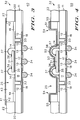
- FIG. 1 illustrates a partially cut-away top view of a portion 10 of a semiconductor device during processing in accordance with an embodiment of the present invention.
- Portion 10 of the semiconductor device comprises a substrate 11 having conductive traces 12 and bonding pads 13 disposed on the bottom surface and conductive traces 14 and chip or die attach pads 17 disposed on a top surface.
- Chip attach pads 17 serve as semiconductor chip receiving areas.
- conductive traces 12 and 14, bonding pads 13, and chip attach pads 17 are formed by laminating conductive foil to the top and bottom surfaces of substrate 11.
- Conductive traces 12 and 14, bonding pads 13, and chip attach pads 17 are defined by patterning the conductive foil using lithographic techniques.
- conductive traces 12 and 14, bonding pads 13, and chip attach pads 17 may be screen printed or otherwise deposited onto surfaces of the substrate. Subsequently, conductive traces 12 and 14, bonding pads 13, and chip attach pads 17 are typically plated with gold or a combination of gold and nickel to form a non-oxidizable surface for wirebonding and attaching solder balls 34 (shown in FIGs. 2-4). Although conductive traces 12 and 14, bonding pads 13, and chip attach pads 17 have been described as comprising two conductive layers, it should be understood that the number of conductive layers and the materials of the conductive layers is not a limitation of the present. It should be further understood that for purposes of clarity conductive traces 12 and 14, bonding pads 13, and chip attach pads 17 are illustrated in FIGs. 2-4 as being a single layer of material throughout the description of the invention.
- Conductive vias 33 are typically formed in substrate 11 by drilling or punching holes through the substrate and subsequently plating the holes with a conductive material such as, for example, copper.
- a conductive material such as, for example, copper.
- suitable materials for plating the holes include gold, nickel, a combination of gold and nickel, and the like.
- solder mask material 18 The bottom surface, including conductive traces 12 and bonding pads 13, is covered with a layer of solder mask material 18. Likewise, portions of the top surface, including conductive traces 14 and chip attach pads 17, are covered with a layer of solder mask material 19. Suitable solder mask materials include polyimide, high temperature epoxy resins, and the like. Openings or holes (not shown) are formed in solder mask material 18 to expose bonding pads 13, and openings (not shown) are formed in solder mask material 19 to expose chip attach pads 17 and portions of conductive traces 14. Methods for forming conductive traces, bonding pads, chip attach pads, and layers of solder mask material on a substrate are well known to those skilled in the art.
- a substrate support 22 having openings or apertures 23 is attached to the top surface of substrate 11. Chip attach pads 17 are exposed through openings 23 when substrate support 22 is attached to the top surface of substrate 11. In other words, substrate support 22 cooperates with substrate 11 to form cavities 25.
- Substrate support 22 is preferably formed from a resin, such as epoxy, polyimide, triazine, or a phenolic resin. More specifically, a bismaleimidetriazine (BT) resin is preferred.
- BT bismaleimidetriazine
- Other suitable materials for substrate support 22 include epoxy-glass composites, printed circuit board (PCB) materials, FR-4, ceramics, and the like. It should be understood that substrate support 22 is an electrically inert substrate, i.e., electrical circuitry is absent from substrate support 22.
- Substrate support 22 may be attached to substrate 11 by a thermosetting adhesive 20 (FIGs. 2-4) having a low curing temperature such as, for example, Ablebond TM 84-1A, manufactured by Ablestik Laboratories of Rancho Dominguez, California.
- Substrate support 22 serves as a stiffener to maintain the planarity of substrate 11 and to form walls surrounding chip attach pads 14 and 17, i.e., cavities 25.
- substrate support 22 preferably has a thickness ranging between approximately 125 microns ( ⁇ m) and approximately 1,250 ⁇ m.
- the thickness of substrate support 22 is not a limitation of the present invention; however, substrate support 22 should be of sufficient thickness so that interconnect wires 37 (FIGs. 2-4) may be covered by an encapsulant filling cavities 25.
- FIG. 1 further illustrates that substrate support 22 is a unitary structure having apertures 23 that form cavities 25 when it is coupled to substrate 11.
- FIG. 2 a highly enlarged cross-sectional view of a first embodiment of a semiconductor device 30 is shown, wherein semiconductor device 30 comprises a semiconductor chip 31 coupled to a BGA package 32.
- BGA package 32 includes substrate 11 having conductive traces 12 and bonding pads 13 on a bottom surface and conductive traces 14 and a die attach pad 17 on a top surface.
- Each conductive trace 14 on the top surface is coupled to a corresponding conductive trace 12 on the bottom surface by conductive vias 33.
- conductive vias 33 Although the inner portions of conductive vias 33 are shown as being hollow, it should understood that this is not a limitation of the present invention and that conductive vias 33 may be filled with a conductive material.
- Semiconductor device 30 further includes solder mask layers 18 and 19.
- Solder balls 34 are coupled to bonding pads 13 by positioning each solder ball 34 on a corresponding bonding pad 13 in the presence of a flux and performing a solder reflow operation to form a metallurgical bond.
- Techniques for coupling solder balls to bonding pads are well known in the art.
- U.S. Patent No. 5,284,287 entitled “METHOD FOR ATTACHING CONDUCTIVE BALLS TO A SUBSTRATE” issued to Wilson et al., assigned to the same assignee, Motorola, Inc. and which is hereby incorporated herein by reference teaches a method for coupling a solder ball to a bonding pad. It should be understood that the embodiment illustrated in FIG.
- solder balls 34 are coupled to bonding pads 13.
- BGA ball grid array
- PGA pin grid array
- LGA land grid array
- Semiconductor chip 31 is coupled to chip attach pad 17 via a die attach material 35 such as, for example, a silver filled epoxy.
- die attach material 35 such as, for example, a silver filled epoxy.
- suitable die attach materials include rubbers, silicones, polyurethanes, and thermoplastics.
- Chip bond pads 36 are coupled to corresponding conductive traces 14 via interconnect wires 37. Techniques for coupling semiconductor chips to chip attach pads and wirebonding chip bond pads with conductive traces are well known to those skilled in the art.
- semiconductor die 31 is covered with an encapsulating material 38. More particularly, encapsulating material 38 fills cavity 25 formed by coupling substrate support 22 to substrate 11. Suitable materials for encapsulating material 38 include a high purity, low stress, liquid encapsulant sold under the trademark Hysol FP4450 or a high purity, liquid epoxy encapsulant sold under the trademark Hysol CNB 648-48 or Hysol CNB 650-51. Preferably, encapsulating material 38 is selected to have a coefficient of thermal expansion that matches the coefficient of thermal expansion of semiconductor chip 31.
- the amount of encapsulating material 38 in contact with semiconductor chip 31 is greater than the amount of encapsulating material 38 in contact with substrate 11.
- An advantage of matching the coefficients of thermal expansion of encapsulating material 38 and semiconductor chip 31 is that it prevents breakage of wires in contact with semiconductor chip 31.
- encapsulating material 38 protects semiconductor chip 31 from moisture, mechanical stresses, contamination, conductive debris, alpha emissions, etc.
- FIG. 3 illustrates a highly enlarged cross-sectional view of a semiconductor device 40 in accordance with a second embodiment of the present invention.
- Semiconductor device 40 comprises a semiconductor chip 31 coupled to an BGA package 32, wherein semiconductor chip 31 is within cavity 25.
- cavity 25 is filled with a fluid 43 and covered with a cap 41.
- fluid 43 is an inert, high-dielectric, thermally conductive material such as silicone.
- Cap 41 is bonded to semiconductor support 22 using an adhesive material 42. Suitable materials for cap 41 include metal, plastic, and ceramic materials.
- a suitable material for adhesive material 42 is a thermosetting adhesive having a low curing temperature such as, for example, Ablebond TM 84-1A, manufactured by Ablestik Laboratories of Rancho Dominguez, California. Similar to encapsulating material 38 described with reference to FIG. 2, cap 41 covers and protects semiconductor chip 31 from moisture, mechanical stresses, contamination, conductive debris, alpha emissions, etc. Further, it is preferable that the material of cap 41 is selected such that its coefficient of thermal expansion matches that of substrate support 22. Although cavity 25 is shown as being filled with fluid 43, it should be understood that filling cavity 25 with fluid 43 is optional.
- FIG. 4 illustrates a highly enlarged cross-sectional view of a semiconductor device 50 in accordance with a third embodiment of the present invention.
- Semiconductor device 50 comprises a semiconductor chip 31 coupled to a BGA package 32, wherein semiconductor chip 31 is within cavity 25. A portion of cavity 25 is covered with a cap 51.
- cap 51 is bonded to substrate support 22 by an adhesive material 55. More particularly, cap 51 comprises a coined sheet of metal having a raised portion 52 surrounding a central depression 53 and a cap support 54 for bonding to substrate support 22.
- cap 51 is formed to have a portion contoured to the shape of substrate support 22, i.e., cap support 54, a portion contoured to the shape of interconnect wires 37, i.e., raised portion 52, and a portion contoured to the shape the surface of semiconductor chip 31, i.e., central depression 53. It should be understood that cap 51 is electrically isolated from interconnect wires 37.
- cap 51 is selected such that it's coefficient of thermal expansion matches that of substrate support 22.
- the inductance of interconnect wires 37 and the resonant frequency of semiconductor device 50 can be optimized by forming cap 51 as a bi-metal laminated cap comprising a layer of iron 56 and a layer of aluminum 57.
- iron layer 56 has a thickness of approximately 150 ⁇ m and aluminum layer 57 has a thickness of approximately 450 ⁇ m.
- layer of iron 56 faces semiconductor chip 31.
- the semiconductor device includes a substrate support mounted to a thin substrate having conductive traces formed thereon.
- the substrate support provides structural strength and serves as a stiffener for the thin substrate.
- the substrate support prevents the thin substrate from warping and permits use of thin substrates.
- the thin substrate having conductive traces may be as thin as a TAB (tape automated bonded) tape, allowing the thin substrate having conductive traces to be processed in rolls.
- TAB tape automated bonded
- Another advantage of the substrate support of the present invention is that it eliminates the steps of forming dams around each semiconductor chip receiving area. Typically, dam formation requires a large amount of encapsulating material.
- Another advantage of a thin substrate having conductive traces formed thereon is that the thin substrate facilitates cancellation of inductances of traces on opposing sides of the thin substrate.
- the present invention decreases the cost of manufacturing semiconductor devices. Further, the dams of GTPAC semiconductor devices are made in a sequential fashion, adding to the overall time required to manufacture the semiconductor devices. Since the present invention eliminates dam formation, the cost of materials is reduced and the cycle times for forming the semiconductor devices is decreased. As those skilled in the art are aware, eliminating processing steps inherently results in an increase in yields.
- the substrate support may be mounted to multi-layer substrates.
Abstract
Description
- The present invention relates, in general, to semiconductor devices, and more particularly, to semiconductor device packages.
- Semiconductor device manufacturers are constantly striving to lower the cost of manufacturing semiconductor devices while improving device electrical and thermal performance characteristics. In addition, it is desirable for the devices to be small, light weight, and have a low profile. Thus, over-molded pad array carrier (OMPAC) semiconductor devices have been developed to improve both the electrical and thermal performance of surface mount semiconductor devices. Typically, OMPAC semiconductor devices include a thin printed circuit board (PCB) substrate on which a semiconductor chip is mounted. Portions of the chip are electrically coupled to conductive traces formed on a top surface of the PCB. Each conductive trace is routed to a corresponding conductive trace on the bottom surface of the PCB by a conductive via which extends through the PCB. The traces on the bottom surface of the PCB each terminate at a conductive pad to form an array of pads on the bottom of the PCB. The semiconductor chip and a portion of the PCB are encapsulated by a molding compound using conventional molding techniques, i.e., placing the PCB having the semiconductor chip mounted thereon in a mold cavity, converting a mold compound from a pellet form to a liquid form, injecting the liquid mold compound into the mold cavity, and curing the mold compound. Although OMPAC semiconductor devices offer the advantages of increased interconnect packaging densities, elimination of coplanarity and skew limitations, low lead inductance, and a low profile, they require a different mold for each type of OMPAC semiconductor device. Since these molds are expensive, manufacturing different types of semiconductor devices is also expensive. In addition, the cost of maintaining molding equipment is high. Further, the mold compounds used in manufacturing OMPAC semiconductor devices require extensive cure times which result in increased cycle times.
- Another type of surface mount semiconductor device is a glob-top pad array carrier (GTPAC) semiconductor device. A GTPAC semiconductor device comprises a PCB having a semiconductor chip mounted thereon and a wall or dam of thixotropic material formed on the PCB. The dam surrounds and is spaced apart from the semiconductor chip. Subsequently, the semiconductor chip and the portion of the PCB within the dam are covered by a liquid encapsulant. The dam and the encapsulant form a package body. Although, GTPAC semiconductor packages may offer an increased electrical performance over conventional surface mount packages, they require a thicker PCB to preclude planarity limitations. In addition, the dam material is difficult to dispense and increases cycle time, resulting in higher manufacturing costs.
- Accordingly, it would be advantageous to have a method and a means for encapsulating semiconductor chips that does not limit the thickness of the PCB and is readily incorporated into existing manufacturing processes. It would be of further advantage for the method and means to reduce the cost and time required to manufacture semiconductor devices. In addition, it would be advantageous for the method and means to improve the electrical and thermal performance of the semiconductor device.
-
- FIG. 1 illustrates a partially cut-away top view of a portion of a semiconductor device during processing in accordance with an embodiment of the present invention;
- FIG. 2 illustrates a highly enlarged cross-sectional view of a portion of a semiconductor device in accordance with a first embodiment of the present invention;
- FIG. 3 illustrates a highly enlarged cross-sectional view of a portion of a semiconductor device in accordance with a second embodiment of the present invention; and
- FIG. 4 illustrates a highly enlarged cross-sectional view of a portion of a semiconductor device in accordance with a third embodiment of the present invention.
- Generally, the present invention provides a method and a means for encapsulating a semiconductor chip in a recessed ball grid array (BGA) package. In accordance with the present invention, a substrate support having a plurality of apertures is mounted or laminated to a substrate having a plurality of semiconductor chip receiving areas. The substrate support prevents the substrate from warping thereby permitting the use of thin substrates. As those skilled in the art will appreciate, thinner substrates improve the electrical performance of semiconductor devices. A nominal thickness range of substrate used in accordance with the present invention is between approximately 50 microns (µm) and approximately 1,500 µm. A semiconductor chip is mounted in each semiconductor chip receiving area and the semiconductor chip is covered. Subsequently, the substrate having the substrate support and the semiconductor chips mounted thereto is singulated into individual semiconductor devices. Techniques for forming individual semiconductor devices are well known and include, for example, cutting, sawing, punching, or the like.
- FIG. 1 illustrates a partially cut-away top view of a
portion 10 of a semiconductor device during processing in accordance with an embodiment of the present invention.Portion 10 of the semiconductor device comprises asubstrate 11 havingconductive traces 12 andbonding pads 13 disposed on the bottom surface andconductive traces 14 and chip ordie attach pads 17 disposed on a top surface.Chip attach pads 17 serve as semiconductor chip receiving areas. By way of example,conductive traces pads 13, andchip attach pads 17 are formed by laminating conductive foil to the top and bottom surfaces ofsubstrate 11.Conductive traces bonding pads 13, andchip attach pads 17 are defined by patterning the conductive foil using lithographic techniques. Alternatively,conductive traces bonding pads 13, andchip attach pads 17 may be screen printed or otherwise deposited onto surfaces of the substrate. Subsequently,conductive traces pads 13, andchip attach pads 17 are typically plated with gold or a combination of gold and nickel to form a non-oxidizable surface for wirebonding and attaching solder balls 34 (shown in FIGs. 2-4). Althoughconductive traces bonding pads 13, andchip attach pads 17 have been described as comprising two conductive layers, it should be understood that the number of conductive layers and the materials of the conductive layers is not a limitation of the present. It should be further understood that for purposes of clarityconductive traces pads 13, andchip attach pads 17 are illustrated in FIGs. 2-4 as being a single layer of material throughout the description of the invention. -
Conductive vias 33 are typically formed insubstrate 11 by drilling or punching holes through the substrate and subsequently plating the holes with a conductive material such as, for example, copper. Other suitable materials for plating the holes include gold, nickel, a combination of gold and nickel, and the like. Thus, only the sidewalls of the holes or vias are conductive, whereas the inner portions are hollow. - The bottom surface, including
conductive traces 12 and bondingpads 13, is covered with a layer ofsolder mask material 18. Likewise, portions of the top surface, includingconductive traces 14 andchip attach pads 17, are covered with a layer ofsolder mask material 19. Suitable solder mask materials include polyimide, high temperature epoxy resins, and the like. Openings or holes (not shown) are formed insolder mask material 18 to exposebonding pads 13, and openings (not shown) are formed insolder mask material 19 to exposechip attach pads 17 and portions ofconductive traces 14. Methods for forming conductive traces, bonding pads, chip attach pads, and layers of solder mask material on a substrate are well known to those skilled in the art. - A
substrate support 22 having openings orapertures 23 is attached to the top surface ofsubstrate 11.Chip attach pads 17 are exposed throughopenings 23 whensubstrate support 22 is attached to the top surface ofsubstrate 11. In other words, substrate support 22 cooperates withsubstrate 11 to formcavities 25.Substrate support 22 is preferably formed from a resin, such as epoxy, polyimide, triazine, or a phenolic resin. More specifically, a bismaleimidetriazine (BT) resin is preferred. Other suitable materials forsubstrate support 22 include epoxy-glass composites, printed circuit board (PCB) materials, FR-4, ceramics, and the like. It should be understood thatsubstrate support 22 is an electrically inert substrate, i.e., electrical circuitry is absent fromsubstrate support 22.Substrate support 22 may be attached tosubstrate 11 by a thermosetting adhesive 20 (FIGs. 2-4) having a low curing temperature such as, for example, Ablebond TM 84-1A, manufactured by Ablestik Laboratories of Rancho Dominguez, California.Substrate support 22 serves as a stiffener to maintain the planarity ofsubstrate 11 and to form walls surroundingchip attach pads cavities 25. Accordingly,substrate support 22 preferably has a thickness ranging between approximately 125 microns (µm) and approximately 1,250 µm. Although, it should be understood that the thickness ofsubstrate support 22 is not a limitation of the present invention; however,substrate support 22 should be of sufficient thickness so that interconnect wires 37 (FIGs. 2-4) may be covered by anencapsulant filling cavities 25. - FIG. 1 further illustrates that
substrate support 22 is a unitarystructure having apertures 23 that formcavities 25 when it is coupled tosubstrate 11. - Now referring to FIG. 2, a highly enlarged cross-sectional view of a first embodiment of a
semiconductor device 30 is shown, whereinsemiconductor device 30 comprises asemiconductor chip 31 coupled to aBGA package 32. It should be understood that the same reference numerals are used in the figures to denote the same elements.BGA package 32 includessubstrate 11 having conductive traces 12 andbonding pads 13 on a bottom surface andconductive traces 14 and a die attachpad 17 on a top surface. Eachconductive trace 14 on the top surface is coupled to a correspondingconductive trace 12 on the bottom surface byconductive vias 33. Although the inner portions ofconductive vias 33 are shown as being hollow, it should understood that this is not a limitation of the present invention and thatconductive vias 33 may be filled with a conductive material.Semiconductor device 30 further includes solder mask layers 18 and 19. -
Solder balls 34 are coupled tobonding pads 13 by positioning eachsolder ball 34 on acorresponding bonding pad 13 in the presence of a flux and performing a solder reflow operation to form a metallurgical bond. Techniques for coupling solder balls to bonding pads are well known in the art. For example, U.S. Patent No. 5,284,287 entitled "METHOD FOR ATTACHING CONDUCTIVE BALLS TO A SUBSTRATE" issued to Wilson et al., assigned to the same assignee, Motorola, Inc. and which is hereby incorporated herein by reference, teaches a method for coupling a solder ball to a bonding pad. It should be understood that the embodiment illustrated in FIG. 2 is also referred to as a ball grid array (BGA) becausesolder balls 34 are coupled tobonding pads 13. It should be further understood that the present invention is not limited to havingsolder balls 34 attached tobonding pads 13. For example, pin grid array (PGA) devices can be formed by attaching pins tobonding pads 13 and land grid array (LGA) devices can be formed by forming silver pads onbonding pads 13. -
Semiconductor chip 31 is coupled to chip attachpad 17 via a die attachmaterial 35 such as, for example, a silver filled epoxy. Other suitable die attach materials include rubbers, silicones, polyurethanes, and thermoplastics.Chip bond pads 36 are coupled to corresponding conductive traces 14 viainterconnect wires 37. Techniques for coupling semiconductor chips to chip attach pads and wirebonding chip bond pads with conductive traces are well known to those skilled in the art. - In accordance with the first embodiment of the present invention, semiconductor die 31 is covered with an encapsulating
material 38. More particularly, encapsulatingmaterial 38fills cavity 25 formed bycoupling substrate support 22 tosubstrate 11. Suitable materials for encapsulatingmaterial 38 include a high purity, low stress, liquid encapsulant sold under the trademark Hysol FP4450 or a high purity, liquid epoxy encapsulant sold under the trademark Hysol CNB 648-48 or Hysol CNB 650-51. Preferably, encapsulatingmaterial 38 is selected to have a coefficient of thermal expansion that matches the coefficient of thermal expansion ofsemiconductor chip 31. It should be noted that in accordance with the present invention the amount of encapsulatingmaterial 38 in contact withsemiconductor chip 31 is greater than the amount of encapsulatingmaterial 38 in contact withsubstrate 11. Thus, to lower thermally induced stresses onsemiconductor chip 31, it is desirable to match the coefficient of thermal expansion of encapsulatingmaterial 38 tosemiconductor chip 31 than tosubstrate 11. An advantage of matching the coefficients of thermal expansion of encapsulatingmaterial 38 andsemiconductor chip 31 is that it prevents breakage of wires in contact withsemiconductor chip 31. - It should be noted that encapsulating
material 38 protectssemiconductor chip 31 from moisture, mechanical stresses, contamination, conductive debris, alpha emissions, etc. - FIG. 3 illustrates a highly enlarged cross-sectional view of a
semiconductor device 40 in accordance with a second embodiment of the present invention.Semiconductor device 40 comprises asemiconductor chip 31 coupled to anBGA package 32, whereinsemiconductor chip 31 is withincavity 25. In accordance with the second embodiment,cavity 25 is filled with a fluid 43 and covered with acap 41. Preferably fluid 43 is an inert, high-dielectric, thermally conductive material such as silicone.Cap 41 is bonded tosemiconductor support 22 using anadhesive material 42. Suitable materials forcap 41 include metal, plastic, and ceramic materials. A suitable material foradhesive material 42 is a thermosetting adhesive having a low curing temperature such as, for example, Ablebond TM 84-1A, manufactured by Ablestik Laboratories of Rancho Dominguez, California. Similar to encapsulatingmaterial 38 described with reference to FIG. 2, cap 41 covers and protectssemiconductor chip 31 from moisture, mechanical stresses, contamination, conductive debris, alpha emissions, etc. Further, it is preferable that the material ofcap 41 is selected such that its coefficient of thermal expansion matches that ofsubstrate support 22. Althoughcavity 25 is shown as being filled withfluid 43, it should be understood that fillingcavity 25 withfluid 43 is optional. - FIG. 4 illustrates a highly enlarged cross-sectional view of a
semiconductor device 50 in accordance with a third embodiment of the present invention.Semiconductor device 50 comprises asemiconductor chip 31 coupled to aBGA package 32, whereinsemiconductor chip 31 is withincavity 25. A portion ofcavity 25 is covered with acap 51. By way of example,cap 51 is bonded tosubstrate support 22 by anadhesive material 55. More particularly,cap 51 comprises a coined sheet of metal having a raised portion 52 surrounding acentral depression 53 and acap support 54 for bonding tosubstrate support 22. In other words, cap 51 is formed to have a portion contoured to the shape ofsubstrate support 22, i.e.,cap support 54, a portion contoured to the shape ofinterconnect wires 37, i.e., raised portion 52, and a portion contoured to the shape the surface ofsemiconductor chip 31, i.e.,central depression 53. It should be understood thatcap 51 is electrically isolated frominterconnect wires 37. - Preferably, the material of
cap 51 is selected such that it's coefficient of thermal expansion matches that ofsubstrate support 22. Further, the inductance ofinterconnect wires 37 and the resonant frequency ofsemiconductor device 50 can be optimized by formingcap 51 as a bi-metal laminated cap comprising a layer of iron 56 and a layer ofaluminum 57. By way of example, iron layer 56 has a thickness of approximately 150 µm andaluminum layer 57 has a thickness of approximately 450 µm. Preferably, layer of iron 56 facessemiconductor chip 31. - By now it should be appreciated that a method and a means have been provided for forming a semiconductor device. The semiconductor device includes a substrate support mounted to a thin substrate having conductive traces formed thereon. The substrate support provides structural strength and serves as a stiffener for the thin substrate. Thus, the substrate support prevents the thin substrate from warping and permits use of thin substrates. For example, the thin substrate having conductive traces may be as thin as a TAB (tape automated bonded) tape, allowing the thin substrate having conductive traces to be processed in rolls. Another advantage of the substrate support of the present invention is that it eliminates the steps of forming dams around each semiconductor chip receiving area. Typically, dam formation requires a large amount of encapsulating material. Another advantage of a thin substrate having conductive traces formed thereon is that the thin substrate facilitates cancellation of inductances of traces on opposing sides of the thin substrate.
- Since the encapsulating material is much more expensive than the material used in forming the substrate support, the present invention decreases the cost of manufacturing semiconductor devices. Further, the dams of GTPAC semiconductor devices are made in a sequential fashion, adding to the overall time required to manufacture the semiconductor devices. Since the present invention eliminates dam formation, the cost of materials is reduced and the cycle times for forming the semiconductor devices is decreased. As those skilled in the art are aware, eliminating processing steps inherently results in an increase in yields.
- While specific embodiments of the invention have been shown and described, further modifications and improvements will occur to those skilled in the art. It is understood that this invention is not limited to the particular forms shown and it is intended for the appended claims to cover all modifications of the invention which fall within the true spirit and scope of the invention. For example, the substrate support may be mounted to multi-layer substrates.
Claims (10)
- A semiconductor chip package, comprising: a substrate (11) having a semiconductor chip receiving area (17); and
a substrate support (22) coupled to the substrate (11), the substrate support (22) having an aperture (23) exposing the semiconductor chip receiving area (17), wherein the aperture (23) cooperates with the substrate (11) to form a cavity (25). - The semiconductor chip package of claim 1, wherein a semiconductor chip (31) is coupled to the semiconductor chip receiving area (17) and interconnect wires (37) are bonded to the semiconductor chip (31) and the cavity (25) is covered with a metal cap having a portion that conforms to the shape of the interconnect wires (37) and is electrically separated from the interconnect wires (37).
- The semiconductor chip package of claim 1, wherein the cavity (25) is covered by a cap (41).
- The semiconductor chip package of claim 3, wherein a material of the cap (41) is a bi-metal laminated cap comprising a layer of aluminum and a layer of iron.
- The semiconductor chip package of claim 1, wherein a thickness of the substrate support (22) ranges between approximately 125 microns and approximately 1,250 microns.
- A semiconductor device package, comprising:
a substrate (11) having top and bottom surfaces, wherein the top surface has a semiconductor chip attach pad (17) formed thereon and the bottom surface has a bonding pad (13) formed thereon;
a semiconductor chip (31) mounted to the semiconductor chip attach pad (17); and
a substrate support (22) coupled to the top surface, wherein the substrate support (22) has an aperture (23), the semiconductor chip (31) exposed through the aperture (23) and the aperture (23) forming a cavity (25). - The semiconductor device package of claim 6, wherein a solder ball (34) is bonded to the bonding pad (13) on the bottom surface.
- The semiconductor device package of claim 6, wherein an encapsulating material (38) fills the cavity (25).
- A method for forming a semiconductor device package, comprising the steps of:
providing a substrate (11) having a die bonding area (17); and
attaching a support (22) to the substrate (11), the support (22) having an aperture (23) aligned to and exposing the die bonding area (17). - The method of claim 9, wherein the step of attaching a support (22) to the substrate (11) includes mounting a semiconductor chip (31) to the die bonding area (17) and covering the semiconductor chip (31) with an encapsulation material (38).
Applications Claiming Priority (2)
| Application Number | Priority Date | Filing Date | Title |
|---|---|---|---|
| US08/269,241 US5467253A (en) | 1994-06-30 | 1994-06-30 | Semiconductor chip package and method of forming |
| US269241 | 1994-06-30 |
Publications (3)
| Publication Number | Publication Date |
|---|---|
| EP0690497A2 true EP0690497A2 (en) | 1996-01-03 |
| EP0690497A3 EP0690497A3 (en) | 1997-06-11 |
| EP0690497B1 EP0690497B1 (en) | 2002-05-02 |
Family
ID=23026421
Family Applications (1)
| Application Number | Title | Priority Date | Filing Date |
|---|---|---|---|
| EP95109712A Expired - Lifetime EP0690497B1 (en) | 1994-06-30 | 1995-06-22 | Semiconductor device and method of forming |
Country Status (4)
| Country | Link |
|---|---|
| US (1) | US5467253A (en) |
| EP (1) | EP0690497B1 (en) |
| JP (1) | JP3466785B2 (en) |
| DE (1) | DE69526539T2 (en) |
Families Citing this family (50)
| Publication number | Priority date | Publication date | Assignee | Title |
|---|---|---|---|---|
| US5457878A (en) * | 1993-10-12 | 1995-10-17 | Lsi Logic Corporation | Method for mounting integrated circuit chips on a mini-board |
| KR100648751B1 (en) * | 1994-05-02 | 2007-03-02 | 지멘스 마츠시타 컴포넌츠 게엠베하 운트 콤파니 카게 | Sealing device for electronic parts |
| US6465743B1 (en) * | 1994-12-05 | 2002-10-15 | Motorola, Inc. | Multi-strand substrate for ball-grid array assemblies and method |
| JP3201187B2 (en) * | 1994-12-08 | 2001-08-20 | 富士電機株式会社 | Semiconductor device |
| US5605547A (en) * | 1995-03-27 | 1997-02-25 | Micron Technology, Inc. | Method and apparatus for mounting a component to a substrate using an anisotropic adhesive, a compressive cover film, and a conveyor |
| JP2679681B2 (en) * | 1995-04-28 | 1997-11-19 | 日本電気株式会社 | Semiconductor device, package for semiconductor device, and manufacturing method thereof |
| JP3060896B2 (en) * | 1995-05-26 | 2000-07-10 | 日本電気株式会社 | Structure of bump electrode |
| KR100386061B1 (en) | 1995-10-24 | 2003-08-21 | 오끼 덴끼 고오교 가부시끼가이샤 | Semiconductor device and lead frame with improved construction to prevent cracking |
| US5731709A (en) * | 1996-01-26 | 1998-03-24 | Motorola, Inc. | Method for testing a ball grid array semiconductor device and a device for such testing |
| JPH09222372A (en) * | 1996-02-19 | 1997-08-26 | Mitsubishi Electric Corp | Semiconductor sensor |
| US7166495B2 (en) * | 1996-02-20 | 2007-01-23 | Micron Technology, Inc. | Method of fabricating a multi-die semiconductor package assembly |
| US5696031A (en) * | 1996-11-20 | 1997-12-09 | Micron Technology, Inc. | Device and method for stacking wire-bonded integrated circuit dice on flip-chip bonded integrated circuit dice |
| US5771157A (en) * | 1996-03-08 | 1998-06-23 | Honeywell, Inc. | Chip-on-board printed circuit assembly using aluminum wire bonded to copper pads |
| KR100206894B1 (en) * | 1996-03-11 | 1999-07-01 | 구본준 | Bga package |
| US5776798A (en) * | 1996-09-04 | 1998-07-07 | Motorola, Inc. | Semiconductor package and method thereof |
| US5789813A (en) * | 1996-09-30 | 1998-08-04 | Lsi Logic Corporation | Ball grid array package with inexpensive threaded secure locking mechanism to allow removal of a threaded heat sink therefrom |
| US5847445A (en) * | 1996-11-04 | 1998-12-08 | Micron Technology, Inc. | Die assemblies using suspended bond wires, carrier substrates and dice having wire suspension structures, and methods of fabricating same |
| US6429387B1 (en) * | 1996-12-13 | 2002-08-06 | Matsushita Electric Industrial Co., Ltd. | Electronic component and mounting method and device therefor |
| US6064116A (en) * | 1997-06-06 | 2000-05-16 | Micron Technology, Inc. | Device for electrically or thermally coupling to the backsides of integrated circuit dice in chip-on-board applications |
| US5923959A (en) | 1997-07-23 | 1999-07-13 | Micron Technology, Inc. | Ball grid array (BGA) encapsulation mold |
| US6472252B2 (en) * | 1997-07-23 | 2002-10-29 | Micron Technology, Inc. | Methods for ball grid array (BGA) encapsulation mold |
| JP3669463B2 (en) * | 1997-08-05 | 2005-07-06 | Tdk株式会社 | Resin-encapsulated surface-mount electronic components |
| US5972734A (en) * | 1997-09-17 | 1999-10-26 | Lsi Logic Corporation | Interposer for ball grid array (BGA) package |
| US6284570B1 (en) | 1998-12-28 | 2001-09-04 | Semiconductor Components Industries Llc | Method of manufacturing a semiconductor component from a conductive substrate containing a plurality of vias |
| KR100319609B1 (en) | 1999-03-09 | 2002-01-05 | 김영환 | A wire arrayed chip size package and the fabrication method thereof |
| DE19964316B4 (en) * | 1999-03-30 | 2006-11-23 | Mitsubishi Denki K.K. | Semiconductor device manufacturing method for e.g. GaAs FET involves sticking chips to substrate, sticking lid to substrate and separating chips along adjoining areas |
| JP3408987B2 (en) * | 1999-03-30 | 2003-05-19 | 三菱電機株式会社 | Semiconductor device manufacturing method and semiconductor device |
| US6495916B1 (en) * | 1999-04-06 | 2002-12-17 | Oki Electric Industry Co., Ltd. | Resin-encapsulated semiconductor device |
| US6281096B1 (en) | 1999-04-22 | 2001-08-28 | International Rectifier Corp. | Chip scale packaging process |
| JP4190111B2 (en) * | 1999-10-29 | 2008-12-03 | 富士通株式会社 | High frequency module |
| US6830462B1 (en) | 1999-12-13 | 2004-12-14 | Fci Americas Technology, Inc. | Electrical connector housing |
| EP1240808B1 (en) * | 1999-12-17 | 2003-05-21 | Osram Opto Semiconductors GmbH | Encapsulation for organic led device |
| US7394153B2 (en) * | 1999-12-17 | 2008-07-01 | Osram Opto Semiconductors Gmbh | Encapsulation of electronic devices |
| TW493262B (en) | 2000-02-10 | 2002-07-01 | Int Rectifier Corp | Vertical conduction flip-chip device with bump contacts on single surface |
| DE10014380A1 (en) | 2000-03-23 | 2001-10-04 | Infineon Technologies Ag | Device for packaging electronic components |
| US6431432B1 (en) * | 2000-06-15 | 2002-08-13 | Lsi Logic Corporation | Method for attaching solderballs by selectively oxidizing traces |
| US6570271B2 (en) * | 2001-05-16 | 2003-05-27 | Hewlett-Packard Development Company, L.P. | Apparatus for routing signals |
| US6528892B2 (en) | 2001-06-05 | 2003-03-04 | International Business Machines Corporation | Land grid array stiffener use with flexible chip carriers |
| US7245500B2 (en) * | 2002-02-01 | 2007-07-17 | Broadcom Corporation | Ball grid array package with stepped stiffener layer |
| JP2003249743A (en) * | 2002-02-26 | 2003-09-05 | Seiko Epson Corp | Wiring substrate and method of manufacturing the same, semiconductor device and electronic device |
| JP3701949B2 (en) * | 2003-04-16 | 2005-10-05 | 沖電気工業株式会社 | Wiring board for mounting semiconductor chip and manufacturing method thereof |
| JP2005311118A (en) * | 2004-04-22 | 2005-11-04 | Seiko Epson Corp | Semiconductor device and its manufacturing method, electro-optical device, and electronic apparatus |
| TWI300679B (en) * | 2006-02-22 | 2008-09-01 | Au Optronics Corp | Assembly of fpc and electric component |
| US7768075B2 (en) | 2006-04-06 | 2010-08-03 | Fairchild Semiconductor Corporation | Semiconductor die packages using thin dies and metal substrates |
| US20080123335A1 (en) * | 2006-11-08 | 2008-05-29 | Jong Kun Yoo | Printed circuit board assembly and display having the same |
| US8159828B2 (en) * | 2007-02-23 | 2012-04-17 | Alpha & Omega Semiconductor, Inc. | Low profile flip chip power module and method of making |
| US20120314390A1 (en) * | 2010-03-03 | 2012-12-13 | Mutual-Tek Industries Co., Ltd. | Multilayer circuit board |
| DE102011088256A1 (en) * | 2011-12-12 | 2013-06-13 | Zf Friedrichshafen Ag | Multilayer printed circuit board and arrangement with such |
| US9070653B2 (en) | 2013-01-15 | 2015-06-30 | Freescale Semiconductor, Inc. | Microelectronic assembly having a heat spreader for a plurality of die |
| JP2018147938A (en) * | 2017-03-01 | 2018-09-20 | 東芝メモリ株式会社 | Semiconductor device |
Citations (1)
| Publication number | Priority date | Publication date | Assignee | Title |
|---|---|---|---|---|
| US5284287A (en) | 1992-08-31 | 1994-02-08 | Motorola, Inc. | Method for attaching conductive balls to a substrate |
Family Cites Families (11)
| Publication number | Priority date | Publication date | Assignee | Title |
|---|---|---|---|---|
| US4524238A (en) * | 1982-12-29 | 1985-06-18 | Olin Corporation | Semiconductor packages |
| JPS62194648A (en) * | 1986-02-21 | 1987-08-27 | Hitachi Ltd | Glass package type electronic device |
| JPH01102757A (en) * | 1987-10-14 | 1989-04-20 | Ricoh Co Ltd | Magneto-optical recording medium |
| JPH02202040A (en) * | 1989-01-31 | 1990-08-10 | Mitsubishi Electric Corp | Semiconductor device |
| US5173766A (en) * | 1990-06-25 | 1992-12-22 | Lsi Logic Corporation | Semiconductor device package and method of making such a package |
| WO1992020097A1 (en) * | 1991-04-26 | 1992-11-12 | Citizen Watch Co., Ltd. | Semiconductor device and manufacturing method therefor |
| US5278726A (en) * | 1992-01-22 | 1994-01-11 | Motorola, Inc. | Method and apparatus for partially overmolded integrated circuit package |
| JP3480950B2 (en) * | 1992-04-02 | 2003-12-22 | 新光電気工業株式会社 | Semiconductor device and film carrier for semiconductor device |
| EP0582052A1 (en) * | 1992-08-06 | 1994-02-09 | Motorola, Inc. | Low profile overmolded semiconductor device and method for making the same |
| US5355283A (en) * | 1993-04-14 | 1994-10-11 | Amkor Electronics, Inc. | Ball grid array with via interconnection |
| US5397917A (en) * | 1993-04-26 | 1995-03-14 | Motorola, Inc. | Semiconductor package capable of spreading heat |
-
1994
- 1994-06-30 US US08/269,241 patent/US5467253A/en not_active Expired - Lifetime
-
1995
- 1995-06-22 EP EP95109712A patent/EP0690497B1/en not_active Expired - Lifetime
- 1995-06-22 DE DE69526539T patent/DE69526539T2/en not_active Expired - Lifetime
- 1995-06-23 JP JP17960395A patent/JP3466785B2/en not_active Expired - Lifetime
Patent Citations (1)
| Publication number | Priority date | Publication date | Assignee | Title |
|---|---|---|---|---|
| US5284287A (en) | 1992-08-31 | 1994-02-08 | Motorola, Inc. | Method for attaching conductive balls to a substrate |
Also Published As
| Publication number | Publication date |
|---|---|
| DE69526539T2 (en) | 2002-11-07 |
| DE69526539D1 (en) | 2002-06-06 |
| EP0690497B1 (en) | 2002-05-02 |
| JP3466785B2 (en) | 2003-11-17 |
| JPH0817957A (en) | 1996-01-19 |
| EP0690497A3 (en) | 1997-06-11 |
| US5467253A (en) | 1995-11-14 |
Similar Documents
| Publication | Publication Date | Title |
|---|---|---|
| US5467253A (en) | Semiconductor chip package and method of forming | |
| US5397917A (en) | Semiconductor package capable of spreading heat | |
| EP1256980B1 (en) | Ball grid array package with a heat spreader and method for making the same | |
| US7679172B2 (en) | Semiconductor package without chip carrier and fabrication method thereof | |
| US8546183B2 (en) | Method for fabricating heat dissipating semiconductor package | |
| US6995448B2 (en) | Semiconductor package including passive elements and method of manufacture | |
| US6964888B2 (en) | Semiconductor device and method for fabricating the same | |
| US7102225B2 (en) | Die-up ball grid array package with printed circuit board attachable heat spreader | |
| US7138706B2 (en) | Semiconductor device and method for manufacturing the same | |
| US6856007B2 (en) | High-frequency chip packages | |
| US6599779B2 (en) | PBGA substrate for anchoring heat sink | |
| US8796561B1 (en) | Fan out build up substrate stackable package and method | |
| US8169067B2 (en) | Low profile ball grid array (BGA) package with exposed die and method of making same | |
| EP1119038A2 (en) | Method of producing a semiconductor device | |
| US20060292753A1 (en) | Semiconductor Device and Method of Manufacturing a Semiconductor Device | |
| AU647864B2 (en) | Leadless pad array chip carrier | |
| US6819565B2 (en) | Cavity-down ball grid array semiconductor package with heat spreader | |
| US7173341B2 (en) | High performance thermally enhanced package and method of fabricating the same | |
| US20040173903A1 (en) | Thin type ball grid array package | |
| US6794222B1 (en) | HDI module with integral conductive electromagnetic shield | |
| US20040021213A1 (en) | Thermally-enhanced integrated circuit package | |
| JPH06163760A (en) | Electronic-component mounting board provided with heat-dissipating slug |
Legal Events
| Date | Code | Title | Description |
|---|---|---|---|
| PUAI | Public reference made under article 153(3) epc to a published international application that has entered the european phase |
Free format text: ORIGINAL CODE: 0009012 |
|
| AK | Designated contracting states |
Kind code of ref document: A2 Designated state(s): DE FR GB |
|
| PUAL | Search report despatched |
Free format text: ORIGINAL CODE: 0009013 |
|
| AK | Designated contracting states |
Kind code of ref document: A3 Designated state(s): DE FR GB |
|
| 17P | Request for examination filed |
Effective date: 19971211 |
|
| 17Q | First examination report despatched |
Effective date: 19981222 |
|
| GRAG | Despatch of communication of intention to grant |
Free format text: ORIGINAL CODE: EPIDOS AGRA |
|
| GRAG | Despatch of communication of intention to grant |
Free format text: ORIGINAL CODE: EPIDOS AGRA |
|
| GRAH | Despatch of communication of intention to grant a patent |
Free format text: ORIGINAL CODE: EPIDOS IGRA |
|
| REG | Reference to a national code |
Ref country code: GB Ref legal event code: IF02 |
|
| GRAH | Despatch of communication of intention to grant a patent |
Free format text: ORIGINAL CODE: EPIDOS IGRA |
|
| GRAA | (expected) grant |
Free format text: ORIGINAL CODE: 0009210 |
|
| AK | Designated contracting states |
Kind code of ref document: B1 Designated state(s): DE FR GB |
|
| REG | Reference to a national code |
Ref country code: GB Ref legal event code: FG4D |
|
| REF | Corresponds to: |
Ref document number: 69526539 Country of ref document: DE Date of ref document: 20020606 |
|
| ET | Fr: translation filed | ||
| PLBE | No opposition filed within time limit |
Free format text: ORIGINAL CODE: 0009261 |
|
| STAA | Information on the status of an ep patent application or granted ep patent |
Free format text: STATUS: NO OPPOSITION FILED WITHIN TIME LIMIT |
|
| 26N | No opposition filed |
Effective date: 20030204 |
|
| REG | Reference to a national code |
Ref country code: GB Ref legal event code: 732E |
|
| REG | Reference to a national code |
Ref country code: FR Ref legal event code: TP |
|
| PGFP | Annual fee paid to national office [announced via postgrant information from national office to epo] |
Ref country code: GB Payment date: 20140627 Year of fee payment: 20 |
|
| PGFP | Annual fee paid to national office [announced via postgrant information from national office to epo] |
Ref country code: DE Payment date: 20140627 Year of fee payment: 20 |
|
| PGFP | Annual fee paid to national office [announced via postgrant information from national office to epo] |
Ref country code: FR Payment date: 20140617 Year of fee payment: 20 |
|
| REG | Reference to a national code |
Ref country code: DE Ref legal event code: R071 Ref document number: 69526539 Country of ref document: DE |
|
| REG | Reference to a national code |
Ref country code: GB Ref legal event code: PE20 Expiry date: 20150621 |
|
| PG25 | Lapsed in a contracting state [announced via postgrant information from national office to epo] |
Ref country code: GB Free format text: LAPSE BECAUSE OF EXPIRATION OF PROTECTION Effective date: 20150621 |