EP0684423A2 - Backlight device for display apparatus - Google Patents
Backlight device for display apparatus Download PDFInfo
- Publication number
- EP0684423A2 EP0684423A2 EP95303585A EP95303585A EP0684423A2 EP 0684423 A2 EP0684423 A2 EP 0684423A2 EP 95303585 A EP95303585 A EP 95303585A EP 95303585 A EP95303585 A EP 95303585A EP 0684423 A2 EP0684423 A2 EP 0684423A2
- Authority
- EP
- European Patent Office
- Prior art keywords
- light
- backlight device
- reflection
- prism
- light source
- Prior art date
- Legal status (The legal status is an assumption and is not a legal conclusion. Google has not performed a legal analysis and makes no representation as to the accuracy of the status listed.)
- Granted
Links
Images


Classifications
-
- G—PHYSICS
- G02—OPTICS
- G02B—OPTICAL ELEMENTS, SYSTEMS OR APPARATUS
- G02B23/00—Telescopes, e.g. binoculars; Periscopes; Instruments for viewing the inside of hollow bodies; Viewfinders; Optical aiming or sighting devices
- G02B23/14—Viewfinders
-
- G—PHYSICS
- G02—OPTICS
- G02B—OPTICAL ELEMENTS, SYSTEMS OR APPARATUS
- G02B6/00—Light guides; Structural details of arrangements comprising light guides and other optical elements, e.g. couplings
- G02B6/0001—Light guides; Structural details of arrangements comprising light guides and other optical elements, e.g. couplings specially adapted for lighting devices or systems
- G02B6/0011—Light guides; Structural details of arrangements comprising light guides and other optical elements, e.g. couplings specially adapted for lighting devices or systems the light guides being planar or of plate-like form
- G02B6/0033—Means for improving the coupling-out of light from the light guide
- G02B6/005—Means for improving the coupling-out of light from the light guide provided by one optical element, or plurality thereof, placed on the light output side of the light guide
- G02B6/0053—Prismatic sheet or layer; Brightness enhancement element, sheet or layer
-
- F—MECHANICAL ENGINEERING; LIGHTING; HEATING; WEAPONS; BLASTING
- F21—LIGHTING
- F21V—FUNCTIONAL FEATURES OR DETAILS OF LIGHTING DEVICES OR SYSTEMS THEREOF; STRUCTURAL COMBINATIONS OF LIGHTING DEVICES WITH OTHER ARTICLES, NOT OTHERWISE PROVIDED FOR
- F21V11/00—Screens not covered by groups F21V1/00, F21V3/00, F21V7/00 or F21V9/00
- F21V11/08—Screens not covered by groups F21V1/00, F21V3/00, F21V7/00 or F21V9/00 using diaphragms containing one or more apertures
- F21V11/14—Screens not covered by groups F21V1/00, F21V3/00, F21V7/00 or F21V9/00 using diaphragms containing one or more apertures with many small apertures
-
- F—MECHANICAL ENGINEERING; LIGHTING; HEATING; WEAPONS; BLASTING
- F21—LIGHTING
- F21V—FUNCTIONAL FEATURES OR DETAILS OF LIGHTING DEVICES OR SYSTEMS THEREOF; STRUCTURAL COMBINATIONS OF LIGHTING DEVICES WITH OTHER ARTICLES, NOT OTHERWISE PROVIDED FOR
- F21V13/00—Producing particular characteristics or distribution of the light emitted by means of a combination of elements specified in two or more of main groups F21V1/00 - F21V11/00
- F21V13/12—Combinations of only three kinds of elements
- F21V13/14—Combinations of only three kinds of elements the elements being filters or photoluminescent elements, reflectors and refractors
-
- F—MECHANICAL ENGINEERING; LIGHTING; HEATING; WEAPONS; BLASTING
- F21—LIGHTING
- F21V—FUNCTIONAL FEATURES OR DETAILS OF LIGHTING DEVICES OR SYSTEMS THEREOF; STRUCTURAL COMBINATIONS OF LIGHTING DEVICES WITH OTHER ARTICLES, NOT OTHERWISE PROVIDED FOR
- F21V7/00—Reflectors for light sources
-
- G—PHYSICS
- G02—OPTICS
- G02B—OPTICAL ELEMENTS, SYSTEMS OR APPARATUS
- G02B6/00—Light guides; Structural details of arrangements comprising light guides and other optical elements, e.g. couplings
- G02B6/0001—Light guides; Structural details of arrangements comprising light guides and other optical elements, e.g. couplings specially adapted for lighting devices or systems
- G02B6/0011—Light guides; Structural details of arrangements comprising light guides and other optical elements, e.g. couplings specially adapted for lighting devices or systems the light guides being planar or of plate-like form
- G02B6/0033—Means for improving the coupling-out of light from the light guide
- G02B6/005—Means for improving the coupling-out of light from the light guide provided by one optical element, or plurality thereof, placed on the light output side of the light guide
- G02B6/0055—Reflecting element, sheet or layer
-
- G—PHYSICS
- G02—OPTICS
- G02F—OPTICAL DEVICES OR ARRANGEMENTS FOR THE CONTROL OF LIGHT BY MODIFICATION OF THE OPTICAL PROPERTIES OF THE MEDIA OF THE ELEMENTS INVOLVED THEREIN; NON-LINEAR OPTICS; FREQUENCY-CHANGING OF LIGHT; OPTICAL LOGIC ELEMENTS; OPTICAL ANALOGUE/DIGITAL CONVERTERS
- G02F1/00—Devices or arrangements for the control of the intensity, colour, phase, polarisation or direction of light arriving from an independent light source, e.g. switching, gating or modulating; Non-linear optics
- G02F1/01—Devices or arrangements for the control of the intensity, colour, phase, polarisation or direction of light arriving from an independent light source, e.g. switching, gating or modulating; Non-linear optics for the control of the intensity, phase, polarisation or colour
- G02F1/13—Devices or arrangements for the control of the intensity, colour, phase, polarisation or direction of light arriving from an independent light source, e.g. switching, gating or modulating; Non-linear optics for the control of the intensity, phase, polarisation or colour based on liquid crystals, e.g. single liquid crystal display cells
- G02F1/133—Constructional arrangements; Operation of liquid crystal cells; Circuit arrangements
- G02F1/1333—Constructional arrangements; Manufacturing methods
- G02F1/1335—Structural association of cells with optical devices, e.g. polarisers or reflectors
- G02F1/1336—Illuminating devices
- G02F1/13362—Illuminating devices providing polarized light, e.g. by converting a polarisation component into another one
-
- G—PHYSICS
- G02—OPTICS
- G02B—OPTICAL ELEMENTS, SYSTEMS OR APPARATUS
- G02B6/00—Light guides; Structural details of arrangements comprising light guides and other optical elements, e.g. couplings
- G02B6/0001—Light guides; Structural details of arrangements comprising light guides and other optical elements, e.g. couplings specially adapted for lighting devices or systems
- G02B6/0011—Light guides; Structural details of arrangements comprising light guides and other optical elements, e.g. couplings specially adapted for lighting devices or systems the light guides being planar or of plate-like form
- G02B6/0013—Means for improving the coupling-in of light from the light source into the light guide
- G02B6/0023—Means for improving the coupling-in of light from the light source into the light guide provided by one optical element, or plurality thereof, placed between the light guide and the light source, or around the light source
- G02B6/0031—Reflecting element, sheet or layer
-
- G—PHYSICS
- G02—OPTICS
- G02F—OPTICAL DEVICES OR ARRANGEMENTS FOR THE CONTROL OF LIGHT BY MODIFICATION OF THE OPTICAL PROPERTIES OF THE MEDIA OF THE ELEMENTS INVOLVED THEREIN; NON-LINEAR OPTICS; FREQUENCY-CHANGING OF LIGHT; OPTICAL LOGIC ELEMENTS; OPTICAL ANALOGUE/DIGITAL CONVERTERS
- G02F1/00—Devices or arrangements for the control of the intensity, colour, phase, polarisation or direction of light arriving from an independent light source, e.g. switching, gating or modulating; Non-linear optics
- G02F1/01—Devices or arrangements for the control of the intensity, colour, phase, polarisation or direction of light arriving from an independent light source, e.g. switching, gating or modulating; Non-linear optics for the control of the intensity, phase, polarisation or colour
- G02F1/13—Devices or arrangements for the control of the intensity, colour, phase, polarisation or direction of light arriving from an independent light source, e.g. switching, gating or modulating; Non-linear optics for the control of the intensity, phase, polarisation or colour based on liquid crystals, e.g. single liquid crystal display cells
- G02F1/133—Constructional arrangements; Operation of liquid crystal cells; Circuit arrangements
- G02F1/1333—Constructional arrangements; Manufacturing methods
- G02F1/1335—Structural association of cells with optical devices, e.g. polarisers or reflectors
- G02F1/133528—Polarisers
- G02F1/133536—Reflective polarizers
-
- G—PHYSICS
- G02—OPTICS
- G02F—OPTICAL DEVICES OR ARRANGEMENTS FOR THE CONTROL OF LIGHT BY MODIFICATION OF THE OPTICAL PROPERTIES OF THE MEDIA OF THE ELEMENTS INVOLVED THEREIN; NON-LINEAR OPTICS; FREQUENCY-CHANGING OF LIGHT; OPTICAL LOGIC ELEMENTS; OPTICAL ANALOGUE/DIGITAL CONVERTERS
- G02F1/00—Devices or arrangements for the control of the intensity, colour, phase, polarisation or direction of light arriving from an independent light source, e.g. switching, gating or modulating; Non-linear optics
- G02F1/01—Devices or arrangements for the control of the intensity, colour, phase, polarisation or direction of light arriving from an independent light source, e.g. switching, gating or modulating; Non-linear optics for the control of the intensity, phase, polarisation or colour
- G02F1/13—Devices or arrangements for the control of the intensity, colour, phase, polarisation or direction of light arriving from an independent light source, e.g. switching, gating or modulating; Non-linear optics for the control of the intensity, phase, polarisation or colour based on liquid crystals, e.g. single liquid crystal display cells
- G02F1/133—Constructional arrangements; Operation of liquid crystal cells; Circuit arrangements
- G02F1/1333—Constructional arrangements; Manufacturing methods
- G02F1/1335—Structural association of cells with optical devices, e.g. polarisers or reflectors
- G02F1/133528—Polarisers
- G02F1/13355—Polarising beam splitters [PBS]
-
- G—PHYSICS
- G02—OPTICS
- G02F—OPTICAL DEVICES OR ARRANGEMENTS FOR THE CONTROL OF LIGHT BY MODIFICATION OF THE OPTICAL PROPERTIES OF THE MEDIA OF THE ELEMENTS INVOLVED THEREIN; NON-LINEAR OPTICS; FREQUENCY-CHANGING OF LIGHT; OPTICAL LOGIC ELEMENTS; OPTICAL ANALOGUE/DIGITAL CONVERTERS
- G02F1/00—Devices or arrangements for the control of the intensity, colour, phase, polarisation or direction of light arriving from an independent light source, e.g. switching, gating or modulating; Non-linear optics
- G02F1/01—Devices or arrangements for the control of the intensity, colour, phase, polarisation or direction of light arriving from an independent light source, e.g. switching, gating or modulating; Non-linear optics for the control of the intensity, phase, polarisation or colour
- G02F1/13—Devices or arrangements for the control of the intensity, colour, phase, polarisation or direction of light arriving from an independent light source, e.g. switching, gating or modulating; Non-linear optics for the control of the intensity, phase, polarisation or colour based on liquid crystals, e.g. single liquid crystal display cells
- G02F1/133—Constructional arrangements; Operation of liquid crystal cells; Circuit arrangements
- G02F1/1333—Constructional arrangements; Manufacturing methods
- G02F1/1335—Structural association of cells with optical devices, e.g. polarisers or reflectors
- G02F1/1336—Illuminating devices
- G02F1/133615—Edge-illuminating devices, i.e. illuminating from the side
Definitions
- the present invention relates to a backlight device for display apparatus, such as those for computers, word processors, television receivers and navigation systems, and view finders for video cameras.
- Backlight devices or display apparatus may be classified into the direct backing-type and the edge (or H-arrangement)-type.
- Examples of the former type have been disclosed in Japanese Laid-Open Patent Appln. (JP-A) 2-39118 and JP-A 6-18873, and examples of the latter type have been disclosed in JP-A 63-13202, JP-A 4-71105, JP-A 5-281541 and JP-A 5-323318.
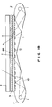
- JP-A 57-128383 A representative example of the H-arrangement- type backlight device for a transmission-type liquid crystal panel has been proposed by JP-A 57-128383 and Figure 21 is a schematic illustration thereof.
- a backlight device Bo includes a fluorescent lamp 1 as a light source and a reflector 2 disposed to surround the fluorescent lamp 1. Extending sidewards from the fluorescent lamp 1 is disposed a light-guide member 3 of a thick transparent plate of, e.g., acrylic resin. Behind the light-guide member 3, light-scattering layers 5 are disposed in a prescribed areal proportion. Light issued from the fluorescent lamp 1 and entering the light-guide member 3 is scattered by the scattering layers 5 and issued from the front face of the light-guide member 3 to illuminate a liquid crystal panel (not shown) at a uniform illuminance.
- a liquid crystal panel not shown
- the light-guide member 3 is composed of, e.g., an acrylic resin, and is therefore heavy, so that the backlight device becomes heavy and suffers from inferior conveyability.
- a liquid crystal panel size is enlarged so that the backlight is also enlarged. Accordingly, the light-guide member is thick and enlarged in area, so that the above-mentioned difficulty is promoted.
- JP-A 5-323318 a backlight device using no light-guide member has been proposed as in JP-A 5-323318.
- the backlight device has resulted in a poor planar illumination uniformity and is unsuitable for a large area display apparatus having a diagonal size of 38 cm (15 inches) or larger. Further, the backlight device is required have a backing reflector shaped in a parabolic curved surface and requires a substantial production cost.
- JP-A 5-281541 also discloses a backlight device capable of dispensing with a light-guide member, but the device also suffers from a poor planar illumination uniformity, which becomes noticeable in a large-area display apparatus having a diagonal display area size of 38 cm (15 inches) or larger.
- direct backing-type backlight devices generally require a large thickness behind display apparatus and are unsuitable for flat panel displays. Particularly, uniform illumination light cannot be attained for large area display apparatus unless a large number of light sources (fluorescent lamps) are used.
- direct backing-type backlight devices are liable to be complicated and expensive for a larger size and are believed to be unsuitable for flat panel-type display apparatus of an increasingly large display area.
- An object of the present invention is to provide a backlight device for display apparatus capable of issuing uniform illumination light without using a light-guide member occupying a substantial part of the total weight of such a backlight device, when used.
- Another object of the present invention is to provide a backlight device for display apparatus, which is light and excellent in portability.
- Another object of the present invention is to provide a backlight device for display apparatus capable of providing improved viewing angle characteristic and moire-freeness.
- Another object of the present invention is to provide a backlight device for display apparatus, capable of issuing uniform planar illumination light even for a large display area having a diagonal size of 38 cm (15 inches) or larger.
- a further object of the present invention is to provide a backlight device for display apparatus, capable of issuing uniform planar illumination light even at a relatively low accuracy of designing of a reflection layer and a disposition density thereof.
- a still further object of the present invention is to provide a backlight device for display apparatus capable of preventing an adverse effect of radiation heat from a light source to a display device.
- Sill another object of the present invention is to provide an inexpensive but reliable backlight device for display apparatus.
- a yet further object of the present invention is to provide a backlight device for display apparatus capable of issuing illumination light having uniform spectral characteristic at the illuminated surface.
- a backlight device comprising: reflection means for reflecting light, a transmission member disposed opposite to the reflection means so as to form a space from the reflection means, and a light source disposed to emit light into the space, so that light issued from the light source into the space is reflected by the reflection means and transmitted through the transmission member.
- the transmission member is provided with a reflection layer having a multitude of apertures, so that the light issued from the light source into the space is repetitively reflected by the reflection means and the reflection layer to be leaked outwards through the transmission member out of the apertures.
- the apertures are arranged to have an area per unit region of the transmission member, which area increases with an increase in distance from the light source.
- the reflection means is provided with a scattering layer for scattering and reflecting light on a face of the reflection means opposite to the reflection layer.
- the scattering layer is provided with a multitude of apertures arranged to have an area per unit region of the scattering layer, which area decreases with an increase in distance from the light source.
- the backlight device further includes a polarization beam splitter supported on the transmission member for selectively transmitting a p-polarization component and reflecting an s-polarization component, and a quarter wave plate disposed on the reflection means and opposite to the transmission member for causing conversion between the p-polarization component and the s-polarization component, whereby light emitted from the light source into the space is reflected between the polarization beam splitter layer and the reflection means so that the p-polarization component of the emitted light is selectively leaked outwards through the transmission member.
- a polarization beam splitter supported on the transmission member for selectively transmitting a p-polarization component and reflecting an s-polarization component
- a quarter wave plate disposed on the reflection means and opposite to the transmission member for causing conversion between the p-polarization component and the s-polarization component, whereby light emitted from the light source into the space is reflected between the polarization beam splitter layer and the reflection means so that the p-polarization component of
- a backlight device comprising:
- a display apparatus comprising:
- a transmission-type display device P is illuminated by a backlight device according to the invention including light sources 1, reflectors 2, a reflection means 10 and a transmission member 11 having a pattern of reflection layer.
- the light sources are disposed outside the display device P to form an edge-type or H(-arrangement)-type backlight device.
- the lamps are disposed with a spacing of at least M which is a lateral length of the display device P.
- the light source 1 may be any light source having a spectral distribution desired by the display device P. Specific examples thereof may include LEDs, halogen lamps, xenon lamps and white fluorescent lamps. Particularly, for a display device having three types of pixels of red (R), green (G) and blue (B), it is preferred to use a three-wavelength type white fluorescent lamp having a spectral characteristic of providing emission peaks in the regions of R, G and B, respectively.
- the reflectors 2 and reflecting means 10 may for example comprise a metal member having a reflecting inner surface or a light-absorbing or light-transmissive substrate coated with a reflective material forming an inner surface.
- the transmission member 11 may comprise a light-transmissive substrate surface-coated with pattern of reflection layer.
- the reflection layer pattern may preferably have apertures (portions free from the reflection layer) occupying an areal ratio (i.e., aperture ratio) which increases with an increase in distance in X-direction from a light source 1.
- aperture ratio is determined based on distances of 0 to M/2 from the light sources at the left and right ends.
- the reflection layer may have a pattern of a multitude of reflective portions of various shape, such as circles, ellipses, squares, rectangles, lozenges, parallelograms, trapezoids or stars.
- the apertures can assume various discrete shapes as descried above.
- the display device P may suitably comprise a liquid crystal device, examples of which may include: STN-type and DSTN-type liquid crystal devices using nematic liquid crystals; active matrix-type liquid crystal devices using thin-film transistors or MIM-elements; and ferroelectric liquid crystal devices and antiferroelectric liquid crystal devices using chiral smectic liquid crystals.
- a liquid crystal device examples of which may include: STN-type and DSTN-type liquid crystal devices using nematic liquid crystals; active matrix-type liquid crystal devices using thin-film transistors or MIM-elements; and ferroelectric liquid crystal devices and antiferroelectric liquid crystal devices using chiral smectic liquid crystals.
- the backlight device according to the present invention may preferably further comprise a prism sheet so as to have the direction of light issuance therefrom approach a planar normal.
- a prism sheet so as to have the direction of light issuance therefrom approach a planar normal.
- the reflecting means with a reflecting surface shaped so as to reduce the number of reflections thereat as will be described with reference to Figures 17 and 18, while a shaping step may be additionally required thereby.
- An embodiment of backlight device B 1 shown in Figure 2 is provided with a rear reflecting plate (reflection means) 10 composed of an aluminium
- the rear reflecting plate 10 has a mirror-finished surface so as to reflect light incident thereto.
- the reflecting plate is integrally formed with reflectors 2 having a concave surface composed also of an aluminum plate.
- a front transmission plate (transmission member) 11 of a thin transparent acrylic resin plate is disposed with a spacing from and in parallel with the reflecting plate 10, so that a space S is defined by the rear reflecting plate 10 and the front transmission plate 11.
- three wavelength-type fluorescent lamps 1 as linear light sources are disposed so that light emitted therefrom enters the space S directly or indirectly after reflection by the reflector 2.
- a reflection layer 12 of, e.g., vapour-deposited aluminium is disposed in a pattern of a mesh or various discrete shapes as described above to form a multitude of apertures 13, out of which light is allowed to leak out through the front transmission plate 11.
- a transmission-type liquid crystal panel (not shown) so that the liquid crystal panel is illuminated with the light issued from the backlight device Bi.
- the angle (denoted by “61” " in Figure 2) of light incident to the transmission plate 11 becomes smaller as the position leaves away from the fluorescent lamp 1 so that leakage quantity of the light becomes smaller in proportion to almost the angle 0, if the aperture ratio k is constant.
- the aperture ratio k(x) of the reflection layer 12 is set to be larger as the distance x increases, so that the leakage light quantities at various positions become substantially equal.
- the planar luminance distribution of the leakage light (illumination light) from the backlight device B 1 becomes uniform to provide an improved display quality to the liquid crystal panel.
- the light-guide member 3 ( Figure 21) required in the conventional device is omitted, so that the backlight device becomes lighter in weight by that much and provides an improved portability to even a large-area display apparatus.
- a front surface (opposite to a transmission plate 11 and a reflection layer 12) of a rear reflection plate 10 is provided with a scattering layer 20.
- the scattering layer 20 may be composed of a printed layer of a white pigment, such as barium sulphate, calcium carbonate or titanium oxide and, likewise the reflection layer 12, may be formed in a mesh pattern or a discrete dot pattern so as to provide a multitude of apertures 21.
- the aperture ratio k 1 (x) of the scattering layer 20 is set to be smaller as the distance from the fluorescent lamp increases, in contrast to the case of the reflection layer 2.
- the aperture ratio k(x) of the reflection layer 12 is set to be larger as the distance x from the fluorescent lamp 1 becomes larger, so that the leakage light quantities at various positions become almost equal.
- the leakage light (illumination light) from the backlight device B 2 is caused to have a uniform planar luminance distribution, thereby providing an improved display quality to the liquid crystal panel.
- the incident light angle 0 2 becomes smaller as the position is left away from the fluorescent lamp 1.
- the aperture ratio k 1 (x) of the scattering layer is set to be smaller so as to provide a larger occupation areal ratio (1-k, (x)) of the scattering layer 20 as the position is left away from the scattering layer 20.
- the scattered light is incident to the transmission plate 11 at a larger incident angle 0 3 to be more readily leaked out through the apertures 13 of the reflection layer 2.
- the backlight device can exhibit an improved performance for a larger area display apparatus.
- a front surface (upper surface) of a rear reflection plate 10 is provided with a X/4 plate 30 for effecting plarization conversion between an s-polarization component (light component having an electric field component perpendicular to the drawing sheet of Figure 4) and a p-polarization component (light component having an electric field component parallel to the drawing sheet of Figure 4), and a lower surface of a front transmission plate 11 is provided with a polarization beam splitter layer 31 of an optical multi-layer film, which allows the transmission of only the p-polarization component and reflects the s-polarization component.
- a liquid crystal panel (not shown) disposed above the plat 11 is designed to receive the p-polarized light as illumination light.
- the fluorescent lamp 1 When the fluorescent lamp 1 is turned on, emitted light is repetitively reflected between the rear reflecting plate 10 and the polarization beam splitter layer 31, and a p-polarization component of the light incident to the polarization beam splitter layer 31 is transmitted through the layer 31 and the front transmission plate 11 to be leaked outwards.
- the remaining s-polarization component is reflected by the polarization beam splitter layer 31 and then incident to and reflected by the rear reflection plate 10 where the s-polarization is converted to p-polarization because it passes twice the X/4 plate 30.
- the resultant p-polarization component is transmitted through the polarization beam splitter layer 31 and the front transmission plat 11 to be leaked outwards.
- the illumination efficiency of the backlight device can be remarkably improved.
- a front transmission plate 11 is composed of a transparent glass plate and the front surface of the front transmission plate 11 is provided with a reflection layer 12. Further, between a rear reflection plate 10 and a X/4 plate 30, a scattering layer 20 is disposed.
- the reflection layer 12 is formed in a dot pattern or a mesh pattern so as to have an aperture ratio k(x) increasing with an increase in distance from the fluorescent lamp 1 similarly as in the first embodiment, and the scattering layer 20 is formed in a dot or mesh pattern so as to provide a prescribed aperture ratio k 1 (x) similarly as in the second embodiment.
- an s-polarization component is reflected by a polarization beam splitter layer 31 and is then reflected by a rear reflection plate 10 where it is converted into a p-polarization component.
- a p-polarization component is transmitted through the polarization beam splitter 31, a portion thereof is leaked out of the apertures 13 to illuminate a liquid crystal panel (not shown) disposed above, and the remaining portion thereof is reflected by the reflection layer 12 to enter the space S again.
- the portion of the p-polarization component reflected by the reflection layer 12 is converted into an s-polarization component when it is reflected by the rear reflection plate 10.
- the s-polarization component is again reflected by the polarization beam splitter layer 31 and the rear reflection plate 10, where it is again converted into a p-polarization component allowed to be leaked outwards similarly as the above for illuminating the liquid crystal panel.
- the aperture ratio k(x) of the reflection layer 12 is set to be larger a the distance x from the fluorescent lamp 1 increases, the light leakage quantities at various positions become almost equal, so that the leakage light (illumination light) from the backlight device B 3 is caused to have a uniform planar luminance distribution, thereby providing an improved display quality to the liquid crystal panel.
- the illumination light angle characteristic is uniformized regardless of the distance from the fluorescent lamp 1 and the leakage light quantities at various positions are made almost equal, so that the planar luminance distribution is uniformized also in this respect to provide an improved display quality of the liquid crystal panel.
- a the aperture ratio k 1 (x) of the scattering layer 20 is set to be smaller as the distance x from the fluorescent lamp 1 increases, a fraction of light incident at a smaller incident angle 0 2 is more easily scattered, so that the leakage light quantities from various positions of the backlight device are equalized also in this respect, leading to a uniform planar luminance distribution of the backlight device B 4 and an improved display quality of the liquid crystal panel.
- the utilization efficiency of the backlight illumination light can be remarkably improved.
- the fluorescent lamp 1 is indicated but it is possible to dispose an additional fluorescent lamp at a position opposite to the fluorescent lamp 1 so as to dispose the reflection plate 10 and the transmission plate 11 between the resultant pair of fluorescent lamps similarly as shown in Figure 1.
- the number of fluorescent lamps is not limited to 2 but may be 4 so as to surround the space S. By this arrangement, it is possible to provide a backlight device with an increased luminous intensity.
- the reflection layer 12 is disposed on the upper surface of the front transmission plate but this is not limitative.
- a reflection layer may also be disposed on a lower surface (confronting with the X/4 plate 30) of the front transmission plate 11.
- the apertures in the reflection layer are arranged to have an aperture ratio which increases with an increase in distance from a light source, the light leakage quantities at respective positions are substantially equalized to provide a uniform planar luminance distribution of leakage light (illumination light).
- the reflection means is provided with a scattering layer for scattering and reflecting light incident thereto, the angle characteristic of issued light can be uniformized to equalize the leakage light quantities, thereby providing a uniform planar luminance distribution of illumination light.
- the scattering layer is provided with a multitude of apertures providing an aperture ratio which decreases with an increase in distance from the light source, a light fraction having a smaller incident angle is subjected to a promoted scattering to increase the light leakage through the apertures of the reflection layer thereat. This also promotes the equalization of leakage lights from the backlight device leading to a uniform planar luminance distribution of illumination light.
- a backlight device B includes the fluorescent lamps 1 as linear light sources, which are disposed opposite to each other with a spacing therebetween and so as to be covered with reflectors 2 as shown in Figure 9.
- a rear reflecting plate (first reflection means) 10 is disposed integrally with the reflectors 2, which are integrally composed of an aluminum plate so as to reflect emitted light from the fluorescent lamps 1.
- a front transmission plate 11 is disposed in parallel with the rear reflection plate 10.
- the front transmission plate 11 may be composed of a relatively thin transparent acrylic resin plate.
- a reflection layer (second reflection means) 12 is disposed opposite to the rear reflecting plate 10 with a space S therebetween.
- the reflection layer 12 may be formed of, e.g., a vapor-deposited aluminum film in a mesh or dot pattern so as to provide apertures designed to have a prescribed aperture ratio distribution.
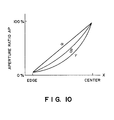
- the aperture ratio of the apertures is designed to increase with an increase in distance from the nearest fluorescent lamp 1. More specifically, the aperture ratio Ap is designed to satisfy a relationship represented by a curve in Figure 10 which is intermediate between a linear relationship a and a parabolic relationship y in Figure 10, with respect to the distance x from the lamp 1.
- the fluorescent lamps 1 are disposed to emit light toward a prescribed space S formed between the rear reflection plate 10 and the reflection layer 12.
- the space S functions as a light-guide space for directing the emitted light from the fluorescent lamps 1 upwards in the drawing.
- the reflection layer 12 is formed to provide an aperture ratio as described above, a portion of light L1 ( Figure 8) is transmitted through the reflection layer 12 and the remaining portion of light L2 is reflected toward the rear reflection plate 10.
- two prism sheets (prism means) 16 and 17 provided with a multitude of prism elements each having an apex angle of 90 degrees.
- the prism elements are disposed so that their ridges providing apex angles extend in parallel with the longitudinal direction of the fluorescent lamp 1 and the apex angles are disposed on a reverse side (upwards) with respect to the rear reflection plate 10 of the transmission plate 11.
- a liquid crystal panel (not shown) to be illuminated is disposed above the prism sheets 16 and 17, a liquid crystal panel (not shown) to be illuminated is disposed.
- the emitted light is repetitively reflected between the rear reflecting plate 10 and the reflection layer 12 to proceed in the space S. Then, a portion of light L1 is transmitted through the apertures 13 having a prescribed aperture ratio in the reflection layer 12 and is further transmitted through the prism sheets 16 and 17 to be issued in a direction deflected toward a normal to the prism sheets 16 and 17.
- the leakage light quantities at various positions of the reflection layer 12 are adjusted by the aperture ratio distribution therein to provide illumination light having a uniform planar luminance distribution.
- the prescribed space S formed between the rear reflection plate 10 and the reflection layer 12 is utilized as a light-guide space to omit a thick acrylic resin plate conventionally used, the backlight device is decreased in weight by that much.
- the luminance distribution of light from a backlight device assumes peaks at emission angles (viewing angles) of ⁇ 60 °C as shown in Figure 11A, thus showing an insufficient light-condensing performance and failing to provide an improved viewing angle characteristic.
- the light-condensing performance is improved to provide an improved viewing angle characteristic as shown in Figure 11 B.
- the aperture ratio distribution in this embodiment is set as represented by a curve in Figure 10, and a uniform luminance distribution as represented by a curve in Figure 12 can be attained.
- a backlight device B is provided with one prism sheet (prism means) 21 having a multitude of prism elements each having an apex angle of 60 degrees thereon.
- the prism elements are disposed so that their ridges providing the apex angles extended in parallel with the longitudinal direction of the fluorescent lamp 1 and the apex angles are directed upwards (toward a liquid crystal panel (not shown) and against the rear reflection plate 10).
- the reflection layer 12 is similarly set to have an aperture ratio distribution represented by a curve in Figure 10, and the other arrangements are also similar to those adopted in the previous sixth embodiment.
- the prism sheet 21 having an apex angle of 60 degrees is used, so that light L1 transmitted through the transmission plate 11 is refractively deflected in a direction deviated toward a normal to the prism sheet 21, so that the viewing angle characteristic of the backlight device is improved similarly as in the previous sixth embodiment.
- the cost and the weight of the backlight device are reduced.
- the space S formed between the rear reflection plate 10 and the reflection layer 12 is utilized as a light-guide space to omit a thick acrylic resin plate conventionally used as a light-guide member, so that the weight is reduced by that much.
- the aperture ratio distribution in the reflection layer 12 in this embodiment is set to satisfy the curve in Figure 10, the resultant planar luminance distribution becomes uniform as represented by the curve in Figure 12.
- a backlight device B is provided with one prism sheet (prism means) 31 having a multitude of prism elements each having an apex angle of 60 degrees thereon as shown in Figure 14.
- the prism elements are disposed so that their ridges providing the apex angles extended in parallel with the longitudinal direction of the fluorescent lamp 1 and the apex angles are directed downwards (toward the front transmission plate 11 and the rear reflection plate 10).
- the reflection layer 12 is similarly set to have an aperture ratio distribution represented by a curve in Figure 10, and the other arrangements are also similar to those adopted in the previous sixth embodiment.
- the prism sheet 21 having an apex angle of 60 degrees directed downwards is used, so that light L1 transmitted through the transmission plate 11 is deflected and emitted in a direction close to a normal to the prism sheet 21, so that the viewing angle characteristic of the backlight device is improved as shown in Figure 15.
- the space S formed between the rear reflection plate 10 and the reflection layer 12 is utilized as a light-guide space to omit a thick acrylic resin plate conventionally used as a light-guide member, so that the weight is reduced by that much.
- the aperture ratio distribution in the reflection layer 12 in this embodiment is set to satisfy the curve in Figure 10, the resultant planar luminance distribution becomes uniform as represented by the curve in Figure 12.
- the upper surface of the front transmission plate 11 with a diffusion treatment, whereby a uniform luminance of illumination light can be attained regardless of the aperture pattern of the reflection layer 12.
- a diffusion plate or sheet on the front transmission plate 11 or the upper prism sheet 17.
- a diffusion means 61 such as a diffusion plate or sheet, between the two prism sheets 16 and 17 as shown in Figure 16.
- a pair of fluorescent lamps 1 are disposed opposite to each other but this is of course not limitative.
- a fluorescent lamp 1 on one side of the light-guide space S and dispose a reflection plate on the other side opposite to the fluorescent lamp 1.
- the backlight device can be reduced in size and weight.
- two fluorescent lamps 1 are used, but four fluorescent lamps can be used so as to surround the light-guide space S.
- the prism ridges on one prism sheet extend longitudinally (in the thickness of the drawing sheet as shown) and the prism ridges on the other prism sheet extend laterally, i.e., the prism ridges on the prism sheets cross each other at right angles.
- the aperture ratios in the reflection layer 12 are caused to have a two-dimensional distribution.
- the aperture ratio of the reflection layer 12 is set to have a distribution represented by the curve in Figure 10, but this is not limitative.
- the aperture ratio distribution can be linear as represented by a curve a in Figure 10 or parabolic as represented by a curve y in Figure 10. In either case, a substantially uniform planar luminance distribution can be attained as shown by curves a and y in Figure 12.
- the prism sheets having a prism apex angle of 60 degrees are used, but the apex angle can be any angle below 90 degrees, preferably in the range of 50 - 70 degrees.
- light emitted from a linear light source is caused to enter a space formed between first and second reflection means where no light-guide member like that of a thick acrylic resin plate is disposed. Accordingly, the backlight device can be reduced in weight by omission of such a light-guide member.
- the light transmitted through (the apertures of) the second reflection means is deflected into a direction which is closer to a normal to the prism means, whereby the viewing angle characteristic of the backlight device can be improved.
- the viewing angle characteristic is further improved in case where plural sheets of prism means are used.
- an improved viewing angle characteristic can be attained if the apex angle is made smaller than 90 degrees, preferably in the range of 50 - 70 degrees.
- the prism means is disposed so that their apexes are directed toward the first reflection means (i.e., against the illumination object), the viewing angle characteristic is further improved.
- the second reflection means is provided with apertures designed to have a distribution of aperture ratio which increases with an increase in distance from a linear light source, e.g., in a relationship of a linear, a parabolic or an intermediate therebetween, the planar luminance distribution of the backlight device can be uniformized.
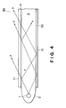
- FIG 17 is a sectional view of a ninth embodiment of the backlight device according to the present invention.
- a backlight device includes a pair of linear light sources 1, reflectors 2, a rear reflection plate 10 and a front transmission plate 11 of a relatively thin acrylic resin plate.
- the reflectors 2 and the rear reflection plate 10 are composed integrally of an aluminum plate mirror-finished by a vapor-deposited Ag film.
- the rear reflection plate 10 is shaped to have a projecting or rising center (ridge) as shown.
- a space S defined between the rear reflection plate 10 and the front transmission plate 11 is caused to have a narrower spacing than at the lateral parts in the neighborhood of the light sources 1, and the space S functions as a light-guide space for guiding emitted light from the light sources 1 laterally.
- An upper side 88 of the front transmission plate 11 functions as an illumination surface, above which a liquid crystal panel P is disposed.
- the lower surface of the front transmission plate 11 is provided with a reflection layer 12 of vapor-deposited AI in a mesh or dot pattern having a prescribed aperture ratio, which may be referred to as a so-called lighting curtain.
- the aperture ratio is designed to increase with an increase in distance from the nearest light source 1.
- An entire structure of the backlight device is laterally almost symmetrical with two light sources 1 on lateral sides of the light-guide space S as shown in Figure 17.
- emitted light from the light sources 1 is repetitively reflected by the rear reflection plate 10 and the reflection layer 12 to proceed toward the center of the light- guides space S.
- the central portion of the rear reflection plate 10 is projected upwards, so that a portion of the emitted light from the light sources 1 is allowed to reach the center of the light-guide space S by a single reflection at the rear reflection plate 10.
- the light is allowed to leak upwards through the apertures in the reflection layer 12, and the resultant leakage light functions as illumination light.
- the emitted light reaches the center of the light-guide space S in a smaller number of reflections to be utilized as illumination light, so that the illumination light is less affected by the spectral reflection characteristics of the rear reflection plate 10 and the reflection layer 12 to alleviate color irregularity or deviation between the central part and the peripheral part of the backlight device.
- the illumination light quantities at respective positions are adjusted by an aperture ratio distribution in the reflection layer 11, which may preferably be set to have an increasing aperture ratio with an increase in distance from the edges of the light-guide space S on the light source sides toward the center of the space S. Further, it is also possible to dispose a diffusion plate or sheet separately above the front transmission plate 11 so as to observe the pattern of the reflection layer 12 liable to appear on the illumination surface.
- the backlight device of this embodiment has a laterally symmetrical arrangement as shown in Figure 17 and two light sources are disposed on laterally opposite sides of the light-guide space. It is, however, possible to dispose a light source only on a left side of the light-guide space by disposing a reflection means on the right side so as to be opposite to the reflector on the left side. This arrangement may rather be more suitable for a small-size backlight device. On the other hand, it is also possible to dispose light sources on peripheral four sides of the light-guide space by developing the above-described arrangement laterally (as shown) and also longitudinally (in the direction of thickness of the drawing sheet). In this case, it is preferred that the aperture ratios in the reflection layer 12 are also caused to have a two-dimensional distribution. Further, in place of the front transmission plate 11 of an acrylic resin plate having the reflection layer 12, it is also possible to use a PET sheet having an AI reflection layer, i.e., a so-called lighting curtain, so as to attain a similar function.
- an AI reflection layer
- FIG 18 is a sectional view of a tenth embodiment of the backlight device according to the present invention.
- a backlight device includes a pair of linear light sources 1, reflectors 2, a rear reflection plate 10 and a front transmission plate 11 of a relatively thin acrylic resin plate.
- the reflectors 2 and the rear reflection plate 10 are composed integrally of an aluminum plate mirror-finished by a vapor-deposited Ag film.
- the rear reflection plate 10 is shaped to have a projecting or rising center (ridge) as shown.
- a space S defined between the rear reflection plate 10 and the front transmission plate 11 is caused to have a narrower spacing than at the lateral parts in the neighborhood of the light sources 1, and the space S functions as a light-guide space for guiding emitted light from the light sources 1 laterally.
- An upper side 88 of the front transmission plate 11 functions as an illumination surface, above which a prism sheet 31 is disposed.
- the prism sheet 31 is provided with a multitude of prism elements forming ridges extending parallel with the longitudinal direction of the light sources 1 and having apexes directed downwards (toward the front transmission plate 11. Above the prism sheet 31, a liquid crystal panel P is disposed as an object to be illuminated.
- the lower surface of the front transmission plate 11 is provided with a reflection layer 12 of vapor-deposited AI in a mesh or dot pattern having a prescribed aperture ratio.
- the aperture ratio is designed to increase with an increase in distance from the nearest light source 1.
- An entire structure of the backlight device is laterally almost symmetrical with two light sources 1 on lateral sides of the light-guide space S as shown in Figure 18.
- emitted light from the light sources 1 is repetitively reflected by the rear reflection plate 10 and the reflection layer 12 to proceed toward the center of the light- guides space S.
- the central portion of the rear reflection plate 10 is projected upwards, so that a portion of the emitted light from the light sources 1 is allowed to reach the center of the light-guide space S by a single reflection at the rear reflection plate 10.
- the light In the process of propagation through the light-guide space S, the light is allowed to leak upwards through the apertures in the reflection layer 12, and the resultant leakage light functions as illumination light, wherein the illumination light quantities at respective positions are adjusted by an aperture ratio distribution in the reflection layer 12, which may preferably be set to have an increasing aperture ratio with an increase in distance from the edges of the light-guide space S on the light source sides toward the center of the space S.
- the portion of light emitted through the front transmission plate 11 mostly have a large emission angle of around 60 degrees (with respect to a normal to the front transmission plate 11 but may be totally reflected at a prism surface on the prism sheet 31 to be deflected toward a frontal direction of the illumination surface.
- the prism apex angle may preferably be around 60 degrees. Further, it is also possible to dispose a diffusion plate or sheet separately between the front transmission plate 11 and the prism sheet 31 or above the prism sheet 31 so as to observe the pattern of the reflection layer 12 liable to appear on the illumination surface.
- the emitted light reaches the center of the light-guide space S in a smaller number of reflections to be utilized as illumination light, so that the illumination light is less affected by the spectral reflection characteristics of the rear reflection plate 10 and the reflection layer 12 to alleviate color irregularity or deviation between the central part and the peripheral part of the backlight device.
- a prism sheet 31 having the above-described function is added, the luminance in the frontal direction is remarkably increased.
- the backlight device of this embodiment has a laterally symmetrical arrangement as shown in Figure 18 and two light sources are disposed on laterally opposite sides of the light-guide space. It is, however, possible to dispose a light source and a light-transmissive sheet member only on a left side of the light-guide space by disposing a reflection means on the right side so as to be opposite to the reflector on the left side. This arrangement may rather be more suitable for a small-size backlight device. ON the other hand, it is also possible to dispose light sources on peripheral four sides of the light-guide space by developing the above-described arrangement laterally (as shown) and also longitudinally (in the direction of thickness of the drawing sheet).
- the prism ridges on one prism sheet extend longitudinally (in the thickness of the drawing sheet as shown) and the prism ridges on the other prism sheet extend laterally, i.e., the prism ridges on the prism sheets cross each other at right angles.
- the aperture ratios in the reflection layer 12 are caused to have a two-dimensional distribution.
- a PET sheet having an AI reflection layer i.e., a so-called lighting curtain, so as to attain a similar function.
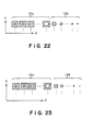
- Figures 22 and 23 are respectively a plan view showing a preferred reflection layer pattern (aperture pattern) used in the present invention.
- the X-Y coordinates in these figures correspond to that shown in Figure 1, and a larger x represents a larger distance from a light source 1.
- the reflection layer pattern is depicted only one-dimensionally in the X-direction but actually the pattern may be repeated in the Y direction.
- the reflective layer patterns shown in Figures 22 and 23 respectively include a sub-pattern 12a and a sub-pattern 12b.
- the sub-pattern 12a comprises a continuous masking layer (shown with a hatching, illustrated as discrete square patterns for convenience of illustration but may actually constitute a continuous layer) and discrete apertures having an aperture ratio increasing with an increase in X-coordinate.
- the sub-pattern 12a is suitable for providing aperture ratios in a range of, e.g., 0 - 50 %.
- the sub-pattern 12b is a negative (or complementary) pattern with respect to the sub-pattern 12a, i.e., comprises discrete masking layers and a continuous aperture (or opening) area surrounding the masking layers.
- the sub-pattern 12b is suitable for providing aperture ratios in the range of, e.g., 50 - 100 %. It is clear that the boundary aperture ratio for selection of the sub-patterns 12a and 12b is not necessarily 50 %.
- the patterns of Figures 22 and 23 may be formed laterally symmetrically with a line (extending longitudinally) of aperture ratio of 100 % at the center.
- Some sample backlight devices for a display panel having a diagonal size of 15 inches were prepared and evaluated in the following manner.
- sample devices a - d were prepared to have structures corresponding to Figures 2, 13, 8 and 14, respectively, and provided with white fluorescent lamps 1 each having a broad spectral characteristic over the regions of R, G and B.
- Sample devices were prepared similarly to have structures corresponding to Figures 2, 13, 8 and 14, respectively, but provided with three wavelength-type white fluorescent lamps 1 each having a spectral characteristic showing steep peaks in the three wavelength regions of R, G and B, respectively, instead of the above white fluorescent lamps having a broad spectral characteristic.
- the luminance was measured at a large number of points on the light emission surface of the device so as to evaluate the uniformity of luminance of illumination light. More specifically, the difference between the maximum luminance and the average luminance was obtained, and the reciprocal of the difference was used for evaluation.
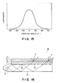
- the luminance change of illumination light was evaluated at various viewing positions. More specifically, a luminance-viewing angle characteristic curve a shown in Figures 11 and 15 was obtained to measure a half-width value (degree). The reciprocal of the half-width value was used for evaluation.
- a chiral smectic liquid crystal display panel and a twisted nematic liquid crystal active matrix-type display panel were respectively illuminated with a sample device to evaluate whether the color reproducibility was uniform within the display panel. More specifically, a triangle having three corners representing R, G and B was depicted on a CIE color coordinate system and the area of the triangle was measured. The area representing a measure of color reproducing ability was used for evaluation.
- sample devices were judged as "A” if all the ten panelists judged to be excellent, "C” if no one judged to be excellent, and "B” for an intermediate judgment.
- the data transmission apparatus 400 includes a liquid crystal panel (display device) P so as to display various data or information by the panel P.
- a liquid crystal panel includes a pair of oppositely disposed substrates, and a liquid crystal disposed between the substrates.
- the pair of substrates are provided with scanning electrodes and data electrodes so as to form an electrode matrix.
- the liquid crystal panel P is connected to a scanning signal application circuit 402 and a data signal transmission circuit 403, which are in turn further connected to a scanning signal control circuit 404 and a data signal control circuit 406, a drive control circuit 405 and a graphic controller 407, sequentially.
- data and scanning scheme signals are supplied from the graphic controller 407 via the drive control circuit 405 to the scanning signal control circuit 404 and the data signal control circuit 406, where the data are converted into address data and display data and the other scanning scheme signals are sent as they are to the scanning signal application circuit 402 and the data signal application circuit 403.
- the scanning signal application circuit 402 applies a scanning signal having a waveform determined by the scanning scheme signals to a scanning electrode determined by the address data
- the data signal application circuit 403 applies data signals having waveforms determined by both display contents of white or black based on the display data and the scanning scheme signals.
- a liquid crystal display apparatus 50 is provided with a backlight device according to any one of the above-descried embodiments.
- the backlight device 10 is connected to a backlight lighting circuit (backlight drive means) 51 so as to drive the backlight device 10.
- a liquid crystal panel P which comprises a pair of oppositely disposed glass substrates provided with scanning electrodes and data electrodes, and a ferroelectric liquid crystal disposed between the glass substrates.
- the scanning electrodes and data electrodes are connected to X-drivers 52 and a Y-driver 53, respectively, which in turn are corrected to a panel drive controller (liquid crystal device drive means) 55.
- the panel drive controller 55 and the backlight lighting circuit 51 are connected to a power supply unit 56 so as to supply powers. Further, panel drive controller is connected to a host computer (not shown) to be supplied with display signals. On the other hand, based on the display signals, the panel drive controller 55 supplies signals to the liquid crystal panel P via the drivers 52 and 53. Further, the panel drive controller 55 supplies ON/OFF signals and lighting control signals to the backlight lighting circuit 51, which drives the backlight device 10 based on such signals.
Abstract
Description
- The present invention relates to a backlight device for display apparatus, such as those for computers, word processors, television receivers and navigation systems, and view finders for video cameras.
- Backlight devices or display apparatus may be classified into the direct backing-type and the edge (or H-arrangement)-type. Examples of the former type have been disclosed in Japanese Laid-Open Patent Appln. (JP-A) 2-39118 and JP-A 6-18873, and examples of the latter type have been disclosed in JP-A 63-13202, JP-A 4-71105, JP-A 5-281541 and JP-A 5-323318. A representative example of the H-arrangement- type backlight device for a transmission-type liquid crystal panel has been proposed by JP-A 57-128383 and Figure 21 is a schematic illustration thereof.
- Referring to Figure 21, a backlight device Bo includes a
fluorescent lamp 1 as a light source and areflector 2 disposed to surround thefluorescent lamp 1. Extending sidewards from thefluorescent lamp 1 is disposed a light-guide member 3 of a thick transparent plate of, e.g., acrylic resin. Behind the light-guide member 3, light-scatteringlayers 5 are disposed in a prescribed areal proportion. Light issued from thefluorescent lamp 1 and entering the light-guide member 3 is scattered by thescattering layers 5 and issued from the front face of the light-guide member 3 to illuminate a liquid crystal panel (not shown) at a uniform illuminance. - In the above-mentioned backlight device, the light-
guide member 3 is composed of, e.g., an acrylic resin, and is therefore heavy, so that the backlight device becomes heavy and suffers from inferior conveyability. Particularly, in recent years, a liquid crystal panel size is enlarged so that the backlight is also enlarged. Accordingly, the light-guide member is thick and enlarged in area, so that the above-mentioned difficulty is promoted. - For the above reason, a backlight device using no light-guide member has been proposed as in JP-A 5-323318. The backlight device has resulted in a poor planar illumination uniformity and is unsuitable for a large area display apparatus having a diagonal size of 38 cm (15 inches) or larger. Further, the backlight device is required have a backing reflector shaped in a parabolic curved surface and requires a substantial production cost.
- JP-A 5-281541 also discloses a backlight device capable of dispensing with a light-guide member, but the device also suffers from a poor planar illumination uniformity, which becomes noticeable in a large-area display apparatus having a diagonal display area size of 38 cm (15 inches) or larger.
- On the other hand, direct backing-type backlight devices generally require a large thickness behind display apparatus and are unsuitable for flat panel displays. Particularly, uniform illumination light cannot be attained for large area display apparatus unless a large number of light sources (fluorescent lamps) are used. Anyway, direct backing-type backlight devices are liable to be complicated and expensive for a larger size and are believed to be unsuitable for flat panel-type display apparatus of an increasingly large display area.
- Accordingly, it has been desired to develop an improved edge-type or H-(arrangement-)type backlight device, instead of a direct backing-type device, through elimination of various difficulties of the edge-type backlight device.
- An object of the present invention is to provide a backlight device for display apparatus capable of issuing uniform illumination light without using a light-guide member occupying a substantial part of the total weight of such a backlight device, when used.
- Another object of the present invention is to provide a backlight device for display apparatus, which is light and excellent in portability.
- Another object of the present invention is to provide a backlight device for display apparatus capable of providing improved viewing angle characteristic and moire-freeness.
- Another object of the present invention is to provide a backlight device for display apparatus, capable of issuing uniform planar illumination light even for a large display area having a diagonal size of 38 cm (15 inches) or larger.
- A further object of the present invention is to provide a backlight device for display apparatus, capable of issuing uniform planar illumination light even at a relatively low accuracy of designing of a reflection layer and a disposition density thereof.
- A still further object of the present invention is to provide a backlight device for display apparatus capable of preventing an adverse effect of radiation heat from a light source to a display device.
- Sill another object of the present invention is to provide an inexpensive but reliable backlight device for display apparatus.
- A yet further object of the present invention is to provide a backlight device for display apparatus capable of issuing illumination light having uniform spectral characteristic at the illuminated surface.
- According to the present invention accomplished in view of the above-mentioned circumstances, there is provided a backlight device, comprising: reflection means for reflecting light, a transmission member disposed opposite to the reflection means so as to form a space from the reflection means, and a light source disposed to emit light into the space, so that light issued from the light source into the space is reflected by the reflection means and transmitted through the transmission member. In this instance, it is preferred that the transmission member is provided with a reflection layer having a multitude of apertures, so that the light issued from the light source into the space is repetitively reflected by the reflection means and the reflection layer to be leaked outwards through the transmission member out of the apertures. It is also preferred that the apertures are arranged to have an area per unit region of the transmission member, which area increases with an increase in distance from the light source. It is further preferred that the reflection means is provided with a scattering layer for scattering and reflecting light on a face of the reflection means opposite to the reflection layer. It is also preferred that the scattering layer is provided with a multitude of apertures arranged to have an area per unit region of the scattering layer, which area decreases with an increase in distance from the light source. It is further preferred that the backlight device further includes a polarization beam splitter supported on the transmission member for selectively transmitting a p-polarization component and reflecting an s-polarization component, and a quarter wave plate disposed on the reflection means and opposite to the transmission member for causing conversion between the p-polarization component and the s-polarization component, whereby light emitted from the light source into the space is reflected between the polarization beam splitter layer and the reflection means so that the p-polarization component of the emitted light is selectively leaked outwards through the transmission member.
- According to another aspect of the present invention, there is provided a backlight device, comprising:
- a first reflection means for reflecting light,
- a second reflection means disposed opposite to the first reflection means so as to form a space therebetween and provided with apertures having a prescribed aperture ratio distribution,
- at least one linear light source disposed to emit light into the space, and
- at least one sheet of prism means having a multitude of prism ridges extending parallel with the linear light source,
- so that light emitted from the linear light source is repetitively reflected between the first and second reflection means, and a portion of the light is transmitted through the second reflection means and the prism means to be emitted in a direction deflected toward a normal to the prism means.
- According to the present invention, there is further provided a display apparatus, comprising:
- a backlight device as described above,
- a backlight drive means for driving the backlight device,
- a display device, particularly a liquid crystal display device, illuminated by the backlight device, and
- a drive means for driving the display device.
- These and other objects, features and advantages of the present invention will become more apparent upon a consideration of the following description of the preferred embodiments of the present invention taken in conjunction with the accompanying drawings, wherein like parts are denoted by like reference numerals.
-
- Figure 1 is a schematic exploded illustration of a backlight device according to the present invention.
- Figures 2 - 5 are sectional views for illustrating first to fourth embodiments, respectively, of backlight device according to the invention.
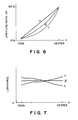
- Figures 6 and 7 are graphs showing an aperture ratio distribution in a reflection layer and a luminance distribution, respectively, of a fifth embodiment of the backlight device according to the invention.
- Figure 8 is a sectional view for illustrating a sixth embodiment of the backlight device according to the invention.
- Figure 9 is a schematic exploded illustration of the sixth embodiment of the backlight device according to the invention.
- Figure 10 is a graph showing an aperture ratio distribution of a prism sheet in the sixth embodiment of the backlight device according to the invention.
- Figures 11 A and 11B are graphs showing viewing angle-dependence of luminance in cases of using one prism sheet and two prism sheets,
- Figure 12 is a graph showing a planar luminance distribution in the sixth embodiment of the backlight device.
- Figures 13 and 14 are sectional views for illustrating 7th and 8th embodiments of the backlight device according to the invention.
- Figure 15 is a graph showing a viewing angle-dependence of luminance regarding the effect of the 8th embodiment.
- Figure 16 is a sectional view for illustrating a position of diffusion means.
- Figures 17 and 18 are sectional views for illustrating 9th and 10th embodiments of the backlight device according to the invention.
- Figures 19 and 20 are respectively a block diagram of a display apparatus using a backlight device according to the invention.
- Figure 21 is a schematic sectional view of a conventional backlight device.
- Figures 22 and 23 are respectively a plan view showing a preferred reflection layer pattern.
- A preferred embodiment of the backlight device according to the present invention will be described with reference to Figure 1, an exploded perspective view thereof.
- Referring to Figure 1, a transmission-type display device P is illuminated by a backlight device according to the invention including
light sources 1,reflectors 2, a reflection means 10 and atransmission member 11 having a pattern of reflection layer. - The light sources are disposed outside the display device P to form an edge-type or H(-arrangement)-type backlight device. In other words, when the
light light sources 1 are constituted by a pair of lamps, the lamps are disposed with a spacing of at least M which is a lateral length of the display device P. - The
light source 1 may be any light source having a spectral distribution desired by the display device P. Specific examples thereof may include LEDs, halogen lamps, xenon lamps and white fluorescent lamps. Particularly, for a display device having three types of pixels of red (R), green (G) and blue (B), it is preferred to use a three-wavelength type white fluorescent lamp having a spectral characteristic of providing emission peaks in the regions of R, G and B, respectively. - The
reflectors 2 and reflectingmeans 10 may for example comprise a metal member having a reflecting inner surface or a light-absorbing or light-transmissive substrate coated with a reflective material forming an inner surface. - The
transmission member 11 may comprise a light-transmissive substrate surface-coated with pattern of reflection layer. The reflection layer pattern may preferably have apertures (portions free from the reflection layer) occupying an areal ratio (i.e., aperture ratio) which increases with an increase in distance in X-direction from alight source 1. In the embodiment of Figure 1 having twolight sources 1 at both ends in the X-direction, the aperture ratio is determined based on distances of 0 to M/2 from the light sources at the left and right ends. - The reflection layer may have a pattern of a multitude of reflective portions of various shape, such as circles, ellipses, squares, rectangles, lozenges, parallelograms, trapezoids or stars. Alternatively, as a negative or complementary pattern to the above-mentioned reflective portions, the apertures can assume various discrete shapes as descried above.
- The display device P may suitably comprise a liquid crystal device, examples of which may include: STN-type and DSTN-type liquid crystal devices using nematic liquid crystals; active matrix-type liquid crystal devices using thin-film transistors or MIM-elements; and ferroelectric liquid crystal devices and antiferroelectric liquid crystal devices using chiral smectic liquid crystals.
- In the case of a liquid crystal device using a chiral smectic liquid crystal, there has been reported a liquid crystal molecular movement resulting in a change in liquid crystal layer thickness and causing a yellow-tinging or a display area (U.S. Patent No. 5,381,256). Accordingly, if the spectral characteristic of illumination light is changed to have a yellowish tint, the yellow tinging is liable to be enhanced. For this reason, it is preferred to use a backlight device of the present invention free from spectral characteristic change in combination with a chiral smectic liquid crystal device for obviating the above difficulty.
- In addition to the structure shown in Figure 1, the backlight device according to the present invention may preferably further comprise a prism sheet so as to have the direction of light issuance therefrom approach a planar normal. In this instance, it is particularly preferred to use a plurality of prism sheets so that their convex surfaces are directed toward a display device side as will be described with reference to Figure 8 or use a prism sheet disposed to have its convex surface directed toward a reflecting means 10 as will be described with reference to Figure 14. Further, it is also possible to provide the reflecting means with a reflecting surface shaped so as to reduce the number of reflections thereat as will be described with reference to Figures 17 and 18, while a shaping step may be additionally required thereby.
- An embodiment of backlight device B1 shown in Figure 2 is provided with a rear reflecting plate (reflection means) 10 composed of an aluminium The
rear reflecting plate 10 has a mirror-finished surface so as to reflect light incident thereto. The reflecting plate is integrally formed withreflectors 2 having a concave surface composed also of an aluminum plate. In front of therear reflecting plate 10, a front transmission plate (transmission member) 11 of a thin transparent acrylic resin plate is disposed with a spacing from and in parallel with the reflectingplate 10, so that a space S is defined by therear reflecting plate 10 and thefront transmission plate 11. At the lateral ends (e.g., the parts surrounded by the reflectors 2), three wavelength-type fluorescent lamps 1 as linear light sources are disposed so that light emitted therefrom enters the space S directly or indirectly after reflection by thereflector 2. - On the other hand, on the lower surface (i.e., opposite to the rear reflection plate 10) of the
front transmission plate 11, areflection layer 12 of, e.g., vapour-deposited aluminium is disposed in a pattern of a mesh or various discrete shapes as described above to form a multitude ofapertures 13, out of which light is allowed to leak out through thefront transmission plate 11. - In this embodiment, the
apertures 13 are arranged to have an aperture ratio k(x), i.e., a ratio of an area occupied by theapertures 13 per unit region of thefront transmission plate 11 at a position disposed at a distance x from the nearestfluorescent lamp 1, which aperture ratio increases with an increase in the distance x, e.g., in a relationship of 1-k(x) = a/x, wherein a is a proportional constant. - Above the
front transmission plate 11 is disposed a transmission-type liquid crystal panel (not shown) so that the liquid crystal panel is illuminated with the light issued from the backlight device Bi. - When the
fluorescent lamp 1 is turned on, light emitted from the fluorescent lamp enters the space S directly or after being reflected by thereflector 2. The light having entered the space is repetitively reflected by the reflectinglayer 12 and therear reflection plate 10 disposed opposite to each other, so that the space S functions as a light-guide space. Then, a portion of the light is leaked out through theapertures 13 of thereflection layer 12 and thetransparent plate 11 to illuminate a liquid crystal panel (not shown) disposed above theplate 11. - The angle (denoted by "61" " in Figure 2) of light incident to the
transmission plate 11 becomes smaller as the position leaves away from thefluorescent lamp 1 so that leakage quantity of the light becomes smaller in proportion to almost theangle 0, if the aperture ratio k is constant. In this embodiment, however, the aperture ratio k(x) of thereflection layer 12 is set to be larger as the distance x increases, so that the leakage light quantities at various positions become substantially equal. As a result, the planar luminance distribution of the leakage light (illumination light) from the backlight device B1 becomes uniform to provide an improved display quality to the liquid crystal panel. - In this embodiment, the light-guide member 3 (Figure 21) required in the conventional device is omitted, so that the backlight device becomes lighter in weight by that much and provides an improved portability to even a large-area display apparatus.
- A second embodiment of the backlight device according to the present invention will now be described with reference to Figure 3, wherein parts identical to those shown in Figures 1 and 2 are denoted by identical reference numerals and descriptions thereof may be omitted.
- In this embodiment, a front surface (opposite to a
transmission plate 11 and a reflection layer 12) of arear reflection plate 10 is provided with ascattering layer 20. Thescattering layer 20 may be composed of a printed layer of a white pigment, such as barium sulphate, calcium carbonate or titanium oxide and, likewise thereflection layer 12, may be formed in a mesh pattern or a discrete dot pattern so as to provide a multitude ofapertures 21. The aperture ratio k1 (x) of thescattering layer 20 is set to be smaller as the distance from the fluorescent lamp increases, in contrast to the case of thereflection layer 2. - When the
fluorescent lamp 1 is turned on, emitted light is repetitively reflected between therear reflecting plate 10 and thereflection layer 12, and light incident to thescattering layer 20 is reflected as scattered light. Then, the light having repeated the reflection and scattering is leaked out through theapertures 13 of thereflection layer 12. - In this embodiment, similarly as in the previous embodiment, the aperture ratio k(x) of the
reflection layer 12 is set to be larger as the distance x from thefluorescent lamp 1 becomes larger, so that the leakage light quantities at various positions become almost equal. As a result, the leakage light (illumination light) from the backlight device B2 is caused to have a uniform planar luminance distribution, thereby providing an improved display quality to the liquid crystal panel. - Further, in this embodiment, light in the space S is scattered by the
scattering layer 20 formed on the surface of therear reflecting plate 10. As a result, even if theincident angle 02 of light incident to thescattering layer 20 is small, the light scattered from thescattering layer 20 can enter the fronttransparent plate 11 at a larger incident angle 63, so that theincident angle 03 can be uniform and less dependent on the distance from thefluorescent lamp 1, and leakage light quantities at various positions become almost uniform because of such uniformized angle characteristic. Accordingly, the planar luminance distribution of the leakage light (illumination light) is uniformized to provide an improved display quality to the liquid crystal panel. - In an H-type (or edge-type) backlight device like this embodiment, the incident
light angle 02 becomes smaller as the position is left away from thefluorescent lamp 1. However, in this embodiment, the aperture ratio k1 (x) of the scattering layer is set to be smaller so as to provide a larger occupation areal ratio (1-k, (x)) of thescattering layer 20 as the position is left away from thescattering layer 20. As a result, light having asmaller incident angle 02 is more frequently scattered. Then, the scattered light is incident to thetransmission plate 11 at alarger incident angle 03 to be more readily leaked out through theapertures 13 of thereflection layer 2. As a result, leakage light quantities at various positions of the backlight device is uniformized, so that the planar luminance distribution of the leakage light (illumination light) becomes uniformized to provide an improved display quality. Thus, the backlight device can exhibit an improved performance for a larger area display apparatus. - A third embodiment of the backlight device according to the present invention will now be described with reference to Figure 4, wherein parts identical to those shown in Figures 1 to 3 are denoted by identical reference numerals and descriptions thereof may be omitted.
- In this embodiment, a front surface (upper surface) of a
rear reflection plate 10 is provided with a X/4plate 30 for effecting plarization conversion between an s-polarization component (light component having an electric field component perpendicular to the drawing sheet of Figure 4) and a p-polarization component (light component having an electric field component parallel to the drawing sheet of Figure 4), and a lower surface of afront transmission plate 11 is provided with a polarizationbeam splitter layer 31 of an optical multi-layer film, which allows the transmission of only the p-polarization component and reflects the s-polarization component. In this embodiment, a liquid crystal panel (not shown) disposed above theplat 11 is designed to receive the p-polarized light as illumination light. - When the
fluorescent lamp 1 is turned on, emitted light is repetitively reflected between therear reflecting plate 10 and the polarizationbeam splitter layer 31, and a p-polarization component of the light incident to the polarizationbeam splitter layer 31 is transmitted through thelayer 31 and thefront transmission plate 11 to be leaked outwards. On the other hand, the remaining s-polarization component is reflected by the polarizationbeam splitter layer 31 and then incident to and reflected by therear reflection plate 10 where the s-polarization is converted to p-polarization because it passes twice the X/4plate 30. The resultant p-polarization component is transmitted through the polarizationbeam splitter layer 31 and thefront transmission plat 11 to be leaked outwards. - As the liquid crystal panel is designed to receive a p-polarized light in this embodiment, the illumination efficiency of the backlight device can be remarkably improved.
- Next, a fourth embodiment of the backlight device according to the present invention will be described with reference to Figure 5 wherein parts identical to those shown in Figure 4 are denoted by identical reference numerals.
- In this embodiment, a
front transmission plate 11 is composed of a transparent glass plate and the front surface of thefront transmission plate 11 is provided with areflection layer 12. Further, between arear reflection plate 10 and a X/4plate 30, ascattering layer 20 is disposed. Thereflection layer 12 is formed in a dot pattern or a mesh pattern so as to have an aperture ratio k(x) increasing with an increase in distance from thefluorescent lamp 1 similarly as in the first embodiment, and thescattering layer 20 is formed in a dot or mesh pattern so as to provide a prescribed aperture ratio k1 (x) similarly as in the second embodiment. - When the
fluorescent lamp 1 is turned on, an s-polarization component is reflected by a polarizationbeam splitter layer 31 and is then reflected by arear reflection plate 10 where it is converted into a p-polarization component. On the other hand, a p-polarization component is transmitted through thepolarization beam splitter 31, a portion thereof is leaked out of theapertures 13 to illuminate a liquid crystal panel (not shown) disposed above, and the remaining portion thereof is reflected by thereflection layer 12 to enter the space S again. The portion of the p-polarization component reflected by thereflection layer 12 is converted into an s-polarization component when it is reflected by therear reflection plate 10. The s-polarization component is again reflected by the polarizationbeam splitter layer 31 and therear reflection plate 10, where it is again converted into a p-polarization component allowed to be leaked outwards similarly as the above for illuminating the liquid crystal panel. - As the aperture ratio k(x) of the
reflection layer 12 is set to be larger a the distance x from thefluorescent lamp 1 increases, the light leakage quantities at various positions become almost equal, so that the leakage light (illumination light) from the backlight device B3 is caused to have a uniform planar luminance distribution, thereby providing an improved display quality to the liquid crystal panel. - Further, as light from the
fluorescent lamp 1 is scattered by thescattering layer 20, the illumination light angle characteristic is uniformized regardless of the distance from thefluorescent lamp 1 and the leakage light quantities at various positions are made almost equal, so that the planar luminance distribution is uniformized also in this respect to provide an improved display quality of the liquid crystal panel. - Further, a the aperture ratio k1 (x) of the
scattering layer 20 is set to be smaller as the distance x from thefluorescent lamp 1 increases, a fraction of light incident at asmaller incident angle 02 is more easily scattered, so that the leakage light quantities from various positions of the backlight device are equalized also in this respect, leading to a uniform planar luminance distribution of the backlight device B4 and an improved display quality of the liquid crystal panel. - Further, by disposing the liquid crystal panel so as to receive p-polarized light, the utilization efficiency of the backlight illumination light can be remarkably improved.
- While no particular explanation has been made regarding the above-mentioned embodiments, it is possible to provide the upper surface of the
front transmission plate 11 with a diffusion treatment or dispose a separate diffusion plate on the upper surface. Particularly, in the fourth embodiment (Figure 5), it is possible to dispose a diffusion plate above thereflection layer 12, whereby light issued from thefront transmission plate 11 is diffused to alleviate an light intensity distribution due to a dot-pattern or mesh- pattern arrangement of thereflection layer 12, so as to moderate the pattern of thereflection layer 12. - In the embodiments of Figures 2 - 5, only the
fluorescent lamp 1 is indicated but it is possible to dispose an additional fluorescent lamp at a position opposite to thefluorescent lamp 1 so as to dispose thereflection plate 10 and thetransmission plate 11 between the resultant pair of fluorescent lamps similarly as shown in Figure 1. Further, the number of fluorescent lamps is not limited to 2 but may be 4 so as to surround the space S. By this arrangement, it is possible to provide a backlight device with an increased luminous intensity. - Further, in the fourth embodiment (Figure 5), the
reflection layer 12 is disposed on the upper surface of the front transmission plate but this is not limitative. For example, a reflection layer may also be disposed on a lower surface (confronting with the X/4 plate 30) of thefront transmission plate 11. - Next, a fifth embodiment will now be described, which is a modification of the first embodiment wherein the aperture ratio of the
reflection layer 12 is changed in a manner described hereinafter. - Regarding the aperture ratio distribution of a
reflection layer 12, we have made an examination of three types as shown in Figure 6 wherein a curve a representing a linear relationship, a curve y representing a hyperbolic relationship and a curve representing a relationship intermediate therebetween (with respect to a left half of a laterally symmetrical structure), wherein the abscissa represents a distance x from alamp 1 and the ordinate represents an aperture ratio Ap of thereflection layer 12. More specifically, in this instance, a structure as shown in Figure 2 was supplemented with a symmetrical right half so that two fluorescent lamps were disposed at both lateral sides between which a light-guide space S was disposed. As a result, luminance distributions as shown in Figure 7 were obtained for the respective cases (only left halves being indicated). The results show that the relationship representing an intermediate function between a linear one and a hyperbolic one regarding a distance x and an aperture ratio thereat, resulted in a best uniformity of luminance distribution. However, the linear relationship a and the hyperbolic relationship y could also be regarded as practically acceptable without providing a detrimental difference. - As described above, according to the first to fifth embodiments of the present invention, it has been possible to provide a backlight device which is light and excellent in portability.
- Further, by adopting an arrangement allowing repetitive reflection of light between a reflection means and a reflection layer, so as to have the light leak out of apertures formed in the reflection layer, it has become possible to provide a backlight device which provides a uniform planar luminance distribution even without a light-guide member, is light and is excellent in portability.
- Further, in case where the apertures in the reflection layer are arranged to have an aperture ratio which increases with an increase in distance from a light source, the light leakage quantities at respective positions are substantially equalized to provide a uniform planar luminance distribution of leakage light (illumination light).
- Further, in case where the reflection means is provided with a scattering layer for scattering and reflecting light incident thereto, the angle characteristic of issued light can be uniformized to equalize the leakage light quantities, thereby providing a uniform planar luminance distribution of illumination light.
- Further, in case where the scattering layer is provided with a multitude of apertures providing an aperture ratio which decreases with an increase in distance from the light source, a light fraction having a smaller incident angle is subjected to a promoted scattering to increase the light leakage through the apertures of the reflection layer thereat. This also promotes the equalization of leakage lights from the backlight device leading to a uniform planar luminance distribution of illumination light.
- Further, in case where emitted light is reflected between a polarization beam splitter layer and a reflection means and only one type of polarization component (e.g., p-polarization component) is allowed to issue as illumination light, the utilization efficiency of illumination light can be remarkably increased.
- Further, by using a backlight device described above for illuminating a liquid crystal display device, it is possible to provide an information transmission apparatus or display apparatus with excellent display quality.
- A sixth embodiment of the present invention will be described with reference to Figures 8 - 12.
- A backlight device B according to this embodiment includes the
fluorescent lamps 1 as linear light sources, which are disposed opposite to each other with a spacing therebetween and so as to be covered withreflectors 2 as shown in Figure 9. - A rear reflecting plate (first reflection means) 10 is disposed integrally with the
reflectors 2, which are integrally composed of an aluminum plate so as to reflect emitted light from thefluorescent lamps 1. Afront transmission plate 11 is disposed in parallel with therear reflection plate 10. Thefront transmission plate 11 may be composed of a relatively thin transparent acrylic resin plate. Further, on the lower surface of thefront transmission plate 11, a reflection layer (second reflection means) 12 is disposed opposite to therear reflecting plate 10 with a space S therebetween. Thereflection layer 12 may be formed of, e.g., a vapor-deposited aluminum film in a mesh or dot pattern so as to provide apertures designed to have a prescribed aperture ratio distribution. The aperture ratio of the apertures is designed to increase with an increase in distance from the nearestfluorescent lamp 1. More specifically, the aperture ratio Ap is designed to satisfy a relationship represented by a curve in Figure 10 which is intermediate between a linear relationship a and a parabolic relationship y in Figure 10, with respect to the distance x from thelamp 1. - Thus, the
fluorescent lamps 1 are disposed to emit light toward a prescribed space S formed between therear reflection plate 10 and thereflection layer 12. The space S functions as a light-guide space for directing the emitted light from thefluorescent lamps 1 upwards in the drawing. Further, as thereflection layer 12 is formed to provide an aperture ratio as described above, a portion of light L1 (Figure 8) is transmitted through thereflection layer 12 and the remaining portion of light L2 is reflected toward therear reflection plate 10. - On the other hand, above the
front transmission plate 11, two prism sheets (prism means) 16 and 17 provided with a multitude of prism elements each having an apex angle of 90 degrees. The prism elements are disposed so that their ridges providing apex angles extend in parallel with the longitudinal direction of thefluorescent lamp 1 and the apex angles are disposed on a reverse side (upwards) with respect to therear reflection plate 10 of thetransmission plate 11. Above theprism sheets - Based on the above-described structure, when light is emitted from a
lamp 1, the emitted light is repetitively reflected between therear reflecting plate 10 and thereflection layer 12 to proceed in the space S. Then, a portion of light L1 is transmitted through theapertures 13 having a prescribed aperture ratio in thereflection layer 12 and is further transmitted through theprism sheets prism sheets reflection layer 12 are adjusted by the aperture ratio distribution therein to provide illumination light having a uniform planar luminance distribution. - In this embodiment, the prescribed space S formed between the
rear reflection plate 10 and thereflection layer 12 is utilized as a light-guide space to omit a thick acrylic resin plate conventionally used, the backlight device is decreased in weight by that much. - In this embodiment, as an acrylic resin plate functioning as a light-guide member is not used, even a light component having a large emission angle is allowed to be emitted through the
transmissions plate 11 without causing total reflection. In this embodiment, as the twoprism sheets transmission plate 11 is deflectively emitted in a direction deflected toward a normal to theprism sheets - Also in this embodiment, the aperture ratio distribution in this embodiment is set as represented by a curve in Figure 10, and a uniform luminance distribution as represented by a curve in Figure 12 can be attained.
- A seventh embodiment of the present invention will now be described with reference to Figure 13.
- A backlight device B according to this embodiment is provided with one prism sheet (prism means) 21 having a multitude of prism elements each having an apex angle of 60 degrees thereon. The prism elements are disposed so that their ridges providing the apex angles extended in parallel with the longitudinal direction of the
fluorescent lamp 1 and the apex angles are directed upwards (toward a liquid crystal panel (not shown) and against the rear reflection plate 10). - The
reflection layer 12 is similarly set to have an aperture ratio distribution represented by a curve in Figure 10, and the other arrangements are also similar to those adopted in the previous sixth embodiment. In this embodiment, as no acrylic resin plate functioning as a light-guide member is used, even a light component having a large emission angle is allowed to be transmitted through thetransmission plate 11 toward the liquid crystal panel disposed thereabove without total reflection. In this embodiment, however, theprism sheet 21 having an apex angle of 60 degrees is used, so that light L1 transmitted through thetransmission plate 11 is refractively deflected in a direction deviated toward a normal to theprism sheet 21, so that the viewing angle characteristic of the backlight device is improved similarly as in the previous sixth embodiment. Further, as a single prism sheet is used in this embodiment, the cost and the weight of the backlight device are reduced. - Similar effects as in the previous embodiment are attained in this embodiment. More specifically, the space S formed between the
rear reflection plate 10 and thereflection layer 12 is utilized as a light-guide space to omit a thick acrylic resin plate conventionally used as a light-guide member, so that the weight is reduced by that much. Further, as the aperture ratio distribution in thereflection layer 12 in this embodiment is set to satisfy the curve in Figure 10, the resultant planar luminance distribution becomes uniform as represented by the curve in Figure 12. - An eighth embodiment of the present invention will now be described with reference to Figures 14 and 15.
- A backlight device B according to this embodiment is provided with one prism sheet (prism means) 31 having a multitude of prism elements each having an apex angle of 60 degrees thereon as shown in Figure 14. The prism elements are disposed so that their ridges providing the apex angles extended in parallel with the longitudinal direction of the
fluorescent lamp 1 and the apex angles are directed downwards (toward thefront transmission plate 11 and the rear reflection plate 10). - The
reflection layer 12 is similarly set to have an aperture ratio distribution represented by a curve in Figure 10, and the other arrangements are also similar to those adopted in the previous sixth embodiment. In this embodiment, as no acrylic resin plate functioning as a light-guide member is used, even a light component having a large emission angle is allowed to be transmitted through thetransmission plate 11 toward the liquid crystal panel disposed thereabove without total reflection. In this embodiment, however, theprism sheet 21 having an apex angle of 60 degrees directed downwards is used, so that light L1 transmitted through thetransmission plate 11 is deflected and emitted in a direction close to a normal to theprism sheet 21, so that the viewing angle characteristic of the backlight device is improved as shown in Figure 15. This is because light transmitted through thefront transmission plate 11 is totally reflected at surfaces near the apexes of theprism sheet 31 and deflected toward the normal to theprism sheet 31. Further, as a single prism sheet is used in this embodiment, the cost and the weight of the backlight device are reduced. - Similar effects as in the previous sixth embodiment are attained in this embodiment. More specifically, the space S formed between the
rear reflection plate 10 and thereflection layer 12 is utilized as a light-guide space to omit a thick acrylic resin plate conventionally used as a light-guide member, so that the weight is reduced by that much. Further, as the aperture ratio distribution in thereflection layer 12 in this embodiment is set to satisfy the curve in Figure 10, the resultant planar luminance distribution becomes uniform as represented by the curve in Figure 12. - Incidentally, while no particular description has been made regarding the above-mentioned sixth to eighth embodiments, it is possible to provide the upper surface of the
front transmission plate 11 with a diffusion treatment, whereby a uniform luminance of illumination light can be attained regardless of the aperture pattern of thereflection layer 12. Further, in addition to or in place of such a diffusion treatment to the upper surface of thefront transmission plate 11, it is also possible to dispose a diffusion plate or sheet on thefront transmission plate 11 or theupper prism sheet 17. Further, it is also possible to dispose a diffusion means 61, such as a diffusion plate or sheet, between the twoprism sheets prism sheets - In the above sixth to eighth embodiments, a pair of
fluorescent lamps 1 are disposed opposite to each other but this is of course not limitative. For example, it is possible to dispose afluorescent lamp 1 on one side of the light-guide space S and dispose a reflection plate on the other side opposite to thefluorescent lamp 1. By this arrangement, the backlight device can be reduced in size and weight. In the above embodiments, twofluorescent lamps 1 are used, but four fluorescent lamps can be used so as to surround the light-guide space S. In this case, however, it is preferred to dispose two prism sheets in superposition so that the prism ridges on one prism sheet extend longitudinally (in the thickness of the drawing sheet as shown) and the prism ridges on the other prism sheet extend laterally, i.e., the prism ridges on the prism sheets cross each other at right angles. In this case, it is also preferred that the aperture ratios in thereflection layer 12 are caused to have a two-dimensional distribution. By this arrangement it is possible to easily accomplish a further luminance increase. - In the above sixth to eighth embodiments, the aperture ratio of the
reflection layer 12 is set to have a distribution represented by the curve in Figure 10, but this is not limitative. For example, the aperture ratio distribution can be linear as represented by a curve a in Figure 10 or parabolic as represented by a curve y in Figure 10. In either case, a substantially uniform planar luminance distribution can be attained as shown by curves a and y in Figure 12. - In the above seventh and eighth embodiments (Figures 13 and 14), the prism sheets having a prism apex angle of 60 degrees are used, but the apex angle can be any angle below 90 degrees, preferably in the range of 50 - 70 degrees.
- According to the above sixth to eighth embodiments, light emitted from a linear light source is caused to enter a space formed between first and second reflection means where no light-guide member like that of a thick acrylic resin plate is disposed. Accordingly, the backlight device can be reduced in weight by omission of such a light-guide member.
- The light transmitted through (the apertures of) the second reflection means is deflected into a direction which is closer to a normal to the prism means, whereby the viewing angle characteristic of the backlight device can be improved.
- The viewing angle characteristic is further improved in case where plural sheets of prism means are used.
- Further, if a diffusion means is inserted between such plural sheets of prism means, a moire pattern caused by superposition of plural prism means can be alleviated.
- Further, even in case of a single prism means, an improved viewing angle characteristic can be attained if the apex angle is made smaller than 90 degrees, preferably in the range of 50 - 70 degrees. In this case, if the prism means is disposed so that their apexes are directed toward the first reflection means (i.e., against the illumination object), the viewing angle characteristic is further improved.
- Further, if the second reflection means is provided with apertures designed to have a distribution of aperture ratio which increases with an increase in distance from a linear light source, e.g., in a relationship of a linear, a parabolic or an intermediate therebetween, the planar luminance distribution of the backlight device can be uniformized.
- By using a backlight device as described above, it is possible to provide a liquid crystal display apparatus which is lighter in weight and excellent in display qualities.
- Figure 17 is a sectional view of a ninth embodiment of the backlight device according to the present invention. Referring to Figure 17, a backlight device includes a pair of linear
light sources 1,reflectors 2, arear reflection plate 10 and afront transmission plate 11 of a relatively thin acrylic resin plate. Thereflectors 2 and therear reflection plate 10 are composed integrally of an aluminum plate mirror-finished by a vapor-deposited Ag film. Therear reflection plate 10 is shaped to have a projecting or rising center (ridge) as shown. As a result, a space S defined between therear reflection plate 10 and thefront transmission plate 11 is caused to have a narrower spacing than at the lateral parts in the neighborhood of thelight sources 1, and the space S functions as a light-guide space for guiding emitted light from thelight sources 1 laterally. Anupper side 88 of thefront transmission plate 11 functions as an illumination surface, above which a liquid crystal panel P is disposed. The lower surface of thefront transmission plate 11 is provided with areflection layer 12 of vapor-deposited AI in a mesh or dot pattern having a prescribed aperture ratio, which may be referred to as a so-called lighting curtain. The aperture ratio is designed to increase with an increase in distance from the nearestlight source 1. An entire structure of the backlight device is laterally almost symmetrical with twolight sources 1 on lateral sides of the light-guide space S as shown in Figure 17. - As a result of the above-described arrangement emitted light from the
light sources 1 is repetitively reflected by therear reflection plate 10 and thereflection layer 12 to proceed toward the center of the light- guides space S. Particularly, in this embodiment, the central portion of therear reflection plate 10 is projected upwards, so that a portion of the emitted light from thelight sources 1 is allowed to reach the center of the light-guide space S by a single reflection at therear reflection plate 10. In the process of propagation through the light-guide space S, the light is allowed to leak upwards through the apertures in thereflection layer 12, and the resultant leakage light functions as illumination light. Thus, in this embodiment, compared with the previous embodiments, the emitted light reaches the center of the light-guide space S in a smaller number of reflections to be utilized as illumination light, so that the illumination light is less affected by the spectral reflection characteristics of therear reflection plate 10 and thereflection layer 12 to alleviate color irregularity or deviation between the central part and the peripheral part of the backlight device. - The illumination light quantities at respective positions are adjusted by an aperture ratio distribution in the
reflection layer 11, which may preferably be set to have an increasing aperture ratio with an increase in distance from the edges of the light-guide space S on the light source sides toward the center of the space S. Further, it is also possible to dispose a diffusion plate or sheet separately above thefront transmission plate 11 so as to observe the pattern of thereflection layer 12 liable to appear on the illumination surface. - The backlight device of this embodiment has a laterally symmetrical arrangement as shown in Figure 17 and two light sources are disposed on laterally opposite sides of the light-guide space. It is, however, possible to dispose a light source only on a left side of the light-guide space by disposing a reflection means on the right side so as to be opposite to the reflector on the left side. This arrangement may rather be more suitable for a small-size backlight device. On the other hand, it is also possible to dispose light sources on peripheral four sides of the light-guide space by developing the above-described arrangement laterally (as shown) and also longitudinally (in the direction of thickness of the drawing sheet). In this case, it is preferred that the aperture ratios in the
reflection layer 12 are also caused to have a two-dimensional distribution. Further, in place of thefront transmission plate 11 of an acrylic resin plate having thereflection layer 12, it is also possible to use a PET sheet having an AI reflection layer, i.e., a so-called lighting curtain, so as to attain a similar function. - Figure 18 is a sectional view of a tenth embodiment of the backlight device according to the present invention. Referring to Figure 18, a backlight device includes a pair of linear
light sources 1,reflectors 2, arear reflection plate 10 and afront transmission plate 11 of a relatively thin acrylic resin plate. Thereflectors 2 and therear reflection plate 10 are composed integrally of an aluminum plate mirror-finished by a vapor-deposited Ag film. Therear reflection plate 10 is shaped to have a projecting or rising center (ridge) as shown. As a result, a space S defined between therear reflection plate 10 and thefront transmission plate 11 is caused to have a narrower spacing than at the lateral parts in the neighborhood of thelight sources 1, and the space S functions as a light-guide space for guiding emitted light from thelight sources 1 laterally. Anupper side 88 of thefront transmission plate 11 functions as an illumination surface, above which aprism sheet 31 is disposed. Theprism sheet 31 is provided with a multitude of prism elements forming ridges extending parallel with the longitudinal direction of thelight sources 1 and having apexes directed downwards (toward thefront transmission plate 11. Above theprism sheet 31, a liquid crystal panel P is disposed as an object to be illuminated. The lower surface of thefront transmission plate 11 is provided with areflection layer 12 of vapor-deposited AI in a mesh or dot pattern having a prescribed aperture ratio. The aperture ratio is designed to increase with an increase in distance from the nearestlight source 1. An entire structure of the backlight device is laterally almost symmetrical with twolight sources 1 on lateral sides of the light-guide space S as shown in Figure 18. - As a result of the above-described arrangement, emitted light from the
light sources 1 is repetitively reflected by therear reflection plate 10 and thereflection layer 12 to proceed toward the center of the light- guides space S. Particularly, in this embodiment, the central portion of therear reflection plate 10 is projected upwards, so that a portion of the emitted light from thelight sources 1 is allowed to reach the center of the light-guide space S by a single reflection at therear reflection plate 10. In the process of propagation through the light-guide space S, the light is allowed to leak upwards through the apertures in thereflection layer 12, and the resultant leakage light functions as illumination light, wherein the illumination light quantities at respective positions are adjusted by an aperture ratio distribution in thereflection layer 12, which may preferably be set to have an increasing aperture ratio with an increase in distance from the edges of the light-guide space S on the light source sides toward the center of the space S. The portion of light emitted through thefront transmission plate 11 mostly have a large emission angle of around 60 degrees (with respect to a normal to thefront transmission plate 11 but may be totally reflected at a prism surface on theprism sheet 31 to be deflected toward a frontal direction of the illumination surface. In this instance, the prism apex angle may preferably be around 60 degrees. Further, it is also possible to dispose a diffusion plate or sheet separately between thefront transmission plate 11 and theprism sheet 31 or above theprism sheet 31 so as to observe the pattern of thereflection layer 12 liable to appear on the illumination surface. - Thus, in this embodiment, compared with the previous embodiments, the emitted light reaches the center of the light-guide space S in a smaller number of reflections to be utilized as illumination light, so that the illumination light is less affected by the spectral reflection characteristics of the
rear reflection plate 10 and thereflection layer 12 to alleviate color irregularity or deviation between the central part and the peripheral part of the backlight device. Further, as aprism sheet 31 having the above-described function is added, the luminance in the frontal direction is remarkably increased. - The backlight device of this embodiment has a laterally symmetrical arrangement as shown in Figure 18 and two light sources are disposed on laterally opposite sides of the light-guide space. It is, however, possible to dispose a light source and a light-transmissive sheet member only on a left side of the light-guide space by disposing a reflection means on the right side so as to be opposite to the reflector on the left side. This arrangement may rather be more suitable for a small-size backlight device. ON the other hand, it is also possible to dispose light sources on peripheral four sides of the light-guide space by developing the above-described arrangement laterally (as shown) and also longitudinally (in the direction of thickness of the drawing sheet). In this case, it is preferred to dispose two prism sheets in superposition so that the prism ridges on one prism sheet extend longitudinally (in the thickness of the drawing sheet as shown) and the prism ridges on the other prism sheet extend laterally, i.e., the prism ridges on the prism sheets cross each other at right angles. In this case, it is also preferred that the aperture ratios in the
reflection layer 12 are caused to have a two-dimensional distribution. Further, in place of thefront transmission plate 11 of an acrylic resin plate having thereflection layer 12, it is also possible to use a PET sheet having an AI reflection layer, i.e., a so-called lighting curtain, so as to attain a similar function. - Figures 22 and 23 are respectively a plan view showing a preferred reflection layer pattern (aperture pattern) used in the present invention.
- The X-Y coordinates in these figures correspond to that shown in Figure 1, and a larger x represents a larger distance from a
light source 1. In these figures, the reflection layer pattern (aperture pattern) is depicted only one-dimensionally in the X-direction but actually the pattern may be repeated in the Y direction. - The reflective layer patterns shown in Figures 22 and 23 respectively include a sub-pattern 12a and a sub-pattern 12b. The sub-pattern 12a comprises a continuous masking layer (shown with a hatching, illustrated as discrete square patterns for convenience of illustration but may actually constitute a continuous layer) and discrete apertures having an aperture ratio increasing with an increase in X-coordinate. The sub-pattern 12a is suitable for providing aperture ratios in a range of, e.g., 0 - 50 %. The sub-pattern 12b is a negative (or complementary) pattern with respect to the sub-pattern 12a, i.e., comprises discrete masking layers and a continuous aperture (or opening) area surrounding the masking layers. The sub-pattern 12b is suitable for providing aperture ratios in the range of, e.g., 50 - 100 %. It is clear that the boundary aperture ratio for selection of the sub-patterns 12a and 12b is not necessarily 50 %.
- In case where a pair of
light sources 1 are used as shown in Figure 1, the patterns of Figures 22 and 23 may be formed laterally symmetrically with a line (extending longitudinally) of aperture ratio of 100 % at the center. - Some sample backlight devices for a display panel having a diagonal size of 15 inches were prepared and evaluated in the following manner.
- More specifically, sample devices a - d were prepared to have structures corresponding to Figures 2, 13, 8 and 14, respectively, and provided with
white fluorescent lamps 1 each having a broad spectral characteristic over the regions of R, G and B. - Sample devices were prepared similarly to have structures corresponding to Figures 2, 13, 8 and 14, respectively, but provided with three wavelength-type
white fluorescent lamps 1 each having a spectral characteristic showing steep peaks in the three wavelength regions of R, G and B, respectively, instead of the above white fluorescent lamps having a broad spectral characteristic. - Eight sample devices prepared in the above-described manner were evaluated with respect to the following four items.
- The luminance was measured at a large number of points on the light emission surface of the device so as to evaluate the uniformity of luminance of illumination light. More specifically, the difference between the maximum luminance and the average luminance was obtained, and the reciprocal of the difference was used for evaluation.
- The luminance change of illumination light was evaluated at various viewing positions. More specifically, a luminance-viewing angle characteristic curve a shown in Figures 11 and 15 was obtained to measure a half-width value (degree). The reciprocal of the half-width value was used for evaluation.
- A chiral smectic liquid crystal display panel and a twisted nematic liquid crystal active matrix-type display panel were respectively illuminated with a sample device to evaluate whether the color reproducibility was uniform within the display panel. More specifically, a triangle having three corners representing R, G and B was depicted on a CIE color coordinate system and the area of the triangle was measured. The area representing a measure of color reproducing ability was used for evaluation.
- Regarding the above items (1) - (3), the same evaluation was made in parallel by using backlight devices having a conventional structure as shown in Figure 21 to provide a normalized standard of 1.0. For each item, the sample devices were judge as "C" for a normalized value of 1.0 - 1.1, "B" for 1.2 - 1.5 and "A" for 1.6 or larger.
- Ten panelists were selected at random from ordinary display apparatus users and separately asked to select best three samples which they judged to provide excellent display qualities, among the eight sample devices.
- The sample devices were judged as "A" if all the ten panelists judged to be excellent, "C" if no one judged to be excellent, and "B" for an intermediate judgment.
- The evaluation results are inclusively shown in the following table.

- Finally, a
data transmission apparatus 400 including a backlight device B as described above will now be described with reference to Figure 19. - Referring to Figure 19, the
data transmission apparatus 400 includes a liquid crystal panel (display device) P so as to display various data or information by the panel P. As is known, such a liquid crystal panel includes a pair of oppositely disposed substrates, and a liquid crystal disposed between the substrates. The pair of substrates are provided with scanning electrodes and data electrodes so as to form an electrode matrix. - The liquid crystal panel P is connected to a scanning
signal application circuit 402 and a datasignal transmission circuit 403, which are in turn further connected to a scanningsignal control circuit 404 and a datasignal control circuit 406, adrive control circuit 405 and agraphic controller 407, sequentially. In operation, data and scanning scheme signals are supplied from thegraphic controller 407 via thedrive control circuit 405 to the scanningsignal control circuit 404 and the data signalcontrol circuit 406, where the data are converted into address data and display data and the other scanning scheme signals are sent as they are to the scanningsignal application circuit 402 and the data signalapplication circuit 403. The scanningsignal application circuit 402 applies a scanning signal having a waveform determined by the scanning scheme signals to a scanning electrode determined by the address data, and the data signalapplication circuit 403 applies data signals having waveforms determined by both display contents of white or black based on the display data and the scanning scheme signals. - Next, a liquid
crystal display apparatus 50 provided with abacklight device 10 as described above will now be descried with reference to Figure 20. - A liquid
crystal display apparatus 50 is provided with a backlight device according to any one of the above-descried embodiments. Thebacklight device 10 is connected to a backlight lighting circuit (backlight drive means) 51 so as to drive thebacklight device 10. In front of and opposite to thebacklight device 10 is disposed a liquid crystal panel P, which comprises a pair of oppositely disposed glass substrates provided with scanning electrodes and data electrodes, and a ferroelectric liquid crystal disposed between the glass substrates. The scanning electrodes and data electrodes are connected to X-drivers 52 and a Y-driver 53, respectively, which in turn are corrected to a panel drive controller (liquid crystal device drive means) 55. Thepanel drive controller 55 and thebacklight lighting circuit 51 are connected to apower supply unit 56 so as to supply powers. Further, panel drive controller is connected to a host computer (not shown) to be supplied with display signals. On the other hand, based on the display signals, thepanel drive controller 55 supplies signals to the liquid crystal panel P via thedrivers panel drive controller 55 supplies ON/OFF signals and lighting control signals to thebacklight lighting circuit 51, which drives thebacklight device 10 based on such signals.
respectively, in the sixth embodiment of the backlight device.
Claims (19)
Priority Applications (1)
| Application Number | Priority Date | Filing Date | Title |
|---|---|---|---|
| EP01202333A EP1139013B1 (en) | 1994-05-27 | 1995-05-26 | Backlight device for display apparatus |
Applications Claiming Priority (6)
| Application Number | Priority Date | Filing Date | Title |
|---|---|---|---|
| JP137894/94 | 1994-05-27 | ||
| JP13789494 | 1994-05-27 | ||
| JP13789494 | 1994-05-27 | ||
| JP42194/95 | 1995-03-01 | ||
| JP4219495 | 1995-03-01 | ||
| JP4219495 | 1995-03-01 |
Related Child Applications (1)
| Application Number | Title | Priority Date | Filing Date |
|---|---|---|---|
| EP01202333A Division EP1139013B1 (en) | 1994-05-27 | 1995-05-26 | Backlight device for display apparatus |
Publications (3)
| Publication Number | Publication Date |
|---|---|
| EP0684423A2 true EP0684423A2 (en) | 1995-11-29 |
| EP0684423A3 EP0684423A3 (en) | 1996-04-24 |
| EP0684423B1 EP0684423B1 (en) | 2002-10-02 |
Family
ID=26381843
Family Applications (2)
| Application Number | Title | Priority Date | Filing Date |
|---|---|---|---|
| EP95303585A Expired - Lifetime EP0684423B1 (en) | 1994-05-27 | 1995-05-26 | Backlight device for display apparatus |
| EP01202333A Expired - Lifetime EP1139013B1 (en) | 1994-05-27 | 1995-05-26 | Backlight device for display apparatus |
Family Applications After (1)
| Application Number | Title | Priority Date | Filing Date |
|---|---|---|---|
| EP01202333A Expired - Lifetime EP1139013B1 (en) | 1994-05-27 | 1995-05-26 | Backlight device for display apparatus |
Country Status (9)
| Country | Link |
|---|---|
| US (1) | US5816677A (en) |
| EP (2) | EP0684423B1 (en) |
| JP (1) | JP2000284707A (en) |
| KR (1) | KR100215998B1 (en) |
| CN (1) | CN1052310C (en) |
| AT (2) | ATE225487T1 (en) |
| AU (1) | AU670403B2 (en) |
| CA (1) | CA2150340C (en) |
| DE (2) | DE69528414T2 (en) |
Cited By (19)
| Publication number | Priority date | Publication date | Assignee | Title |
|---|---|---|---|---|
| WO1997032226A1 (en) * | 1996-02-29 | 1997-09-04 | Minnesota Mining And Manufacturing Company | Brightness enhancement film |
| EP0807832A2 (en) * | 1996-05-14 | 1997-11-19 | Omron Corporation | Optical path converting optical element, optical path converter, and optical projector and image display apparatus using said optical element |
| US5783120A (en) * | 1996-02-29 | 1998-07-21 | Minnesota Mining And Manufacturing Company | Method for making an optical film |
| US5825543A (en) * | 1996-02-29 | 1998-10-20 | Minnesota Mining And Manufacturing Company | Diffusely reflecting polarizing element including a first birefringent phase and a second phase |
| US5867316A (en) * | 1996-02-29 | 1999-02-02 | Minnesota Mining And Manufacturing Company | Multilayer film having a continuous and disperse phase |
| US6005713A (en) * | 1998-08-21 | 1999-12-21 | 3M Innovative Properties Company | Multilayer polarizer having a continuous and disperse phase |
| EP1209510A1 (en) * | 2000-11-08 | 2002-05-29 | Nitto Denko Corporation | Optical film and reflective liquid crystal display device |
| EP1315022A1 (en) * | 2001-11-27 | 2003-05-28 | Thomson Licensing, Inc. | Polarization recycler |
| DE19961491B4 (en) * | 1999-05-25 | 2005-08-04 | Siteco Beleuchtungstechnik Gmbh | Interior light with hollow fiber optic cable |
| WO2006010249A1 (en) | 2004-07-27 | 2006-02-02 | The University Of British Columbia | Diffuser for light from light source array and displays incorporating same |
| WO2006086299A1 (en) * | 2005-02-11 | 2006-08-17 | Eastman Kodak Company | Optical films of differing refractive indices |
| EP1696260A2 (en) | 2005-02-08 | 2006-08-30 | AEG Gesellschaft für moderne Informationssysteme mbH | Liquid crystal display and liquid crystal display system comprising a plurality of such liquid crystal displays |
| WO2009100303A1 (en) * | 2008-02-08 | 2009-08-13 | 3M Innovative Properties Company | Perforated backlight |
| US8085360B2 (en) | 2005-12-06 | 2011-12-27 | Hitachi Displays, Ltd. | Display device and planar light source device |
| US8092062B2 (en) | 2007-08-29 | 2012-01-10 | Sharp Kabushiki Kaisha | Light-emitting element and display unit having the same |
| EP2527892A1 (en) * | 2011-05-25 | 2012-11-28 | Samsung Electronics Co., Ltd. | Planar lighting apparatus and liquid crystal display having the same |
| DE10011378B4 (en) * | 1999-05-25 | 2013-07-25 | Siteco Beleuchtungstechnik Gmbh | Hollow-light luminaire with indirect light emission |
| US9341887B2 (en) | 2009-09-11 | 2016-05-17 | Dolby Laboratories Licensing Corporation | Displays with a backlight incorporating reflecting layer |
| US9711111B2 (en) | 2008-06-25 | 2017-07-18 | Dolby Laboratories Licensing Corporation | High dynamic range display using LED backlighting, stacked optical films, and LCD drive signals based on a low resolution light field simulation |
Families Citing this family (93)
| Publication number | Priority date | Publication date | Assignee | Title |
|---|---|---|---|---|
| CN1105922C (en) | 1996-02-29 | 2003-04-16 | 美国3M公司 | Optical film with co-continuous phase |
| JPH09269418A (en) * | 1996-03-29 | 1997-10-14 | Enplas Corp | Optical control member and surface light source |
| TW383508B (en) * | 1996-07-29 | 2000-03-01 | Nichia Kagaku Kogyo Kk | Light emitting device and display |
| JP3271695B2 (en) * | 1996-09-20 | 2002-04-02 | シャープ株式会社 | Backlight light source and liquid crystal display device |
| JP3538746B2 (en) * | 1997-03-07 | 2004-06-14 | 株式会社エンプラス | Sidelight type surface light source device |
| JPH10260404A (en) * | 1997-03-18 | 1998-09-29 | Seiko Epson Corp | Lighting device, liquid-crystal display device, and electronic equipment |
| US6024462A (en) * | 1997-06-10 | 2000-02-15 | The University Of British Columbia | High efficiency high intensity backlighting of graphic displays |
| US6104455A (en) * | 1997-08-27 | 2000-08-15 | Dai Nippon Printing Co., Ltd. | Back light device and liquid crystal display apparatus |
| JPH11125834A (en) | 1997-10-24 | 1999-05-11 | Canon Inc | Matrix substrate and liquid crystal display device and projection type liquid crystal display device |
| US6274516B1 (en) | 1997-10-27 | 2001-08-14 | Canon Kabushiki Kaisha | Process for manufacturing interlayer insulating film and display apparatus using this film and its manufacturing method |
| JP3199312B2 (en) | 1997-11-06 | 2001-08-20 | キヤノン株式会社 | Liquid crystal display |
| JP3308880B2 (en) | 1997-11-07 | 2002-07-29 | キヤノン株式会社 | Liquid crystal display and projection type liquid crystal display |
| JP2000030515A (en) * | 1998-07-09 | 2000-01-28 | Sony Corp | Planar lighting system |
| DE19851635A1 (en) * | 1998-11-10 | 2000-06-29 | Bosch Gmbh Robert | Lighting arrangement and display unit |
| DE19858810A1 (en) * | 1998-12-21 | 2000-06-29 | Patent Treuhand Ges Fuer Elektrische Gluehlampen Mbh | Flat lighting device and operating method |
| KR100745877B1 (en) * | 1999-04-21 | 2007-08-02 | 쓰리엠 이노베이티브 프로퍼티즈 컴파니 | Optical systems for reflective lcd's |
| PT1179158E (en) | 1999-05-20 | 2003-09-30 | Zumtobel Staff Gmbh | LIGHT FIXTURE |
| US6502946B1 (en) * | 1999-07-21 | 2003-01-07 | Nippon Sheet Glass Co., Ltd. | Planar display lamp and method of forming a light scatterer pattern |
| KR100356991B1 (en) * | 1999-08-19 | 2002-10-18 | 엘지.필립스 엘시디 주식회사 | BackLight Unit |
| JP4198281B2 (en) * | 1999-09-13 | 2008-12-17 | 日本ライツ株式会社 | Light guide plate and flat illumination device |
| TW454098B (en) * | 1999-12-31 | 2001-09-11 | Lee Chih Kung | The configuration of a backlight module that can control the polarization state of the output light beams |
| US6893135B2 (en) * | 2000-03-16 | 2005-05-17 | 3M Innovative Properties Company | Light guides suitable for illuminated displays |
| WO2002014740A1 (en) * | 2000-07-31 | 2002-02-21 | Matsushita Electric Industrial Co., Ltd. | Illuminator, image display, liquid crystal monitor, liquid crystal television, liquid crystal information terminal, and method for producing light guide plate |
| CN1199070C (en) | 2000-07-31 | 2005-04-27 | 皇家菲利浦电子有限公司 | Image-sensing display device |
| US20040190102A1 (en) * | 2000-08-18 | 2004-09-30 | Mullen Patrick W. | Differentially-cured materials and process for forming same |
| US7250122B2 (en) * | 2000-08-18 | 2007-07-31 | Reflexite Corporation | Differentially cured materials and process for forming same |
| US7230764B2 (en) * | 2000-08-18 | 2007-06-12 | Reflexite Corporation | Differentially-cured materials and process for forming same |
| JP2002207433A (en) * | 2001-01-10 | 2002-07-26 | Dainippon Printing Co Ltd | Self-light emitting type display |
| US6880946B2 (en) * | 2002-01-15 | 2005-04-19 | Reflexite Corporation | Grooved optical microstructure light collimating films |
| TW200302940A (en) | 2002-02-01 | 2003-08-16 | Samsung Electronics Co Ltd | Liquid crystal display device |
| KR100874744B1 (en) * | 2002-02-04 | 2008-12-19 | (주)바이오니아 | Deoxyribonucleic Acid Segments of Ribonucleic Acid Polymerase Beta Subunits of Legionella Bacillus, and Primers Selective to the Legionella Bacillus |
| KR100880217B1 (en) * | 2002-07-24 | 2009-01-28 | 엘지디스플레이 주식회사 | A Back light |
| JP3923867B2 (en) * | 2002-07-26 | 2007-06-06 | 株式会社アドバンスト・ディスプレイ | Planar light source device and liquid crystal display device using the same |
| TWI289708B (en) | 2002-12-25 | 2007-11-11 | Qualcomm Mems Technologies Inc | Optical interference type color display |
| JP4029743B2 (en) * | 2003-02-24 | 2008-01-09 | ソニー株式会社 | Backlight |
| JP2004261996A (en) * | 2003-02-28 | 2004-09-24 | Rohm Co Ltd | Printing head and image formation device |
| US7330315B2 (en) * | 2003-05-02 | 2008-02-12 | Reflexite Corporation | Light-redirecting optical structures |
| US6974229B2 (en) * | 2003-05-21 | 2005-12-13 | Lumileds Lighting U.S., Llc | Devices for creating brightness profiles |
| KR100995640B1 (en) * | 2003-07-07 | 2010-11-19 | 엘지디스플레이 주식회사 | Liquid crystal display module |
| TWI308242B (en) * | 2003-10-24 | 2009-04-01 | Hon Hai Prec Ind Co Ltd | Light guiding device and backlight module using the same |
| US7342705B2 (en) | 2004-02-03 | 2008-03-11 | Idc, Llc | Spatial light modulator with integrated optical compensation structure |
| JP4604801B2 (en) * | 2004-12-27 | 2011-01-05 | 三菱電機株式会社 | Planar light source device and display device using the same |
| CN100416370C (en) * | 2004-12-27 | 2008-09-03 | 三菱电机株式会社 | Surface light source device and display apparatus using the same |
| JP2006234849A (en) * | 2005-02-21 | 2006-09-07 | Nec Lcd Technologies Ltd | Liquid crystal display device, driving method used for the liquid crystal display device |
| KR101212136B1 (en) * | 2005-06-29 | 2012-12-14 | 엘지디스플레이 주식회사 | Prism sheet and back light unit |
| JP4895158B2 (en) * | 2005-08-26 | 2012-03-14 | 国立大学法人東北大学 | LCD display |
| KR100781350B1 (en) | 2005-12-26 | 2007-11-30 | 주식회사 바다테크 | High Brightness Back Light Device |
| DE102006007065A1 (en) * | 2006-02-15 | 2007-08-16 | BSH Bosch und Siemens Hausgeräte GmbH | Device for backlighting an LC display device for a display and / or operating unit, in particular in a domestic appliance |
| US7876489B2 (en) * | 2006-06-05 | 2011-01-25 | Pixtronix, Inc. | Display apparatus with optical cavities |
| EP1943555B1 (en) | 2006-10-06 | 2012-05-02 | QUALCOMM MEMS Technologies, Inc. | Optical loss structure integrated in an illumination apparatus of a display |
| EP1943551A2 (en) | 2006-10-06 | 2008-07-16 | Qualcomm Mems Technologies, Inc. | Light guide |
| KR101340800B1 (en) | 2006-11-02 | 2013-12-11 | 엘지디스플레이 주식회사 | Reflector and display device having the same |
| TWI359988B (en) * | 2007-04-13 | 2012-03-11 | Chimei Innolux Corp | Liquid crystal display and backlight module thereo |
| CN101303478B (en) * | 2007-05-09 | 2011-09-14 | 奇美电子股份有限公司 | LCD device and backlight module |
| CN101681056B (en) | 2007-05-20 | 2013-03-27 | 3M创新有限公司 | Backlight and display system using same |
| TWI467283B (en) | 2007-05-20 | 2015-01-01 | 3M Innovative Properties Co | Recycling backlights with semi-specular components |
| TWI439641B (en) | 2007-05-20 | 2014-06-01 | 3M Innovative Properties Co | Collimating light injectors for edge-lit backlights |
| CN101681057B (en) | 2007-05-20 | 2012-07-04 | 3M创新有限公司 | Thin hollow backlights with beneficial design characteristics |
| EP2162770B1 (en) | 2007-06-14 | 2012-08-08 | Avery Dennison Corporation | Illuminated graphical and information display |
| US8068710B2 (en) | 2007-12-07 | 2011-11-29 | Qualcomm Mems Technologies, Inc. | Decoupled holographic film and diffuser |
| EP2255231A1 (en) * | 2008-02-07 | 2010-12-01 | 3M Innovative Properties Company | Hollow backlight with structured films |
| WO2009102733A2 (en) * | 2008-02-12 | 2009-08-20 | Qualcomm Mems Technologies, Inc. | Integrated front light diffuser for reflective displays |
| WO2009105450A1 (en) | 2008-02-22 | 2009-08-27 | 3M Innovative Properties Company | Backlights having selected output light flux distributions and display systems using same |
| US8757858B2 (en) | 2008-06-04 | 2014-06-24 | 3M Innovative Properties Company | Hollow backlight with tilted light source |
| JP5571889B2 (en) * | 2008-08-29 | 2014-08-13 | 株式会社東芝 | Light emitting device and lighting device |
| KR20100038684A (en) * | 2008-10-06 | 2010-04-15 | 삼성전자주식회사 | Back light unit and image display device using thereof |
| US20100110724A1 (en) * | 2008-10-24 | 2010-05-06 | Scott Moncrieff | Thin film light diffusion guide |
| US20110219648A1 (en) * | 2010-03-12 | 2011-09-15 | Trevor James | Led edge-lit signage utilizing digital print technology |
| JP5045826B2 (en) * | 2010-03-31 | 2012-10-10 | ソニー株式会社 | Light source device and stereoscopic display device |
| CN201773867U (en) * | 2010-07-12 | 2011-03-23 | 国基电子(上海)有限公司 | Structure of multi-layer staggered spot-distribution light guide element |
| TWI465808B (en) | 2010-11-25 | 2014-12-21 | Lg伊諾特股份有限公司 | Backlight unit and display apparatus using the same |
| US8902484B2 (en) | 2010-12-15 | 2014-12-02 | Qualcomm Mems Technologies, Inc. | Holographic brightness enhancement film |
| US9541964B2 (en) * | 2012-01-10 | 2017-01-10 | Lg Electronics Inc. | Image module, mobile terminal having the same and manufacturing method of image module |
| CN102635817B (en) * | 2012-03-29 | 2014-02-26 | 深圳市华星光电技术有限公司 | Backlight module and liquid crystal display |
| CN202629814U (en) * | 2012-05-31 | 2012-12-26 | 京东方科技集团股份有限公司 | Lateral backlight module |
| WO2014014134A1 (en) | 2012-07-17 | 2014-01-23 | 엘지전자 주식회사 | Display device |
| KR20140020493A (en) * | 2012-08-08 | 2014-02-19 | 삼성디스플레이 주식회사 | Light guide plate and manufacturing method of the same |
| KR101992362B1 (en) * | 2012-08-29 | 2019-06-24 | 엘지이노텍 주식회사 | light unit and illumination system using the same |
| WO2014070495A1 (en) | 2012-10-30 | 2014-05-08 | 3M Innovative Properties Company | Curved light duct extraction |
| CN104769355B (en) | 2012-10-30 | 2017-10-20 | 3M创新有限公司 | Rectangular light pipeline is extracted |
| US9400349B2 (en) * | 2012-11-09 | 2016-07-26 | Apple Inc. | Electronic device with display chassis structures |
| CN103148453A (en) * | 2013-03-12 | 2013-06-12 | 京东方科技集团股份有限公司 | Light guide plate, optical diaphragm, backlight module, array substrate and liquid crystal module |
| US9803833B2 (en) * | 2013-12-03 | 2017-10-31 | X Development Llc | Multi-aperture illumination layer for tileable display |
| JP6359898B2 (en) * | 2014-07-03 | 2018-07-18 | シャープ株式会社 | Illumination apparatus, image reading apparatus, and image forming apparatus including the same |
| CN104676379B (en) * | 2015-02-26 | 2017-06-30 | 深圳市华星光电技术有限公司 | Backlight module and the liquid crystal display device comprising it |
| CN104613385A (en) * | 2015-02-26 | 2015-05-13 | 深圳市华星光电技术有限公司 | Liquid crystal display and backlight module |
| JP6762813B2 (en) * | 2015-09-28 | 2020-09-30 | 日東電工株式会社 | Liquid crystal display device |
| KR20170126563A (en) * | 2016-05-09 | 2017-11-20 | 삼성디스플레이 주식회사 | Optical member and display device having the same |
| CN106154397A (en) * | 2016-07-05 | 2016-11-23 | 武汉华星光电技术有限公司 | Backlight module and transreflective liquid crystal display module for Transflective display floater |
| CN106896566B (en) * | 2017-03-14 | 2021-08-13 | 京东方科技集团股份有限公司 | Backlight structure and liquid crystal display device |
| CN108153060A (en) * | 2018-02-01 | 2018-06-12 | 广东欧珀移动通信有限公司 | Backlight module, display device and electronic equipment |
| KR20200113062A (en) * | 2019-03-20 | 2020-10-06 | 희성전자 주식회사 | Backlight unit for display device |
| KR20200113061A (en) * | 2019-03-20 | 2020-10-06 | 희성전자 주식회사 | Backlight unit for display device |
Citations (8)
| Publication number | Priority date | Publication date | Assignee | Title |
|---|---|---|---|---|
| JPS57128383A (en) | 1981-02-02 | 1982-08-09 | Mitsubishi Electric Corp | Surface lighting apparatus |
| JPS6313202A (en) | 1986-07-03 | 1988-01-20 | キヤノン株式会社 | Light source unit |
| JPH0239118A (en) | 1988-07-29 | 1990-02-08 | Hoya Corp | Variable aperture device |
| JPH0471105A (en) | 1990-07-12 | 1992-03-05 | Canon Inc | Plane illumination device |
| JPH05281541A (en) | 1992-03-31 | 1993-10-29 | Toshiba Lighting & Technol Corp | Lighting system and liquid crystal display device |
| JPH05323318A (en) | 1992-05-26 | 1993-12-07 | Sony Corp | Liquid crystal display device |
| JPH0618873A (en) | 1992-07-01 | 1994-01-28 | Fujitsu Ltd | Liquid crystal display device |
| US5381256A (en) | 1991-12-10 | 1995-01-10 | Canon Kabushiki Kaisha | Ferroelectric liquid crystal device with fine particles on insulator, having diameter less than substrate gap |
Family Cites Families (21)
| Publication number | Priority date | Publication date | Assignee | Title |
|---|---|---|---|---|
| JPS57174803A (en) * | 1981-04-20 | 1982-10-27 | Masayasu Negishi | Surface light source device |
| US4510559A (en) * | 1983-08-08 | 1985-04-09 | Mcgraw-Edison Company | Lamp and filter mounting assembly |
| JPH07120143B2 (en) * | 1986-06-04 | 1995-12-20 | キヤノン株式会社 | Information reading method for display panel and information reading device for display panel |
| JPS63168626A (en) * | 1987-01-06 | 1988-07-12 | Citizen Watch Co Ltd | Liquid crystal display body |
| US4874228A (en) * | 1987-03-24 | 1989-10-17 | Minnesota Mining And Manufacturing Company | Back-lit display |
| JPH0731323B2 (en) * | 1988-04-01 | 1995-04-10 | 三菱レイヨン株式会社 | Surface light source element |
| JPH036525A (en) * | 1989-06-02 | 1991-01-14 | Mitsubishi Petrochem Co Ltd | Backlighting device |
| JPH03156421A (en) * | 1989-11-15 | 1991-07-04 | Mitsubishi Rayon Co Ltd | Polarized light source device |
| US5150231A (en) * | 1989-12-29 | 1992-09-22 | Canon Kabushiki Kaisha | Impact resistant ferroelectric liquid crystal apparatus |
| JPH0584939U (en) * | 1991-05-13 | 1993-11-16 | スタンレー電気株式会社 | Area lighting device |
| JP2938232B2 (en) * | 1991-07-25 | 1999-08-23 | キヤノン株式会社 | Ferroelectric liquid crystal display device |
| JPH05142535A (en) * | 1991-08-29 | 1993-06-11 | Meitaku Syst:Kk | Incident light supply device for edge light panel |
| JPH0588173A (en) * | 1991-09-27 | 1993-04-09 | Toshiba Lighting & Technol Corp | Lighting instrument |
| JPH05142536A (en) * | 1991-09-30 | 1993-06-11 | Toshiba Lighting & Technol Corp | Illuminator |
| KR970008351B1 (en) * | 1991-12-03 | 1997-05-23 | 샤프 가부시끼가이샤 | Liquid crystal display device |
| JP2692025B2 (en) * | 1992-01-24 | 1997-12-17 | スタンレー電気株式会社 | Planar light emitter device |
| EP0573905A1 (en) * | 1992-06-08 | 1993-12-15 | Minnesota Mining And Manufacturing Company | Retroreflecting polarizer for presentation systems |
| JPH0695112A (en) * | 1992-09-16 | 1994-04-08 | Hitachi Ltd | Prism plate and information display device formed by using this plate |
| JP3521940B2 (en) * | 1992-10-09 | 2004-04-26 | 旭硝子株式会社 | Lighting device and liquid crystal display device |
| JP3207022B2 (en) * | 1992-11-24 | 2001-09-10 | 株式会社日立製作所 | Light source, illumination device, and liquid crystal projection display device for projection display device |
| JP3191071B2 (en) | 1993-04-27 | 2001-07-23 | 株式会社アデランス | Method for increasing hair and hair for increasing hair used therefor |
-
1995
- 1995-05-22 US US08/446,994 patent/US5816677A/en not_active Expired - Lifetime
- 1995-05-25 AU AU20307/95A patent/AU670403B2/en not_active Ceased
- 1995-05-26 DE DE69528414T patent/DE69528414T2/en not_active Expired - Fee Related
- 1995-05-26 DE DE69534884T patent/DE69534884T2/en not_active Expired - Lifetime
- 1995-05-26 EP EP95303585A patent/EP0684423B1/en not_active Expired - Lifetime
- 1995-05-26 AT AT95303585T patent/ATE225487T1/en not_active IP Right Cessation
- 1995-05-26 EP EP01202333A patent/EP1139013B1/en not_active Expired - Lifetime
- 1995-05-26 AT AT01202333T patent/ATE321238T1/en not_active IP Right Cessation
- 1995-05-26 CN CN95107130A patent/CN1052310C/en not_active Expired - Fee Related
- 1995-05-26 CA CA002150340A patent/CA2150340C/en not_active Expired - Fee Related
- 1995-05-27 KR KR1019950013540A patent/KR100215998B1/en not_active IP Right Cessation
-
2000
- 2000-03-09 JP JP2000065540A patent/JP2000284707A/en active Pending
Patent Citations (8)
| Publication number | Priority date | Publication date | Assignee | Title |
|---|---|---|---|---|
| JPS57128383A (en) | 1981-02-02 | 1982-08-09 | Mitsubishi Electric Corp | Surface lighting apparatus |
| JPS6313202A (en) | 1986-07-03 | 1988-01-20 | キヤノン株式会社 | Light source unit |
| JPH0239118A (en) | 1988-07-29 | 1990-02-08 | Hoya Corp | Variable aperture device |
| JPH0471105A (en) | 1990-07-12 | 1992-03-05 | Canon Inc | Plane illumination device |
| US5381256A (en) | 1991-12-10 | 1995-01-10 | Canon Kabushiki Kaisha | Ferroelectric liquid crystal device with fine particles on insulator, having diameter less than substrate gap |
| JPH05281541A (en) | 1992-03-31 | 1993-10-29 | Toshiba Lighting & Technol Corp | Lighting system and liquid crystal display device |
| JPH05323318A (en) | 1992-05-26 | 1993-12-07 | Sony Corp | Liquid crystal display device |
| JPH0618873A (en) | 1992-07-01 | 1994-01-28 | Fujitsu Ltd | Liquid crystal display device |
Cited By (36)
| Publication number | Priority date | Publication date | Assignee | Title |
|---|---|---|---|---|
| US5783120A (en) * | 1996-02-29 | 1998-07-21 | Minnesota Mining And Manufacturing Company | Method for making an optical film |
| US5825543A (en) * | 1996-02-29 | 1998-10-20 | Minnesota Mining And Manufacturing Company | Diffusely reflecting polarizing element including a first birefringent phase and a second phase |
| US5867316A (en) * | 1996-02-29 | 1999-02-02 | Minnesota Mining And Manufacturing Company | Multilayer film having a continuous and disperse phase |
| US5991077A (en) * | 1996-02-29 | 1999-11-23 | 3M Innovative Properties Company | Multilayer polarizer having a continuous and disperse phase |
| AU713583B2 (en) * | 1996-02-29 | 1999-12-02 | Minnesota Mining And Manufacturing Company | Brightness enhancement film |
| WO1997032226A1 (en) * | 1996-02-29 | 1997-09-04 | Minnesota Mining And Manufacturing Company | Brightness enhancement film |
| US6031665A (en) * | 1996-02-29 | 2000-02-29 | 3M Innovative Properties Company | Method of forming a multilayer film having a continuous and disperse phase |
| US6141149A (en) * | 1996-02-29 | 2000-10-31 | 3M Innovative Properties Company | Multilayer film having a continuous and disperse phase |
| EP1398651A1 (en) * | 1996-05-14 | 2004-03-17 | Omron Corporation | Optical path converting optical element ,optical path converter, and optical projector, and image display apparatus using said optical element |
| EP0807832A2 (en) * | 1996-05-14 | 1997-11-19 | Omron Corporation | Optical path converting optical element, optical path converter, and optical projector and image display apparatus using said optical element |
| EP0807832A3 (en) * | 1996-05-14 | 1999-06-16 | Omron Corporation | Optical path converting optical element, optical path converter, and optical projector and image display apparatus using said optical element |
| US6276803B1 (en) | 1996-05-14 | 2001-08-21 | Omron Corporation | Optical path converting optical element, optical path converter, and optical projector and image display apparatus using said optical element |
| US6005713A (en) * | 1998-08-21 | 1999-12-21 | 3M Innovative Properties Company | Multilayer polarizer having a continuous and disperse phase |
| DE19961491B4 (en) * | 1999-05-25 | 2005-08-04 | Siteco Beleuchtungstechnik Gmbh | Interior light with hollow fiber optic cable |
| DE10011378B4 (en) * | 1999-05-25 | 2013-07-25 | Siteco Beleuchtungstechnik Gmbh | Hollow-light luminaire with indirect light emission |
| US6665029B2 (en) | 2000-11-08 | 2003-12-16 | Nitto Denko Corporation | Optical path changing film and reflective liquid-crystal display device including same |
| EP1209510A1 (en) * | 2000-11-08 | 2002-05-29 | Nitto Denko Corporation | Optical film and reflective liquid crystal display device |
| EP1315022A1 (en) * | 2001-11-27 | 2003-05-28 | Thomson Licensing, Inc. | Polarization recycler |
| US8212966B2 (en) | 2004-07-27 | 2012-07-03 | Dolby Laboratories Licensing Corporation | Diffuser for light from light source array and displays incorporating same |
| US8692956B2 (en) | 2004-07-27 | 2014-04-08 | Dolby Laboratories Licensing Corporation | Diffuser for light from light source array and displays incorporating same |
| WO2006010249A1 (en) | 2004-07-27 | 2006-02-02 | The University Of British Columbia | Diffuser for light from light source array and displays incorporating same |
| EP1779153A1 (en) * | 2004-07-27 | 2007-05-02 | The University Of British Columbia | Diffuser for light from light source array and displays incorporating same |
| US7973878B2 (en) | 2004-07-27 | 2011-07-05 | Dolby Laboratories Licensing Corporation | Diffuser for light from light source array and displays incorporating same |
| EP1779153A4 (en) * | 2004-07-27 | 2009-10-21 | Dolby Lab Licensing Corp | Diffuser for light from light source array and displays incorporating same |
| EP1696260A3 (en) * | 2005-02-08 | 2007-04-25 | AEG Gesellschaft für moderne Informationssysteme mbH | Liquid crystal display and liquid crystal display system comprising a plurality of such liquid crystal displays |
| EP1696260A2 (en) | 2005-02-08 | 2006-08-30 | AEG Gesellschaft für moderne Informationssysteme mbH | Liquid crystal display and liquid crystal display system comprising a plurality of such liquid crystal displays |
| WO2006086299A1 (en) * | 2005-02-11 | 2006-08-17 | Eastman Kodak Company | Optical films of differing refractive indices |
| US8085360B2 (en) | 2005-12-06 | 2011-12-27 | Hitachi Displays, Ltd. | Display device and planar light source device |
| US8416364B2 (en) | 2005-12-06 | 2013-04-09 | Hitachi Displays, Ltd. | Display device and planar light source device |
| US8817205B2 (en) | 2005-12-06 | 2014-08-26 | Japan Display Inc. | Display device and planar light source device |
| US8092062B2 (en) | 2007-08-29 | 2012-01-10 | Sharp Kabushiki Kaisha | Light-emitting element and display unit having the same |
| WO2009100303A1 (en) * | 2008-02-08 | 2009-08-13 | 3M Innovative Properties Company | Perforated backlight |
| US9711111B2 (en) | 2008-06-25 | 2017-07-18 | Dolby Laboratories Licensing Corporation | High dynamic range display using LED backlighting, stacked optical films, and LCD drive signals based on a low resolution light field simulation |
| US10607569B2 (en) | 2008-06-25 | 2020-03-31 | Dolby Laboratories Licensing Corporation | High dynamic range display using LED backlighting, stacked optical films, and LCD drive signals based on a low resolution light field simulation |
| US9341887B2 (en) | 2009-09-11 | 2016-05-17 | Dolby Laboratories Licensing Corporation | Displays with a backlight incorporating reflecting layer |
| EP2527892A1 (en) * | 2011-05-25 | 2012-11-28 | Samsung Electronics Co., Ltd. | Planar lighting apparatus and liquid crystal display having the same |
Also Published As
| Publication number | Publication date |
|---|---|
| ATE321238T1 (en) | 2006-04-15 |
| CN1052310C (en) | 2000-05-10 |
| AU2030795A (en) | 1996-01-04 |
| EP1139013A3 (en) | 2002-11-27 |
| DE69528414T2 (en) | 2003-06-05 |
| KR950033546A (en) | 1995-12-26 |
| AU670403B2 (en) | 1996-07-11 |
| EP0684423A3 (en) | 1996-04-24 |
| DE69534884D1 (en) | 2006-05-11 |
| DE69528414D1 (en) | 2002-11-07 |
| CA2150340C (en) | 1998-12-01 |
| CN1144913A (en) | 1997-03-12 |
| JP2000284707A (en) | 2000-10-13 |
| KR100215998B1 (en) | 1999-08-16 |
| EP1139013A2 (en) | 2001-10-04 |
| EP0684423B1 (en) | 2002-10-02 |
| US5816677A (en) | 1998-10-06 |
| EP1139013B1 (en) | 2006-03-22 |
| DE69534884T2 (en) | 2006-08-31 |
| ATE225487T1 (en) | 2002-10-15 |
| CA2150340A1 (en) | 1995-11-28 |
Similar Documents
| Publication | Publication Date | Title |
|---|---|---|
| CA2150340C (en) | Backlight device for display apparatus | |
| US5410454A (en) | Device for supplying incident light to edge light panels | |
| US5667289A (en) | Background lighting apparatus for liquid crystal display | |
| US8845176B2 (en) | Light redirecting films with non-prismatic optical elements | |
| US5079675A (en) | Surface illuminating apparatus | |
| US7407316B2 (en) | LCD backlight system using light emitting diode chip | |
| US20110051044A1 (en) | Light quantity control member, surface light source unit and display device | |
| US7364336B2 (en) | Plane light source device and display device provided with the same | |
| US20110317096A1 (en) | Planar lighting device and liquid-crystal display device with the same | |
| US20040130883A1 (en) | Surface light source and light guide plate having differently configured dots | |
| EP1237038A2 (en) | Backlight unit for liquid crystal display device and portable terminal equipment | |
| JPH08297282A (en) | Back light device and display device using it | |
| JPH09329712A (en) | Illumination device and liquid crystal display device using the same | |
| JP2780046B2 (en) | Backlight device | |
| JPH11102609A (en) | Light guiding board and plane lighting device | |
| JP2004078015A (en) | Light guide plate and planar illumination system | |
| JP2623028B2 (en) | Light guide pattern of edge light panel | |
| JP2002116705A (en) | Backlight device | |
| JPH07128662A (en) | Liquid crystal display device | |
| JPH08220536A (en) | Lighting system and liquid crystal display device employing the lighting system | |
| JP2004004936A (en) | Display device | |
| JP2001126521A (en) | Light guide plate and plane illuminating device | |
| JPH08220535A (en) | Lighting system and liquid crystal display device employing the lighting system | |
| JPH09329713A (en) | Illumination device and liquid crystal display device using the same | |
| JPH08179313A (en) | Liquid crystal display device |
Legal Events
| Date | Code | Title | Description |
|---|---|---|---|
| PUAI | Public reference made under article 153(3) epc to a published international application that has entered the european phase |
Free format text: ORIGINAL CODE: 0009012 |
|
| AK | Designated contracting states |
Kind code of ref document: A2 Designated state(s): AT BE CH DE DK ES FR GB GR IT LI LU NL PT SE |
|
| PUAL | Search report despatched |
Free format text: ORIGINAL CODE: 0009013 |
|
| AK | Designated contracting states |
Kind code of ref document: A3 Designated state(s): AT BE CH DE DK ES FR GB GR IT LI LU NL PT SE |
|
| RHK1 | Main classification (correction) |
Ipc: F21V 7/00 |
|
| 17P | Request for examination filed |
Effective date: 19960904 |
|
| 17Q | First examination report despatched |
Effective date: 19990212 |
|
| GRAG | Despatch of communication of intention to grant |
Free format text: ORIGINAL CODE: EPIDOS AGRA |
|
| GRAG | Despatch of communication of intention to grant |
Free format text: ORIGINAL CODE: EPIDOS AGRA |
|
| GRAG | Despatch of communication of intention to grant |
Free format text: ORIGINAL CODE: EPIDOS AGRA |
|
| GRAH | Despatch of communication of intention to grant a patent |
Free format text: ORIGINAL CODE: EPIDOS IGRA |
|
| GRAH | Despatch of communication of intention to grant a patent |
Free format text: ORIGINAL CODE: EPIDOS IGRA |
|
| GRAA | (expected) grant |
Free format text: ORIGINAL CODE: 0009210 |
|
| AK | Designated contracting states |
Kind code of ref document: B1 Designated state(s): AT BE CH DE DK ES FR GB GR IT LI LU NL PT SE |
|
| PG25 | Lapsed in a contracting state [announced via postgrant information from national office to epo] |
Ref country code: LI Free format text: LAPSE BECAUSE OF FAILURE TO SUBMIT A TRANSLATION OF THE DESCRIPTION OR TO PAY THE FEE WITHIN THE PRESCRIBED TIME-LIMIT Effective date: 20021002 Ref country code: IT Free format text: LAPSE BECAUSE OF FAILURE TO SUBMIT A TRANSLATION OF THE DESCRIPTION OR TO PAY THE FEE WITHIN THE PRE;WARNING: LAPSES OF ITALIAN PATENTS WITH EFFECTIVE DATE BEFORE 2007 MAY HAVE OCCURRED AT ANY TIME BEFORE 2007. THE CORRECT EFFECTIVE DATE MAY BE DIFFERENT FROM THE ONE RECORDED.SCRIBED TIME-LIMIT Effective date: 20021002 Ref country code: GR Free format text: LAPSE BECAUSE OF FAILURE TO SUBMIT A TRANSLATION OF THE DESCRIPTION OR TO PAY THE FEE WITHIN THE PRESCRIBED TIME-LIMIT Effective date: 20021002 Ref country code: FR Free format text: LAPSE BECAUSE OF FAILURE TO SUBMIT A TRANSLATION OF THE DESCRIPTION OR TO PAY THE FEE WITHIN THE PRESCRIBED TIME-LIMIT Effective date: 20021002 Ref country code: CH Free format text: LAPSE BECAUSE OF FAILURE TO SUBMIT A TRANSLATION OF THE DESCRIPTION OR TO PAY THE FEE WITHIN THE PRESCRIBED TIME-LIMIT Effective date: 20021002 Ref country code: BE Free format text: LAPSE BECAUSE OF FAILURE TO SUBMIT A TRANSLATION OF THE DESCRIPTION OR TO PAY THE FEE WITHIN THE PRESCRIBED TIME-LIMIT Effective date: 20021002 Ref country code: AT Free format text: LAPSE BECAUSE OF FAILURE TO SUBMIT A TRANSLATION OF THE DESCRIPTION OR TO PAY THE FEE WITHIN THE PRESCRIBED TIME-LIMIT Effective date: 20021002 |
|
| REF | Corresponds to: |
Ref document number: 225487 Country of ref document: AT Date of ref document: 20021015 Kind code of ref document: T |
|
| REG | Reference to a national code |
Ref country code: GB Ref legal event code: FG4D |
|
| REG | Reference to a national code |
Ref country code: CH Ref legal event code: EP |
|
| REF | Corresponds to: |
Ref document number: 69528414 Country of ref document: DE Date of ref document: 20021107 |
|
| PG25 | Lapsed in a contracting state [announced via postgrant information from national office to epo] |
Ref country code: SE Free format text: LAPSE BECAUSE OF FAILURE TO SUBMIT A TRANSLATION OF THE DESCRIPTION OR TO PAY THE FEE WITHIN THE PRESCRIBED TIME-LIMIT Effective date: 20030102 Ref country code: PT Free format text: LAPSE BECAUSE OF FAILURE TO SUBMIT A TRANSLATION OF THE DESCRIPTION OR TO PAY THE FEE WITHIN THE PRESCRIBED TIME-LIMIT Effective date: 20030102 Ref country code: DK Free format text: LAPSE BECAUSE OF FAILURE TO SUBMIT A TRANSLATION OF THE DESCRIPTION OR TO PAY THE FEE WITHIN THE PRESCRIBED TIME-LIMIT Effective date: 20030102 |
|
| PG25 | Lapsed in a contracting state [announced via postgrant information from national office to epo] |
Ref country code: ES Free format text: LAPSE BECAUSE OF FAILURE TO SUBMIT A TRANSLATION OF THE DESCRIPTION OR TO PAY THE FEE WITHIN THE PRESCRIBED TIME-LIMIT Effective date: 20030429 |
|
| REG | Reference to a national code |
Ref country code: CH Ref legal event code: PL |
|
| PG25 | Lapsed in a contracting state [announced via postgrant information from national office to epo] |
Ref country code: LU Free format text: LAPSE BECAUSE OF NON-PAYMENT OF DUE FEES Effective date: 20030526 |
|
| EN | Fr: translation not filed | ||
| PLBE | No opposition filed within time limit |
Free format text: ORIGINAL CODE: 0009261 |
|
| STAA | Information on the status of an ep patent application or granted ep patent |
Free format text: STATUS: NO OPPOSITION FILED WITHIN TIME LIMIT |
|
| 26N | No opposition filed |
Effective date: 20030703 |
|
| PGFP | Annual fee paid to national office [announced via postgrant information from national office to epo] |
Ref country code: NL Payment date: 20050513 Year of fee payment: 11 Ref country code: GB Payment date: 20050513 Year of fee payment: 11 |
|
| PGFP | Annual fee paid to national office [announced via postgrant information from national office to epo] |
Ref country code: DE Payment date: 20050720 Year of fee payment: 11 |
|
| PG25 | Lapsed in a contracting state [announced via postgrant information from national office to epo] |
Ref country code: GB Free format text: LAPSE BECAUSE OF NON-PAYMENT OF DUE FEES Effective date: 20060526 |
|
| PG25 | Lapsed in a contracting state [announced via postgrant information from national office to epo] |
Ref country code: NL Free format text: LAPSE BECAUSE OF NON-PAYMENT OF DUE FEES Effective date: 20061201 Ref country code: DE Free format text: LAPSE BECAUSE OF NON-PAYMENT OF DUE FEES Effective date: 20061201 |
|
| GBPC | Gb: european patent ceased through non-payment of renewal fee |
Effective date: 20060526 |
|
| NLV4 | Nl: lapsed or anulled due to non-payment of the annual fee |
Effective date: 20061201 |