EP0673171A2 - Video decoder - Google Patents
Video decoder Download PDFInfo
- Publication number
- EP0673171A2 EP0673171A2 EP95103648A EP95103648A EP0673171A2 EP 0673171 A2 EP0673171 A2 EP 0673171A2 EP 95103648 A EP95103648 A EP 95103648A EP 95103648 A EP95103648 A EP 95103648A EP 0673171 A2 EP0673171 A2 EP 0673171A2
- Authority
- EP
- European Patent Office
- Prior art keywords
- decoder
- nand
- ram
- data
- discrete cosine
- Prior art date
- Legal status (The legal status is an assumption and is not a legal conclusion. Google has not performed a legal analysis and makes no representation as to the accuracy of the status listed.)
- Granted
Links
Images


Classifications
-
- H—ELECTRICITY
- H04—ELECTRIC COMMUNICATION TECHNIQUE
- H04N—PICTORIAL COMMUNICATION, e.g. TELEVISION
- H04N19/00—Methods or arrangements for coding, decoding, compressing or decompressing digital video signals
-
- H—ELECTRICITY
- H04—ELECTRIC COMMUNICATION TECHNIQUE
- H04N—PICTORIAL COMMUNICATION, e.g. TELEVISION
- H04N19/00—Methods or arrangements for coding, decoding, compressing or decompressing digital video signals
- H04N19/42—Methods or arrangements for coding, decoding, compressing or decompressing digital video signals characterised by implementation details or hardware specially adapted for video compression or decompression, e.g. dedicated software implementation
- H04N19/423—Methods or arrangements for coding, decoding, compressing or decompressing digital video signals characterised by implementation details or hardware specially adapted for video compression or decompression, e.g. dedicated software implementation characterised by memory arrangements
-
- H—ELECTRICITY
- H04—ELECTRIC COMMUNICATION TECHNIQUE
- H04N—PICTORIAL COMMUNICATION, e.g. TELEVISION
- H04N19/00—Methods or arrangements for coding, decoding, compressing or decompressing digital video signals
- H04N19/60—Methods or arrangements for coding, decoding, compressing or decompressing digital video signals using transform coding
- H04N19/61—Methods or arrangements for coding, decoding, compressing or decompressing digital video signals using transform coding in combination with predictive coding
-
- H—ELECTRICITY
- H04—ELECTRIC COMMUNICATION TECHNIQUE
- H04N—PICTORIAL COMMUNICATION, e.g. TELEVISION
- H04N19/00—Methods or arrangements for coding, decoding, compressing or decompressing digital video signals
- H04N19/70—Methods or arrangements for coding, decoding, compressing or decompressing digital video signals characterised by syntax aspects related to video coding, e.g. related to compression standards
Definitions
- This invention relates to video decoders, especially video decoders intended to decode and decompress compressed encoded video signals, e.g., discrete cosine transform encoded video signals.
- the method, apparatus, and system of the invention are useful in decoding broadcast signals, cablecast signals, and digital network signals, as well as in high definition television, interactive television, multimedia, video on demand, video conferencing, and digital video recording.
- the system and apparatus of the invention may be a "stand alone" unit, as a set top box or a digital entertainment terminal, or the like, as a component of a television set, a personal computer, work station, or other computer, as a unit contained on one or more printed circuit boards, or as part of a video recorder or dedicated teleconferencing unit.
- the Moving Picture Experts' Group (MPEG) MPEG-2 Draft Standard is a compression/decompression standard for interactive video applications.
- the standard describes an encoding method that results in substantial bandwidth reduction by a subjective lossy compression followed by a lossless compression.
- the encoded, compressed digital video data is subsequently decompressed and decoded in an MPEG-2 Draft Standard compliant decoder.
- the MPEG-2 Draft Standard is described in, e.g., C.A. Gonzales and E. Viscito, "Motion Video Adaptive Quantization In The Transform Domain," IEEE Trans Circuits Syst Video Technol , Volume 1, No. 4, Dec. 1991, pp. 374-378, E. Viscito and C.A. Gonzales, "Encoding of Motion Video Sequences for the MPEG Environment Using Arithmetic Coding," SPIE , Vol. 1360, pp. 1572-1576, (1990), D. LeGall, "MPEG: A Video Compression Standard for Multimedia Applications," Communications of the ACM , Vol. 34, No. 4, (April 1991), pp. 46-58, S. Purcell and D.
- Galbi "C Cube MPEG Video Processor”
- SPIE v. 1659, (1992) pp. 24-29
- D. J. LeGall "MPEG Video Compression Algorithm,” Signal Process Image Commun , v. 4, n. 2, (1992), pp. 129-140, among others.
- the MPEG-2 Draft Standard specifies a very high compression technique that achieves compression not achievable with intraframe coding alone, while preserving the random access advantages of pure intraframe coding.
- the combination of frequency domain intraframe encoding and interpolative/predictive interframe encoding of the MPEG-2 Draft Standard result in a balance between intraframe encoding alone and interframe encoding alone.
- the MPEG-2 Draft Standard exploits temporal redundancy for motion compensated interpolative and predictive encoding. That is, the assumption is made that "locally” the current picture can be modelled as a translation of the picture at a previous and/or future time. "Locally” means that the amplitude and direction of the displacement are not the same everywhere in the picture.
- MPEG-2 Draft Standard specifies predictive and interpolative interframe encoding and frequency domain intraframe encoding. It has block based motion compensation for the reduction of temporal redundancy, and Discrete Cosine Transform based compression for the reduction of spatial redundancy. Under MPEG-2 Draft Standard motion compensation is achieved by predictive coding, interpolative coding, and Variable Length Coded motion vectors. The information relative to motion is based on a 16x16 array of pixels and is transmitted with the spatial information. It is compressed with Variable Length Codes, such as Huffman codes.
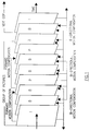
- FIGURE 1 shows three types of frames or pictures, "I” Intrapictures, "P” Predicted Pictures, and "B” Bidirectional Interpolated Pictures.
- the "I” Intrapictures provide moderate compression, and are access points for random access, e.g., in the case of video tapes or CD ROMS. As a matter of convenience, one "I” Intrapicture is provided approximately every half second. The "I” Intrapicture only gets information from itself. It does not receive information from an "P" Predicted Picture or "B” Bidirectional Interpolated Picture. Scene cuts preferably occur at "I" Intrapictures.
- P Predicted Pictures are coded with respect to a previous picture.
- P Predicted Pictures are used as the reference for future pictures, both "P" and "B” pictures.
- B Bidirectional Coded pictures have the highest degree of compression. They require both a past picture and a future picture for reconstruction. "B" bidirectional pictures are never used as a reference.
- the motion compensation unit under the MPEG-2 Draft Standard is the Macroblock unit.
- the MPEG-2 Draft Standard Macroblocks are 16x16 pixels.
- Motion information consists of one vector for forward predicted macroblocks, one vector for backward predicted macroblocks, and two vectors for bidirectionally predicted macroblocks.
- the motion information associated with each macroblock is coded differentially with respect to the motion information present in the reference macroblock. In this way a macroblock of pixels is predicted by a translation of a macroblock of pixels from a past or future picture.
- the difference between the source pixels and the predicted pixels is included in the corresponding bit stream.
- the decoder adds a correction term to the block of predicted pixels to produce the reconstructed block.
- each macroblock of a "P" Predicted Picture can be coded with respect to the closest previous "I” Intrapicture, or with respect to the closest previous "P” Predicted Picture.
- each macroblock of a "B" Bidirectional Picture can be coded by forward prediction from the closest past "I” or “P” Picture, by backward prediction from the closest future "I” or “P” Picture, or bidirectionally, using both the closest past "I” or “P” picture and the closest “future "I” or “P” picture.
- Full bidirectional prediction is the least noisy prediction.
- Motion information is sent with each macroblock to show what part of the reference picture is to be used as a predictor.
- motion vectors are coded differentially with respect to motion vectors of the previous adjacent block.
- Variable Length Coding is used to code the differential motion vector so that only a small number of bits are needed to code the motion vector in the common case, where the motion vector for a macroblock is nearly equal to the motion vector for a preceding macroblock.
- Spatial redundancy is the redundancy within a picture. Because of the macroblock based nature of the motion compensation process, described above, it was desirable for the MPEG-2 Draft Standard to use a block based method of reducing spatial redundancy. The method of choice is the Discrete Cosine Transformation, and Discrete Cosine Transform coding of the picture. Discrete Cosine Transform coding is combined with weighted scalar quantization and run length coding to achieve still further levels of compression.
- the Discrete Cosine Transformation is an orthogonal transformation. Orthogonal transformations, because they have a frequency domain interpretation, are filter bank oriented. The Discrete Cosine Transformation is also localized. That is, the encoding process samples on an 8x8 spatial window which is sufficient to compute 64 transform coefficients or sub-bands.
- Discrete Cosine Transformation Another advantage of the Discrete Cosine Transformation is that fast encoding and decoding algorithms are available. Additionally, the sub-band decomposition of the Discrete Cosine Transformation is sufficiently well behaved to allow effective use of psychovisual criteria.
- the Discrete Cosine Transformation encoding is carried out in the three stages as shown in FIGURE 2.
- the first stage is the computation of the Discrete Cosine Transformation coefficients.
- the second step is the quantization of the coefficients.
- the third step is the conversion of the quantized transform coefficients into ⁇ run-amplitude ⁇ pairs after reorganization of the data into zig-zag scanning order.
- Quantization enables very high degrees of compression, and a high output bit rate, and retains high picture quality.
- Quantization can be adaptive, with "I” Intrapictures having fine quantization to avoid “blockiness” in the reconstructed image. This is important because “I” Intrapictures contain energy at all frequencies. By way of contrast, “P” and “B” pictures contain predominantly high frequency energy and can be coded at a coarser quantization.
- the MPEG-2 Draft Standard specifies a layered structure of syntax and bit stream.
- the bit stream is separated into logically distinct entities to prevent ambiguities and facilitate decoding.
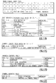
- the six layers are shown in Table 1, below Table 1 MPEG-2 Draft Standard Layers Layer Purpose Sequence Layer Random Access Unit and Context Group of Pictures Layer Random Access Unit and Video Coding Picture Layer Primary Coding Unit Slice Layer Resynchronization Unit Macroblock Layer Motion Compensation Unit Block Layer DCT Unit
- the digital signal decoder system of the invention is useful for receiving encoded compressed digital video signals and transmitting decoded digital video signals.
- the elements of the decoder system include a FIFO data buffer, a variable length code decoder, a dequantizer, a discrete cosine transform invertor, a motion compensator, a display unit video output, and a controller or controller.
- the FIFO Data Buffer receives compressed, encoded, digital video data from a cablecast or telecast network, another network, or an upstream apparatus or system, and temporarily stores the data, under control of the host processor, before transfer to memory.
- the system also includes a random access memory (RAM).
- the RAM which may be a SRAM, a DRAM, or a set of latches, serves two purposes.
- the RAM receives the compressed, encoded digital data for storage in a compressed, encoded Data Buffer that is connected to the FIFO Data Buffer.
- This portion of the RAM which may be a separate integrated circuit chip or chips, or incorporated into a single integrated circuit chip or chips, or main memory, is adapted to receive and store encoded compressed digital video data from the FIFO.
- the RAM also includes a data portion for storing decompressed decoded digital video pictures.
- a Memory Management Unit is provided for managing the RAM.
- the system includes a Variable Length Code Decoder, e.g., a Huffman decoder, for receiving encoded compressed data from the RAM. This data is received from the compressed, encoded Data Buffer portion of the RAM.
- the Variable Length Code Decoder provides a decoded bit stream for further processing.
- the system next includes an Inverse Quantizer for dequantizing the decoded data from the Variable Length Code Decoder.
- the Inverse Quantizer is characterized by several multiplication circuits where n-2 reduction is accomplished using (2,3,3) parallel counters.
- the system includes an Inverse Discrete Cosine Transform Decoder for transforming the dequantized, decoded data from the Inverse Quantizer from the frequency domain to the spacial domain in blocks of 8x8 pixel units.
- the system also includes a Motion Compensator for receiving Intrapictures and other information from the RAM, and error functions from the Inverse Discrete Cosine Transform Decoder, and forming motion compensated Predicted Pictures therefrom for return to the RAM.
- a Motion Compensator for receiving Intrapictures and other information from the RAM, and error functions from the Inverse Discrete Cosine Transform Decoder, and forming motion compensated Predicted Pictures therefrom for return to the RAM.
- the output of the system is through a Display Unit.
- the Display Unit provides an output of decoded, decompressed, motion compensated pictures from the RAM.
- the individual elements of the unit are under the control of a Controller or Controller.
- the Controller a Reduced Instruction Set Controller, with f-modulo add capability, controls the Memory Management Unit, the Variable Length Code Decoder, the Inverse Quantizer, the Inverse Discrete Cosine Transform Decoder, the Motion Compensator, and the Display Unit.
- the system can work with various downstream video elements, such as a digital computer, a television set, a recorder, or a network.
- the video decoder can be in combination with an audio decoder, separated therefrom by a suitable demultiplexer.
- the decoder system of the invention can be included in a stand-alone system, as a separate accessory, that is, a "set top box.”
- the decoder of the system can be integrally incorporated into the television set, computer, or other video device.
- the decoder can be integrated with a downstream element such as a digital computer, a television set, a recorder, or a network.
- the decoder system is incorporated on one or more printed circuit boards in the downstream element.
- the system of the invention can be in the form of a digital signal decoder system of a main memory and processor for receiving compressed encoded digital video signals and transmitting decompressed decoded digital video signals.
- the main memory has (1) a compressed, encoded Data Buffer adapted to receive and store encoded compressed digital video data, and (2) a data portion for storing decompressed digital video buffer, and a Memory Management Unit for managing the RAM.
- the decoder system can be a single integrated circuit chip having the FIFO Data Buffer, the Variable Length Code Decoder, the Inverse Quantizer, the Inverse Discrete Cosine Transform Decoder, the Motion Compensator, the Display Unit, and the Controller.
- an integrated circuit chip having the FIFO Data Buffer, the Variable Length Code Decoder, the Inverse Quantizer, the Inverse Discrete Cosine Transform Decoder, the Motion Compensator, the Display Unit, and the Controller.
- a complete digital video and audio entertainment system or a digital video and audio information system including the digital signal decoder system for receiving encoded compressed digital video signals and transmitting decoded decompressed digital video signals, for example to a consumer television set, a teleconferencing unit, a computer, or a redistribution network.
- the system includes main memory, the FIFO Data Buffer, the Variable Length Code Decoder, the Inverse Quantizer, the Inverse Discrete Cosine Transform Decoder, the Motion Compensator, the Display Unit, and the Controller, as well as an audio decoder unit and an output unit such as a television set, a recorder, a computer, or a network for rebroadcast.
- FIGURE 1 shows the three type of pictures and their relationship under the MPEG-2 Draft Standard, i.e., "I” Intrapictures, "P” Predicted Pictures, and "B” Birirectionally Predicted Pictures.
- FIGURE 2 shows the sequence of compressing a frame or picture, including calculating the Discrete Cosine Transform coefficients, quantizing the Discrete Cosine Transform coefficients, and "zig-zagging" the quantizied Discrete Cosine Transform coefficients.
- FIGURE 3 is a logical flow diagram showing the general logical flow of the MPEG-2 Draft Standard compliant decoder.
- FIGURE 4 is a block diagram of the functional units of the MPEG-2 Draft Standard compliant decoder of the invention.
- FIGURE 5 is a block diagram of the decode subsystem of the MPEG-2 Draft Standard compliant decoder of the invention.
- FIGURE 6 is a block diagram of the decoder of the invention in a dedicated or television set top box environment.
- FIGURE 7 is a block diagram of the decoder of the invention in a personal computer environment.
- FIGURE 8 is a representation of the front end bit stream logic located in the variable length decoder.
- FIGURE 9 is a representation of the controller.
- FIGURE 10 is a representation of the determination of bits read by the controller.
- FIGURE 11 is a representation of the hardware used for branching in the controller.
- FIGURE 12 is a representation of the operation of the Modulo Add with F-Code Range Adjustment.
- FIGURE 13 shows the IMMEDIATE word type format.
- FIGURE 14 shows the ADD word type format.
- FIGURE 15 shows the SPECIAL ARITHMETIC word type format.
- FIGURE 16 shows the SHIFT word type format.
- FIGURE 17 shows the READ SYMBOL word type format.
- FIGURE 18 shows the BRANCH word type format.
- FIGURE 19 shows the BRANCH RETURN word type format.
- FIGURE 20 shows the SYMBOL ADDRESS partition.
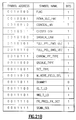
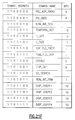
- FIGURES 21A, 21B, 21C, 21D, 21E and 21F show the symbol address table.
- FIGURE 22 is the logical diagram for the (2,3,3) parallel counter used in the Inverse Quantizer according to the invention.
- the systems, method, and apparatus of the invention receive encoded, compressed digital video data from a host interface bus, decompress and decode the digital video data, and deliver decompressed, decoded digital video data to a display interface, also referred to herein as a pixel bus. Conversion from digital data to analog data is done externally of the system, although in one embodiment, a digital to analog converter (DAC) can be incorporated into the system downstream of the pixel bus.
- DAC digital to analog converter
- the decoder system complies fully with the Moving Picture Experts Group MPEG-2 Draft Standard Main Profile at the Main Level, as defined in the MPEG documentation.
- the system can receive compressed video data at a rate of 15 Mbs/second, and the system can operate at a 40 MHz clock frequency.
- the data format for the compressed, encoded data is YCbCr (4:2:0).
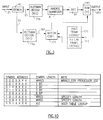
- FIGURE 3 shows the general internal data flow of the system of the prior art to support the MPEG-2 Draft Standard.
- the compressed, encoded data input 31 goes to a demultiplexer 41 where it is demultiplexed into two streams 51 and 61.
- Stream 61 goes to a Variable Length Code (VLC) Huffman Decoder 71b for decoding, and to an Inverse Quantizer 81 for dequantizing.
- VLC Variable Length Code
- IDC Inverse Discrete Cosine Transform
- the second data stream 51 also goes through a Variable Length Code (VLC) Huffman Decoder 71a where it is decoded into error functions 101 which go to a Motion Compensator 131.
- VLC Variable Length Code
- the Huffman Decoders 71a and 71b are shown as logically separate and distinct, although they may structurally and electronically the same element.
- the Motion Compensator 131 also receives a data stream derived from the first data stream 61 and the motion compensated data stream, summed in Summer 141.
- the output 151 of the Summer 141 goes to the pixel bus (not shown) and to storage, i.e., Future Frame Storage 111 and Past Frame Storage 121.
- the contents of the Future Frame Storage 111 and Past Frame Storage 121 are, as appropriate, inputs to the Motion Compensator 131.
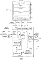
- FIGURE 4 shows the block diagram of the decoder system 201 of the invention.
- the system I/O includes three busses from the host interface 202 and two busses to the display interface 208.
- the buses from the host interface 202 include the data bus 203, the address bus, 205, and the control bus, 207.
- the data bus 203 may be a 16 bit or a 32 bit bus, or of some other width, and it may be bidirectional or unidirectional.
- the address bus 205 is a 6 bit bus, although other widths may be accommodated without departing from the invention.
- the control bus 207 is a 7 bit bus, although other widths may be accommodated without departing from the invention.
- the display interface 208 busses are the data bus 209 and the control bus 211.
- the data bus 209 is for pixel data.
- the control bus 211 is for synchronization and control.
- the system includes a host bus control element 231, a FIFO buffer 241, a decode subsystem 301, a controller 401, an instruction storage unit 402, a display bus control 501, and a Memory Management Unit 600.
- the memory includes a Compressed Data Buffer 611 for receiving data from the host interface 202 via the FIFO buffer 241, and frame buffers 621, 623, and 625, for receiving and storing decoded frames, including future frames and past frames.
- a Compressed Data Buffer 611 for receiving data from the host interface 202 via the FIFO buffer 241, and frame buffers 621, 623, and 625, for receiving and storing decoded frames, including future frames and past frames.
- the interface between the memory management unit 600 and the memory 601 includes an address bus, 221, a bidirectional data bus, 223, and a control bus 225.
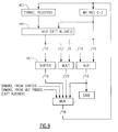
- the decode unit 301 shown with detail in FIGURE 5, consists of functional units that operate under the control of the controller 401 and its associated Instruction Storage Unit 402. These decode functional units include the Variable Length Code Huffman Decoder 311, the Inverse Quantizer or Dequantizer, 321, the Inverse Discrete Cosine Transform unit, 331, and the Motion Compensation Unit, 341.
- the controller 401 is the central point of control for the decoder.
- the controller 401 microcode is stored in an Instruction Storage unit 402.
- the controller 401 interacts with the host system through an external processor through the host or system bus for high level commands and status.
- the controller 401 is responsible for the control and command of the other functional elements, as well as providing global synchronization of these units.
- the controller 401 is coupled to the Variable Length Code Huffman Decoder 311. This enables parsing of the code stream. Parsing of the code streams and processing of header information is done by the controller 401 interacting with the VLC Huffman Decoder 311.
- the Variable Length Code Huffman Decoder 311 contains tables for decoding the data stream and a local state machine that controls the decoding of run/level data for macroblocks.
- the VLC 311 is controlled by the controller 401 as header information and block run/level symbols are passed from the compressed bit stream.
- a local state machine decodes the run/level symbols and interacts with the Inverse Quantizer 321 to process the decoded signals.
- variable length coding e.g., Huffman coding
- Huffman coding is a statistical coding technique that assigns codewords to symbols. Symbols with a high probability of occurrence are assigned short codewords, while symbols with a low probability of occurrence are assigned longer codewords.
- the codes used in the MPEG-2 VLC decoder are taken from the MPEG-2 Draft Standard.
- the codes form a class of codes known as prefix codes.
- prefix codes In a prefix code system, no valid code is a prefix of another code.
- the number of bits assigned to each codeword is variable, from a minimum of 1 to a maximum of 16.
- the coded bits used to represent a sequence of symbols are a variable length string of bits. This bit string must be decoded sequentially in order to reconstruct the original sequence of symbols.
- Huffman coding generates code tables based on symbol occurrence probabilities.
- the codes generated are minimum redundancy codes.
- the Huffman coding used by the MPEG-2 Draft Standard is based on a static coding algorithm.
- the coding procedure used by Huffman Coding is lossless coding, because the exact sequence of symbols encoded is recovered by the decoding process.
- the Inverse Quantizer 321 receives run/level (run/amplitude) coded symbols from the VLC unit 311 and outputs a block of 64 coefficients that are sent to the Inverse Discrete Cosine Transform Unit 331.
- the Inverse Quantizer 321 converts the run/level coded symbols to zeros and symbols, unzigs the data, handles differential pulse code modulation (DPCM) decoding for the Discrete Cosine coefficients, and dequantizes the data.
- DPCM differential pulse code modulation
- FIGURE 2 shows the zig-zag scanning order of the Discrete Cosine Transform coefficients.
- the top left coefficient is the DC coefficient. All other coefficients are considered as AC terms.
- the numbers indicate the order in which the coefficients are read for run length and level coding.
- the process after run length coding is to "unzig" the data. This means placing the "level” data in the correct positions relative to an 8 by 8 block or matrix.
- the "run” identifies the number of skipped positions, i.e., zeros.
- the levels also need to be further processed under quantization.
- quantization that is, in encoding
- the level is divided by a number called the "quantization factor” to become a quantized coefficient.
- Quantization and dequantization introduce some degree of loss into the decoded data.
- the unzigged quantized coefficient (“level”) will be multiplied by the quantization factor to produce a dequantized coefficient.
- This coefficient a frequency domain value, will go to the Inverse Discrete Cosine Transform unit 331 to be transformed back to a time domain based signal.
- Intra blocks also known as I-Pictures or as I-frames, contain DC coefficients that are Differential Pulse Code Modulation coded. This means that the DC value of the previous value predicts the current 8 by 8 block DC value. The quantized difference is then coded.
- the Differential Pulse Code Modulation coding for the DC coefficient is applicable for all three components, i.e., the Y component, the Cb component, and the Cr component. After Differential Pulse Code Modulation decoding, the DC coefficients of the 8 by 8 block will go through the inverse quantization process before being sent to the Inverse Discrete Cosine Transform unit 331.
- the Inverse Quantization can utilize multiplication circuits using (2,3,3) parallel counters.
- multiplication occurs in three stages.
- the first stage requires generation of partial product terms.
- the second stage sums the partial products from N bits to 2 bits.
- the third stage adds the final two bits per bit position via a carry look ahead adder to achieve the final numerical result.
- the total delay of a multiplication is the sum of the delays of all three stages.
- the second stage, summing the partial products from N bits to 2 bits, has the longest delay.
- the sum of the three stages must also shorten in order for the multiplication of two numbers to occur within a single clock cycle. This is especially true for the inverse quantizer, which is a multiplication intensive step.
- the (2,3,3) parallel counter used in the inverse quantizer has the logical structure shown in FIGURE 22, and represented by the Boolean terms:
- the Inverse Discrete Cosine Transform unit 331 After a block of signals have been dequantized in the Dequantizer unit 321 the Inverse Discrete Cosine Transform unit 331 performs a two dimensional inverse discrete cosine transform on the 8 by 8 block to form a reconstructed image block. The reconstructed image block is added to the predicted block from the Motion Compensation Unit 341 if required. The Inverse Discrete Cosine Transform Unit 331 and the Motion Compensation Unit 341 synchronize their outputs during this summation step. The summation results are then sent to the memory 601 for output to display and for reference.
- the Motion Compensation Unit 341 receives commands and address from the controller 401 and performs the required interpolations to form predicted image blocks.
- the predicted output block is synchronized to the output of the Inverse Discrete Cosine Transform and added to the output of the Inverse Discrete Cosine Transform reconstructed block by this summation step.
- Motion compensation exploits the temporal redundancy in video pictures by coding the difference between a current block and a block in a previous picture or in a future picture. Motion within a picture means the pels will be in a different location than in the reference picture. This displacement is given by motion vectors. These motion vectors and the coded difference between the current and the future picture construct the motion compensated picture.
- Motion compensation includes prediction from past, or future, or both past and future pictures, utilizing motion pels of full pel or half pel accuracy. Motion compensation is carried out in both interlaced and non-interlaced video data streams.
- the decoder system of the invention is shown in a dedicated, digital entertainment terminal environment in FIGURE 6.
- the system receives input from the cable or upstream broadcasting means 651. This is demultiplexed into video, audio, and ASCII portions in demultiplexer 661.
- the system includes the video decoder 11 of the invention, an audio decoder 21, an ASCII Generator 31, and an Infrared Receiver 41.
- the ASCII Generator 31, the Audio Decoder 41, and the Video Decoder 11 provide outputs through the NTSC (National Television Standards Committee) generator 51.
- NTSC National Television Standards Committee
- the compressed video data input comes from either a storage device or a network communications adapter.
- the video data is typically handled as a packet transfer across a system I/O bus. This means that the system of the invention must be capable of receiving bursts of data at high rates for a limited time, and then allow other devices to use the system I/O bus while the encoded data is being processed. This is accomplished through the use of the internal FIFO buffer 241 which must be large enough to handle such data bursts.
- the decompressed video data stream is provided on the display (Pixel Bus) Interface, which can directly interface to a video controller. Alternatively, the video data stream can be sent on a high bandwidth system bus to a graphics processor frame buffer.
- FIGURE 7 A typical PC system environment is shown in FIGURE 7.
- the FIGURE shows the system bus 701, with various system bus subsystems, e.g., a network adapter 703, a SCSI adapter 705, a system memory 707, and a host processor 709.
- the system of the invention is connected to the system bus 701 through a graphics adapter card 711 and includes a digital signal processor 713, the decoder 201 of the invention, DRAM 601, and SRAM 602
- the Graphics Adapter Card 711 provides interface to an optional Display Daughter Card 715, to a Graphics Display 717, or to both.
- the system has three external interfaces, a host interface 202, a display interface 208, and a memory interface 221, 223, 225.
- the host interface 202 is the primary control and compressed data interface.
- This interface 202 a 16 bit slave interface, provides host processor, i.e., transmission network, access to the internal registers, local storage, and functional units of the system.
- the Host Interface 202 functions as the command, status, and encoded data interface for the system. High level systems commands and status are passed between the decoder system of the invention and the host system through this host interface 202.
- the host interface 202 provides a generic interface protocol to the host, that appears as a register port interface.
- the host interface 202 includes the address, data, and control pin out.
- the pin outs include address, data, chip select, write pulse, output enable, FIFO buffer full, system clock, timer clock, and reset.
- the chip select pin indicates that the chip is being selected for register access.
- the write pulse is an instruction to either receive data from the host or write data to the host.
- Output Enable is used to tristate the Host data bus, allowing the chip to drive the host data bus.
- FIFO Buffer Full is only used for dynamic, synchronous operation, as in a PC environment.
- the System clock is an oscillator that provides timing for the internal processor and operations. This clock does not affect the Host Interface control signals which are asynchronous with respect thereto.
- the timer clock is an externally generated clock signal that synchronizes the video with the audio.
- Reset is a power on reset signal.
- the host bus carries signals that initialize the decoder, by resetting the chip, setting the chip mode, setting display parameters, loading Display Instruction Storage, starting the decoder processor, loading compressed data into the FIFO buffer, setting the system clock reference, and starting the decoder.
- the Memory Interface supports direct attachment to a local memory that stores multiple frames of decompressed video data, partially decoded pictures, and compressed input data. Reference pictures used for motion compensation are stored in External Memory 601. The system input is stored in a compressed data buffer 611, which may be part of the External Memory 601. The compressed data buffer 611 is loaded from the host bus interface 202 and read into the Variable Length Coder 311 under the control of the controller 401.
- the Display or Pixel Bus Interface 208 is the primary interface for passing decompressed video image data to a downstream unit, such as a display unit, or a graphics interface card, that will ultimately be responsible for displaying the video.
- This consists of 16 bits of pixel data output, and control inputs FLDID, the field ID; PCLK, the Pixel Clock; CB, the composite blank, which indicates the inactive portion of each line; and POE, the Pixel Output Enable, generated externally and used by the decoder to control the drivers to the output.
- the controller 401 controls the functional elements of the decoder system 201.
- the controller 401 is a Reduced Instruction Set Controller element with a minimal instruction set. In a preferred embodiment it is formed of a CMOS standard cell integrated circuit chip, although other implementations may be used. Critical to the controller is the minimal instruction set described herein with branching to match the MPEG-2 Draft Standard layers.
- Video decompression standards such as the MPEG-2 Draft Standard, utilize a video decoder to receive an encoded, compressed, serial bit stream, and translate the encoded, compressed serial bit stream into a sequence of moving pictures.
- the syntax of the bit stream is hierarchical, using a layered structure to define decoding parameters to be used for an entire sequence, for a group of pictures, for an individual picture or pictures, and for the motion vectors.
- the MPEG-2 Draft Standard syntax allows many possibilities of encoding techniques, and allows for extensions to the syntax itself for future changes. Therefore, a video decoder must be flexible enough to allow reception of these various types of streams, while being very cost competitive.
- a specialized controller 401 controls a specialized decompression and decoding system 201 of the invention.
- the controller 401 reads out each parameter from the encoded, compressed bit stream, in real time, and makes decisions upon the decoding at every level of the architecture.
- the controller 401 allows the use of a limited set of instructions, i.e., a reduced instruction set, in order to keep the decoding system small and cost effective.
- the controller 401 provides a Read Symbol Instruction that provides direct read control from the encoded bit stream. This allows fast processing since the Read Symbol Instruction works closely with the rest of the system in reading the bit stream in real time while simultaneously being able to make decisions within the execution cycle without further bit or character tests to achieve the flexibility necessary for supporting the MPEG-2 Draft Standard syntax.
- the controller 401 also has Fast Branching control for the Read Symbol Instruction. This allows specialized decision making based upon the current parameter being read out of the encoded, compressed bit stream.
- the controller 401 also has Modulo-Add with F code adjustment. This reduces the software steps for motion vector calculations.
- the encoded, compressed bit stream consists of a concatenation of parameters. Many of these parameters are represented by a variable length code (VLC).
- VLC variable length code
- the variable length code requires translation to an expanded number of bits.
- the parameters are grouped together and separated by start bits, which are code points that have a fixed number of zeros preceding some unique value.
- the start codes separate the layers and extensions in the encoded video standard, i.e., the MPEG-2 Draft Standard.
- the controller 401 participates in the read of every parameter that is presented.
- the front end bit stream logic located in the VLC is shown in FIGURE 8. Hardware is used to feed the encoded bit stream from the memory, into a FIFO buffer 411, and then into registers 413 and 415 in order for the controller 401 to perform the Read Symbol Instruction.
- the left shifter 421 allows the controller 401 to see the most recent 16 bits of the bitstream left justified. The bit stream is otherwise unmodified.
- the controller 401 receives either (1) the output of the shifter 421, or (2) the decoded value of the shifter output.
- the decoded value of the shifter output is obtained from the VLC decoder by VLC tables.
- the output of the shifter 421 goes through a multiplexer and the result is placed in a symbol register 451 , shown in FIGURE 9.
- Determination of the number of bits read from the encoded bit stream is accomplished by a length field in the instruction, by the address of the register, or by the VLC decoder . This becomes the code length, which is used by the shifter 421 to position the next parameter in the bit stream so that it is now left justified for the controller 401.
- FIGURE 10 shows how this address can be used to determine the number of bits that have been read.
- the power of the Read Symbol Instruction is further enhanced by giving it the capability of performing decisions based upon the status of the current parameters in the bit stream. This is accomplished through the Continue, Stay, or Skip branching control.
- CONTINUE means to execute the current instruction and then go onto the next instruction.
- STAY means to repeat the same instruction until a condition is true.
- SKIP means to execute the current instruction and if a condition is true, bypass the next sequential instruction and execute the one that follows.
- STAY allows reduction of the number of instructions when it is necessary to read out a large block of parameters. There is no need to insert test and branch instructions in a loop. The loop can be accomplished in a single word. The loop is broken by the condition changing from false to true as parameters are read out.
- SKIP allows conditional branching without the insertion of additional test and branch instructions. The condition itself forces the branch.
- FIGURE 11 shows the hardware used to perform branching.
- the instructions are read in an Instruction Storage Unit 402, and the next instruction is addressed by the CS_ADDR register 473.
- the normal increment of the CS_ADDR register 473 can be overridden by the branch condition caused by the execution of the Read Symbol Instruction.
- the Modulo Add With F-Code Range Adjustment is a special function designed to minimize the number of instructions necessary for motion vector calculation.
- the F-Code is a parameter from the encoded bit stream. It specifies a range of bits to be used in the motion vector calculation. Once it is read into a register as a symbol, the F-Code is used by the system to modify the position of the most significant bit during addition. This eliminates the need for software to do shifts, back and forth, during time critical calculations. This is illustrated in FIGURE 12.
- Immediate commands allow direct control of hardware units.
- a specific command can be presented to all hardware units, with only one hardware unit recognizing the command.
- the command can be sent to the hardware using the immediate instruction type, with the constant field being one out of a possible sixty four specific commands. This permits the software to have additional control and/or flexibility in carrying out the decode process.
- the controller 401 has seven word types, an IMMEDIATE word type, an ADD word type, a SPECIAL ARITHMETIC word type, a SHIFT word type, a READ SYMBOL word type, a BRANCH word type, and a BRANCH RETURN word type.
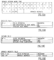
- the word types are identified by bits 0-2 thereof. This is shown in Table 2, below.
- FIGURE 13 shows the IMMEDIATE word type command format, with the function field ⁇ Bits 3-4 ⁇ , a Low Byte Field ⁇ Bit 5 ⁇ , a Working Register Address Field ⁇ Bits 6-7 ⁇ when the Function Field is not indicating a Load Command, and a Command Type Field ⁇ Bits 6-7 ⁇ when the Function Field ⁇ Bits 3-4 ⁇ is indicating a Load Command. Bits ⁇ 8-15 ⁇ carry a constant.
- the IMMEDIATE word allows an 8 bit constant to be applied to a Work Register by either a direct loading or a logical function.
- the Work Field Register is used to indicate which work register is to be used in the operation.
- the work register field indicates which work register is the destination.
- the work register field is used as the source. The result of a logical function is always destined to Work Register 0.
- the constant is only 8 bits wide, while the work registers are 16 bit registers.
- the High/Low field, bit 5 indicates which byte the constant should operate on, and which byte of the result should be destined. When the bit is 0 the high order byte is used, and when the bit is 1 the operation is on the low order byte.
- bits 3-4 When the Function field, bits 3-4, indicates a Load Command operation, i.e., when bits 3-4 equal 11, the work field register is used to indicate the command type.
- FIGURE 14 shows the ADD word type command format, with a 001 in bits 0-2, a Subtract field in bit 3, and a Carry-In Control field in bits 4-5.
- the Work Register Address field is bits 6-7 when the Carry In Control is not a Special Add, and controls Increment By 1 and Decrement By 1 when the Carry In Control field is a Special Add.
- Bit 8 is a Destination Field, and bits 9-15 are the Symbol Address.
- the ADD word performs addition or subtraction on two 16-bit operands.
- the A-operand is indicated by the Symbol Address Field, bits 9-15
- the B-operand is indicated by the Work Register field, bits 6-7.
- the result is always destined to Work Register 0 if the bit in the destination field is 0. If the bit in the Destination Field is 1, the Symbol Address field, bits 9-15, is used as a destination address as well as a source address.
- the Subtract field indicates whether a subtraction is to be performed. When bit 3 is 0, an addition is performed. When bit 3 is 1, a subtraction is performed. The subtraction is performed by inverting the B-operand before the hard wired addition is performed.
- the Carry In Control, bits 4-5, is used to perform 2's complement subtraction and addition of numbers more then 16 bits if needed. When performing a two's complement subtraction, the carry in is set to 1. When adding two 32 bit numbers the lower 16 bits are added first. The carry-out is saved and used as the carry for the high order 16 bit add.
- the adder can add a 16 bit value to the 20 bit symbol and destine the result to a 20 bit symbol. If the result is destined to a 16 bit register, then the high order four bits are lost.
- the ADD word also performs the "increment by 1" and "decrement by 1" functions.
- the Carry In Control field is 11
- the Work Register field is used to indicate the special add functions, i.e., Increment by 1 or Decrement by 1.
- the selected symbol register is either incremented by 1 or decremented by 1, depending on the special add function.
- FIGURE 15 shows the SPECIAL ARITHMETIC Word Type command format. This is a powerful command. Bits 3-5 are the Function field, and control such functions as Clear, Move, Load Positive, Load Negative, Multiply, and Modulo Add. Bits 6-7 indicate the work register. Bit 8 indicates the destination. Bits 9-15 indicate the Symbol Address field.
- the SPECIAL ARITHMETIC WORD performs special arithmetic operations. If the operation is a single operand operation, the source operand is the Symbol Address or the work register. When the bit in the destination Field is 0, the Symbol Address Field indicates the source operand and the Work Register field selects the destination register. If the bit is 1, the Work Register is used as the source and the Symbol Address identifies the register to be destined.
- the Special Arithmetic Word can call the functions CLEAR REGISTER, MOVE, LOAD POSITIVE, LOAD NEGATIVE, MULTIPLY, and F-CODE MODULO ADD.
- CLEAR REGISTER clears the register specified by the symbol address or work register address. If the destination bit is 0 the register selected by the work register is set to 0. If the destination bit is 1, the symbol address selects the register to be cleared.
- MOVE transfers contents between registers.
- MOVE moves the contents from the register selected by the symbol address to the work register selected by the work register field.
- MOVE moves the contents from the register selected by the work register field to the register selected by the symbol address field.
- LOAD POSITIVE changes the source operand to a positive number if it is negative, but leaves the operand unchanged if it is positive.
- the result is destined to the selected register.
- the symbol register field or the work register field can be the destination address, depending on the setting of the destination bit.
- LOAD NEGATIVE changes the source operand to a negative number if it is positive, but leaves the operand unchanged if it is negative.
- the result is destined to the selected register.
- the symbol register field or the work register field can be the destination address, depending on the setting of the destination bit.
- MULTIPLY performs a 12 bit by 8 bit 2's-complement multiply.
- the 12 bit input comes from the register selected by the symbol address and the 8 bit input is from the work register. If the destination register is less than 20 bits, the high order bits, if any, will be lost. The result can be destined to either the symbol register or the work register, depending on the destination bit.
- the multiply utilizes the (2,3,3) parallel counter.
- F-MODULO ADD performs addition and propagates the sign bit selected by the f-code.
- the A-input to the adder is from the symbol address and the B-input is from the work register address.
- the result can be destined to either the symbol register or the work register depending on the destination bit. This function is used when adding the calculated motion vector to the previous motion vector.
- FIGURE 16 shows the SHIFT Word Type command format.
- Bit 3 is the right shift field, differentiating between a right shift and a left shift.
- Bits 4 to 7 are the Shift Amount Field.
- Bit 8 is the destination Field.
- Bits 9 to 15 are the Symbol Address Field.
- SHIFT performs the left or right shift on the operand indicated by the Symbol Address field by the number of bits indicated by the Shift Amount field.
- the destination field is used to indicate whether the Symbol Address is also used for destination. When the bit is 0, the result is always destined for Work Register 0. When it is 1, the result is destined to the register indicated by the Symbol Address. This allows data in a register to be shifted without an additional word. If the shift amount, bits 4-7, is set to 0, the 4 bits of the Shift Indirect register are used as the shift amount.
- the shifter can source a 20-bit register and the result to another register. If the destination is only 16 bits wide, the high order 4 bits are lost. The shift amount is limited to 15.
- FIGURE 17 shows the READ SYMBOL WORD Type command format.
- Bits 3-6 can be the Fast Branch Condition Field (Branch Control bits 7-8 unequal 11) or the Symbol Length Field (Branch Control bits 7-8 equal 11).
- Bits 7-8 are the branch control field.
- Bits 9-15 are the Symbol Address Field.
- the command performs a logical shift except when it is a right shift, and the shift amount is 1, in which case an arithmetic shift is performed.
- This function is used to do a division by 2.
- READ SYMBOL WORD parses the coded bit stream. While processing header information, symbols are read from the output of the bit stream shifter and destined to the symbol register indicated by the Symbol Address field.
- the Symbol Address also implies the length of the symbol if it is a fixed length symbol. If the symbol is a variable length coded symbol, the length is generated from the VLC tables. The length is used to update the pointer which is used to control the bit stream shifter. While processing run/level information, a symbol is read from the output of the bit stream shifter and destined to the symbol decoding pipeline.
- Branch Control allows the word to be repeated until the branch condition is met. It also controls the conditional skip so that the execution of the next word can be avoided.
- the Fast Branch Condition field becomes the length of the symbol to be read.
- the variable length code (VLC) hardware will use the length to control the bit stream shifter. The length implied by the symbol address is ignored. Under this condition the Branch Control defaults to Continue.
- the fast branch controls include: CONTINUE (tells the control store to move onto the next sequential microword); STAY UNTIL CONDITION (this decode allows the instruction to be repeated many times until the condition is met; the fast branch condition is used to block the setting of the control store address and the control register); and SKIP ON CONDITION (this decode "no-ops" the execution of the next instruction if the branch condition is met).
- FIGURE 18 shows the BRANCH Word Type command format.
- Bit 3 is the Execute Field, and is 0 for a Branch (no execute on next word) and 1 for an execute on next word.
- Bits 4 to 6 are the Branch Condition Field.
- Bits 7 to 15 are the Branch Address Field.
- BRANCH WORD performs a branching within a 512 word range.
- the instruction storage address is set to the address indicated by the Branch Address field.
- the Execute bit is 1, the word following the branch word will be executed while the branch target is being accessed.
- the bit is 0, and the branch is successful, a dead cycle is introduced due to the lack of an instruction before the execution is resumed.
- FIGURE 19 shows the BRANCH RETURN word type. Bit 3 is the Execute field. Bit 4 is the Return field. Bits 5 and 6 are don't care bits. Bits 7 to 15 are the Branch Address Field.
- BRANCH_RETURN performs a branching to a subroutine by the branch address and returns to the address following the Branch Return when a Return is specified in the subroutine.
- an Execute bit is included in the word. When the Execute Bit is 1, the word following the branch word will be executed while the branch target is being accessed. When the Execution bit is 0, execution is inhibited, and a dead cycle is introduced for accessing the branch target.
- the address for the word following the BRANCH RETURN word is saved in the CSAR Save register. This address is loaded into the Control Store Address register 473 when executing a Branch Return word with the Return bit set to 1.
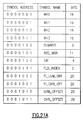
- FIGURE 20 shows the Symbol Address Partition
- FIGURES 21A, 21B, 21C, 21D, and 21E are the Symbol Address Table.
- a digital signal decoder system for receiving encoded digitized video signals and transmitting decoded digital video signals, said decoder system having a RAM with
- a digital entertainment system comprising a digital signal decoder system for receiving encoded digitized video signals and transmitting decoded digital video signals, said decoder system comprising:
Abstract
Description
- This invention relates to video decoders, especially video decoders intended to decode and decompress compressed encoded video signals, e.g., discrete cosine transform encoded video signals. The method, apparatus, and system of the invention are useful in decoding broadcast signals, cablecast signals, and digital network signals, as well as in high definition television, interactive television, multimedia, video on demand, video conferencing, and digital video recording. The system and apparatus of the invention may be a "stand alone" unit, as a set top box or a digital entertainment terminal, or the like, as a component of a television set, a personal computer, work station, or other computer, as a unit contained on one or more printed circuit boards, or as part of a video recorder or dedicated teleconferencing unit.
- The Moving Picture Experts' Group (MPEG) MPEG-2 Draft Standard is a compression/decompression standard for interactive video applications. The standard describes an encoding method that results in substantial bandwidth reduction by a subjective lossy compression followed by a lossless compression. The encoded, compressed digital video data is subsequently decompressed and decoded in an MPEG-2 Draft Standard compliant decoder.
- The MPEG-2 Draft Standard is described in, e.g., C.A. Gonzales and E. Viscito, "Motion Video Adaptive Quantization In The Transform Domain," IEEE Trans Circuits Syst Video Technol,
Volume 1, No. 4, Dec. 1991, pp. 374-378, E. Viscito and C.A. Gonzales, "Encoding of Motion Video Sequences for the MPEG Environment Using Arithmetic Coding," SPIE, Vol. 1360, pp. 1572-1576, (1990), D. LeGall, "MPEG: A Video Compression Standard for Multimedia Applications," Communications of the ACM, Vol. 34, No. 4, (April 1991), pp. 46-58, S. Purcell and D. Galbi, "C Cube MPEG Video Processor," SPIE, v. 1659, (1992) pp. 24-29, and D. J. LeGall, "MPEG Video Compression Algorithm," Signal Process Image Commun, v. 4, n. 2, (1992), pp. 129-140, among others. - The MPEG-2 Draft Standard specifies a very high compression technique that achieves compression not achievable with intraframe coding alone, while preserving the random access advantages of pure intraframe coding. The combination of frequency domain intraframe encoding and interpolative/predictive interframe encoding of the MPEG-2 Draft Standard result in a balance between intraframe encoding alone and interframe encoding alone.
- The MPEG-2 Draft Standard exploits temporal redundancy for motion compensated interpolative and predictive encoding. That is, the assumption is made that "locally" the current picture can be modelled as a translation of the picture at a previous and/or future time. "Locally" means that the amplitude and direction of the displacement are not the same everywhere in the picture.
- MPEG-2 Draft Standard specifies predictive and interpolative interframe encoding and frequency domain intraframe encoding. It has block based motion compensation for the reduction of temporal redundancy, and Discrete Cosine Transform based compression for the reduction of spatial redundancy. Under MPEG-2 Draft Standard motion compensation is achieved by predictive coding, interpolative coding, and Variable Length Coded motion vectors. The information relative to motion is based on a 16x16 array of pixels and is transmitted with the spatial information. It is compressed with Variable Length Codes, such as Huffman codes.
- The MPEG-2 Draft Standard provides temporal redundancy reduction through the use of various predictive and interpolative tools. This is illustrated in FIGURE 1. FIGURE 1 shows three types of frames or pictures, "I" Intrapictures, "P" Predicted Pictures, and "B" Bidirectional Interpolated Pictures.
- The "I" Intrapictures provide moderate compression, and are access points for random access, e.g., in the case of video tapes or CD ROMS. As a matter of convenience, one "I" Intrapicture is provided approximately every half second. The "I" Intrapicture only gets information from itself. It does not receive information from an "P" Predicted Picture or "B" Bidirectional Interpolated Picture. Scene cuts preferably occur at "I" Intrapictures.
- "P" Predicted Pictures are coded with respect to a previous picture. "P" Predicted Pictures are used as the reference for future pictures, both "P" and "B" pictures.
- "B" Bidirectional Coded pictures have the highest degree of compression. They require both a past picture and a future picture for reconstruction. "B" bidirectional pictures are never used as a reference.
- Motion compensation goes to the redundancy between pictures. The formation of "P" Predicted Pictures from "I" Intrapictures and of "B" Bidirectional Coded Pictures from a pair of past and future pictures is a key feature of the MPEG-2 Draft Standard technique.
- The motion compensation unit under the MPEG-2 Draft Standard is the Macroblock unit. The MPEG-2 Draft Standard Macroblocks are 16x16 pixels. Motion information consists of one vector for forward predicted macroblocks, one vector for backward predicted macroblocks, and two vectors for bidirectionally predicted macroblocks. The motion information associated with each macroblock is coded differentially with respect to the motion information present in the reference macroblock. In this way a macroblock of pixels is predicted by a translation of a macroblock of pixels from a past or future picture.
- The difference between the source pixels and the predicted pixels is included in the corresponding bit stream. The decoder adds a correction term to the block of predicted pixels to produce the reconstructed block.
- As described above and illustrated in FIGURE 1, each macroblock of a "P" Predicted Picture can be coded with respect to the closest previous "I" Intrapicture, or with respect to the closest previous "P" Predicted Picture.
- Further, as described above and illustrated in FIGURE 1, each macroblock of a "B" Bidirectional Picture can be coded by forward prediction from the closest past "I" or "P" Picture, by backward prediction from the closest future "I" or "P" Picture, or bidirectionally, using both the closest past "I" or "P" picture and the closest "future "I" or "P" picture. Full bidirectional prediction is the least noisy prediction.
- Motion information is sent with each macroblock to show what part of the reference picture is to be used as a predictor.
- As noted above, motion vectors are coded differentially with respect to motion vectors of the previous adjacent block. Variable Length Coding is used to code the differential motion vector so that only a small number of bits are needed to code the motion vector in the common case, where the motion vector for a macroblock is nearly equal to the motion vector for a preceding macroblock.
- Spatial redundancy is the redundancy within a picture. Because of the macroblock based nature of the motion compensation process, described above, it was desirable for the MPEG-2 Draft Standard to use a block based method of reducing spatial redundancy. The method of choice is the Discrete Cosine Transformation, and Discrete Cosine Transform coding of the picture. Discrete Cosine Transform coding is combined with weighted scalar quantization and run length coding to achieve still further levels of compression.
- The Discrete Cosine Transformation is an orthogonal transformation. Orthogonal transformations, because they have a frequency domain interpretation, are filter bank oriented. The Discrete Cosine Transformation is also localized. That is, the encoding process samples on an 8x8 spatial window which is sufficient to compute 64 transform coefficients or sub-bands.
- Another advantage of the Discrete Cosine Transformation is that fast encoding and decoding algorithms are available. Additionally, the sub-band decomposition of the Discrete Cosine Transformation is sufficiently well behaved to allow effective use of psychovisual criteria.
- After transformation, many of the frequency coefficients are zero, especially the coefficients for high spatial frequencies. These coefficients are organized into a zig-zag, as shown in FIGURE 2, and converted into run-amplitude (run-level) pairs. Each pair indicates the number of zero coefficients and the amplitude of the non-zero coefficient. This is coded in a Variable Length Code.
- Discrete Cosine Transformation encoding is carried out in the three stages as shown in FIGURE 2. The first stage is the computation of the Discrete Cosine Transformation coefficients. The second step is the quantization of the coefficients. The third step is the conversion of the quantized transform coefficients into {run-amplitude} pairs after reorganization of the data into zig-zag scanning order.
- Quantization enables very high degrees of compression, and a high output bit rate, and retains high picture quality.
- Quantization can be adaptive, with "I" Intrapictures having fine quantization to avoid "blockiness" in the reconstructed image. This is important because "I" Intrapictures contain energy at all frequencies. By way of contrast, "P" and "B" pictures contain predominantly high frequency energy and can be coded at a coarser quantization.
- The MPEG-2 Draft Standard specifies a layered structure of syntax and bit stream. The bit stream is separated into logically distinct entities to prevent ambiguities and facilitate decoding. The six layers are shown in Table 1, below
Table 1 MPEG-2 Draft Standard Layers Layer Purpose Sequence Layer Random Access Unit and Context Group of Pictures Layer Random Access Unit and Video Coding Picture Layer Primary Coding Unit Slice Layer Resynchronization Unit Macroblock Layer Motion Compensation Unit Block Layer DCT Unit - It is one object of the invention to provide a system that increases the speed of the decoding process.
- It is another object of the invention to provide an integrated decoder system that can be incorporated in other video and entertainment products.
- It is still another object of the invention to reduce the clock cycles required for decoding a picture.
- These and other objects of the invention are attained by the digital signal decoder system of the invention. The system is useful for receiving encoded compressed digital video signals and transmitting decoded digital video signals. The elements of the decoder system include a FIFO data buffer, a variable length code decoder, a dequantizer, a discrete cosine transform invertor, a motion compensator, a display unit video output, and a controller or controller.
- The FIFO Data Buffer receives compressed, encoded, digital video data from a cablecast or telecast network, another network, or an upstream apparatus or system, and temporarily stores the data, under control of the host processor, before transfer to memory.
- The system also includes a random access memory (RAM). The RAM, which may be a SRAM, a DRAM, or a set of latches, serves two purposes. The RAM receives the compressed, encoded digital data for storage in a compressed, encoded Data Buffer that is connected to the FIFO Data Buffer. This portion of the RAM, which may be a separate integrated circuit chip or chips, or incorporated into a single integrated circuit chip or chips, or main memory, is adapted to receive and store encoded compressed digital video data from the FIFO. The RAM also includes a data portion for storing decompressed decoded digital video pictures.
- A Memory Management Unit is provided for managing the RAM.
- The system includes a Variable Length Code Decoder, e.g., a Huffman decoder, for receiving encoded compressed data from the RAM. This data is received from the compressed, encoded Data Buffer portion of the RAM. The Variable Length Code Decoder provides a decoded bit stream for further processing.
- The system next includes an Inverse Quantizer for dequantizing the decoded data from the Variable Length Code Decoder. The Inverse Quantizer is characterized by several multiplication circuits where n-2 reduction is accomplished using (2,3,3) parallel counters.
- The system includes an Inverse Discrete Cosine Transform Decoder for transforming the dequantized, decoded data from the Inverse Quantizer from the frequency domain to the spacial domain in blocks of 8x8 pixel units.
- The system also includes a Motion Compensator for receiving Intrapictures and other information from the RAM, and error functions from the Inverse Discrete Cosine Transform Decoder, and forming motion compensated Predicted Pictures therefrom for return to the RAM.
- The output of the system is through a Display Unit. The Display Unit provides an output of decoded, decompressed, motion compensated pictures from the RAM.
- The individual elements of the unit are under the control of a Controller or Controller. The Controller, a Reduced Instruction Set Controller, with f-modulo add capability, controls the Memory Management Unit, the Variable Length Code Decoder, the Inverse Quantizer, the Inverse Discrete Cosine Transform Decoder, the Motion Compensator, and the Display Unit.
- The system can work with various downstream video elements, such as a digital computer, a television set, a recorder, or a network. The video decoder can be in combination with an audio decoder, separated therefrom by a suitable demultiplexer.
- The decoder system of the invention can be included in a stand-alone system, as a separate accessory, that is, a "set top box." Alternatively, the decoder of the system can be integrally incorporated into the television set, computer, or other video device. Thus, the decoder can be integrated with a downstream element such as a digital computer, a television set, a recorder, or a network. In this alternative embodiment the decoder system is incorporated on one or more printed circuit boards in the downstream element.
- The system of the invention can be in the form of a digital signal decoder system of a main memory and processor for receiving compressed encoded digital video signals and transmitting decompressed decoded digital video signals. The main memory has (1) a compressed, encoded Data Buffer adapted to receive and store encoded compressed digital video data, and (2) a data portion for storing decompressed digital video buffer, and a Memory Management Unit for managing the RAM. The decoder system can be a single integrated circuit chip having the FIFO Data Buffer, the Variable Length Code Decoder, the Inverse Quantizer, the Inverse Discrete Cosine Transform Decoder, the Motion Compensator, the Display Unit, and the Controller.
- According to a further embodiment of the invention there is provided an integrated circuit chip having the FIFO Data Buffer, the Variable Length Code Decoder, the Inverse Quantizer, the Inverse Discrete Cosine Transform Decoder, the Motion Compensator, the Display Unit, and the Controller.
- According to a still further embodiment of the invention there is provided a complete digital video and audio entertainment system or a digital video and audio information system including the digital signal decoder system for receiving encoded compressed digital video signals and transmitting decoded decompressed digital video signals, for example to a consumer television set, a teleconferencing unit, a computer, or a redistribution network. The system includes main memory, the FIFO Data Buffer, the Variable Length Code Decoder, the Inverse Quantizer, the Inverse Discrete Cosine Transform Decoder, the Motion Compensator, the Display Unit, and the Controller, as well as an audio decoder unit and an output unit such as a television set, a recorder, a computer, or a network for rebroadcast.
- The invention may be further understood by reference to the Figures appended hereto.
- FIGURE 1 shows the three type of pictures and their relationship under the MPEG-2 Draft Standard, i.e., "I" Intrapictures, "P" Predicted Pictures, and "B" Birirectionally Predicted Pictures.
- FIGURE 2 shows the sequence of compressing a frame or picture, including calculating the Discrete Cosine Transform coefficients, quantizing the Discrete Cosine Transform coefficients, and "zig-zagging" the quantizied Discrete Cosine Transform coefficients.
- FIGURE 3 is a logical flow diagram showing the general logical flow of the MPEG-2 Draft Standard compliant decoder.
- FIGURE 4 is a block diagram of the functional units of the MPEG-2 Draft Standard compliant decoder of the invention.
- FIGURE 5 is a block diagram of the decode subsystem of the MPEG-2 Draft Standard compliant decoder of the invention.
- FIGURE 6 is a block diagram of the decoder of the invention in a dedicated or television set top box environment.
- FIGURE 7 is a block diagram of the decoder of the invention in a personal computer environment.
- FIGURE 8 is a representation of the front end bit stream logic located in the variable length decoder.
- FIGURE 9 is a representation of the controller.
- FIGURE 10 is a representation of the determination of bits read by the controller.
- FIGURE 11 is a representation of the hardware used for branching in the controller.
- FIGURE 12 is a representation of the operation of the Modulo Add with F-Code Range Adjustment.
- FIGURE 13 shows the IMMEDIATE word type format.
- FIGURE 14 shows the ADD word type format.
- FIGURE 15 shows the SPECIAL ARITHMETIC word type format.
- FIGURE 16 shows the SHIFT word type format.
- FIGURE 17 shows the READ SYMBOL word type format.
- FIGURE 18 shows the BRANCH word type format.
- FIGURE 19 shows the BRANCH RETURN word type format.
- FIGURE 20 shows the SYMBOL ADDRESS partition.
- FIGURES 21A, 21B, 21C, 21D, 21E and 21F show the symbol address table.
- FIGURE 22 is the logical diagram for the (2,3,3) parallel counter used in the Inverse Quantizer according to the invention.
- The systems, method, and apparatus of the invention receive encoded, compressed digital video data from a host interface bus, decompress and decode the digital video data, and deliver decompressed, decoded digital video data to a display interface, also referred to herein as a pixel bus. Conversion from digital data to analog data is done externally of the system, although in one embodiment, a digital to analog converter (DAC) can be incorporated into the system downstream of the pixel bus.
- In a preferred embodiment of the invention the decoder system complies fully with the Moving Picture Experts Group MPEG-2 Draft Standard Main Profile at the Main Level, as defined in the MPEG documentation. Thus, the system can receive compressed video data at a rate of 15 Mbs/second, and the system can operate at a 40 MHz clock frequency. In the MPEG-2 Draft Standard the data format for the compressed, encoded data is YCbCr (4:2:0).
- FIGURE 3 shows the general internal data flow of the system of the prior art to support the MPEG-2 Draft Standard. Specifically, the compressed, encoded
data input 31 goes to ademultiplexer 41 where it is demultiplexed into twostreams Stream 61 goes to a Variable Length Code (VLC)Huffman Decoder 71b for decoding, and to anInverse Quantizer 81 for dequantizing. The dequantized code then goes to an Inverse Discrete Cosine Transform (IDCT)process 91, where the dequantized code is transformed into a pixel mapping. - The
second data stream 51 also goes through a Variable Length Code (VLC)Huffman Decoder 71a where it is decoded intoerror functions 101 which go to aMotion Compensator 131. TheHuffman Decoders - The
Motion Compensator 131 also receives a data stream derived from thefirst data stream 61 and the motion compensated data stream, summed inSummer 141. Theoutput 151 of theSummer 141 goes to the pixel bus (not shown) and to storage, i.e.,Future Frame Storage 111 andPast Frame Storage 121. The contents of theFuture Frame Storage 111 andPast Frame Storage 121 are, as appropriate, inputs to theMotion Compensator 131. - FIGURE 4 shows the block diagram of the
decoder system 201 of the invention. The system I/O includes three busses from thehost interface 202 and two busses to thedisplay interface 208. The buses from thehost interface 202 include thedata bus 203, the address bus, 205, and the control bus, 207. Thedata bus 203 may be a 16 bit or a 32 bit bus, or of some other width, and it may be bidirectional or unidirectional. Theaddress bus 205 is a 6 bit bus, although other widths may be accommodated without departing from the invention. Thecontrol bus 207 is a 7 bit bus, although other widths may be accommodated without departing from the invention. - The
display interface 208 busses are thedata bus 209 and thecontrol bus 211. Thedata bus 209 is for pixel data. Thecontrol bus 211 is for synchronization and control. - The system includes a host
bus control element 231, aFIFO buffer 241, adecode subsystem 301, acontroller 401, aninstruction storage unit 402, adisplay bus control 501, and aMemory Management Unit 600. - The memory, an
external memory 601, includes aCompressed Data Buffer 611 for receiving data from thehost interface 202 via theFIFO buffer 241, andframe buffers - The interface between the
memory management unit 600 and thememory 601 includes an address bus, 221, a bidirectional data bus, 223, and acontrol bus 225. - The
decode unit 301, shown with detail in FIGURE 5, consists of functional units that operate under the control of thecontroller 401 and its associatedInstruction Storage Unit 402. These decode functional units include the Variable LengthCode Huffman Decoder 311, the Inverse Quantizer or Dequantizer, 321, the Inverse Discrete Cosine Transform unit, 331, and the Motion Compensation Unit, 341. - As will be described more fully, the
controller 401 is the central point of control for the decoder. Thecontroller 401 microcode is stored in anInstruction Storage unit 402. Thecontroller 401 interacts with the host system through an external processor through the host or system bus for high level commands and status. Thecontroller 401 is responsible for the control and command of the other functional elements, as well as providing global synchronization of these units. - The
controller 401 is coupled to the Variable LengthCode Huffman Decoder 311. This enables parsing of the code stream. Parsing of the code streams and processing of header information is done by thecontroller 401 interacting with theVLC Huffman Decoder 311. - The Variable Length Code Huffman Decoder 311 (VLC) contains tables for decoding the data stream and a local state machine that controls the decoding of run/level data for macroblocks. The
VLC 311 is controlled by thecontroller 401 as header information and block run/level symbols are passed from the compressed bit stream. A local state machine decodes the run/level symbols and interacts with theInverse Quantizer 321 to process the decoded signals. - To be noted is that variable length coding, e.g., Huffman coding, is a statistical coding technique that assigns codewords to symbols. Symbols with a high probability of occurrence are assigned short codewords, while symbols with a low probability of occurrence are assigned longer codewords.
- The codes used in the MPEG-2 VLC decoder are taken from the MPEG-2 Draft Standard. The codes form a class of codes known as prefix codes. In a prefix code system, no valid code is a prefix of another code. The number of bits assigned to each codeword is variable, from a minimum of 1 to a maximum of 16. The coded bits used to represent a sequence of symbols are a variable length string of bits. This bit string must be decoded sequentially in order to reconstruct the original sequence of symbols. As noted above, Huffman coding generates code tables based on symbol occurrence probabilities. The codes generated are minimum redundancy codes. The Huffman coding used by the MPEG-2 Draft Standard is based on a static coding algorithm. The coding procedure used by Huffman Coding is lossless coding, because the exact sequence of symbols encoded is recovered by the decoding process.
- The
Inverse Quantizer 321 receives run/level (run/amplitude) coded symbols from theVLC unit 311 and outputs a block of 64 coefficients that are sent to the Inverse DiscreteCosine Transform Unit 331. TheInverse Quantizer 321 converts the run/level coded symbols to zeros and symbols, unzigs the data, handles differential pulse code modulation (DPCM) decoding for the Discrete Cosine coefficients, and dequantizes the data. - FIGURE 2 shows the zig-zag scanning order of the Discrete Cosine Transform coefficients. The top left coefficient is the DC coefficient. All other coefficients are considered as AC terms. The numbers indicate the order in which the coefficients are read for run length and level coding.
- The process after run length coding is to "unzig" the data. This means placing the "level" data in the correct positions relative to an 8 by 8 block or matrix. The "run" identifies the number of skipped positions, i.e., zeros. The levels also need to be further processed under quantization.
- In quantization, that is, in encoding, the level is divided by a number called the "quantization factor" to become a quantized coefficient. Quantization and dequantization introduce some degree of loss into the decoded data. In the decoding process, the unzigged quantized coefficient ("level") will be multiplied by the quantization factor to produce a dequantized coefficient. This coefficient, a frequency domain value, will go to the Inverse Discrete
Cosine Transform unit 331 to be transformed back to a time domain based signal. - Intra blocks, also known as I-Pictures or as I-frames, contain DC coefficients that are Differential Pulse Code Modulation coded. This means that the DC value of the previous value predicts the current 8 by 8 block DC value. The quantized difference is then coded. The Differential Pulse Code Modulation coding for the DC coefficient is applicable for all three components, i.e., the Y component, the Cb component, and the Cr component. After Differential Pulse Code Modulation decoding, the DC coefficients of the 8 by 8 block will go through the inverse quantization process before being sent to the Inverse Discrete
Cosine Transform unit 331. - The Inverse Quantization can utilize multiplication circuits using (2,3,3) parallel counters. In integrated circuits multiplication occurs in three stages. The first stage requires generation of partial product terms. The second stage sums the partial products from N bits to 2 bits. The third stage adds the final two bits per bit position via a carry look ahead adder to achieve the final numerical result. The total delay of a multiplication is the sum of the delays of all three stages. The second stage, summing the partial products from N bits to 2 bits, has the longest delay. As the clock cycle time for the electronic devices is shortened, the sum of the three stages must also shorten in order for the multiplication of two numbers to occur within a single clock cycle. This is especially true for the inverse quantizer, which is a multiplication intensive step.The (2,3,3) parallel counter used in the inverse quantizer has the logical structure shown in FIGURE 22, and represented by the Boolean terms:
- C'' =
- (U NAND V) NAND ((U XOR V) NAND ((X NAND Y) NAND (X NAND Z) NAND (Y NAND Z))),
- C' =
- (U XOR V) XOR ((X NAND Y) NAND (X NAND Z) NAND (Y NAND Z)), and
- S =
- (X XOR Y) XOR Z.
- After a block of signals have been dequantized in the
Dequantizer unit 321 the Inverse DiscreteCosine Transform unit 331 performs a two dimensional inverse discrete cosine transform on the 8 by 8 block to form a reconstructed image block. The reconstructed image block is added to the predicted block from theMotion Compensation Unit 341 if required. The Inverse DiscreteCosine Transform Unit 331 and theMotion Compensation Unit 341 synchronize their outputs during this summation step. The summation results are then sent to thememory 601 for output to display and for reference. - The
Motion Compensation Unit 341 receives commands and address from thecontroller 401 and performs the required interpolations to form predicted image blocks. The predicted output block is synchronized to the output of the Inverse Discrete Cosine Transform and added to the output of the Inverse Discrete Cosine Transform reconstructed block by this summation step. - Motion compensation exploits the temporal redundancy in video pictures by coding the difference between a current block and a block in a previous picture or in a future picture. Motion within a picture means the pels will be in a different location than in the reference picture. This displacement is given by motion vectors. These motion vectors and the coded difference between the current and the future picture construct the motion compensated picture.
- Motion compensation includes prediction from past, or future, or both past and future pictures, utilizing motion pels of full pel or half pel accuracy. Motion compensation is carried out in both interlaced and non-interlaced video data streams.
- The decoder system of the invention is shown in a dedicated, digital entertainment terminal environment in FIGURE 6. The system receives input from the cable or upstream broadcasting means 651. This is demultiplexed into video, audio, and ASCII portions in
demultiplexer 661. The system includes thevideo decoder 11 of the invention, anaudio decoder 21, anASCII Generator 31, and anInfrared Receiver 41. TheASCII Generator 31, theAudio Decoder 41, and theVideo Decoder 11 provide outputs through the NTSC (National Television Standards Committee)generator 51. - In a personal computer, workstation, or other computation environment the compressed video data input comes from either a storage device or a network communications adapter. The video data is typically handled as a packet transfer across a system I/O bus. This means that the system of the invention must be capable of receiving bursts of data at high rates for a limited time, and then allow other devices to use the system I/O bus while the encoded data is being processed. This is accomplished through the use of the
internal FIFO buffer 241 which must be large enough to handle such data bursts. In a computation environment the decompressed video data stream is provided on the display (Pixel Bus) Interface, which can directly interface to a video controller. Alternatively, the video data stream can be sent on a high bandwidth system bus to a graphics processor frame buffer. - A typical PC system environment is shown in FIGURE 7. The FIGURE shows the
system bus 701, with various system bus subsystems, e.g., anetwork adapter 703, a SCSI adapter 705, asystem memory 707, and ahost processor 709. The system of the invention is connected to thesystem bus 701 through agraphics adapter card 711 and includes adigital signal processor 713, thedecoder 201 of the invention,DRAM 601, andSRAM 602 TheGraphics Adapter Card 711 provides interface to an optionalDisplay Daughter Card 715, to aGraphics Display 717, or to both. - The system has three external interfaces, a
host interface 202, adisplay interface 208, and amemory interface 221, 223, 225. - The
host interface 202 is the primary control and compressed data interface. Thisinterface 202, a 16 bit slave interface, provides host processor, i.e., transmission network, access to the internal registers, local storage, and functional units of the system. TheHost Interface 202 functions as the command, status, and encoded data interface for the system. High level systems commands and status are passed between the decoder system of the invention and the host system through thishost interface 202. - The
host interface 202 provides a generic interface protocol to the host, that appears as a register port interface. - The
host interface 202 includes the address, data, and control pin out. The pin outs include address, data, chip select, write pulse, output enable, FIFO buffer full, system clock, timer clock, and reset. The chip select pin indicates that the chip is being selected for register access. The write pulse is an instruction to either receive data from the host or write data to the host. Output Enable is used to tristate the Host data bus, allowing the chip to drive the host data bus. FIFO Buffer Full is only used for dynamic, synchronous operation, as in a PC environment. - The System clock is an oscillator that provides timing for the internal processor and operations. This clock does not affect the Host Interface control signals which are asynchronous with respect thereto. The timer clock is an externally generated clock signal that synchronizes the video with the audio. Reset is a power on reset signal.
- The host bus carries signals that initialize the decoder, by resetting the chip, setting the chip mode, setting display parameters, loading Display Instruction Storage, starting the decoder processor, loading compressed data into the FIFO buffer, setting the system clock reference, and starting the decoder.
- The Memory Interface supports direct attachment to a local memory that stores multiple frames of decompressed video data, partially decoded pictures, and compressed input data. Reference pictures used for motion compensation are stored in
External Memory 601. The system input is stored in acompressed data buffer 611, which may be part of theExternal Memory 601. Thecompressed data buffer 611 is loaded from thehost bus interface 202 and read into theVariable Length Coder 311 under the control of thecontroller 401. - The Display or
Pixel Bus Interface 208 is the primary interface for passing decompressed video image data to a downstream unit, such as a display unit, or a graphics interface card, that will ultimately be responsible for displaying the video. - This consists of 16 bits of pixel data output, and control inputs FLDID, the field ID; PCLK, the Pixel Clock; CB, the composite blank, which indicates the inactive portion of each line; and POE, the Pixel Output Enable, generated externally and used by the decoder to control the drivers to the output.
- The
controller 401 controls the functional elements of thedecoder system 201. Thecontroller 401 is a Reduced Instruction Set Controller element with a minimal instruction set. In a preferred embodiment it is formed of a CMOS standard cell integrated circuit chip, although other implementations may be used. Critical to the controller is the minimal instruction set described herein with branching to match the MPEG-2 Draft Standard layers. - Video decompression standards, such as the MPEG-2 Draft Standard, utilize a video decoder to receive an encoded, compressed, serial bit stream, and translate the encoded, compressed serial bit stream into a sequence of moving pictures. As described herein, the syntax of the bit stream is hierarchical, using a layered structure to define decoding parameters to be used for an entire sequence, for a group of pictures, for an individual picture or pictures, and for the motion vectors.
- The MPEG-2 Draft Standard syntax allows many possibilities of encoding techniques, and allows for extensions to the syntax itself for future changes. Therefore, a video decoder must be flexible enough to allow reception of these various types of streams, while being very cost competitive.
- According to the invention disclosed herein a
specialized controller 401 controls a specialized decompression anddecoding system 201 of the invention. Thecontroller 401 reads out each parameter from the encoded, compressed bit stream, in real time, and makes decisions upon the decoding at every level of the architecture. Thecontroller 401 allows the use of a limited set of instructions, i.e., a reduced instruction set, in order to keep the decoding system small and cost effective. - The
controller 401 provides a Read Symbol Instruction that provides direct read control from the encoded bit stream. This allows fast processing since the Read Symbol Instruction works closely with the rest of the system in reading the bit stream in real time while simultaneously being able to make decisions within the execution cycle without further bit or character tests to achieve the flexibility necessary for supporting the MPEG-2 Draft Standard syntax. - The
controller 401 also has Fast Branching control for the Read Symbol Instruction. This allows specialized decision making based upon the current parameter being read out of the encoded, compressed bit stream. - The
controller 401 also has Modulo-Add with F code adjustment. This reduces the software steps for motion vector calculations. - The encoded, compressed bit stream consists of a concatenation of parameters. Many of these parameters are represented by a variable length code (VLC). The variable length code requires translation to an expanded number of bits. The parameters are grouped together and separated by start bits, which are code points that have a fixed number of zeros preceding some unique value. The start codes separate the layers and extensions in the encoded video standard, i.e., the MPEG-2 Draft Standard.
- The
controller 401 participates in the read of every parameter that is presented. The front end bit stream logic located in the VLC is shown in FIGURE 8. Hardware is used to feed the encoded bit stream from the memory, into aFIFO buffer 411, and then intoregisters controller 401 to perform the Read Symbol Instruction. Theleft shifter 421 allows thecontroller 401 to see the most recent 16 bits of the bitstream left justified. The bit stream is otherwise unmodified. - The
controller 401 receives either (1) the output of theshifter 421, or (2) the decoded value of the shifter output. The decoded value of the shifter output is obtained from the VLC decoder by VLC tables. The output of theshifter 421 goes through a multiplexer and the result is placed in asymbol register 451 , shown in FIGURE 9. - The execution of the Read Symbol Instruction performs the following:
- a. the resultant symbol, either VLC Huffman decoded or straight bits, is placed in
register 451 or sent to inverser quantizer; - b. the number of bits eliminated (read) from the encoded bit stream is determined; and
- c. the
shifter 421 adjusts so that the next parameter is now left justified for another Read Symbol Instruction. - Determination of the number of bits read from the encoded bit stream is accomplished by a length field in the instruction, by the address of the register, or by the VLC decoder . This becomes the code length, which is used by the
shifter 421 to position the next parameter in the bit stream so that it is now left justified for thecontroller 401. FIGURE 10 shows how this address can be used to determine the number of bits that have been read. - The power of the Read Symbol Instruction is further enhanced by giving it the capability of performing decisions based upon the status of the current parameters in the bit stream. This is accomplished through the Continue, Stay, or Skip branching control.
- CONTINUE means to execute the current instruction and then go onto the next instruction. STAY means to repeat the same instruction until a condition is true. SKIP means to execute the current instruction and if a condition is true, bypass the next sequential instruction and execute the one that follows.
- STAY allows reduction of the number of instructions when it is necessary to read out a large block of parameters. There is no need to insert test and branch instructions in a loop. The loop can be accomplished in a single word. The loop is broken by the condition changing from false to true as parameters are read out.
- SKIP allows conditional branching without the insertion of additional test and branch instructions. The condition itself forces the branch.
- FIGURE 11 shows the hardware used to perform branching. The instructions are read in an
Instruction Storage Unit 402, and the next instruction is addressed by theCS_ADDR register 473. During the Read Symbol Instruction, the normal increment of the CS_ADDR register 473 can be overridden by the branch condition caused by the execution of the Read Symbol Instruction. - The Modulo Add With F-Code Range Adjustment is a special function designed to minimize the number of instructions necessary for motion vector calculation. The F-Code is a parameter from the encoded bit stream. It specifies a range of bits to be used in the motion vector calculation. Once it is read into a register as a symbol, the F-Code is used by the system to modify the position of the most significant bit during addition. This eliminates the need for software to do shifts, back and forth, during time critical calculations. This is illustrated in FIGURE 12.
- Immediate commands allow direct control of hardware units. A specific command can be presented to all hardware units, with only one hardware unit recognizing the command. The command can be sent to the hardware using the immediate instruction type, with the constant field being one out of a possible sixty four specific commands. This permits the software to have additional control and/or flexibility in carrying out the decode process.
- The
controller 401 has seven word types, an IMMEDIATE word type, an ADD word type, a SPECIAL ARITHMETIC word type, a SHIFT word type, a READ SYMBOL word type, a BRANCH word type, and a BRANCH RETURN word type. The word types are identified by bits 0-2 thereof. This is shown in Table 2, below.Table 2 Word Types and Instruction Bits 0-2 WORD TYPE BITS 0-2 IMMEDIATE 000 ADD 001 SPECIAL ARITHMETIC 010 SHIFT 011 READ SYMBOL 100 BRANCH 101 BRANCH RETURN 110 - FIGURE 13 shows the IMMEDIATE word type command format, with the function field {Bits 3-4}, a Low Byte Field {Bit 5}, a Working Register Address Field {Bits 6-7} when the Function Field is not indicating a Load Command, and a Command Type Field {Bits 6-7} when the Function Field {Bits 3-4} is indicating a Load Command. Bits {8-15} carry a constant.
- The IMMEDIATE word allows an 8 bit constant to be applied to a Work Register by either a direct loading or a logical function. The Work Field Register is used to indicate which work register is to be used in the operation. For the Load function (Bits 3-4 = 00), the work register field indicates which work register is the destination. For the logical functions, the work register field is used as the source. The result of a logical function is always destined to Work
Register 0. - Note that the constant is only 8 bits wide, while the work registers are 16 bit registers. The High/Low field,
bit 5, indicates which byte the constant should operate on, and which byte of the result should be destined. When the bit is 0 the high order byte is used, and when the bit is 1 the operation is on the low order byte. - When the Function field, bits 3-4, indicates a Load Command operation, i.e., when bits 3-4 equal 11, the work field register is used to indicate the command type.
- FIGURE 14 shows the ADD word type command format, with a 001 in bits 0-2, a Subtract field in
bit 3, and a Carry-In Control field in bits 4-5. The Work Register Address field is bits 6-7 when the Carry In Control is not a Special Add, and controls Increment By 1 and Decrement By 1 when the Carry In Control field is a Special Add.Bit 8 is a Destination Field, and bits 9-15 are the Symbol Address. - The ADD word performs addition or subtraction on two 16-bit operands. The A-operand is indicated by the Symbol Address Field, bits 9-15, and the B-operand is indicated by the Work Register field, bits 6-7. The result is always destined to Work
Register 0 if the bit in the destination field is 0. If the bit in the Destination Field is 1, the Symbol Address field, bits 9-15, is used as a destination address as well as a source address. - The Subtract field,
bit 3, indicates whether a subtraction is to be performed. Whenbit 3 is 0, an addition is performed. Whenbit 3 is 1, a subtraction is performed. The subtraction is performed by inverting the B-operand before the hard wired addition is performed. The Carry In Control, bits 4-5, is used to perform 2's complement subtraction and addition of numbers more then 16 bits if needed. When performing a two's complement subtraction, the carry in is set to 1. When adding two 32 bit numbers the lower 16 bits are added first. The carry-out is saved and used as the carry for thehigh order 16 bit add. - There are symbol registers that are 20 bits wide. The adder can add a 16 bit value to the 20 bit symbol and destine the result to a 20 bit symbol. If the result is destined to a 16 bit register, then the high order four bits are lost.
- The ADD word also performs the "increment by 1" and "decrement by 1" functions. When the Carry In Control field is 11, the Work Register field is used to indicate the special add functions, i.e., Increment by 1 or Decrement by 1. The selected symbol register is either incremented by 1 or decremented by 1, depending on the special add function.
- FIGURE 15 shows the SPECIAL ARITHMETIC Word Type command format. This is a powerful command. Bits 3-5 are the Function field, and control such functions as Clear, Move, Load Positive, Load Negative, Multiply, and Modulo Add. Bits 6-7 indicate the work register.
Bit 8 indicates the destination. Bits 9-15 indicate the Symbol Address field. - The SPECIAL ARITHMETIC WORD performs special arithmetic operations. If the operation is a single operand operation, the source operand is the Symbol Address or the work register. When the bit in the destination Field is 0, the Symbol Address Field indicates the source operand and the Work Register field selects the destination register. If the bit is 1, the Work Register is used as the source and the Symbol Address identifies the register to be destined.
- The Special Arithmetic Word can call the functions CLEAR REGISTER, MOVE, LOAD POSITIVE, LOAD NEGATIVE, MULTIPLY, and F-CODE MODULO ADD.
- CLEAR REGISTER clears the register specified by the symbol address or work register address. If the destination bit is 0 the register selected by the work register is set to 0. If the destination bit is 1, the symbol address selects the register to be cleared.
- MOVE transfers contents between registers. When the destination bit is 0, MOVE moves the contents from the register selected by the symbol address to the work register selected by the work register field. When the destination bit is 1, MOVE moves the contents from the register selected by the work register field to the register selected by the symbol address field.
- LOAD POSITIVE changes the source operand to a positive number if it is negative, but leaves the operand unchanged if it is positive. The result is destined to the selected register. The symbol register field or the work register field can be the destination address, depending on the setting of the destination bit.
- LOAD NEGATIVE changes the source operand to a negative number if it is positive, but leaves the operand unchanged if it is negative. The result is destined to the selected register. The symbol register field or the work register field can be the destination address, depending on the setting of the destination bit.
- MULTIPLY performs a 12 bit by 8
bit 2's-complement multiply. The 12 bit input comes from the register selected by the symbol address and the 8 bit input is from the work register. If the destination register is less than 20 bits, the high order bits, if any, will be lost. The result can be destined to either the symbol register or the work register, depending on the destination bit. The multiply utilizes the (2,3,3) parallel counter. - F-MODULO ADD performs addition and propagates the sign bit selected by the f-code. The A-input to the adder is from the symbol address and the B-input is from the work register address. The result can be destined to either the symbol register or the work register depending on the destination bit. This function is used when adding the calculated motion vector to the previous motion vector.
- FIGURE 16 shows the SHIFT Word Type command format.
Bit 3 is the right shift field, differentiating between a right shift and a left shift.Bits 4 to 7 are the Shift Amount Field.Bit 8 is the destination Field.Bits 9 to 15 are the Symbol Address Field. - SHIFT performs the left or right shift on the operand indicated by the Symbol Address field by the number of bits indicated by the Shift Amount field. Like the ADD word, the destination field is used to indicate whether the Symbol Address is also used for destination. When the bit is 0, the result is always destined for
Work Register 0. When it is 1, the result is destined to the register indicated by the Symbol Address. This allows data in a register to be shifted without an additional word. If the shift amount, bits 4-7, is set to 0, the 4 bits of the Shift Indirect register are used as the shift amount. - Since there are 20 bit symbol registers in the datapath, the shifter can source a 20-bit register and the result to another register. If the destination is only 16 bits wide, the
high order 4 bits are lost. The shift amount is limited to 15. - FIGURE 17 shows the READ SYMBOL WORD Type command format. Bits 3-6 can be the Fast Branch Condition Field (Branch Control bits 7-8 unequal 11) or the Symbol Length Field (Branch Control bits 7-8 equal 11). Bits 7-8 are the branch control field. Bits 9-15 are the Symbol Address Field.
- The command performs a logical shift except when it is a right shift, and the shift amount is 1, in which case an arithmetic shift is performed. This function is used to do a division by 2.
- READ SYMBOL WORD parses the coded bit stream. While processing header information, symbols are read from the output of the bit stream shifter and destined to the symbol register indicated by the Symbol Address field. The Symbol Address also implies the length of the symbol if it is a fixed length symbol. If the symbol is a variable length coded symbol, the length is generated from the VLC tables. The length is used to update the pointer which is used to control the bit stream shifter. While processing run/level information, a symbol is read from the output of the bit stream shifter and destined to the symbol decoding pipeline.
- Since READ SYMBOL WORD is frequently used, hardware branch assistance is provided to improve performance. The Branch Control allows the word to be repeated until the branch condition is met. It also controls the conditional skip so that the execution of the next word can be avoided.
- When the Branch Control Field is 11, the Fast Branch Condition field becomes the length of the symbol to be read. The variable length code (VLC) hardware will use the length to control the bit stream shifter. The length implied by the symbol address is ignored. Under this condition the Branch Control defaults to Continue.
- The Fast Branch conditions include Unconditional (branch condition is always true), FLAG BIT = 0, which tests the next bit out of stream = 0; the generation of this condition is from the left most bit of the stream shifter output), START CODE (detects the start code of 23 0's and one 1; the condition is generated from the left most 24 bits of the bit stream shifter), 23_ZEROS (this condition is true when there are 23 zeros at the output of the bit stream shifter output; this condition is used when reading the macroblock address; this condition can not be used immediately after a Read Symbol word); END_OF_BLOCK (this condition is used to determine the end of the block coefficients; the generation of this condition is from the left most 2 or 4 bits of the bit stream shifter output depending on which VLC format is used); END_OF_MACROBLOCK (this condition is generated when the macroblock is completed; the CBP register is set at the beginning of the macroblock; when a block is finished, the leftmost 1 bit is set to 0; when all of the bits are 0 and the block count is completed and the condition is generated; in the case of an intra-block, the CBP is set to all 1's), MBA_STUFFING or MBA_ESCAPE (this condition is used when reading the macroblock address; it allows the microcode to get out of the macroblock address read loop when a real macroblock address is found; it is generated from the left most bits of the bit stream shifter output); F-CODE =1 or VLC =1 (this condition is used to determine whether a motion vector residual is to be read or not; the condition is generated by detecting the f-code register output =1 or the left most bit of the bit stream shifter output =1).
- The fast branch controls include: CONTINUE (tells the control store to move onto the next sequential microword); STAY UNTIL CONDITION (this decode allows the instruction to be repeated many times until the condition is met; the fast branch condition is used to block the setting of the control store address and the control register); and SKIP ON CONDITION (this decode "no-ops" the execution of the next instruction if the branch condition is met).
- FIGURE 18 shows the BRANCH Word Type command format.
Bit 3 is the Execute Field, and is 0 for a Branch (no execute on next word) and 1 for an execute on next word.Bits 4 to 6 are the Branch Condition Field.Bits 7 to 15 are the Branch Address Field. - BRANCH WORD performs a branching within a 512 word range. When the condition is indicated by the Branch Condition is met, the instruction storage address is set to the address indicated by the Branch Address field. When the Execute bit is 1, the word following the branch word will be executed while the branch target is being accessed. When the bit is 0, and the branch is successful, a dead cycle is introduced due to the lack of an instruction before the execution is resumed.
- The BRANCH conditions include: UNCONDITIONAL (branch is always taken); WORK REGO = 0/WORK REGO = 0 (branch is taken based on contents of Work Register 0); CARRY OUT = 1 (branch is taken if a carry out is generated by previous ADD operation; SIGN = 0/SIGN = 1 (branch is taken based on sign of the result of previous ADD or SHIFT operation); RESULT = 0/RESULT = 0 (branch is taken based on result of previous ADD, XOR or AND operation.
- FIGURE 19 shows the BRANCH RETURN word type.
Bit 3 is the Execute field.Bit 4 is the Return field.Bits Bits 7 to 15 are the Branch Address Field. - BRANCH_RETURN performs a branching to a subroutine by the branch address and returns to the address following the Branch Return when a Return is specified in the subroutine. To get more performance, an Execute bit is included in the word. When the Execute Bit is 1, the word following the branch word will be executed while the branch target is being accessed. When the Execution bit is 0, execution is inhibited, and a dead cycle is introduced for accessing the branch target.
- When the BRANCH RETURN word is being executed, the address for the word following the BRANCH RETURN word is saved in the CSAR Save register. This address is loaded into the Control Store Address register 473 when executing a Branch Return word with the Return bit set to 1.
- FIGURE 20 shows the Symbol Address Partition, and FIGURES 21A, 21B, 21C, 21D, and 21E are the Symbol Address Table.
- Disclosed further is:
A digital signal decoder system for receiving encoded digitized video signals and transmitting decoded digital video signals, said decoder system having a RAM with - (1) a compressed, encoded Data Buffer adapted to receive and store encoded compressed digital video data, and
- (2) a data portion for storing decompressed digital video buffer, a Memory Management Unit for managing the RAM, and an integrated circuit chip comprising:
- a. a FIFO Data Buffer;
- b. a Variable Length Code Decoder for receiving encoded data from the RAM compressed, encoded Data Buffer, and providing a decoded bit stream thereof;
- c. an Inverse Quantizer having multiplier circuits comprising (2,3,3) parallel counters for dequantizing the decoded data from the variable length decoder;
- d. an Inverse Discrete Cosine Transform Decoder for inverting the dequantized, decoded data into Intrapictures, Predicted Pictures, and Bidirectional predicted Pictures;
- e. a Motion Compensator for receiving Intrapictures and other information from the RAM, and error functions, and forming motion compensated predicted pictures therefrom for return to the RAM;
- f. a Display Unit to output motion compensated pictures from the RAM; and
- g. a reduced instruction set Controller to control the Memory Management Unit, the Variable Length Code Decoder, the Inverse Quantizer, the Inverse Discrete Cosine Transform Decoder, the Motion Compensator, and the Display Unit.
- The digital signal decoder described above wherein the (2,3,3) parallel counter is represented by the Boolean terms:
- C'' =
- (U NAND V) NAND ((U XOR V) NAND ((X NAND Y) NAND (X NAND Z) NAND (Y NAND Z))),
- C' =
- (U XOR V) XOR ((X NAND Y) NAND (X NAND Z) NAND (Y NAND Z)), and
- S =
- (X XOR Y) XOR Z.
- A digital entertainment system comprising a digital signal decoder system for receiving encoded digitized video signals and transmitting decoded digital video signals, said decoder system comprising:
- a. a FIFO Data Buffer;
- b. a RAM having (1) a compressed, encoded Data Buffer connected to the FIFO Data Buffer and adapted to receive and store encoded compressed digital video data therefrom, and (2) a data portion for storing decompressed digital video buffer;
- c. a Memory Management Unit for managing the RAM;
- d. a Variable Length Code Decoder for receiving encoded data from the RAM compressed, encoded Data Buffer, and providing a decoded bit stream thereof;
- e. an Inverse Quantizer for dequantizing the decoded data from the variable length decoder comprising (2,3,3) parallel counters;
- f. an Inverse Discrete Cosine Transform Decoder for inverting the dequantized, decoded data into Intrapictures, Predicted Pictures, and Bidirectional predicted Pictures;
- g. a Motion Compensator for receiving Intrapictures and other information from the RAM, and error functions, and forming motion compensated predicted pictures therefrom for return to the RAM;
- h. a Display Unit to output motion compensated pictures from the RAM;
- i. a reduced instruction set Controller to determine the state of the FIFO Data Buffer and to control the Memory Management Unit, the Variable Length Code Decoder, the Inverse Quantizer, the Inverse Discrete Cosine Transform Decoder, the Motion Compensator, and the Display Unit;
- j. an audio decoder unit; and
- k. an output unit chosen from the group consisting of a television set, a recorder, a computer, and a network for rebroadcast.
- While the invention has been described with respect to certain preferred embodiments and exemplifications, it is not intended to limit the scope of the invention, but solely by the claims appended hereto.
Claims (10)
- A digital signal decoder system for receiving compressed encoded digital video signals and transmitting decompressed decoded digital video signals, said decoder system comprising:a. a FIFO Data Buffer;b. a memory having (1) a compressed, encoded Data Buffer connected to the FIFO Data Buffer and adapted to receive and store encoded compressed digital video data from the FIFO Data Buffer, and (2) a data portion for storing decompressed digital video data;c. a Memory Management Unit for managing the RAM;d. a Variable Length Code Decoder for receiving encoded data from the compressed, encoded Data Buffer portion of the RAM, and providing a decoded bit stream thereof;e. an Inverse Quantizer having multiplier circuits constructed of a (2,3,3) parallel counter for dequantizing the decoded data from the variable length decoder;f. an Inverse Discrete Cosine Transform Decoder for inverting the dequantized, decoded data into Intrapictures, Predicted Pictures, and Bidirectional predicted Pictures;g. a Motion Compensator for receiving Intrapictures and other information from the RAM, and error functions, and forming motion compensated predicted pictures therefrom for return to the RAM;h. a Display Unit to output motion compensated pictures from the RAM; andi. a Reduced Instruction Set Controller to control the Memory Management Unit, the Variable Length Code Decoder, the Inverse Quantizer, the Inverse Discrete Cosine Transform Decoder, the Motion Compensator, and the Display Unit.
- The system of claim 1 having
a downstream video element chosen from the group consisting of a digital computer, a television set, a recorder, and a network. - The system of claim 1 or 2 further comprising an audio decoder.
- The system of one of claims 1 to 3 wherein
said system is a stand-alone system. - The system of claim 4 wherein
the system is present on one or more printed circuit boards in said downstream element. - The system of one of claims 1 to 5 wherein
said decoder system is integrated with a downstream element chosen from the group consisting of a digital computer, a television set, a recorder, and a network. - The system of one of claims 1 to 6 wherein the (2,3,3) parallel counter has the Boolean representation:C'' = (U NAND V) NAND ((U XOR V) NAND ((X NAND Y) NAND (X NAND Z) NAND (Y NAND Z))),C' = (U XOR V) XOR ((X NAND Y) NAND (X NAND Z) NAND (Y NAND Z)), andS = (X XOR Y) XOR Z.
- An integrated circuit chip for a system for receiving encoded digitized video signals and transmitting decoded digital video signals, said system including the integrated circuit chip and a RAM with(1) a compressed, encoded Data Buffer adapted to receive and store encoded compressed digital video data, and(2) a data portion for storing decompressed digital video buffer, a Memory Management Unit for managing the RAM, the integrated circuit chip comprising:a. a FIFO Data Buffer;b. a Variable Length Code Decoder for receiving encoded data from the RAM compressed, encoded Data Buffer, and providing a decoded bit stream thereof;c. Inverse Quantizer for dequantizing the decoded data from the variable length decoder comprising (2,3,3) parallel counters;d. an Inverse Discrete Cosine Transform Decoder for inverting the dequantized, decoded data into Intrapictures, Predicted Pictures, and Bidirectional predicted Pictures;e. a Motion Compensator for receiving Intrapictures and other information from the RAM, and error functions, and forming motion compensated predicted pictures therefrom for return to the RAM;f. a Display Unit to output motion compensated pictures from the RAM; andg. a reduced instruction set Controller to control the Memory Management Unit, the Variable Length Code Decoder, the Inverse Quantizer, the Inverse Discrete Cosine Transform Decoder, the Motion Compensator, and the Display Unit.
- An Inverse Discrete Cosine Transform video decoder having a variable length decoder, an inverse quantizer, and an inverse discrete cosine transform transformer, the improvement wherein the inverse quantizer comprises (2,3,3) parallel counters.
- The Inverse Discrete cosine transform decoder of claim 9 wherein the (2,3,3) parallel counter is represented by the Boolean terms:C'' = (U NAND V) NAND ((U XOR V) NAND ((NAND Y) NAND (X NAND Z) NAND (Y NAND Z))),C' = (U XOR V) XOR ((X NAND Y) NAND (X NAND Z) NAND (Y NAND Z)), andS = (X XOR 7) XOR Z.
Applications Claiming Priority (2)
| Application Number | Priority Date | Filing Date | Title |
|---|---|---|---|
| US08/214,929 US5576765A (en) | 1994-03-17 | 1994-03-17 | Video decoder |
| US214929 | 1994-03-17 |
Publications (3)
| Publication Number | Publication Date |
|---|---|
| EP0673171A2 true EP0673171A2 (en) | 1995-09-20 |
| EP0673171A3 EP0673171A3 (en) | 1996-11-06 |
| EP0673171B1 EP0673171B1 (en) | 2001-01-17 |
Family
ID=22800957
Family Applications (1)
| Application Number | Title | Priority Date | Filing Date |
|---|---|---|---|
| EP95103648A Expired - Lifetime EP0673171B1 (en) | 1994-03-17 | 1995-03-14 | Video decoder |
Country Status (5)
| Country | Link |
|---|---|
| US (1) | US5576765A (en) |
| EP (1) | EP0673171B1 (en) |
| JP (1) | JP2837819B2 (en) |
| DE (1) | DE69519886T2 (en) |
| TW (1) | TW327259B (en) |
Cited By (21)
| Publication number | Priority date | Publication date | Assignee | Title |
|---|---|---|---|---|
| WO1996020567A1 (en) * | 1994-12-23 | 1996-07-04 | Cirrus Logic, Inc. | Memory controller for decoding and displaying compressed video data |
| WO1997013374A1 (en) * | 1995-09-29 | 1997-04-10 | Philips Electronics N.V. | Motion estimation for predictive image coding |
| FR2740583A1 (en) * | 1995-10-30 | 1997-04-30 | Sgs Thomson Microelectronics | Video decoder connectable to fast bus computer processing compressed images |
| EP0772159A1 (en) * | 1995-10-30 | 1997-05-07 | STMicroelectronics S.A. | Memory sharing in a MPEG decoder |
| EP0789495A2 (en) * | 1996-02-08 | 1997-08-13 | Samsung Electronics Co., Ltd. | Syntax parsing apparatus for video decoder |
| EP0793389A1 (en) * | 1996-02-27 | 1997-09-03 | STMicroelectronics S.r.l. | Memory reduction in the MPEG-2 main profile main level decoder |
| WO1997039585A1 (en) * | 1996-04-12 | 1997-10-23 | Samsung Information Systems America | Reduced memory size set top box |
| EP0827110A2 (en) * | 1996-08-26 | 1998-03-04 | STMicroelectronics, Inc. | Memory sharing in a MPEG decoder |
| EP0843485A2 (en) * | 1996-11-13 | 1998-05-20 | Lsi Logic Corporation | MPEG decoder unified memory |
| US5808629A (en) * | 1996-02-06 | 1998-09-15 | Cirrus Logic, Inc. | Apparatus, systems and methods for controlling tearing during the display of data in multimedia data processing and display systems |
| US5812789A (en) * | 1996-08-26 | 1998-09-22 | Stmicroelectronics, Inc. | Video and/or audio decompression and/or compression device that shares a memory interface |
| EP0928114A1 (en) * | 1997-12-29 | 1999-07-07 | STMicroelectronics Limited | Video data decoding apparatus |
| US5960464A (en) * | 1996-08-23 | 1999-09-28 | Stmicroelectronics, Inc. | Memory sharing architecture for a decoding in a computer system |
| US6028635A (en) * | 1996-12-03 | 2000-02-22 | Stmicroelectronics, Inc. | Reducing the memory required for decompression by storing compressed information using DCT based techniques |
| EP1009170A2 (en) * | 1998-12-08 | 2000-06-14 | STMicroelectronics, Inc. | System, method and apparatus for a variable output video decoder |
| EP1024668A1 (en) * | 1998-12-08 | 2000-08-02 | STMicroelectronics, Inc. | Method and apparatus for a motion compensation instruction generator |
| US6108015A (en) * | 1995-11-02 | 2000-08-22 | Cirrus Logic, Inc. | Circuits, systems and methods for interfacing processing circuitry with a memory |
| WO2000069162A2 (en) * | 1999-05-07 | 2000-11-16 | Intel Corporation | A method and apparatus for video decoding |
| EP1099310A2 (en) * | 1998-06-25 | 2001-05-16 | Equator Technologies, Inc. | Processing circuit and method for variable-length coding and decoding |
| EP1009169A3 (en) * | 1998-12-08 | 2002-03-06 | STMicroelectronics, Inc. | System, method and apparatus for an instruction driven digital video processor |
| US7844167B1 (en) | 1998-12-08 | 2010-11-30 | Stmicroelectronics, Inc. | System and apparatus for digital audio/video decoder splitting signal into component data streams for rendering at least two video signals |
Families Citing this family (89)
| Publication number | Priority date | Publication date | Assignee | Title |
|---|---|---|---|---|
| US5317397A (en) * | 1991-05-31 | 1994-05-31 | Kabushiki Kaisha Toshiba | Predictive coding using spatial-temporal filtering and plural motion vectors |
| US8793738B2 (en) | 1994-05-04 | 2014-07-29 | Starsight Telecast Incorporated | Television system with downloadable features |
| US5825420A (en) * | 1994-05-06 | 1998-10-20 | National Science Council | Processor for performing two-dimensional inverse discrete cosine transform |
| WO1996008926A1 (en) * | 1994-09-16 | 1996-03-21 | Sony Corporation | Data output device |
| FR2725577B1 (en) * | 1994-10-10 | 1996-11-29 | Thomson Consumer Electronics | CODING OR DECODING METHOD OF MOTION VECTORS AND CODING OR DECODING DEVICE USING THE SAME |
| JP3474005B2 (en) * | 1994-10-13 | 2003-12-08 | 沖電気工業株式会社 | Video coding method and video decoding method |
| EP0710033A3 (en) * | 1994-10-28 | 1999-06-09 | Matsushita Electric Industrial Co., Ltd. | MPEG video decoder having a high bandwidth memory |
| DE69525424T2 (en) * | 1994-11-25 | 2002-10-02 | Koninkl Philips Electronics Nv | Method and device for decoding coded video signals |
| US5694346A (en) * | 1995-01-18 | 1997-12-02 | International Business Machines Corporation | Integrated circuit including fully testable small scale read only memory constructed of level sensitive scan device shift register latches |
| JP3518700B2 (en) * | 1995-01-25 | 2004-04-12 | ソニー株式会社 | Digital signal decoding device |
| KR960036641A (en) * | 1995-03-21 | 1996-10-28 | 김광호 | High speed decoding device for decoding low speed video bit stream |
| JPH08275170A (en) * | 1995-03-30 | 1996-10-18 | Canon Inc | Image processing unit |
| DE19524688C1 (en) * | 1995-07-06 | 1997-01-23 | Siemens Ag | Method for decoding and encoding a compressed video data stream with reduced memory requirements |
| KR970707686A (en) * | 1995-09-20 | 1997-12-01 | 요트. 게. 아. 롤페즈 | Method and device for decoding coded video signals |
| KR0176537B1 (en) * | 1995-10-14 | 1999-05-01 | 김광호 | Memory interface method and circuit for variable length decoder |
| US5963673A (en) * | 1995-12-20 | 1999-10-05 | Sanyo Electric Co., Ltd. | Method and apparatus for adaptively selecting a coding mode for video encoding |
| KR0182026B1 (en) * | 1995-12-21 | 1999-05-01 | 김광호 | Syntax analyser for mpeg video decoder |
| US5847762A (en) * | 1995-12-27 | 1998-12-08 | Thomson Consumer Electronics, Inc. | MPEG system which decompresses and then recompresses MPEG video data before storing said recompressed MPEG video data into memory |
| US6968003B1 (en) * | 1996-01-29 | 2005-11-22 | International Business Machines Corporation | Speed-memory tradeoff for MPEG decoders |
| US5706002A (en) * | 1996-02-21 | 1998-01-06 | David Sarnoff Research Center, Inc. | Method and apparatus for evaluating the syntax elements for DCT coefficients of a video decoder |
| TW330999B (en) * | 1996-03-08 | 1998-05-01 | Matsushita Electric Ind Co Ltd | Microprocessor suitable for reproducing AV data while protecting the AV data from illegal copy and image information processing system using the microprocessor |
| TW290777B (en) * | 1996-04-20 | 1996-11-11 | United Microelectronics Corp | Video compression digital signal decoder and decoding method thereof |
| US6430533B1 (en) | 1996-05-03 | 2002-08-06 | Lsi Logic Corporation | Audio decoder core MPEG-1/MPEG-2/AC-3 functional algorithm partitioning and implementation |
| US5870310A (en) * | 1996-05-03 | 1999-02-09 | Lsi Logic Corporation | Method and apparatus for designing re-usable core interface shells |
| US5845249A (en) * | 1996-05-03 | 1998-12-01 | Lsi Logic Corporation | Microarchitecture of audio core for an MPEG-2 and AC-3 decoder |
| US5818532A (en) * | 1996-05-03 | 1998-10-06 | Lsi Logic Corporation | Micro architecture of video core for MPEG-2 decoder |
| US6108633A (en) * | 1996-05-03 | 2000-08-22 | Lsi Logic Corporation | Audio decoder core constants ROM optimization |
| US5818530A (en) * | 1996-06-19 | 1998-10-06 | Thomson Consumer Electronics, Inc. | MPEG compatible decoder including a dual stage data reduction network |
| US5835730A (en) * | 1996-07-31 | 1998-11-10 | General Instrument Corporation Of Delaware | MPEG packet header compression for television modems |
| US5996058A (en) * | 1996-08-19 | 1999-11-30 | Samsung Electronics Company, Ltd. | System and method for handling software interrupts with argument passing |
| US6003129A (en) * | 1996-08-19 | 1999-12-14 | Samsung Electronics Company, Ltd. | System and method for handling interrupt and exception events in an asymmetric multiprocessor architecture |
| US5893066A (en) * | 1996-10-15 | 1999-04-06 | Samsung Electronics Co. Ltd. | Fast requantization apparatus and method for MPEG audio decoding |
| US5949410A (en) * | 1996-10-18 | 1999-09-07 | Samsung Electronics Company, Ltd. | Apparatus and method for synchronizing audio and video frames in an MPEG presentation system |
| US5909224A (en) * | 1996-10-18 | 1999-06-01 | Samsung Electronics Company, Ltd. | Apparatus and method for managing a frame buffer for MPEG video decoding in a PC environment |
| US6144698A (en) * | 1996-10-31 | 2000-11-07 | Mitsubishi Electric Information Technology Center America, Inc. (Ita) | Digital video decoder and method of decoding a digital video signal |
| US6859495B1 (en) | 1996-10-31 | 2005-02-22 | Mitsubishi Electric Research Laboratories, Inc. | Digital video format converter and method therefor |
| KR100309086B1 (en) * | 1997-02-13 | 2001-12-17 | 다니구찌 이찌로오, 기타오카 다카시 | Moving image prediction system and method |
| US5986714A (en) * | 1997-06-10 | 1999-11-16 | International Business Machines Corporation | Method, apparatus and computer program product for selectively reducing bandwidth of real-time video data |
| US6226410B1 (en) * | 1997-06-30 | 2001-05-01 | Intel Corporation | Method and apparatus for providing image and video coding with iterative post-processing using transmitted step size information |
| US6353680B1 (en) * | 1997-06-30 | 2002-03-05 | Intel Corporation | Method and apparatus for providing image and video coding with iterative post-processing using a variable image model parameter |
| US5926227A (en) * | 1997-07-28 | 1999-07-20 | Lsi Logic Corporation | Video decoder dynamic memory allocation system and method with error recovery |
| US5963222A (en) * | 1997-10-27 | 1999-10-05 | International Business Machines Corporation | Multi-format reduced memory MPEG decoder with hybrid memory address generation |
| US5973740A (en) * | 1997-10-27 | 1999-10-26 | International Business Machines Corporation | Multi-format reduced memory video decoder with adjustable polyphase expansion filter |
| KR100257191B1 (en) * | 1997-12-31 | 2000-05-15 | 구자홍 | Motion vector decoder |
| JP4264571B2 (en) * | 1998-04-09 | 2009-05-20 | ソニー株式会社 | Digital image decoding apparatus and method, and recording medium |
| US6859496B1 (en) * | 1998-05-29 | 2005-02-22 | International Business Machines Corporation | Adaptively encoding multiple streams of video data in parallel for multiplexing onto a constant bit rate channel |
| US6167475A (en) * | 1998-07-06 | 2000-12-26 | International Business Machines Corporation | Data transfer method/engine for pipelining shared memory bus accesses |
| US6442755B1 (en) | 1998-07-07 | 2002-08-27 | United Video Properties, Inc. | Electronic program guide using markup language |
| JP2000050272A (en) * | 1998-07-31 | 2000-02-18 | Sony Corp | Decoding device and decoding method |
| US6263023B1 (en) * | 1998-10-15 | 2001-07-17 | International Business Machines Corporation | High definition television decoder |
| US6665646B1 (en) * | 1998-12-11 | 2003-12-16 | At&T Corp. | Predictive balanced multiple description coder for data compression |
| US6519283B1 (en) | 1999-01-25 | 2003-02-11 | International Business Machines Corporation | Integrated video processing system having multiple video sources and implementing picture-in-picture with on-screen display graphics |
| US6470051B1 (en) * | 1999-01-25 | 2002-10-22 | International Business Machines Corporation | MPEG video decoder with integrated scaling and display functions |
| US6686955B1 (en) | 1999-01-29 | 2004-02-03 | International Business Machines Corporation | Lightweight image manipulation for maximizing the capacity of digital photo storage media |
| KR100308211B1 (en) * | 1999-03-27 | 2001-10-29 | 윤종용 | Micro computer system with compressed instruction |
| US6469743B1 (en) | 1999-06-09 | 2002-10-22 | International Business Machines Corporation | Programmable external graphics/video port for digital video decode system chip |
| US7751683B1 (en) | 2000-11-10 | 2010-07-06 | International Business Machines Corporation | Scene change marking for thumbnail extraction |
| CN100407791C (en) * | 2001-11-16 | 2008-07-30 | 株式会社Ntt都科摩 | Image encoding method, image decoding method, image encoding device, image decoding device, program, computer dato signal and image transmission system |
| US20030138045A1 (en) * | 2002-01-18 | 2003-07-24 | International Business Machines Corporation | Video decoder with scalable architecture |
| US7729421B2 (en) * | 2002-02-20 | 2010-06-01 | International Business Machines Corporation | Low latency video decoder with high-quality, variable scaling and minimal frame buffer memory |
| US7034897B2 (en) * | 2002-04-01 | 2006-04-25 | Broadcom Corporation | Method of operating a video decoding system |
| US8284844B2 (en) | 2002-04-01 | 2012-10-09 | Broadcom Corporation | Video decoding system supporting multiple standards |
| US8401084B2 (en) | 2002-04-01 | 2013-03-19 | Broadcom Corporation | System and method for multi-row decoding of video with dependent rows |
| JP4130780B2 (en) | 2002-04-15 | 2008-08-06 | 松下電器産業株式会社 | Image encoding method and image decoding method |
| PT1467491E (en) * | 2002-05-02 | 2007-03-30 | Fraunhofer Ges Forschung | Arithmetical coding of transform coefficients |
| EP1383339A1 (en) | 2002-07-15 | 2004-01-21 | Matsushita Electric Industrial Co., Ltd. | Memory management method for video sequence motion estimation and compensation |
| EP1599043A4 (en) * | 2003-02-04 | 2011-08-10 | Panasonic Corp | Code conversion method and device thereof |
| US7376476B2 (en) * | 2003-09-12 | 2008-05-20 | International Business Machines Corporation | Methods for changing time intervals of the occurrence of audio information from local and remote sites |
| BRPI0414397A (en) * | 2003-09-17 | 2006-11-21 | Thomson Licensing | adaptive reference imaging |
| US8650596B2 (en) * | 2003-11-03 | 2014-02-11 | Microsoft Corporation | Multi-axis television navigation |
| US7747095B2 (en) * | 2004-10-08 | 2010-06-29 | Nvidia Corporation | Methods and systems for rate control in image compression |
| EP1908298A4 (en) * | 2005-07-21 | 2010-12-29 | Nokia Corp | Variable length codes for scalable video coding |
| US9516326B1 (en) | 2005-12-09 | 2016-12-06 | Nvidia Corporation | Method for rotating macro-blocks of a frame of a video stream |
| KR20100046284A (en) * | 2005-12-09 | 2010-05-06 | 엔비디아 코포레이션 | A hardware multi-standard video decoder device |
| US9204158B2 (en) * | 2005-12-09 | 2015-12-01 | Nvidia Corporation | Hardware multi-standard video decoder device |
| US9210437B2 (en) * | 2005-12-09 | 2015-12-08 | Nvidia Corporation | Hardware multi-stream multi-standard video decoder device |
| US9794593B1 (en) | 2005-12-09 | 2017-10-17 | Nvidia Corporation | Video decoder architecture for processing out-of-order macro-blocks of a video stream |
| US7590778B2 (en) * | 2006-06-15 | 2009-09-15 | International Business Machines Corporation | Using operation codes to control a decoder's use of a buffer to generate data from an input data stream into an output data stream |
| US8127058B1 (en) * | 2008-07-29 | 2012-02-28 | Marvell International Ltd. | System and method of video decoding using hybrid buffer |
| US8311111B2 (en) | 2008-09-11 | 2012-11-13 | Google Inc. | System and method for decoding using parallel processing |
| TWI433542B (en) * | 2009-05-25 | 2014-04-01 | Mstar Semiconductor Inc | Method and device for dealing with inverse quantization |
| US9100657B1 (en) | 2011-12-07 | 2015-08-04 | Google Inc. | Encoding time management in parallel real-time video encoding |
| US9386326B2 (en) | 2012-10-05 | 2016-07-05 | Nvidia Corporation | Video decoding error concealment techniques |
| US11425395B2 (en) | 2013-08-20 | 2022-08-23 | Google Llc | Encoding and decoding using tiling |
| KR102430173B1 (en) * | 2015-11-24 | 2022-08-05 | 삼성전자주식회사 | Display device |
| US9794574B2 (en) | 2016-01-11 | 2017-10-17 | Google Inc. | Adaptive tile data size coding for video and image compression |
| US10542258B2 (en) | 2016-01-25 | 2020-01-21 | Google Llc | Tile copying for video compression |
| US10720124B2 (en) * | 2018-01-15 | 2020-07-21 | Microsoft Technology Licensing, Llc | Variable pixel rate display interfaces |
| US20230281164A1 (en) * | 2022-03-03 | 2023-09-07 | Fotonation Limited | Data decompression apparatus |
Citations (5)
| Publication number | Priority date | Publication date | Assignee | Title |
|---|---|---|---|---|
| JPH02112020A (en) * | 1988-10-21 | 1990-04-24 | Toshiba Corp | Unit adder and parallel multiplier |
| JPH04250527A (en) * | 1991-01-28 | 1992-09-07 | Nec Corp | Arithmetic circuit |
| EP0572263A2 (en) * | 1992-05-28 | 1993-12-01 | C-Cube Microsystems, Inc. | Variable length code decoder for video decompression operations |
| EP0572766A2 (en) * | 1992-06-04 | 1993-12-08 | International Business Machines Corporation | A process-pipeline architecture for image/video processing |
| EP0613082A1 (en) * | 1993-02-22 | 1994-08-31 | Nec Corporation | 4:2 adder and multiplier circuit employing the same |
Family Cites Families (13)
| Publication number | Priority date | Publication date | Assignee | Title |
|---|---|---|---|---|
| JPS6022767B2 (en) * | 1979-10-01 | 1985-06-04 | 株式会社東芝 | binary multiplier cell circuit |
| US4718034A (en) * | 1984-11-08 | 1988-01-05 | Data General Corporation | Carry-save propagate adder |
| JPS6222146A (en) * | 1985-07-23 | 1987-01-30 | Toshiba Corp | Parallel multiplier |
| US4831578A (en) * | 1985-11-25 | 1989-05-16 | Harris Semiconductor (Patents) Inc. | Binary adder |
| US4774574A (en) * | 1987-06-02 | 1988-09-27 | Eastman Kodak Company | Adaptive block transform image coding method and apparatus |
| US4893269A (en) * | 1988-04-29 | 1990-01-09 | Siemens Aktiengesellschaft | Adder cell for carry-save arithmetic |
| US4905262A (en) * | 1988-07-28 | 1990-02-27 | Tektronix, Inc. | Synchronous programmable two-stage serial/parallel counter |
| JP2630085B2 (en) * | 1991-02-26 | 1997-07-16 | 松下電器産業株式会社 | Recording and playback devices |
| AU657510B2 (en) * | 1991-05-24 | 1995-03-16 | Apple Inc. | Improved image encoding/decoding method and apparatus |
| US5187679A (en) * | 1991-06-05 | 1993-02-16 | International Business Machines Corporation | Generalized 7/3 counters |
| US5144425A (en) * | 1991-08-26 | 1992-09-01 | General Electric Company | Apparatus for hierarchically dividing video signals |
| US5231484A (en) * | 1991-11-08 | 1993-07-27 | International Business Machines Corporation | Motion video compression system with adaptive bit allocation and quantization |
| KR950004124B1 (en) * | 1992-05-19 | 1995-04-25 | 주식회사금성사 | Image motion compensation apparatus |
-
1994
- 1994-03-17 US US08/214,929 patent/US5576765A/en not_active Expired - Lifetime
- 1994-12-27 JP JP6324297A patent/JP2837819B2/en not_active Expired - Lifetime
-
1995
- 1995-02-16 TW TW084101422A patent/TW327259B/en not_active IP Right Cessation
- 1995-03-14 DE DE69519886T patent/DE69519886T2/en not_active Expired - Lifetime
- 1995-03-14 EP EP95103648A patent/EP0673171B1/en not_active Expired - Lifetime
Patent Citations (5)
| Publication number | Priority date | Publication date | Assignee | Title |
|---|---|---|---|---|
| JPH02112020A (en) * | 1988-10-21 | 1990-04-24 | Toshiba Corp | Unit adder and parallel multiplier |
| JPH04250527A (en) * | 1991-01-28 | 1992-09-07 | Nec Corp | Arithmetic circuit |
| EP0572263A2 (en) * | 1992-05-28 | 1993-12-01 | C-Cube Microsystems, Inc. | Variable length code decoder for video decompression operations |
| EP0572766A2 (en) * | 1992-06-04 | 1993-12-08 | International Business Machines Corporation | A process-pipeline architecture for image/video processing |
| EP0613082A1 (en) * | 1993-02-22 | 1994-08-31 | Nec Corporation | 4:2 adder and multiplier circuit employing the same |
Non-Patent Citations (6)
| Title |
|---|
| 1994 IEEE INTERNATIONAL SOLID-STATE CIRCUITS CONFERENCE, 16 February 1994, SAN FRANCISCO, CAL, US, pages 72-73, XP000571227 DEMURA ET AL.: "A Single-Chip MPEG2 Video Decoder LSI" * |
| AT & T TECHNICAL JOURNAL, vol. 72, no. 1, January 1993, SHORT HILLS, NJ, US, pages 50-66, XP000367735 ACKLAND ET AL.: "A Video-Codec Chip Set for Multimedia Applications" * |
| COMPCON '92, 24 February 1992, SAN FRANCISCO, CAL, US, pages 47-50, XP000340716 FANDRIANTO ET AL.: "A Programmable Solution for Standard Video Compression" * |
| EUROPEAN CONFERENCE ON CIRCUIT THEORY AND DESIGN, 5 September 1989, BRIGHTON, UK, pages 171-175, XP000601751 MADON ET AL.: "Implementation of Parallel (P,Q) Counters for High-Speed Array Multipliers" * |
| PATENT ABSTRACTS OF JAPAN vol. 14, no. 332 (P-1077), 17 July 1990 & JP-A-02 112020 (TOSHIBA CORP.), 24 April 1990, * |
| PATENT ABSTRACTS OF JAPAN vol. 17, no. 29 (P-1472), 20 January 1993 & JP-A-04 250527 (NEC CORP.), 7 September 1992, * |
Cited By (46)
| Publication number | Priority date | Publication date | Assignee | Title |
|---|---|---|---|---|
| US5838380A (en) * | 1994-09-30 | 1998-11-17 | Cirrus Logic, Inc. | Memory controller for decoding a compressed/encoded video data frame |
| WO1996020567A1 (en) * | 1994-12-23 | 1996-07-04 | Cirrus Logic, Inc. | Memory controller for decoding and displaying compressed video data |
| WO1997013374A1 (en) * | 1995-09-29 | 1997-04-10 | Philips Electronics N.V. | Motion estimation for predictive image coding |
| US5818536A (en) * | 1995-09-29 | 1998-10-06 | U.S. Philips Corporation | Motion vector selection using a cost function relating accuracy to bit rate |
| FR2740583A1 (en) * | 1995-10-30 | 1997-04-30 | Sgs Thomson Microelectronics | Video decoder connectable to fast bus computer processing compressed images |
| EP0772159A1 (en) * | 1995-10-30 | 1997-05-07 | STMicroelectronics S.A. | Memory sharing in a MPEG decoder |
| US6108015A (en) * | 1995-11-02 | 2000-08-22 | Cirrus Logic, Inc. | Circuits, systems and methods for interfacing processing circuitry with a memory |
| US5808629A (en) * | 1996-02-06 | 1998-09-15 | Cirrus Logic, Inc. | Apparatus, systems and methods for controlling tearing during the display of data in multimedia data processing and display systems |
| EP0789495A3 (en) * | 1996-02-08 | 1999-10-06 | Samsung Electronics Co., Ltd. | Syntax parsing apparatus for video decoder |
| EP0789495A2 (en) * | 1996-02-08 | 1997-08-13 | Samsung Electronics Co., Ltd. | Syntax parsing apparatus for video decoder |
| US5923375A (en) * | 1996-02-27 | 1999-07-13 | Sgs-Thomson Microelectronics S.R.L. | Memory reduction in the MPEG-2 main profile main level decoder |
| EP0793389A1 (en) * | 1996-02-27 | 1997-09-03 | STMicroelectronics S.r.l. | Memory reduction in the MPEG-2 main profile main level decoder |
| WO1997039585A1 (en) * | 1996-04-12 | 1997-10-23 | Samsung Information Systems America | Reduced memory size set top box |
| US5960464A (en) * | 1996-08-23 | 1999-09-28 | Stmicroelectronics, Inc. | Memory sharing architecture for a decoding in a computer system |
| US8314808B2 (en) | 1996-08-26 | 2012-11-20 | Stmicroelectronics, Inc. | Electronic system and method for selectively allowing access to a shared memory |
| EP0827110A2 (en) * | 1996-08-26 | 1998-03-04 | STMicroelectronics, Inc. | Memory sharing in a MPEG decoder |
| EP0827110A3 (en) * | 1996-08-26 | 1999-05-26 | STMicroelectronics, Inc. | Memory sharing in a MPEG decoder |
| US5812789A (en) * | 1996-08-26 | 1998-09-22 | Stmicroelectronics, Inc. | Video and/or audio decompression and/or compression device that shares a memory interface |
| US7321368B2 (en) | 1996-08-26 | 2008-01-22 | Stmicroelectronics, Inc. | Electronic system and method for display using a decoder and arbiter to selectively allow access to a shared memory |
| US6058459A (en) * | 1996-08-26 | 2000-05-02 | Stmicroelectronics, Inc. | Video/audio decompression/compression device including an arbiter and method for accessing a shared memory |
| US7542045B2 (en) | 1996-08-26 | 2009-06-02 | Stmicroelectronics, Inc. | Electronic system and method for display using a decoder and arbiter to selectively allow access to a shared memory |
| US8681164B2 (en) | 1996-08-26 | 2014-03-25 | Stmicroelectronics, Inc. | Electronic system and method for selectively allowing access to a shared memory |
| US6427194B1 (en) | 1996-08-26 | 2002-07-30 | Stmicroelectronics, Inc. | Electronic system and method for display using a decoder and arbiter to selectively allow access to a shared memory |
| US7777753B2 (en) | 1996-08-26 | 2010-08-17 | Stmicroelectronics, Inc. | Electronic system and method for selectively allowing access to a shared memory |
| US7898548B2 (en) | 1996-08-26 | 2011-03-01 | Stmicroelectronics, Inc. | Electronic system and method for selectively allowing access to a shared memory |
| US8054315B2 (en) | 1996-08-26 | 2011-11-08 | Stmicroelectronics, Inc. | Electronic system and method for selectively allowing access to a shared memory |
| EP0843485A2 (en) * | 1996-11-13 | 1998-05-20 | Lsi Logic Corporation | MPEG decoder unified memory |
| EP0843485A3 (en) * | 1996-11-13 | 2000-05-03 | Lsi Logic Corporation | MPEG decoder unified memory |
| US6028635A (en) * | 1996-12-03 | 2000-02-22 | Stmicroelectronics, Inc. | Reducing the memory required for decompression by storing compressed information using DCT based techniques |
| US6668019B1 (en) | 1996-12-03 | 2003-12-23 | Stmicroelectronics, Inc. | Reducing the memory required for decompression by storing compressed information using DCT based techniques |
| EP0928114A1 (en) * | 1997-12-29 | 1999-07-07 | STMicroelectronics Limited | Video data decoding apparatus |
| EP1099310A2 (en) * | 1998-06-25 | 2001-05-16 | Equator Technologies, Inc. | Processing circuit and method for variable-length coding and decoding |
| EP1099310A4 (en) * | 1998-06-25 | 2005-12-21 | Equator Technologies Inc | Processing circuit and method for variable-length coding and decoding |
| EP1024668A1 (en) * | 1998-12-08 | 2000-08-02 | STMicroelectronics, Inc. | Method and apparatus for a motion compensation instruction generator |
| US6947485B2 (en) | 1998-12-08 | 2005-09-20 | Stmicroelectronics, Inc. | System, method and apparatus for an instruction driven digital video processor |
| EP1009170A3 (en) * | 1998-12-08 | 2004-04-14 | STMicroelectronics, Inc. | System, method and apparatus for a variable output video decoder |
| EP1715696A2 (en) | 1998-12-08 | 2006-10-25 | STMicroelectronics, Inc. | System, method and apparatus for a variable output video decoder |
| US6490324B1 (en) | 1998-12-08 | 2002-12-03 | Stmicroelectronics, Inc. | System, method and apparatus for a variable output video decoder |
| EP1715696A3 (en) * | 1998-12-08 | 2008-03-19 | STMicroelectronics, Inc. | System, method and apparatus for a variable output video decoder |
| US6414996B1 (en) | 1998-12-08 | 2002-07-02 | Stmicroelectronics, Inc. | System, method and apparatus for an instruction driven digital video processor |
| US7844167B1 (en) | 1998-12-08 | 2010-11-30 | Stmicroelectronics, Inc. | System and apparatus for digital audio/video decoder splitting signal into component data streams for rendering at least two video signals |
| EP1009169A3 (en) * | 1998-12-08 | 2002-03-06 | STMicroelectronics, Inc. | System, method and apparatus for an instruction driven digital video processor |
| EP1009170A2 (en) * | 1998-12-08 | 2000-06-14 | STMicroelectronics, Inc. | System, method and apparatus for a variable output video decoder |
| US6459737B1 (en) | 1999-05-07 | 2002-10-01 | Intel Corporation | Method and apparatus for avoiding redundant data retrieval during video decoding |
| WO2000069162A3 (en) * | 1999-05-07 | 2002-01-10 | Intel Corp | A method and apparatus for video decoding |
| WO2000069162A2 (en) * | 1999-05-07 | 2000-11-16 | Intel Corporation | A method and apparatus for video decoding |
Also Published As
| Publication number | Publication date |
|---|---|
| EP0673171B1 (en) | 2001-01-17 |
| US5576765A (en) | 1996-11-19 |
| JPH07274174A (en) | 1995-10-20 |
| DE69519886T2 (en) | 2001-06-21 |
| TW327259B (en) | 1998-02-21 |
| DE69519886D1 (en) | 2001-02-22 |
| EP0673171A3 (en) | 1996-11-06 |
| JP2837819B2 (en) | 1998-12-16 |
Similar Documents
| Publication | Publication Date | Title |
|---|---|---|
| EP0673171B1 (en) | Video decoder | |
| US5668599A (en) | Memory management for an MPEG2 compliant decoder | |
| US5526054A (en) | Apparatus for header generation | |
| US5737020A (en) | Adaptive field/frame encoding of discrete cosine transform | |
| US5838597A (en) | MPEG-2 decoding with a reduced RAM requisite by ADPCM recompression before storing MPEG-2 decompressed data | |
| EP0945026B1 (en) | Image element processor for a memory management system using recompression | |
| US6310918B1 (en) | System and method for motion vector extraction and computation meeting 2-frame store and letterboxing requirements | |
| US6157740A (en) | Compression/decompression engine for enhanced memory storage in MPEG decoder | |
| US5963222A (en) | Multi-format reduced memory MPEG decoder with hybrid memory address generation | |
| EP0585051B1 (en) | Image processing method and apparatus | |
| US7730116B2 (en) | Method and system for fast implementation of an approximation of a discrete cosine transform | |
| JPH06326996A (en) | Method and equipment for decoding compressed video data | |
| US5650823A (en) | Half pel motion estimation method for B pictures | |
| JP3615241B2 (en) | Video data decoder architecture | |
| US6198767B1 (en) | Apparatus for color component compression | |
| US5777679A (en) | Video decoder including polyphase fir horizontal filter | |
| US6266091B1 (en) | System and method for low delay mode operation video decoding | |
| US6901153B1 (en) | Hybrid software/hardware video decoder for personal computer | |
| US7330595B2 (en) | System and method for video data compression | |
| US6097843A (en) | Compression encoding apparatus, encoding method, decoding apparatus, and decoding method | |
| JP3025750B2 (en) | Discrete cosine transform circuit, discrete cosine inverse transform circuit, MPEG video encoder, MPEG video decoder | |
| US5784011A (en) | Multiplier circuit for performing inverse quantization arithmetic | |
| US5644504A (en) | Dynamically partitionable digital video encoder processor | |
| JP2829246B2 (en) | Image expansion device | |
| US6236681B1 (en) | Method for decoding MPEG compliant video bitstreams meeting 2-frame and letterboxing requirements |
Legal Events
| Date | Code | Title | Description |
|---|---|---|---|
| PUAI | Public reference made under article 153(3) epc to a published international application that has entered the european phase |
Free format text: ORIGINAL CODE: 0009012 |
|
| AK | Designated contracting states |
Kind code of ref document: A2 Designated state(s): DE FR GB |
|
| 17P | Request for examination filed |
Effective date: 19960119 |
|
| PUAL | Search report despatched |
Free format text: ORIGINAL CODE: 0009013 |
|
| AK | Designated contracting states |
Kind code of ref document: A3 Designated state(s): DE FR GB |
|
| 17Q | First examination report despatched |
Effective date: 19990504 |
|
| GRAG | Despatch of communication of intention to grant |
Free format text: ORIGINAL CODE: EPIDOS AGRA |
|
| GRAG | Despatch of communication of intention to grant |
Free format text: ORIGINAL CODE: EPIDOS AGRA |
|
| GRAH | Despatch of communication of intention to grant a patent |
Free format text: ORIGINAL CODE: EPIDOS IGRA |
|
| GRAH | Despatch of communication of intention to grant a patent |
Free format text: ORIGINAL CODE: EPIDOS IGRA |
|
| GRAA | (expected) grant |
Free format text: ORIGINAL CODE: 0009210 |
|
| AK | Designated contracting states |
Kind code of ref document: B1 Designated state(s): DE FR GB |
|
| REF | Corresponds to: |
Ref document number: 69519886 Country of ref document: DE Date of ref document: 20010222 |
|
| ET | Fr: translation filed | ||
| PLBE | No opposition filed within time limit |
Free format text: ORIGINAL CODE: 0009261 |
|
| STAA | Information on the status of an ep patent application or granted ep patent |
Free format text: STATUS: NO OPPOSITION FILED WITHIN TIME LIMIT |
|
| REG | Reference to a national code |
Ref country code: GB Ref legal event code: IF02 |
|
| 26N | No opposition filed | ||
| PGFP | Annual fee paid to national office [announced via postgrant information from national office to epo] |
Ref country code: FR Payment date: 20140317 Year of fee payment: 20 |
|
| PGFP | Annual fee paid to national office [announced via postgrant information from national office to epo] |
Ref country code: GB Payment date: 20140327 Year of fee payment: 20 |
|
| PGFP | Annual fee paid to national office [announced via postgrant information from national office to epo] |
Ref country code: DE Payment date: 20140327 Year of fee payment: 20 |
|
| REG | Reference to a national code |
Ref country code: DE Ref legal event code: R071 Ref document number: 69519886 Country of ref document: DE |
|
| REG | Reference to a national code |
Ref country code: GB Ref legal event code: PE20 Expiry date: 20150313 |
|
| PG25 | Lapsed in a contracting state [announced via postgrant information from national office to epo] |
Ref country code: GB Free format text: LAPSE BECAUSE OF EXPIRATION OF PROTECTION Effective date: 20150313 |