EP0633542B1 - An electro-optic device - Google Patents
An electro-optic device Download PDFInfo
- Publication number
- EP0633542B1 EP0633542B1 EP94201882A EP94201882A EP0633542B1 EP 0633542 B1 EP0633542 B1 EP 0633542B1 EP 94201882 A EP94201882 A EP 94201882A EP 94201882 A EP94201882 A EP 94201882A EP 0633542 B1 EP0633542 B1 EP 0633542B1
- Authority
- EP
- European Patent Office
- Prior art keywords
- array
- elements
- photosensitive
- display
- row
- Prior art date
- Legal status (The legal status is an assumption and is not a legal conclusion. Google has not performed a legal analysis and makes no representation as to the accuracy of the status listed.)
- Expired - Lifetime
Links
Images

Classifications
-
- G—PHYSICS
- G06—COMPUTING; CALCULATING OR COUNTING
- G06F—ELECTRIC DIGITAL DATA PROCESSING
- G06F3/00—Input arrangements for transferring data to be processed into a form capable of being handled by the computer; Output arrangements for transferring data from processing unit to output unit, e.g. interface arrangements
- G06F3/01—Input arrangements or combined input and output arrangements for interaction between user and computer
- G06F3/03—Arrangements for converting the position or the displacement of a member into a coded form
- G06F3/041—Digitisers, e.g. for touch screens or touch pads, characterised by the transducing means
- G06F3/0412—Digitisers structurally integrated in a display
-
- G—PHYSICS
- G02—OPTICS
- G02F—OPTICAL DEVICES OR ARRANGEMENTS FOR THE CONTROL OF LIGHT BY MODIFICATION OF THE OPTICAL PROPERTIES OF THE MEDIA OF THE ELEMENTS INVOLVED THEREIN; NON-LINEAR OPTICS; FREQUENCY-CHANGING OF LIGHT; OPTICAL LOGIC ELEMENTS; OPTICAL ANALOGUE/DIGITAL CONVERTERS
- G02F1/00—Devices or arrangements for the control of the intensity, colour, phase, polarisation or direction of light arriving from an independent light source, e.g. switching, gating or modulating; Non-linear optics
- G02F1/01—Devices or arrangements for the control of the intensity, colour, phase, polarisation or direction of light arriving from an independent light source, e.g. switching, gating or modulating; Non-linear optics for the control of the intensity, phase, polarisation or colour
- G02F1/13—Devices or arrangements for the control of the intensity, colour, phase, polarisation or direction of light arriving from an independent light source, e.g. switching, gating or modulating; Non-linear optics for the control of the intensity, phase, polarisation or colour based on liquid crystals, e.g. single liquid crystal display cells
- G02F1/133—Constructional arrangements; Operation of liquid crystal cells; Circuit arrangements
- G02F1/1333—Constructional arrangements; Manufacturing methods
- G02F1/13338—Input devices, e.g. touch panels
-
- G—PHYSICS
- G09—EDUCATION; CRYPTOGRAPHY; DISPLAY; ADVERTISING; SEALS
- G09F—DISPLAYING; ADVERTISING; SIGNS; LABELS OR NAME-PLATES; SEALS
- G09F3/00—Labels, tag tickets, or similar identification or indication means; Seals; Postage or like stamps
-
- G—PHYSICS
- G09—EDUCATION; CRYPTOGRAPHY; DISPLAY; ADVERTISING; SEALS
- G09G—ARRANGEMENTS OR CIRCUITS FOR CONTROL OF INDICATING DEVICES USING STATIC MEANS TO PRESENT VARIABLE INFORMATION
- G09G3/00—Control arrangements or circuits, of interest only in connection with visual indicators other than cathode-ray tubes
-
- G—PHYSICS
- G09—EDUCATION; CRYPTOGRAPHY; DISPLAY; ADVERTISING; SEALS
- G09G—ARRANGEMENTS OR CIRCUITS FOR CONTROL OF INDICATING DEVICES USING STATIC MEANS TO PRESENT VARIABLE INFORMATION
- G09G2310/00—Command of the display device
- G09G2310/02—Addressing, scanning or driving the display screen or processing steps related thereto
- G09G2310/0264—Details of driving circuits
- G09G2310/0267—Details of drivers for scan electrodes, other than drivers for liquid crystal, plasma or OLED displays
-
- G—PHYSICS
- G09—EDUCATION; CRYPTOGRAPHY; DISPLAY; ADVERTISING; SEALS
- G09G—ARRANGEMENTS OR CIRCUITS FOR CONTROL OF INDICATING DEVICES USING STATIC MEANS TO PRESENT VARIABLE INFORMATION
- G09G2310/00—Command of the display device
- G09G2310/02—Addressing, scanning or driving the display screen or processing steps related thereto
- G09G2310/0264—Details of driving circuits
- G09G2310/0275—Details of drivers for data electrodes, other than drivers for liquid crystal, plasma or OLED displays, not related to handling digital grey scale data or to communication of data to the pixels by means of a current
Definitions
- This invention relates to electro-optic devices and in particular to optically addressed electro-optic devices.
- EP-A-488455 describes an electro-optic device which comprises a substrate carrying an addressable matrix device such as a liquid crystal display device or an image sensor.
- the rows and columns of the matrix array of display pixels or imaging elements are accessed by supplying signals along row and column conductors using an electro-optic switching arrangement which comprises photosensitive elements provided on the substrate carrying the matrix array.
- the photosensitive elements are driven by a linear array of light emitting devices such as light emitting diodes or the like.
- Each row (or column) conductor is associated with a unique pattern of photosensitive elements with each photosensitive element being located at the intersection of the row (or column) with a column (or row) conductor so that by activating a given set of the linear light emitting devices a given set of column (or row) conductors and the associated photosensitive elements are illuminated causing the photosensitive elements to conduct.
- Each unique, pattern of illumination of the linear light emitting devices corresponds to a unique arrangement of photosensitive elements and accordingly when a selected given set of light emitting devices is activated all of the photosensitive elements associated with a unique row (or column) conductor will conduct so coupling that row (or column) conductor to the associated drive circuitry.
- an electro-optic device comprising a first substrate carrying an electro-optic display having a first array of display elements and conductors for addressing individual display elements to enable the display to display an image, a second substrate carrying a second array of elements addressable by conductors and photosensitive elements associated with the conductors for supplying, when illuminated, signals along the conductors for accessing the elements of the second array, the second substrate being provided opposite the first substrate so that the photosensitive elements are associated with selected ones of the display elements for enabling the selected display elements to illuminate the photosensitive elements allowing access of the elements of the second array to be controlled by the display.
- an electro-optic display for displaying images to a user of the device is used to enable elements carried by a second substrate to be optically addressed so that it is not necessary to provide separate drive circuitry for the element array carried by the second substrate so allowing for a reduction in the drive circuitry required and thus simplifying and reducing the costs of the manufacture of the electro-optic device, especially of the second array.
- electro-optic display means any device capable of producing a spatial pattern of light which is controlled electrically, for example a liquid crystal display (LCD) or other similar display or a cathode ray tube (CRT) especially a flat CRT.
- LCD liquid crystal display
- CRT cathode ray tube
- the electro-optic display may comprise a two-dimensional matrix array of display elements arranged in row and columns with associated row and column conductors and the second array may be a two-dimensional array of elements arranged in rows and columns with row and column conductors being associated with the elements of the second array so that supplying signals to a selected row conductor and a selected column conductor of the second array accesses an element of the second array and the row and column conductors of the second array being associated with photosensitive elements for supplying, when illuminated by selected ones of the display elements, signals along the row and column conductors for accessing the elements of the second array.
- the present invention could be applied to a situation in which at least one of and possibly both the display and the second array is a one dimensional array.
- the photosensitive elements are arranged at the periphery of the second array so facilitating their protection against undesired illumination from sources other than the display and reducing any disturbances of the normal functioning of the second array which might otherwise arise.
- Each conductor of the second array may be associated with a respective photosensitive element.
- each conductor of the second array may be associated with a number of photosensitive elements arranged such that signals are only supplied along the conductor when all of the associated photosensitive elements are illuminated.
- EP-A-488455 could be used.
- the photosensitive elements associated with adjacent conductors may be staggered so that the spacing between the photosensitive elements associated with adjacent conductors is greater than the spacing between adjacent conductors. This should reduce any possibility of optical cross-talk between adjacent photosensitive elements, that is it should reduce the possibility of accidental illumination of photosensitive elements adjacent the photosensitive element intended to be illuminated.
- each element of the second array is arranged to store charge and each row conductor of the second array is coupled to a select voltage supply line via at least one respective photosensitive element so that in operation of the electro-optic device in order to read charge stored at the element within a row the at least one photosensitive element associated with the row is illuminated by the display to couple the select voltage to the row conductor.
- Each row conductor of the second array may be coupled to a reset voltage supply line via at least one respective switching element for enabling a reset voltage pulse to be applied to the row conductor to reset the associated elements.
- Each column conductor of the second array may be connected by at least one first photosensitive element to one electrode of a respective column capacitor having its other electrode coupled to a charge sensitive amplifier and to at least one second photosensitive element which is coupled to a voltage reference line so that, in order to read charge from an element within a given column of the second array, first the associated at least one first photosensitive element is illuminated by the display for allowing the charge stored at an element in both the column and a row to which the select voltage is applied to be transferred via the column conductor and the at least one first photosensitive element to the capacitor and then the at least one second photosensitive element is illuminated to allow the charge stored at the column capacitor to be transferred to the charge sensitive amplifier.
- each column conductor may be coupled to one electrode of each of first and second column capacitors by respective first photosensitive elements with each capacitor having its other electrode coupled to a respective charge sensitive amplifier and to a respective second photosensitive element coupled to a voltage reference line so that, in order to read charge from an element within a given column of the second array, first one of the associated first photosensitive elements is illuminated by the display for allowing the charge stored at an element in both the column and a row to which the select voltage is applied to be transferred via the column conductor and the said one first photosensitive element to the associated one of the first and second capacitors and then the one of the second photosensitive elements is illuminated to allow the charge stored at the column capacitor to be transferred to the charge sensitive amplifier.
- the spacing between the photosensitive elements associated with adjacent conductors may be greater than the spacing between the adjacent conductors so as to reduce the possibility of cross-talk.
- the first and second arrays may be of comparable size and the display elements for illuminating the photosensitive elements may be provided at the periphery of the first array so avoiding or at least reducing any disturbance in the normal function of the first array.
- the display may comprise a liquid crystal display.
- the second array may comprise an array of further photosensitive elements so that the second array forms an image sensor provided on top of the display enabling, for example, the optical input of data into the display.
- the second array could comprise a further display which can be used to modulate the display output of the display carried by the first substrate.
- the second array could be any suitable form of electro-optically programmable memory, for example, a thin film memory.
- the second substrate carrying the second array may be mounted to the first substrate carrying the first array.
- the second substrate carrying the second array may be separable from the first substrate carrying the first array.
- an electro-optic device 1 which comprises, as illustrated very schematically in Figure 1, a first substrate 2 carrying an electro-optic display 3 having a first array 4 of display elements 5 and conductors 12,13 for addressing individual display elements 5 to enable the display to display an image, a second substrate 6 carrying a second array 7 of element 8 addressable by conductors 9,10 and photosensitive elements 11 associated with the conductors 9,10 for supplying, when illuminated, signals along the conductors 9,10 for accessing the elements 8 of the second array 7, the second substrate 6 being provided opposite (as shown over or on top of) the first substrate 2 so that the photosensitive elements 11 are associated with selected ones 5' of the display elements 5 for enabling the selected display elements 5a to illuminate the photosensitive elements 11 allowing access of the elements 8 of the second array 7 to be controlled by the display 3.
- the second array 7 can thus be accessed or driven by the display 3 means that it is not necessary to provide separate drive circuitry for the second array.
- the electro-optic display 3 comprises a two-dimensional matrix array 4 of display elements 5 arranged in rows n d and columns m d .
- the second array 7 is similarly a two-dimensional array of elements 8 arranged in rows and columns n e and m e .
- the elements 5 and 8 are illustrated merely as blocks in Figure 1.
- the electro-optic display 3 may be of any suitable conventional type but is in this example a liquid crystal display formed on a suitable transparent substrate, for example a glass or plastics substrate 2.
- the display elements 5 are connected in rows n d and columns m d by row and column conductors 12 and 13 to which signals are supplied for accessing or driving individual display elements or pixels 5 by appropriate row and column decoder/driver circuitry 14 and 15.
- Figure 2 illustrates a schematic circuit layout for one example of a liquid crystal display 3 suitable for use in an electro-optic device in accordance with the invention.
- each display element 5 is associated with a respective switching device 16.
- the switching devices 16 may be of any suitable form (for example non-linear resistive elements such as metal-insulator-metal or p-i-n thin film diodes) but are in the example shown provided as thin film transistors (TFTs).
- Each TFT 16 has its gate electrode coupled to the associated row conductor 12.
- One of the main (source and drain) electrodes of each TFT 16 is coupled to the associated column conductor 13 and the other to one electrode 5a of the associated display element 5.
- twisted nematic liquid crystal material is sandwiched in known manner between the substrate 2 and a transparent, generally ITO, common electrode 5b of the display element 5 carried by a further transparent substrate.
- the display elements 5 are shown in Figure 2 as capacitors.
- the first substrate 2 and the further transparent substrate are generally provided in known manner externally with polariser layers and internally with alignment layers.
- light entering the first substrate 2 is modulated according to the light transmission characteristics of the display or picture elements 5 with, of course, the light transmission characteristics of each picture element 5 being controlled by the voltage signals applied to the associated row and column conductors 12 and 13 by the row and column decoder and drive circuitry 14 and 15.
- the circuitry 14 and 15 may be of any suitable conventional form, for example as described in EP-A-488455 (to which reference may be made for further details) and will not be discussed in detail here.
- the display 3 will be driven on a row at a time basis by scanning the row conductors 12 sequentially with a gating signal so as to turn on each row of TFTs 16 in turn and applying data (video) signals corresponding, for example, to a TV line or similar to the column conductors 13 for each row of picture elements 5 in turn as appropriate and in synchronism with the gating signal so as to build up a complete display picture or image.
- data video
- the second array 7 carried by the second substrate 6 is provided opposite, as shown over, the display 3 so that the photosensitive elements 11 on the second substrate 6 can receive light from selected ones of the display elements 5.
- the photosensitive elements 11 are provided around the periphery 7a (shown in dashed lines) of the second array 7 and are associated with corresponding peripheral picture elements 5' of the display 3 with, in this example, each photosensitive element 11 being associated with one particular peripheral display element 5'.
- the photosensitive elements 11 and the corresponding picture elements 5' may be possible.
- the second array 7 is shown simply as a two dimensional matrix array 7 of rows n e and columns m e of rectangular blocks representing the elements 8 with each row n e of elements 8 being associated with a respective row conductor 9 and each column m e being associated with a respective column conductor 10 so that, as in the case of the display 3, each element 8 is accessible by a unique pair of row and column conductors 9 and 10.
- the elements 8 may be any type of element which can be electro-optically controlled.
- the elements 8 could be memory elements such as thin film transistors which store charge representing logical '1's and '0's according to the voltages applied to the row and column conductors 9 and 10 so that the second array 7 forms a E 2 PROM (electrically erasable programmable ROM) type memory of a type, for example, similar to that described in our pending UK Patent Application No. 9217743.5 filed on 19th August, 1992.
- Any suitable form of data could be stored in such a memory array and the second substrate 6, with a suitable battery power source if necessary, may be readily transported to other locations and could for example form a so-called smart card which may carry security data to enable access to buildings etc. and/or data such as image or audio data which can be displayed or output as video or audio signals by suitable equipment upon insertion of the card.
- the elements 8 could be elements whose optical properties may be altered either solely electrically by voltage signals input to the row and column conductors 9 and 10 or by a combination of the voltage signals input to the row and column conductors 9 and 10 and light incident on the elements 8.
- Such an array 7 could be optically readable and could again carry security, video and/or audio data.
- the second array 7 may be transported in a 'programmed' state as discussed above, then some means, for example mechanical shutters of the type commonly used on computer discs and the like, should be provided on the second array 7 in a manner such that the photosensitive elements 11 are only exposed to light when the second array 7 is in position over the first array or display 3.
- some means for example mechanical shutters of the type commonly used on computer discs and the like, should be provided on the second array 7 in a manner such that the photosensitive elements 11 are only exposed to light when the second array 7 is in position over the first array or display 3.
- the second array 7 may comprise an image sensor consisting of a two-dimensional array of photosensitive elements again accessed by the row and column conductors 9 and 10.
- Any suitable form of photosensitive elements may be used, for example photosensitive thin film transistors, or photosensitive non-linear resistive elements such as Schottky diodes, thin film diodes, or photosensitive p-i-n diodes.
- Figure 3 illustrates one possible circuit layout for the second array 7 where the elements 8 comprise photosensitive p-i-n diodes.
- each element 8 is coupled between a unique pair of row and column conductors 9 and 10 and comprises a photosensitive p-i-n diode 8a in series with a switching diode 8b so that the anodes of the two diodes 8a and 8b are coupled together.
- the switching diodes 8b will generally be of similar construction, although possibly of smaller area, to the photosensitive diodes 8a but will of course be shielded from any incident light. Of course, other arrangements are possible.
- the switching elements may be three terminal devices such as thin film transistors (TFTs) as described in, for example, US-A-4382187 or each photosensitive diode 8a may form both the photosensitive element and the switching element and may simply be provided in series with a charge storage capacitor as shown in, for example, EP-A-233104 and US-A-4945242.
- TFTs thin film transistors
- each row conductor 9 is coupled via a respective photosensitive diode 11a to a voltage supply line 17 connected to a positive potential V sel and via a respective switching diode 18 to a voltage supply line 19 connected to a potential V rst .
- Each column conductor 10 is coupled via a respective photosensitive diode 11b, a capacitor C and a connection line 20 to a charge sensitive amplifier 21 of any known suitable form and via the photosensitive diode 11b and a respective further photosensitive diode 11c to a reference potential V cref supply line 22 to provide the column read-out circuitry 100.
- the photosensitive diodes 11 are of course oriented so as to be in a blocking condition until illuminated as will be explained below.
- Such an image sensor array 7 may be permanently or movably mounted to the display 3 and may be used, for example, to enable data to be input to the display using a light pen or the like so enabling a user to enter information or alter the image shown on the display 3 by 'writing' on the surface of the electro-optic device 1.
- the elements 8 of the second array 7 comprise photosensitive diodes it would be very difficult to make the second array 7 transportable separately of the first array while retaining the image stored at the second array and shielding the second array 7 from ambient light, forming the device so that the image sensor array 7 is removably mounted to the display 3 enables the image sensor array 7 to be removed when not in use to allow for better viewing of the display 3 and also allows the same image sensor array 7 to be used with several different displays 3.
- the voltages V sel , V rst and V cref may be supplied by an appropriate voltage source which could be an appropriate battery together with suitable voltage reference providing means located on or attached to the second substrate 6. Where, the second substrate 6 is permanently fixed to the display 3, then the voltage supply necessary for the second array 7 could be provided from the power supply used for the display 3.
- the second array 7 may be as transparent as possible so that viewing of the display 3 is not unduly obscured by the second array 7.
- the second array 7 comprises an image sensor array which may be used to 'write' upon the display 3.
- the amount of area of the image array 7 which is transparent may be optimised by using transparent materials where possible, for example by using indium tin oxide to form the plates of any capacitors, and by careful positioning of those components such as the photosensitive and switching diodes 8a and 8b in the example given above which by virtue of their operation or construction cannot be transparent.
- the row and column conductors 9 and 10 of opaque conductive material for example chromium or chromium followed by aluminium.
- at least the photosensitive diodes 8a and 8b may be formed on top of the row conductors 9.
- the photosensitive elements 11 may have a construction similar to that of the photosensitive diodes 8a.
- the photosensitive elements 11 need of course to be shielded from light directly incident on the second array 7. Where the photosensitive elements 11 are provided around the periphery of the array 7 then this may be achieved quite simply by a suitable opaque frame surrounding the array 7. Such a frame may simply be provided by the final housing of the electro-optic device 1 without the need for any additional components.
- the photosensitive elements 11 may receive light directly from the selected ones 5' of the display 3 in which case the lower electrode of the photosensitive elements 11 should of course be formed of a transparent material such as indium tin oxide or at least provided with an aperture for the passage of light.
- the photosensitive elements 11 may receive light indirectly from the selected display elements 5' by providing a reflective layer over the photosensitive elements 11 to reflect light passing through the substrate 2 from the selected display elements 5' back down onto the photosensitive elements 11. Such a reflector could of course also serve to shield the photosensitive elements 11 from light which is directly incident on the second array 7.
- the photosensitive and switching diodes 8a and 8b could of course simply be formed one on top of another on the row conductors 9 with of course the photosensitive diodes 8a at the top in a manner similar to that described in US Patent No. 5003167.
- Figures 4 to 8 illustrate by way of a schematic plan view and cross-sectional views one possible example of a layout for the image sensor array 7 shown in Figure 3.
- the second array is formed using thin film technology on the substrate 6.
- the substrate 6 is in this case transparent and is formed of any suitable glass or plastics material. Indeed where the image sensor array 7 is permanently provided on the display 3 then the substrate 6 could also provide the top glass plate of a conventional LCD display.
- a first electrically conductive layer is deposited onto the substrate 6 and patterned to define the row conductors 9, the cathode electrodes 23 of the switching diodes 8b, the voltage supply line 17 (which also forms the cathode electrodes of the photosensitive elements 11a) and the cathode electrodes 24 of the switching diodes 18.
- the first metal layer also provides the cathode electrodes 25 and 26 of the photosensitive elements 11b and 11a and the line 20 which also forms the lower plates of the capacitors C.
- the various diodes 8a,8b,11a,11b,11c and 18 are then formed by depositing and patterning appropriately doped semiconductor layers.
- the diodes are all amorphous silicon n-i-p diodes formed by in sequence n conductivity, intrinsic and p conductivity type amorphous silicon layers.
- An insulating layer generally silicon nitride or some other suitable, in this case, transparent insulator, is then deposited and defined to leave regions 27 forming the dielectric regions of the capacitors C and necessary insulation regions 28 defining contact windows to enable a second subsequent metal layer, again generally a chromium (possibly covered by an aluminium) layer to be deposited and patterned to define the column conductors 10 contacting, as shown in Figures 5 and 8, the electrodes 23 and 26, first connection electrodes 29 each connecting the anodes of the associated photosensitive and switching diodes 8a and 8b with, of course, the first connection electrodes 29 arranged as shown in Figure 5 to shield the switching diodes 8b from any light incident on the second array 7 but to allow light to pass to the photosensitive diodes 8a.
- a second subsequent metal layer again generally a chromium (possibly covered by an aluminium) layer to be deposited and patterned to define the column conductors 10 contacting, as shown in Figures 5 and 8, the electrodes 23 and 26, first
- the photosensitive diodes 8a (and for ease of manufacture the switching diodes 8b) may have a transparent top layer of indium tin oxide which protects the diode structure during patterning of the insulator and second metal layers.
- the second metal layer defines second connection electrodes 30 providing electrical connection between the row conductors 9 and the associated anodes of the photosensitive diodes 11a and third connection electrodes 31 each connecting the associated row conductor 9 to the associated switching diode 18.
- the third connection electrodes 31 also act to shield the switching diodes 18 from incident light.
- the second metal layer also provides the voltage supply line 19 and its connections to the cathode electrodes 24 of the switching diodes 18 and the connection line 22.
- Fourth connection electrodes 32 each forming the other plate of the associated capacitor and connecting together the anodes of the associated photosensitive diodes 11b and 11c may also be formed of the second metal layer but could if desired, and at the expense of an increased resistance, be formed of a transparent conductive material such as indium tin oxide.
- the layout of the electro-optic device 1 is organised so that there are transparent areas arranged mainly by the insulating regions 27,28 and any transparent electrodes which enable light from the selected ones 5' of the display elements to pass through the second array 7 and be reflected by a reflective layer.
- This reflective layer may form part of the housing (not shown) of the second array 7 or the combined electro-optic device 1 or could be, as shown, a reflective layer provided as discrete regions 33 on top of a transparent, for example polyimide, passivating layer 34 provided over the peripheral region 7a of the second array 7.
- the free surface of the passivating layer 34 may be covered in the region of the periphery 7a of the second array 7 between the reflective regions 33 by a light absorbing layer 35 so as to avoid undesired reflections onto the photosensitive elements 11a,11b,11c.
- the passivating layer 34 may be shaped to define a microlens array in a manner described in, for example, EP-A-154962 with the lens elements in the peripheral region only being covered by deposited reflective material so that the microlens elements 36 over the main part of the second array 7 each serve to concentrate incident light onto the photosensitive elements 8a while the reflectively coated microlens elements 37 serve to reflect and concentrate light from the display transmitted through the substrate 6 onto the photosensitive elements 11a,11b,11c.
- the electrodes 17, 25 and 26 could as mentioned above be formed either with apertures or of a transparent material such as indium tin oxide so enabling light from the selected ones 5' of the display elements 5 to be directly incident on the photosensitive elements 11a,11b,11c.
- a transparent material such as indium tin oxide
- Figure 9 illustrates, by way of a cross-sectional view similar to Figure 8, a modified form of the second array in which, as mentioned above, the photosensitive elements 11a,11b,11c are provided with lower electrodes 25,26 formed with apertures A so that the photosensitive elements 11a, 11b, 11c are sensitive to light incident on the substrate 6 and passing through the apertures A.
- the substrate 6 (or a layer provided on the substrate 6) may be formed with a microlens array so that a respective lens element 37 is arranged to concentrate light onto an associated photosensitive element 11a,11b or 11c via the respective aperture A.
- the passivating layer 34 is covered by a light absorbing layer 35 in the region of the peripheral photosensitive elements 11a, 11b, 11c.
- the second array 7 is read out by selecting each row in turn.
- each row conductor 9 is, as described above, connected to a photosensitive diode 11a and a switching diode 18 with the photosensitive diodes 11a being connected to the voltage supply line 17 and the switching diodes 18 being connected to the voltage supply line 19.
- the selected picture elements 5' are controlled by the display row and column drive circuitry 14 and 15 so as not to illuminate the photosensitive diodes 11a.
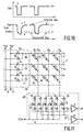
- the voltage V rst on the voltage supply line 19 is then pulsed negative as indicated by the line a in Figure 10 so turning on all the switching diodes 18 so that the voltage of each row conductor 5 falls as indicated by the solid line in Figure 10 to V unsel .
- the row conductors 5 are held (as indicated by the dashed line b in Figure 10) at the V unsel voltage by virtue of the row capacitance shown schematically in Figure 3 by the capacitors C r shown in dashed lines.
- the row capacitance could be simply that of the diodes and cross-overs on the row or may be an additional component provided at the periphery 7a of the second array 7.
- the required row ne is then selected by using the row and column drive circuitry 14 and 15 of the display 5 to cause the appropriate ones of the peripheral display elements 5' to transmit light to illuminate the peripheral photosensitive diode 11a associated with the required row.
- the photo current generated within the illuminated peripheral photosensitive diode 11a charges the row capacitance C r and raises the row voltage (as indicated by line in Figure 10) close to V se1 which selects the row.
- the voltage V se1 turns on the switching diodes 8b in each of the elements 8a in the selected row and a current flows through the element or pixel 8, charging the intrinsic capacitance of the photosensitive diode 8b to a known value.
- the amount of charge required is equal to the amount of charge generated by light incident on the photosensitive diode 8a.
- This charge is detected by the column read-out circuitry 100 in the following manner.
- the appropriate ones of the peripheral display elements 5' of the display 5 are controlled so as to transient light to illuminate the photosensitive diodes 11b as well as the photosensitive diode 11a of the selected row.
- the photosensitive diodes 11c are not illuminated at this time.
- the current flowing through each element 8 of the selected row flows down the associated column conductor 10 to the column capacitor C until the element or pixel 8 has been recharged to its starting point as indicated by the point x in Figure 10.
- the row is then de-selected by the application of the next voltage reset pulse V rst via the switching diodes 18 and the appropriate ones of the peripheral display elements 5' are controlled so that the photosensitive diodes 11a and diodes 11b are no longer illuminated.
- the appropriate ones of the peripheral display elements 5' of the display are then controlled so as to illuminate the photosensitive elements 11c one by one in sequence.
- the photosensitive diode 11c associated with a particular column conductor C is connected to a reference potential V ref and a current then flows from the charge-sensitive amplifier 21 to discharge the column capacitor C.
- the amplifier output voltage can then be sampled and subsequently processed using conventional means.
- Each row of the second array 7 is sequentially addressed in the same manner.
- the switching diodes 8b are not rendered conducting and so photogenerated charge is stored on the intrinsic capacitance of the photosensitive diodes 8a of the row.
- the period when this is happening is known as the integration period because effectively the charge stored at a photosensitive element 8a during this period represents an integral over the time the row is unselected of light incident on the photosensitive element 8a.
- the image sensor is being used, for example, to scan a document then generally only a single read of the second array 2 will be required so that in that case the integration time would be the time since the light source illuminating the document was turned on.
- the main display elements 5 of the display 3 may be used to illuminate a document placed over the image sensor array 7 so enabling the document to be in intimate contact with the second array 7.
- Figure 11 illustrates a modified version of the circuit layout shown in Figure 3. As will be evident from a comparison of Figures 3 and 11, the two differ in the construction of the row read-out circuitry 90' and the column read-out circuitry 100'.
- the switching diodes 18' are reversed in comparison to the switching diodes 18 shown in Figure 3 (that is the diodes 18' have their anodes connected to the supply line 19).
- the diodes 18' are also photosensitive, that is they have a similar structure to the diodes 11a.
- the reset pulse V rst can be applied to the row conductors 9 by illuminating the photosensitive diodes 18' appropriately.
- This arrangement has the advantage that the supply lines 17 and 18 need only supply constant (that is not pulsed) voltages and so these voltages may be provided by a suitable battery which can be mounted to the substrate 6.
- each pair of switching and photosensitive diode 18 and 11a by a single photosensitive diode (because the forward current of a diode is much higher than the photocurrent) and to enable resetting by applying a different voltage to the single voltage supply line.
- each column conductor 10 is associated with two photosensitive diodes 11b and 11'b, two photosensitive diodes 11c and 11'c and two column capacitors C and C'. All of the photosensitive diodes 11c and 11'c have their anodes coupled to the voltage reference line 22.
- the capacitors C are coupled via the connection line 20 to a charge sensitive amplifier 21 and the capacitors C1 coupled via a connection line 20' to a charge sensitive amplifier 21'.
- the photosensitive elements 11c are illuminated one by one in sequence by the appropriate ones of the peripheral display elements 5' so as to discharge the column capacitors C as discussed above with reference to Figure 3 to transfer the charge to the feedback capacitor of the charge sensitive amplifier.
- the second stage can be carried out in respect of the preceding row (the nth row) so reducing the overall time required to read-out all rows of the second array 7 by about one half.
- photosensitive diodes 11a,11b and 11c and switching diodes 18 have been shown in the Figures as being of similar structure to the photosensitive and switching diodes 8a and 8b, they may be of different geometry, for example of larger area, so as to provide the current handling capability required and they could if considered desirable be p-i-n as opposed to n-i-p diodes, for example.
- the modified row read-out circuitry 90' or the modified column read-out circuitry 100' shown in Figure 11 could be used in the example shown in Figure 3.
- the photosensitive elements 11a, 11b, 11c are sufficiently well spaced from adjacent similar photosensitive elements 11a, 11b, 11c that there is no significant cross-talk between the photosensitive elements 11a, 11b, 11c.
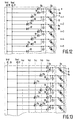
- the photosensitive elements 11a,11b and 11c may be staggered as shown in the schematic plan view in Figure 12 in a direction along the length of the associated row or column conductors 9 or 10 so as effectively to increase the spacing between adjacent photosensitive elements 11a, 11b, 11c.
- the photosensitive elements 11a are staggered so that in a direction along the row conductors 9, the n, n+3, etc. photosensitive elements 11a are aligned, that is so that each fourth element 11a is aligned.
- the spacing of the adjacent photosensitive elements 11a will of course depend upon the design rules of the device and any constraints on the overall size of the device. Any suitable staggered pattern may however be adopted.
- the photosensitive diodes 11b and 11c may be similarly staggered with, of course, the photosensitive diodes 11b and 11c associated with a respective column conductor being themselves spaced apart along the direction of the column conductor 10.
- the photosensitive elements 11a,11b,11c will be spaced by a similar distance from the associated display element 5' and so may have a similar spacing from one another. Normally the lateral spacing of the display elements 5' should be greater than the vertical separation between each display element 5' and the associated photosensitive element 11a,11b,11c.
- each row and each column conductor 9 and 10 is coupled via a single photosensitive element 11a, 11b, 11c to the associated voltage supply or connection line 17,20 and 22.
- each row conductor 9 is associated with one or more photosensitive elements 11a each aligned with a respective different column of periperal display elements 5' so that the row conductor 9 is only connected to the voltage supply line 17 when all of the associated photosensitive diodes 11a are rendered conducting.
- An example of such a pattern of photosensitive elements 11a is illustrated schematically in the diagram in Figure 13.
- the dashed lines numbered 14a to 14e represent columns of peripheral display elements 5' of the display 5.
- cross-talk between photosensitive diodes 11a associated with adjacent row conductors 9 does not present significant problems because, of course, each row conductor 9 will only be coupled to the voltage supply line V sel if all of the associated photosensitive elements 11a are rendered conducting.
- a similar structure could be used for the photosensitive diodes 11b,11c associated with the column conductors 10 where appropriate, for example where it is required to switch individual photosensitive diodes.
- EP-A-488455 describes the use of transistor, generally TFT buffers, to provide higher currents for charging the row capacitance and a similar idea could be used in the present device to increase the row select current.
- the image sensor transparency could be increased in a manner similar to that described, in our copending UK Patent Application No. 9209734.4 filed on 6th May 1992 which describes structures in which the number of row and column conductors in the second array 7 can be decreased by associating a number of photosensitive elements 8a with the same pair of row and column conductors 9 and 10 and providing some form of threshold adjustment means so that different voltage levels are required to assess different ones of the photosensitive elements 8a associated with the same pair of row and column conductors 9 and 10.
- the second array 7 could be any suitable type of array for example an array of electro-optically adjustable memory elements or photosensitive elements as discussed above or touch sensitive elements.
- the second array 7 could be another display controllable by the display 3 to allow superposition of images. Although this may present parallax problems it could be of advantage where an image is derived from a conventional analogue TV or video signal.
- the display array 4 and the second array 7 are both two dimensional active matrix arrays, this need not necessarily be the case and one or other of the arrays 4 and 7 may be one dimensional and/or a passive array.
Description
Claims (15)
- An electro-optic device comprising a first substrate (2) carrying an electro-optic display (3) having a first array (4) of display elements (5) and conductors (12, 13) for addressing display elements to enable the display to display an image, a second substrate (6) carrying a second array (7) of elements (8) addressable by conductors (9, 10) and photosensitive elements (11) associated with the conductors (9, 10) for supplying, when illuminated, signals along the conductors for accessing the elements (8) of the second array (7), the second substrate being provided opposite the first substrate (2) so that the photosensitive elements (11) are associated with selected ones (5') of the display elements (5) for enabling the selected display elements to illuminate the photosensitive elements allowing access of the elements of the second array to be controlled by the display.
- An electro-optic device according to Claim 1, wherein the electro-optic display (3) comprises a two-dimensional matrix array of display elements (5) arranged in row and columns with associated row and column conductors (12, 13) and the second array (7) is a two-dimensional array of elements (8) arranged in rows and columns with row and column conductors (9, 10) being associated with the elements of the second array so that supplying signals to a selected row conductor and a selected column conductor of the second array accesses an element of the second array and wherein the row and column conductors of the second array are associated with photosensitive elements (11) for supplying, when illuminated by selected ones of the display elements, signals along the row and column conductors for accessing the elements of the second array.
- An electro-optic device according to Claim 2, wherein each element (8) of the second array (7) is arranged to store charge and each row conductor (9) of the second array is coupled to a select voltage supply line (17) via at least one respective photosensitive element (11) so that in operation of the electro-optic device in order to read charge stored at the element within a row the at least one photosensitive element associated with the row is illuminated by the display to couple the select voltage to the row conductor.
- An electro-optic device according to Claim 3, wherein each row conductor (9) of the second array (7) is coupled to a reset voltage supply line (19) via a respective switching element (18) for enabling a reset voltage pulse to be applied to the row conductor to reset the associated elements.
- An electro-optic device according to Claim 3 or 4, wherein each column conductor (10) of the second array (7) is connected by at least one first photosensitive element (11) to one electrode of a respective column capacitor (C) having its other electrode coupled to a charge sensitive amplifier (21) and to at least one second photosensitive element (11) which is coupled to a voltage reference line (22) so that, in order to read charge from an element within a given column of the second array, first the associated at least one first photosensitive element is illuminated by the display for allowing the charge stored at an element in both the column and a row to which the select voltage is applied to be transferred via the column conductor and the at least one first photosensitive element to the capacitor and then the at least one second photosensitive element is illuminated to allow the charge stored at the column capacitor to be transferred to the charge sensitive amplifier.
- An electro-optic device according to Claim 3 or 4, wherein each column conductor (10) is coupled to one electrode of each of first and second column capacitors (C, C') by respective first photosensitive elements (11b, 11b') with each capacitor having its other electrode coupled to a respective charge sensitive amplifier (21, 21') and to a respective second photosensitive element (11c, 11c') coupled to a voltage reference line (22) so that, in order to read charge from an element within a given column of the second array, first one of the associated first photosensitive elements is illuminated by the display for allowing the charge stored at an element in both the column and a row to which the select voltage is applied to be transferred via the column conductor and the said one first photosensitive element to the associated one of the first and second capacitors and then the one of the second photosensitive elements is illuminated to allow the charge stored at the column capacitor to be transferred to the charge sensitive amplifier.
- An electro-optic device according to any of the preceding claims, wherein the photosensitive elements (11) are arranged at the periphery of the second array (7).
- An electro-optic device according to any one of the preceding claims, wherein each conductor (9, 10) of the second array is associated with at least one respective photosensitive element (11).
- An electro-optic device according to any one of the preceding claims, wherein each conductor (9, 10) of the second array (7) is associated with a number of photosensitive elements (11) arranged such that signals are only supplied along the conductor when all of the associated photosensitive elements are illuminated.
- An electro-optic device according to any one of the preceding claims, wherein the photosensitive elements (11) associated with adjacent conductors are staggered so that the spacing between the photosensitive elements associated with adjacent conductors is greater than the spacing between the adjacent conductors.
- An electro-optic device according to any one of the preceding claims, wherein the first and second arrays (4, 7) are of comparable size and the display elements (5) for illuminating the photosensitive elements are provided at the periphery of the first array.
- An electro-optic device according to any one of the preceding claims, wherein the display comprises a liquid crystal display.
- An electro-optic device according to any one of the preceding claims, wherein the second array (7) comprises an array of further photosensitive elements (8a).
- An electro-optic device according to any one of the preceding claims, wherein the second substrate (6) carrying the second array (7) is mounted to the first substrate (2) carrying the first array (4).
- An electro-optic device according to any one of the preceding claims, wherein the second substrate (6) carrying the second array is separable from the first substrate carrying the first array.
Applications Claiming Priority (2)
| Application Number | Priority Date | Filing Date | Title |
|---|---|---|---|
| GB939313841A GB9313841D0 (en) | 1993-07-05 | 1993-07-05 | An electro-optic device |
| GB9313841 | 1993-07-05 |
Publications (3)
| Publication Number | Publication Date |
|---|---|
| EP0633542A2 EP0633542A2 (en) | 1995-01-11 |
| EP0633542A3 EP0633542A3 (en) | 1998-06-10 |
| EP0633542B1 true EP0633542B1 (en) | 2001-10-17 |
Family
ID=10738301
Family Applications (1)
| Application Number | Title | Priority Date | Filing Date |
|---|---|---|---|
| EP94201882A Expired - Lifetime EP0633542B1 (en) | 1993-07-05 | 1994-06-30 | An electro-optic device |
Country Status (7)
| Country | Link |
|---|---|
| US (1) | US5483263A (en) |
| EP (1) | EP0633542B1 (en) |
| JP (1) | JPH0777704A (en) |
| KR (1) | KR100350001B1 (en) |
| DE (1) | DE69428638T2 (en) |
| GB (1) | GB9313841D0 (en) |
| TW (1) | TW250590B (en) |
Cited By (17)
| Publication number | Priority date | Publication date | Assignee | Title |
|---|---|---|---|---|
| US7542178B2 (en) | 2003-01-21 | 2009-06-02 | Hewlett-Packard Development Company, L.P. | Electronic device display and document scanner |
| US7773139B2 (en) | 2004-04-16 | 2010-08-10 | Apple Inc. | Image sensor with photosensitive thin film transistors |
| US7830461B2 (en) | 2002-05-23 | 2010-11-09 | Apple Inc. | Light sensitive display |
| US7872641B2 (en) | 2002-02-20 | 2011-01-18 | Apple Inc. | Light sensitive display |
| US8207946B2 (en) | 2003-02-20 | 2012-06-26 | Apple Inc. | Light sensitive display |
| US8441422B2 (en) | 2002-02-20 | 2013-05-14 | Apple Inc. | Light sensitive display with object detection calibration |
| US8638320B2 (en) | 2011-06-22 | 2014-01-28 | Apple Inc. | Stylus orientation detection |
| US8928635B2 (en) | 2011-06-22 | 2015-01-06 | Apple Inc. | Active stylus |
| US9176604B2 (en) | 2012-07-27 | 2015-11-03 | Apple Inc. | Stylus device |
| US9310923B2 (en) | 2010-12-03 | 2016-04-12 | Apple Inc. | Input device for touch sensitive devices |
| US9329703B2 (en) | 2011-06-22 | 2016-05-03 | Apple Inc. | Intelligent stylus |
| US9557845B2 (en) | 2012-07-27 | 2017-01-31 | Apple Inc. | Input device for and method of communication with capacitive devices through frequency variation |
| US9652090B2 (en) | 2012-07-27 | 2017-05-16 | Apple Inc. | Device for digital communication through capacitive coupling |
| US9939935B2 (en) | 2013-07-31 | 2018-04-10 | Apple Inc. | Scan engine for touch controller architecture |
| US10048775B2 (en) | 2013-03-14 | 2018-08-14 | Apple Inc. | Stylus detection and demodulation |
| US10061449B2 (en) | 2014-12-04 | 2018-08-28 | Apple Inc. | Coarse scan and targeted active mode scan for touch and stylus |
| US10474277B2 (en) | 2016-05-31 | 2019-11-12 | Apple Inc. | Position-based stylus communication |
Families Citing this family (45)
| Publication number | Priority date | Publication date | Assignee | Title |
|---|---|---|---|---|
| US5917464A (en) * | 1994-10-18 | 1999-06-29 | Xerox Corporation | Combination of 2-D detector array with display for image processing |
| SE504169C2 (en) * | 1995-02-13 | 1996-11-25 | Sten Eric Lindquist | Display combined with solar cell and battery |
| US5900767A (en) * | 1995-06-24 | 1999-05-04 | U.S. Philips Corporation | Electronic devices comprising an array |
| GB9512942D0 (en) * | 1995-06-24 | 1995-08-30 | Philips Electronics Uk Ltd | Electronic devices comprising an array |
| WO1997005597A1 (en) * | 1995-07-31 | 1997-02-13 | Litton Systems Canada Limited | Flat panel pixel array incorporating photoconductive switches |
| TW368671B (en) * | 1995-08-30 | 1999-09-01 | Tektronix Inc | Sputter-resistant, low-work-function, conductive coatings for cathode electrodes in DC plasma addressing structure |
| GB9524483D0 (en) * | 1995-11-30 | 1996-01-31 | Philips Electronics Nv | Light sensing array device and apparatus incorporating such |
| GB9614480D0 (en) * | 1995-12-01 | 1996-09-04 | Philips Electronics Nv | Multiplexer circuit |
| GB9524560D0 (en) * | 1995-12-01 | 1996-01-31 | Philips Electronics Nv | Multiplexer circuit |
| GB9603052D0 (en) * | 1996-02-14 | 1996-04-10 | Philips Electronics Nv | Image sensor |
| DE19720925B4 (en) * | 1996-05-29 | 2004-08-26 | Nawotec Gmbh | Device for entering information by means of an object approaching the device |
| GB9616265D0 (en) * | 1996-08-02 | 1996-09-11 | Philips Electronics Uk Ltd | Electron devices |
| TW403928B (en) * | 1996-08-16 | 2000-09-01 | Tektronix Inc | Sputter-resistant conductive coatings with enhanced emission of electrons for cathode electrodes in DC plasma addressing structure |
| JP2000193938A (en) * | 1998-12-28 | 2000-07-14 | Fujitsu Ltd | Driving method for liquid crystal display device |
| US7119759B2 (en) * | 1999-05-03 | 2006-10-10 | E Ink Corporation | Machine-readable displays |
| US7071907B1 (en) * | 1999-05-07 | 2006-07-04 | Candescent Technologies Corporation | Display with active contrast enhancement |
| GB0014962D0 (en) * | 2000-06-20 | 2000-08-09 | Koninkl Philips Electronics Nv | Matrix array display devices with light sensing elements and associated storage capacitors |
| GB2381643A (en) * | 2001-10-31 | 2003-05-07 | Cambridge Display Tech Ltd | Display drivers |
| US7023503B2 (en) * | 2002-02-20 | 2006-04-04 | Planar Systems, Inc. | Image sensor with photosensitive thin film transistors |
| AU2003216481A1 (en) * | 2002-03-01 | 2003-09-16 | Planar Systems, Inc. | Reflection resistant touch screens |
| JP2003332560A (en) * | 2002-05-13 | 2003-11-21 | Semiconductor Energy Lab Co Ltd | Semiconductor device and microprocessor |
| JP4227770B2 (en) * | 2002-07-10 | 2009-02-18 | シャープ株式会社 | Display device and image reading / display system including the same |
| JP4094386B2 (en) | 2002-09-02 | 2008-06-04 | 株式会社半導体エネルギー研究所 | Electronic circuit equipment |
| JP4373063B2 (en) | 2002-09-02 | 2009-11-25 | 株式会社半導体エネルギー研究所 | Electronic circuit equipment |
| US20060034492A1 (en) * | 2002-10-30 | 2006-02-16 | Roy Siegel | Hand recognition system |
| US7219241B2 (en) * | 2002-11-30 | 2007-05-15 | Intel Corporation | Method for managing virtual and actual performance states of logical processors in a multithreaded processor using system management mode |
| EP1579410A2 (en) * | 2002-12-30 | 2005-09-28 | Koninklijke Philips Electronics N.V. | Display device with capacitively connected pads |
| EP1584114A1 (en) * | 2003-01-17 | 2005-10-12 | Diode Solutions, Inc. | Display employing organic material |
| JP4574118B2 (en) * | 2003-02-12 | 2010-11-04 | 株式会社半導体エネルギー研究所 | Semiconductor device and manufacturing method thereof |
| US20080048995A1 (en) * | 2003-02-20 | 2008-02-28 | Planar Systems, Inc. | Light sensitive display |
| US8283679B2 (en) * | 2003-06-30 | 2012-10-09 | Semiconductor Energy Laboratory Co., Ltd. | Semiconductor device having light-emitting element and light-receiving element for transmitting among circuits formed over the plurality of substrates |
| US20050134749A1 (en) * | 2003-12-19 | 2005-06-23 | Adiel Abileah | Reflection resistant display |
| US8421715B2 (en) * | 2004-05-21 | 2013-04-16 | Semiconductor Energy Laboratory Co., Ltd. | Display device, driving method thereof and electronic appliance |
| US20070109239A1 (en) * | 2005-11-14 | 2007-05-17 | Den Boer Willem | Integrated light sensitive liquid crystal display |
| EP2749533B1 (en) * | 2006-04-04 | 2016-02-24 | Silicor Materials Inc. | Method for purifying silicon |
| US7525608B2 (en) * | 2006-08-14 | 2009-04-28 | Hannstar Display Corp. | Input display and fabrication method thereof |
| CN101622712B (en) * | 2006-11-07 | 2011-06-15 | 希百特股份有限公司 | Two-terminal switching devices and their methods of fabrication |
| US9741901B2 (en) | 2006-11-07 | 2017-08-22 | Cbrite Inc. | Two-terminal electronic devices and their methods of fabrication |
| US7898042B2 (en) * | 2006-11-07 | 2011-03-01 | Cbrite Inc. | Two-terminal switching devices and their methods of fabrication |
| US10824931B2 (en) * | 2012-08-30 | 2020-11-03 | Féinics Amatech Teoranta | Contactless smartcards with multiple coupling frames |
| WO2015143011A1 (en) * | 2014-03-19 | 2015-09-24 | Bidirectional Display Inc. | Image sensor panel and method for capturing graphical information using same |
| US9122349B1 (en) * | 2014-03-19 | 2015-09-01 | Bidirectional Display Inc. | Image sensor panel and method for capturing graphical information using same |
| CN106201149B (en) * | 2016-08-02 | 2019-07-09 | 厦门天马微电子有限公司 | Touch-control display panel and device |
| US10162462B2 (en) * | 2017-05-01 | 2018-12-25 | Synaptics Incorporated | Integrating capacitive sensing with an optical sensor |
| US11276346B2 (en) * | 2019-01-21 | 2022-03-15 | Novatek Microelectronics Corp. | Simplified sensing circuit and sample and hold circuit for improving uniformity in OLED driver |
Family Cites Families (9)
| Publication number | Priority date | Publication date | Assignee | Title |
|---|---|---|---|---|
| FR2469805A1 (en) * | 1979-11-09 | 1981-05-22 | Thomson Csf | MATRIX FOR DETECTION OF ELECTROMAGNETIC RADIATION AND RADIOLOGICAL IMAGE ENHANCER COMPRISING SUCH A MATRIX |
| JPS5685792A (en) * | 1979-12-14 | 1981-07-13 | Citizen Watch Co Ltd | Liquid crystal display unit |
| DE3511353A1 (en) * | 1985-03-28 | 1986-10-09 | Siemens Ag | Arrangement for inputting and processing characters and/or graphic patterns |
| FR2593343B1 (en) * | 1986-01-20 | 1988-03-25 | Thomson Csf | MATRIX OF PHOTOSENSITIVE ELEMENTS AND ITS MANUFACTURING METHOD, READING METHOD THEREOF, AND APPLICATION OF THIS MATRIX TO IMAGE TAKING |
| US4952031A (en) * | 1987-06-19 | 1990-08-28 | Victor Company Of Japan, Ltd. | Liquid crystal display device |
| FR2627924B1 (en) * | 1988-02-26 | 1990-06-22 | Thomson Csf | PHOTOSENSITIVE DEVICE AND IMAGE DETECTOR COMPRISING SUCH A DEVICE, PARTICULARLY A DOUBLE ENERGY IMAGE DETECTOR |
| FR2629932B1 (en) * | 1988-04-11 | 1991-01-25 | Thomson Csf | DOCUMENT READER |
| JPH02188818A (en) * | 1989-01-18 | 1990-07-24 | Hitachi Ltd | Handwritten input/output device and handwritten input system using the device |
| GB9026040D0 (en) * | 1990-11-30 | 1991-01-16 | Philips Electronic Associated | Addressable matrix device |
-
1993
- 1993-07-05 GB GB939313841A patent/GB9313841D0/en active Pending
-
1994
- 1994-04-08 TW TW083103086A patent/TW250590B/zh active
- 1994-05-11 US US08/241,317 patent/US5483263A/en not_active Expired - Fee Related
- 1994-06-30 DE DE69428638T patent/DE69428638T2/en not_active Expired - Fee Related
- 1994-06-30 KR KR1019940015381A patent/KR100350001B1/en not_active IP Right Cessation
- 1994-06-30 EP EP94201882A patent/EP0633542B1/en not_active Expired - Lifetime
- 1994-07-04 JP JP15219194A patent/JPH0777704A/en not_active Abandoned
Cited By (36)
| Publication number | Priority date | Publication date | Assignee | Title |
|---|---|---|---|---|
| US9134851B2 (en) | 2002-02-20 | 2015-09-15 | Apple Inc. | Light sensitive display |
| US11073926B2 (en) | 2002-02-20 | 2021-07-27 | Apple Inc. | Light sensitive display |
| US9411470B2 (en) | 2002-02-20 | 2016-08-09 | Apple Inc. | Light sensitive display with multiple data set object detection |
| US8570449B2 (en) | 2002-02-20 | 2013-10-29 | Apple Inc. | Light sensitive display with pressure sensor |
| US7872641B2 (en) | 2002-02-20 | 2011-01-18 | Apple Inc. | Light sensitive display |
| US8441422B2 (en) | 2002-02-20 | 2013-05-14 | Apple Inc. | Light sensitive display with object detection calibration |
| US7880819B2 (en) | 2002-05-23 | 2011-02-01 | Apple Inc. | Light sensitive display |
| US8044930B2 (en) | 2002-05-23 | 2011-10-25 | Apple Inc. | Light sensitive display |
| US7880733B2 (en) | 2002-05-23 | 2011-02-01 | Apple Inc. | Light sensitive display |
| US7852417B2 (en) | 2002-05-23 | 2010-12-14 | Apple Inc. | Light sensitive display |
| US7830461B2 (en) | 2002-05-23 | 2010-11-09 | Apple Inc. | Light sensitive display |
| US9354735B2 (en) | 2002-05-23 | 2016-05-31 | Apple Inc. | Light sensitive display |
| US7542178B2 (en) | 2003-01-21 | 2009-06-02 | Hewlett-Packard Development Company, L.P. | Electronic device display and document scanner |
| US8207946B2 (en) | 2003-02-20 | 2012-06-26 | Apple Inc. | Light sensitive display |
| US8289429B2 (en) | 2004-04-16 | 2012-10-16 | Apple Inc. | Image sensor with photosensitive thin film transistors and dark current compensation |
| US7773139B2 (en) | 2004-04-16 | 2010-08-10 | Apple Inc. | Image sensor with photosensitive thin film transistors |
| US9310923B2 (en) | 2010-12-03 | 2016-04-12 | Apple Inc. | Input device for touch sensitive devices |
| US9329703B2 (en) | 2011-06-22 | 2016-05-03 | Apple Inc. | Intelligent stylus |
| US8928635B2 (en) | 2011-06-22 | 2015-01-06 | Apple Inc. | Active stylus |
| US8638320B2 (en) | 2011-06-22 | 2014-01-28 | Apple Inc. | Stylus orientation detection |
| US9519361B2 (en) | 2011-06-22 | 2016-12-13 | Apple Inc. | Active stylus |
| US9921684B2 (en) | 2011-06-22 | 2018-03-20 | Apple Inc. | Intelligent stylus |
| US9557845B2 (en) | 2012-07-27 | 2017-01-31 | Apple Inc. | Input device for and method of communication with capacitive devices through frequency variation |
| US9582105B2 (en) | 2012-07-27 | 2017-02-28 | Apple Inc. | Input device for touch sensitive devices |
| US9652090B2 (en) | 2012-07-27 | 2017-05-16 | Apple Inc. | Device for digital communication through capacitive coupling |
| US9176604B2 (en) | 2012-07-27 | 2015-11-03 | Apple Inc. | Stylus device |
| US10048775B2 (en) | 2013-03-14 | 2018-08-14 | Apple Inc. | Stylus detection and demodulation |
| US9939935B2 (en) | 2013-07-31 | 2018-04-10 | Apple Inc. | Scan engine for touch controller architecture |
| US10067580B2 (en) | 2013-07-31 | 2018-09-04 | Apple Inc. | Active stylus for use with touch controller architecture |
| US10845901B2 (en) | 2013-07-31 | 2020-11-24 | Apple Inc. | Touch controller architecture |
| US11687192B2 (en) | 2013-07-31 | 2023-06-27 | Apple Inc. | Touch controller architecture |
| US10061450B2 (en) | 2014-12-04 | 2018-08-28 | Apple Inc. | Coarse scan and targeted active mode scan for touch |
| US10067618B2 (en) | 2014-12-04 | 2018-09-04 | Apple Inc. | Coarse scan and targeted active mode scan for touch |
| US10664113B2 (en) | 2014-12-04 | 2020-05-26 | Apple Inc. | Coarse scan and targeted active mode scan for touch and stylus |
| US10061449B2 (en) | 2014-12-04 | 2018-08-28 | Apple Inc. | Coarse scan and targeted active mode scan for touch and stylus |
| US10474277B2 (en) | 2016-05-31 | 2019-11-12 | Apple Inc. | Position-based stylus communication |
Also Published As
| Publication number | Publication date |
|---|---|
| TW250590B (en) | 1995-07-01 |
| KR100350001B1 (en) | 2002-12-26 |
| DE69428638T2 (en) | 2002-07-04 |
| US5483263A (en) | 1996-01-09 |
| EP0633542A3 (en) | 1998-06-10 |
| KR950003856A (en) | 1995-02-17 |
| EP0633542A2 (en) | 1995-01-11 |
| GB9313841D0 (en) | 1993-08-18 |
| DE69428638D1 (en) | 2001-11-22 |
| JPH0777704A (en) | 1995-03-20 |
Similar Documents
| Publication | Publication Date | Title |
|---|---|---|
| EP0633542B1 (en) | An electro-optic device | |
| EP0569090B1 (en) | Image sensor | |
| US5446564A (en) | Liquid crystal display device having photosensor at each pixel | |
| KR100470881B1 (en) | Electric circuit | |
| EP0509589B1 (en) | Optical touch input device | |
| JP2774424B2 (en) | Image input integrated display device | |
| EP0490683B1 (en) | Sensor arrays | |
| JP4590340B2 (en) | Liquid crystal display device and image sensing method using liquid crystal display device | |
| US7477445B2 (en) | Electrophoretic indication display | |
| US8508484B2 (en) | Liquid crystal display device | |
| KR101090254B1 (en) | Display device including sensing element | |
| KR20070027051A (en) | Touch sensible display device | |
| US5838290A (en) | Display device with photovoltaic converter | |
| US5426292A (en) | Image sensor having a two dimensional array of imaging elements with opposite polarity leakage currents | |
| US6753839B2 (en) | Electro-optical panel and electronic device | |
| JPH0797190B2 (en) | Storage device and liquid crystal display device | |
| WO2003071342A1 (en) | Lcd panel with image acquisition part and method of manufacturing same | |
| CN113946241A (en) | Display panel and display terminal | |
| JP2006509231A (en) | Active matrix display device | |
| US11842007B1 (en) | Display panel and display device | |
| CN114783389A (en) | Display panel | |
| WO1997005597A1 (en) | Flat panel pixel array incorporating photoconductive switches | |
| CN101086562A (en) | Two-dimensional display digital pixel and micro-sensing array combination |
Legal Events
| Date | Code | Title | Description |
|---|---|---|---|
| PUAI | Public reference made under article 153(3) epc to a published international application that has entered the european phase |
Free format text: ORIGINAL CODE: 0009012 |
|
| AK | Designated contracting states |
Kind code of ref document: A2 Designated state(s): DE FR GB NL |
|
| PUAL | Search report despatched |
Free format text: ORIGINAL CODE: 0009013 |
|
| AK | Designated contracting states |
Kind code of ref document: A3 Designated state(s): DE FR GB NL |
|
| 17P | Request for examination filed |
Effective date: 19981210 |
|
| 17Q | First examination report despatched |
Effective date: 19990308 |
|
| GRAG | Despatch of communication of intention to grant |
Free format text: ORIGINAL CODE: EPIDOS AGRA |
|
| GRAG | Despatch of communication of intention to grant |
Free format text: ORIGINAL CODE: EPIDOS AGRA |
|
| GRAH | Despatch of communication of intention to grant a patent |
Free format text: ORIGINAL CODE: EPIDOS IGRA |
|
| GRAH | Despatch of communication of intention to grant a patent |
Free format text: ORIGINAL CODE: EPIDOS IGRA |
|
| GRAA | (expected) grant |
Free format text: ORIGINAL CODE: 0009210 |
|
| AK | Designated contracting states |
Kind code of ref document: B1 Designated state(s): DE FR GB NL |
|
| PG25 | Lapsed in a contracting state [announced via postgrant information from national office to epo] |
Ref country code: NL Free format text: LAPSE BECAUSE OF FAILURE TO SUBMIT A TRANSLATION OF THE DESCRIPTION OR TO PAY THE FEE WITHIN THE PRESCRIBED TIME-LIMIT Effective date: 20011017 |
|
| REF | Corresponds to: |
Ref document number: 69428638 Country of ref document: DE Date of ref document: 20011122 |
|
| REG | Reference to a national code |
Ref country code: GB Ref legal event code: IF02 |
|
| ET | Fr: translation filed | ||
| NLV1 | Nl: lapsed or annulled due to failure to fulfill the requirements of art. 29p and 29m of the patents act | ||
| PLBE | No opposition filed within time limit |
Free format text: ORIGINAL CODE: 0009261 |
|
| STAA | Information on the status of an ep patent application or granted ep patent |
Free format text: STATUS: NO OPPOSITION FILED WITHIN TIME LIMIT |
|
| 26N | No opposition filed | ||
| PGFP | Annual fee paid to national office [announced via postgrant information from national office to epo] |
Ref country code: FR Payment date: 20030625 Year of fee payment: 10 |
|
| PGFP | Annual fee paid to national office [announced via postgrant information from national office to epo] |
Ref country code: GB Payment date: 20030627 Year of fee payment: 10 |
|
| PGFP | Annual fee paid to national office [announced via postgrant information from national office to epo] |
Ref country code: DE Payment date: 20030818 Year of fee payment: 10 |
|
| PG25 | Lapsed in a contracting state [announced via postgrant information from national office to epo] |
Ref country code: GB Free format text: LAPSE BECAUSE OF NON-PAYMENT OF DUE FEES Effective date: 20040630 |
|
| PG25 | Lapsed in a contracting state [announced via postgrant information from national office to epo] |
Ref country code: DE Free format text: LAPSE BECAUSE OF NON-PAYMENT OF DUE FEES Effective date: 20050101 |
|
| GBPC | Gb: european patent ceased through non-payment of renewal fee |
Effective date: 20040630 |
|
| PG25 | Lapsed in a contracting state [announced via postgrant information from national office to epo] |
Ref country code: FR Free format text: LAPSE BECAUSE OF NON-PAYMENT OF DUE FEES Effective date: 20050228 |
|
| REG | Reference to a national code |
Ref country code: FR Ref legal event code: ST |