EP0630002A1 - Method and apparatus for the simultaneous writing of data on an optical disk - Google Patents
Method and apparatus for the simultaneous writing of data on an optical disk Download PDFInfo
- Publication number
- EP0630002A1 EP0630002A1 EP94108778A EP94108778A EP0630002A1 EP 0630002 A1 EP0630002 A1 EP 0630002A1 EP 94108778 A EP94108778 A EP 94108778A EP 94108778 A EP94108778 A EP 94108778A EP 0630002 A1 EP0630002 A1 EP 0630002A1
- Authority
- EP
- European Patent Office
- Prior art keywords
- track
- writing
- light
- intensity
- data
- Prior art date
- Legal status (The legal status is an assumption and is not a legal conclusion. Google has not performed a legal analysis and makes no representation as to the accuracy of the status listed.)
- Ceased
Links
Images


Classifications
-
- G—PHYSICS
- G11—INFORMATION STORAGE
- G11B—INFORMATION STORAGE BASED ON RELATIVE MOVEMENT BETWEEN RECORD CARRIER AND TRANSDUCER
- G11B7/00—Recording or reproducing by optical means, e.g. recording using a thermal beam of optical radiation by modifying optical properties or the physical structure, reproducing using an optical beam at lower power by sensing optical properties; Record carriers therefor
- G11B7/12—Heads, e.g. forming of the optical beam spot or modulation of the optical beam
- G11B7/125—Optical beam sources therefor, e.g. laser control circuitry specially adapted for optical storage devices; Modulators, e.g. means for controlling the size or intensity of optical spots or optical traces
- G11B7/127—Lasers; Multiple laser arrays
-
- G—PHYSICS
- G11—INFORMATION STORAGE
- G11B—INFORMATION STORAGE BASED ON RELATIVE MOVEMENT BETWEEN RECORD CARRIER AND TRANSDUCER
- G11B7/00—Recording or reproducing by optical means, e.g. recording using a thermal beam of optical radiation by modifying optical properties or the physical structure, reproducing using an optical beam at lower power by sensing optical properties; Record carriers therefor
- G11B7/004—Recording, reproducing or erasing methods; Read, write or erase circuits therefor
- G11B7/0045—Recording
-
- G—PHYSICS
- G11—INFORMATION STORAGE
- G11B—INFORMATION STORAGE BASED ON RELATIVE MOVEMENT BETWEEN RECORD CARRIER AND TRANSDUCER
- G11B7/00—Recording or reproducing by optical means, e.g. recording using a thermal beam of optical radiation by modifying optical properties or the physical structure, reproducing using an optical beam at lower power by sensing optical properties; Record carriers therefor
- G11B7/08—Disposition or mounting of heads or light sources relatively to record carriers
- G11B7/09—Disposition or mounting of heads or light sources relatively to record carriers with provision for moving the light beam or focus plane for the purpose of maintaining alignment of the light beam relative to the record carrier during transducing operation, e.g. to compensate for surface irregularities of the latter or for track following
- G11B7/0901—Disposition or mounting of heads or light sources relatively to record carriers with provision for moving the light beam or focus plane for the purpose of maintaining alignment of the light beam relative to the record carrier during transducing operation, e.g. to compensate for surface irregularities of the latter or for track following for track following only
-
- G—PHYSICS
- G11—INFORMATION STORAGE
- G11B—INFORMATION STORAGE BASED ON RELATIVE MOVEMENT BETWEEN RECORD CARRIER AND TRANSDUCER
- G11B7/00—Recording or reproducing by optical means, e.g. recording using a thermal beam of optical radiation by modifying optical properties or the physical structure, reproducing using an optical beam at lower power by sensing optical properties; Record carriers therefor
- G11B7/12—Heads, e.g. forming of the optical beam spot or modulation of the optical beam
- G11B7/14—Heads, e.g. forming of the optical beam spot or modulation of the optical beam specially adapted to record on, or to reproduce from, more than one track simultaneously
Definitions
- the present invention relates to optical disks technology. More particularly, the invention relates to a method of simultaneous writing data on a plurality of tracks of an optical disk.
- an optical reading head for reading data tracks of optical disks, an apparatus enabling locking, tracking and reading data from many data tracks of an optical disk were described.
- This device comprises an optical apparatus for fast addressing of tracks on the disk, optical apparatus for imaging the tracks on a detector matrix comprising a plurality of detectors arranged in parallel lines, the said detector matrix being coupled to a plurality of shift registers, on which processing of the image is possible.
- the said device further comprises signal processing means to receive the data generated by the detector matrix, and to translate the said data into data contained in data spots located on the disk.
- the invention described in IL 101,570 is further directed to a method of accessing and reading data from an optical disk, which method comprises the steps of:
- a so-called "locking" operation is carried out, to determine the track center, and the coordinates of the track center initially found are used as the first value for the expected track center. Additionally, in another preferred embodiment, a number of track center values consecutively determined are considered, to permit statistical evaluation of drift and other system parameters.
- the ability to move the boundaries of the data strips electronically permits to compensate for drift in the disk movement. This compensation is critical for reading many tracks simultaneously, and the ability to compensate quickly for any such drift is an important feature, which permits to process large amounts of data at high rates.
- the head of the device as described therein can only read data in parallel, but cannot write data in parallel on many data tracks of the disk. Therefore, writing must be done by a conventional writing head, which writes data serially, one track at a time. This is a considerable disadvantage which limits the usefulness of the apparatus, particularly in cases where writing must be done rapidly.
- the method of writing data simultaneously on a plurality of tracks of an optical disk comprises providing an array of light sources, each light source being independently modulated, providing means to determine the position of each light source with respect to the center of a given track, and varying the intensity of each light source so as to generate a plurality of writing light beams, each generated by a plurality of adjacent light sources, each of the said light beams having the desired width, intensity and position on the written track.
- the light sources comprise a plurality of laser diodes.
- the invention provides for the generation of beams wherein the intensity of the light sources is varied so that their combined intensity exceeds the writing threshold value along the desired profile. Sub-threshold intensities are not considered to constitute a part of the beam profile, as they will not result in a writing on the disk.
- an apparatus for writing data simultaneously on a plurality of tracks of an optical disk comprising an array of light sources, means for independently modulate each of the said light sources, means for determining the position of each light source with respect to the center of a given track, and means for generating a plurality of writing light beams, each generated by a plurality of adjacent light sources, each of the said light beams having the desired width, intensity and position on the written track.
- the ability to redefine the position of each track center in a multi track area by modulating the light sources without mechanical adjustment enables the precise writing of many tracks simultaneously even when there are small drifts in the disk position and track locations.
- the invention is directed to a method of writing data on a track of an optical disk, comprising providing an array of light sources, each light source being independently modulated, providing means to determine the position of each light source with respect to the center of a given track, selecting a track on which data is to be written, and varying the intensity of each light source positioned within the selected track so as to generate a writing light beam by the combined effect of a plurality of adjacent light sources, the said light beam having the desired width, intensity and position on the written track.
- the invention in this aspect, also encompasses an apparatus for writing data on a track of an optical disk, comprising an array of light sources, means for independently modulate each of the said light sources, means for determining the position of each light source with respect to the center of a given track, means for selecting a track on which data is to be written, and means for varying the intensity of each light source positioned within the selected track so as to generate a writing light beam by the combined effect of a plurality of adjacent light sources, the said light beam having the desired width, intensity and position on the written track.
- Fig. 1 the preferred embodiment of the system for disk searching and reading is described.
- An optical disk 2 to be scanned by the system is placed in optical disk driver 4 which rotates the disk, reads the timing and tracking spots on one of the disk's tracks and sends timing signals to system controller 24.
- Above disk 2 there is an optional relay optics unit 6 that images the disk to intermediate image above it.
- the relay optics has a long optical path which creates enough space for optical elements such as the step and focus unit 8 or folding mirrors for multi disk configuration.
- the data is acquired by one or more reading heads 12, each one comprises of microscope 10, light source 16, detector matrix 14, focus sensor 18, and step and focus unit 8 as described in IL 101,570.
- the disk is illuminated by a light beam that is emitted from light unit 16, focused by microscope 10 and relayed by relay optics 6 to generate a uniform area of non-coherent illumination on disk 2.
- the required tracks of disk 2 are imaged by microscope 10 on detector matrix 14.
- the electrical signal that is generated by detector matrix 14 is processed by signal processing module 20. This module detects the presence and location of the sets of data spots. Data spots information is sent to storage module 22 and after structuring, the data is sent to a computer system (not shown).
- each image of data spot 52 of Fig. 2 lies over a square that contains nXm detectors.
- This nXm sampling of a data spot enables to localize a data spot on the right track when the disk has a small radial movement. It also enables to detect the presence of two succeeding data spots that are barely resolved. Because of the radial movement of the disk, the tracks can be shifted with large amplitude. In order not to loose the shifted tracks, the rows of detectors have to be long enough to "see" the shifted tracks as well. For global shift of amplitude w and for track width d, additional 2 ⁇ w/(d/m) detectors should be provided in the detector matrix 14. Alternatively, only small and fast shifts are compensated for electronically, and large slow shifts are mechanically compensated.
- Fig. 3 schematically illustrates image processing module 20.
- the module receives signals from detector matrix unit 14.
- the data from each shift register 66 of detector matrix 14 is fed to input memory buffers 70.
- Input memory buffers 70 are connected to a set of track processors (TP) 72 that detect the presence of image spots.
- TP track processors
- the input memory buffer can also seize as a multiplexing unit transferring only a section of the detector outputs into the processors.
- TP track processors
- the input memory buffer can also seize as a multiplexing unit transferring only a section of the detector outputs into the processors.
- the processing rate is reduced by the number of detectors "covered" by a spot. In the preferred embodiment of the invention a common reduction is by a factor of 9 from a pixel rate of 320 M/sec.
- Track detectors 72 align the spots on their right tracks. This alignment is done locally for small radial movement of the disk. More global alignment is done by system controller 24.
- TP 72 calculates the half-width distance between two of the nearest successive tracking spots 64 (in Fig. 2) of the sector header, and confirms this with the timing spot(s) 68 on the track center. If the disk is not formatted with tracking spots the locking is performed on the data spots, or on special pregroved track markers, if such exist.
- the sampling resolution is three pixels across each track.
- the maximum (or minimum) value across the track (over 4 pixels) is computed in sub-pixel resolution. The location of the maximum is recorded along the track. Any shift in the position of the maximum, relative to the current track center, is detected. The new track center is computed and the corresponding pixel nearest the center of the track is tagged as the central pixel of the track. For non sampled tracks, where the tracking points do not exist, the locking and tracking are performed on the track data or on special marks, if such exist.
- peak detection mechanism is quite similar to the edge detection mechanism, "peak location” meaning the location along a row of pixels across a track and between two track edges, where the maximum (or minimum) intensity value is located.
- the operator used for the peak detection is the First Difference operator 400, which is a one-dimensional operator consisting of two values: +1 and -1. Convolving the operator with pixels across the track direction, yields a convolved image comprising an array of positive, negative and possibly zero values. The zero-crossings between adjacent positive and negative values represents points of maxima and minima of the intensity levels. The gradient direction of the zero-crossing determines whether it is a minimum or a maximum. The exact position of each zero crossing is again computed in a sub-pixel accuracy, using interpolation. To reduce high-frequency noise it is possible to convolve the image with a one-dimensional low pass mask, across the tracks, before applying the First Difference operator.
- Fig. 10 illustrates the integration of the write illumination unit 500 into the read head apparatus.
- the illumination unit is controlled by the system controller 24 and emits the write beams through the beam splitter 128.
- Figs. 6a and 6b show the write illumination module 500 in detail.
- the light beam from writing light source 220 is focused by objective lens 118 to form an image on the disk of the laser diodes array 222. The sum of their light intensities is the desired writing spot of that track.
- Detector matrix 14 uses the reading beam to detect and locate the data tracks of the disk (as described earlier).
- the track-locking data is used by the system controller to operate the diode lasers of writing laser array 222.
- the resulting beam is shaped so that the writing spot is centered on the right track and its width is of the desired value.
- tracks can be written in parallel in such a way that each track has the writing spot of the desired width, intensity and position.
- writing laser diode 222 of writing light source 220 is comprised of a row of individually addressable laser diodes. Each laser diode is driven by one of the laser diode drivers 244 of writing source driver 240. The light beam from each laser diode is collimated by lens 224, reflected by beam splitter 120 toward objective lens 118. The lens focuses the collimated beam and generates an image of the diode laser array 222 on the disk.
- the focal length of lens 224 is chosen so that together with objective lens 118, a desired magnification (in fact, demagnification) of the laser diode array 222 is achieved.
- the number of the images of the laser diodes included in the data track of the disk is determined.
- the lens 224 is replaced by a lens array 300.
- multiple lenses are used to collimate the light, instead of a single large lens.
- This embodiment has the advantage of eliminating off axis aberration when there is a large number of lasers, i.e., a large field of view.
- the width and the intensity profile of the image of each laser diode of the writing laser diode array 222 is determined by the diffraction pattern of the image generated by the optical system. This pattern is determined by the numerical aperture of the objective lens and by the wavelength of the beam.
- the width of track 250 includes several images 252 of laser diode, each generating a diffraction pattern 254.
- the resulting intensity profile is a function of this overlapping and of the degree of coherence of the beam. At each point the intensity is the sum of the intensity of the overlapping diffraction patterns plus a term which is proportional to the degree of coherence.
- the intensity profile of the resultant beam is controlled. Because in the writing process light intensity must be above a threshold in order to affect the optical disk, the only important part of the intensity profile is that which is above the writing threshold 268.
- Fig. 8 is an example of the light intensity profile for five images of laser diodes that are symmetrically laid within the track.
- each image 252 of laser diode generates a diffraction pattern that has intensity profile 260.
- the resultant sum 262 of the intensities profiles is centered on the track 256.
- the relative weighing of the light intensity of each laser diode is changed so that the resulting sum of intensities has an intensity profile that is centered properly on the track.
- Fig. 9 is an example of such a shifted track.
- the relative intensity 264 of the diffraction pattern results in centered profile 266.
- the tracking and read operations are used for controlling the write position and for verifying the correctness of the written information.
- Fig. 11 illustrates the sequence of operations associate with the writing. First the read illumination is turned on. The tracking processor identifies with high accuracy the position offsets of the track centers. These position offsets are used as input to a look-up table out of which the weightings of the laser diodes is taken. In parallel with the writing, the read operation verifies the correctness of the written data. Continuous update of the weighting is done through the writing to correct for small position translation.
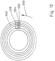
- Fig. 12 illustrates the spatial relations on the disk 560 between the read illumination 558 and the write illumination 552. As the disk rotates in the direction 550 the data spots 554 are being aligned and written using the tracking information. The written data is then verified with the read illumination 558. The distance between the read and the write illuminations is small enough so that no significant translation errors are created.
- the invention permits the writing of such a picture at a speed greater by one order of magnitude.
- Fig. 5 shows a digitized image function 440 of four pixels across a track: Pixel 442 has a value of 230; Pixel 444 has a value of 190; Pixel 446 has a value of 160; Pixel 448 has a value of 230.
- Pixel 452 represents the difference between pixels 442 and 444 and thus is located in space exactly between them. It has a value of 40. Similarly, Pixel 454 has a value of 30, Pixel 456 has a value of -70.
- the zero cross lies between pixels 454 and 456, viz., within Pixel 446.
- the track center is located at pixel 446, 0.3 pixel from its left boundary.
Abstract
A method of writing data simultaneously on a plurality of tracks of an optical disk, comprises providing an array of light sources (220), each light source being independently modulated, providing means to determine the position of each light source (220) with respect to the centre of a given track, and means (240) to vary the intensity of each light source so as to generate a plurality of writing light beams, each generated by a plurality of adjacent light sources (220), each of the said light beams having the desired width, intensity and position on the written track.
Description
- The present invention relates to optical disks technology. More particularly, the invention relates to a method of simultaneous writing data on a plurality of tracks of an optical disk.
- In a previous Israeli patent application No. 101,570 filed April 10, 1992 by the same applicants herein (corresponding to European Patent Application No. 93105995.0 and to U.S. Patent Application Ser. No. 08/043,254, filed April 6, 1993, the specification of which is incorporated herein by reference), an optical reading head for reading data tracks of optical disks, an apparatus enabling locking, tracking and reading data from many data tracks of an optical disk were described. This device comprises an optical apparatus for fast addressing of tracks on the disk, optical apparatus for imaging the tracks on a detector matrix comprising a plurality of detectors arranged in parallel lines, the said detector matrix being coupled to a plurality of shift registers, on which processing of the image is possible.
- The said device further comprises signal processing means to receive the data generated by the detector matrix, and to translate the said data into data contained in data spots located on the disk.
- The invention described in IL 101,570 is further directed to a method of accessing and reading data from an optical disk, which method comprises the steps of:
- 1) providing means for illuminating the required part of the disk and acquiring the optical image of a plurality of tracks;
- 2) providing a detector matrix comprising a plurality of detectors, each of the said detectors being capable of producing an output signal which is proportional to the intensity of the light detected by it;
- 3) causing an optical image corresponding to an illuminated area to fall on the said detector matrix;
- 4) transferring the output signal of the said detector matrix to image processing means;
- 5) determining position coordinates of the track center for each data track, by analyzing the output signal of the said detector matrix;
- 6) saving in memory means expected track center data, comprising position coordinates of the track center located by the said analysis of the output signal; and
- 7) if an actually detected track center is shifted with respect to the said expected track center, electronically moving the track center position.
- According to one embodiment of the abovementioned invention, at the beginning of the operation a so-called "locking" operation is carried out, to determine the track center, and the coordinates of the track center initially found are used as the first value for the expected track center. Additionally, in another preferred embodiment, a number of track center values consecutively determined are considered, to permit statistical evaluation of drift and other system parameters.
- As is apparent to a person skilled in the art, the ability to move the boundaries of the data strips electronically, by redefining the position of said boundaries and without the need for mechanical adjustment, permits to compensate for drift in the disk movement. This compensation is critical for reading many tracks simultaneously, and the ability to compensate quickly for any such drift is an important feature, which permits to process large amounts of data at high rates.
- The head of the device as described therein can only read data in parallel, but cannot write data in parallel on many data tracks of the disk. Therefore, writing must be done by a conventional writing head, which writes data serially, one track at a time. This is a considerable disadvantage which limits the usefulness of the apparatus, particularly in cases where writing must be done rapidly.
- It is an object of this invention to provide means by which it is possible also to write data simultaneously on plurality of tracks.
- The method of writing data simultaneously on a plurality of tracks of an optical disk, according to the invention, comprises providing an array of light sources, each light source being independently modulated, providing means to determine the position of each light source with respect to the center of a given track, and varying the intensity of each light source so as to generate a plurality of writing light beams, each generated by a plurality of adjacent light sources, each of the said light beams having the desired width, intensity and position on the written track. According to a preferred embodiment of the invention the light sources comprise a plurality of laser diodes.
- The invention provides for the generation of beams wherein the intensity of the light sources is varied so that their combined intensity exceeds the writing threshold value along the desired profile. Sub-threshold intensities are not considered to constitute a part of the beam profile, as they will not result in a writing on the disk.
- Also encompassed by the invention is an apparatus for writing data simultaneously on a plurality of tracks of an optical disk, comprising an array of light sources, means for independently modulate each of the said light sources, means for determining the position of each light source with respect to the center of a given track, and means for generating a plurality of writing light beams, each generated by a plurality of adjacent light sources, each of the said light beams having the desired width, intensity and position on the written track.
- As will be appreciated by the skilled person, the ability to redefine the position of each track center in a multi track area by modulating the light sources without mechanical adjustment enables the precise writing of many tracks simultaneously even when there are small drifts in the disk position and track locations.
- It should be noted that even when writing on a single track, some of the advantages of the invention are preserved, since no mechanical and precise servo mechanism is required. Thus, in another aspect, the invention is directed to a method of writing data on a track of an optical disk, comprising providing an array of light sources, each light source being independently modulated, providing means to determine the position of each light source with respect to the center of a given track, selecting a track on which data is to be written, and varying the intensity of each light source positioned within the selected track so as to generate a writing light beam by the combined effect of a plurality of adjacent light sources, the said light beam having the desired width, intensity and position on the written track.
- The invention, in this aspect, also encompasses an apparatus for writing data on a track of an optical disk, comprising an array of light sources, means for independently modulate each of the said light sources, means for determining the position of each light source with respect to the center of a given track, means for selecting a track on which data is to be written, and means for varying the intensity of each light source positioned within the selected track so as to generate a writing light beam by the combined effect of a plurality of adjacent light sources, the said light beam having the desired width, intensity and position on the written track.
- All the above and other characteristics and advantages of the invention will be better understood through the following description of illustrative and non-limitative preferred embodiments thereof.
-
- Fig. 1 schematically shows the main modules of the preferred embodiment of the invention of IL 101,570;
- Fig. 2 illustrates the reading of a number of tracks according to IL 101570;
- Fig. 3 is a schematic representation of one possible signal processing unit, according to IL 101570;
- Fig. 4 illustrates the peak detection operator according to IL 101570;
- Fig. 5 illustrates the peak detection process according to IL 101570;
- Fig. 6a illustrates an illumination device according to one embodiment of the invention;
- Fig. 6b illustrates an illumination device according to another embodiment of the invention;
- Fig. 7 shows spots as seen on a disk;
- Figs. 8 and 9 show light intensities obtained from light spots of Fig. 7;
- Fig. 10 schematically shows the main modules of one preferred embodiment of the invention;
- Fig. 11 illustrates the sequence of the writing operations;
- Fig. 12 shows the position of the read and write illuminations on the disk.
- In order to better appreciate the invention, some preferred embodiments of IL patent application No. 101,570 will be briefly described hereinafter.
- In Fig. 1, the preferred embodiment of the system for disk searching and reading is described. An
optical disk 2 to be scanned by the system is placed inoptical disk driver 4 which rotates the disk, reads the timing and tracking spots on one of the disk's tracks and sends timing signals tosystem controller 24. Abovedisk 2 there is an optional relay optics unit 6 that images the disk to intermediate image above it. The relay optics has a long optical path which creates enough space for optical elements such as the step andfocus unit 8 or folding mirrors for multi disk configuration. The data is acquired by one ormore reading heads 12, each one comprises ofmicroscope 10,light source 16,detector matrix 14,focus sensor 18, and step andfocus unit 8 as described in IL 101,570. The disk is illuminated by a light beam that is emitted fromlight unit 16, focused bymicroscope 10 and relayed by relay optics 6 to generate a uniform area of non-coherent illumination ondisk 2. The required tracks ofdisk 2 are imaged bymicroscope 10 ondetector matrix 14. The electrical signal that is generated bydetector matrix 14 is processed bysignal processing module 20. This module detects the presence and location of the sets of data spots. Data spots information is sent tostorage module 22 and after structuring, the data is sent to a computer system (not shown). - At any moment in time, each image of data spot 52 of Fig. 2 lies over a square that contains nXm detectors. This nXm sampling of a data spot enables to localize a data spot on the right track when the disk has a small radial movement. It also enables to detect the presence of two succeeding data spots that are barely resolved. Because of the radial movement of the disk, the tracks can be shifted with large amplitude. In order not to loose the shifted tracks, the rows of detectors have to be long enough to "see" the shifted tracks as well. For global shift of amplitude w and for track width d, additional 2·w/(d/m) detectors should be provided in the
detector matrix 14. Alternatively, only small and fast shifts are compensated for electronically, and large slow shifts are mechanically compensated. - Fig. 3 schematically illustrates
image processing module 20. The module receives signals fromdetector matrix unit 14. The data from eachshift register 66 ofdetector matrix 14 is fed to input memory buffers 70. Input memory buffers 70 are connected to a set of track processors (TP) 72 that detect the presence of image spots. The input memory buffer can also seize as a multiplexing unit transferring only a section of the detector outputs into the processors. By processing spots, the processing rate is reduced by the number of detectors "covered" by a spot. In the preferred embodiment of the invention a common reduction is by a factor of 9 from a pixel rate of 320 M/sec.Track detectors 72 align the spots on their right tracks. This alignment is done locally for small radial movement of the disk. More global alignment is done bysystem controller 24. - In the locking mode, the initial location of the center of the track is computed and set.
TP 72 calculates the half-width distance between two of the nearest successive tracking spots 64 (in Fig. 2) of the sector header, and confirms this with the timing spot(s) 68 on the track center. If the disk is not formatted with tracking spots the locking is performed on the data spots, or on special pregroved track markers, if such exist. - In the preferred embodiment of the invention, the sampling resolution is three pixels across each track. In the tracking mode, the maximum (or minimum) value across the track (over 4 pixels) is computed in sub-pixel resolution. The location of the maximum is recorded along the track. Any shift in the position of the maximum, relative to the current track center, is detected. The new track center is computed and the corresponding pixel nearest the center of the track is tagged as the central pixel of the track. For non sampled tracks, where the tracking points do not exist, the locking and tracking are performed on the track data or on special marks, if such exist.
- The mechanism for detecting the peaks in the tracking and locking process is further described below.
- The peak detection mechanism is quite similar to the edge detection mechanism, "peak location" meaning the location along a row of pixels across a track and between two track edges, where the maximum (or minimum) intensity value is located.
- Referring to Fig. 4, in the preferred embodiment of the invention, the operator used for the peak detection is the
First Difference operator 400, which is a one-dimensional operator consisting of two values: +1 and -1. Convolving the operator with pixels across the track direction, yields a convolved image comprising an array of positive, negative and possibly zero values. The zero-crossings between adjacent positive and negative values represents points of maxima and minima of the intensity levels. The gradient direction of the zero-crossing determines whether it is a minimum or a maximum. The exact position of each zero crossing is again computed in a sub-pixel accuracy, using interpolation. To reduce high-frequency noise it is possible to convolve the image with a one-dimensional low pass mask, across the tracks, before applying the First Difference operator. - Applying the first difference operator across track direction directly on the input signals has the disadvantage that neighboring pixels must be well calibrated. In order to alleviate this problem it is possible to apply first a first derivative type operator in the track direction, and then to search for the maximum (or minimum) value between the gradients in the cross track direction. To achieve higher stability in the results, the absolute value yielded by the first derivative operation are accumulated before comparison.
- In the following description, the invention will be illustrated with particular reference to illustrative and non-limitative preferred embodiments.
- The novel features of the invention are described with reference to Figs. 6 - 12.
- Fig. 10 illustrates the integration of the
write illumination unit 500 into the read head apparatus. The illumination unit is controlled by thesystem controller 24 and emits the write beams through thebeam splitter 128. Figs. 6a and 6b show thewrite illumination module 500 in detail. The light beam from writinglight source 220 is focused byobjective lens 118 to form an image on the disk of thelaser diodes array 222. The sum of their light intensities is the desired writing spot of that track.Detector matrix 14 uses the reading beam to detect and locate the data tracks of the disk (as described earlier). The track-locking data is used by the system controller to operate the diode lasers of writinglaser array 222. By proper weighing of the current of each laser diode, the resulting beam is shaped so that the writing spot is centered on the right track and its width is of the desired value. By using multiple laser diodes, tracks can be written in parallel in such a way that each track has the writing spot of the desired width, intensity and position. - Referring now to the write operation, as illustrated in Fig. 6a, writing
laser diode 222 of writinglight source 220 is comprised of a row of individually addressable laser diodes. Each laser diode is driven by one of thelaser diode drivers 244 of writingsource driver 240. The light beam from each laser diode is collimated bylens 224, reflected bybeam splitter 120 towardobjective lens 118. The lens focuses the collimated beam and generates an image of thediode laser array 222 on the disk. The focal length oflens 224 is chosen so that together withobjective lens 118, a desired magnification (in fact, demagnification) of thelaser diode array 222 is achieved. By this magnification, the number of the images of the laser diodes included in the data track of the disk is determined. In Fig. 6b thelens 224 is replaced by alens array 300. In this embodiment, multiple lenses are used to collimate the light, instead of a single large lens. This embodiment has the advantage of eliminating off axis aberration when there is a large number of lasers, i.e., a large field of view. - The width and the intensity profile of the image of each laser diode of the writing
laser diode array 222 is determined by the diffraction pattern of the image generated by the optical system. This pattern is determined by the numerical aperture of the objective lens and by the wavelength of the beam. - In Fig. 7, the relation between track, images of the laser diodes and their diffraction pattern is described. The width of
track 250 includesseveral images 252 of laser diode, each generating adiffraction pattern 254. For separation betweenimages 252 of the laser diode that is smaller than the width of thediffraction pattern 254 of each image, there will be partial overlapping between diffraction patterns of neighboring laser diodes. The resulting intensity profile is a function of this overlapping and of the degree of coherence of the beam. At each point the intensity is the sum of the intensity of the overlapping diffraction patterns plus a term which is proportional to the degree of coherence. By setting the intensity of each laser diode relative to its distance from the track center, the intensity profile of the resultant beam is controlled. Because in the writing process light intensity must be above a threshold in order to affect the optical disk, the only important part of the intensity profile is that which is above thewriting threshold 268. - Fig. 8 is an example of the light intensity profile for five images of laser diodes that are symmetrically laid within the track. Within the
track 256, eachimage 252 of laser diode generates a diffraction pattern that hasintensity profile 260. Theresultant sum 262 of the intensities profiles is centered on thetrack 256. When the track is shifted laterally so that images of the laser diodes are not centered symmetrically around the track center, the relative weighing of the light intensity of each laser diode is changed so that the resulting sum of intensities has an intensity profile that is centered properly on the track. Fig. 9 is an example of such a shifted track. Therelative intensity 264 of the diffraction pattern results incentered profile 266. By proper control of the light intensity of each laser diode, the width, intensity and center of the resultant profile at the threshold level can be controlled. - The tracking and read operations are used for controlling the write position and for verifying the correctness of the written information. Fig. 11 illustrates the sequence of operations associate with the writing. First the read illumination is turned on. The tracking processor identifies with high accuracy the position offsets of the track centers. These position offsets are used as input to a look-up table out of which the weightings of the laser diodes is taken. In parallel with the writing, the read operation verifies the correctness of the written data. Continuous update of the weighting is done through the writing to correct for small position translation.
- Fig. 12 illustrates the spatial relations on the
disk 560 between the readillumination 558 and the write illumination 552. As the disk rotates in thedirection 550 thedata spots 554 are being aligned and written using the tracking information. The written data is then verified with theread illumination 558. The distance between the read and the write illuminations is small enough so that no significant translation errors are created. - The following examples will further illustrate the invention, but are not intended to limit it in any way.
- This example illustrates the writing of data representing a picture from an optical disk, according to the invention. A Roentgen picture contains 2000 x 2000 pixels. Every pixel contains 12 bits. Each picture, therefore, contains 48 Mbit=6 Mbyte.
- Writing the picture to a conventional optical disk, having an addressing time of 70 msec, and a data writing rate of 1.25 Mbyte/sec, requires a time of:

- Writing the picture to a system according to the invention, having an addressing time of 15 msec, and a data writing rate of 20 Mbyte/sec, requires a time of:

- Therefore, the invention permits the writing of such a picture at a speed greater by one order of magnitude.
- Fig. 5 shows a
digitized image function 440 of four pixels across a track:
Pixel 442 has a value of 230;
Pixel 444 has a value of 190;
Pixel 446 has a value of 160;
Pixel 448 has a value of 230. - Applying the First Difference to this signal produces four new pixels with signed values and shifted in space by half a pixel:
Pixel 452 represents the difference betweenpixels Pixel 454 has a value of 30,Pixel 456 has a value of -70. - The zero cross lies between
pixels Pixel 446. The exact location is 30/(30+70) = 0.3 pixel. - Hence, the track center is located at
pixel 446, 0.3 pixel from its left boundary. - The above description of preferred embodiments has been given for the purpose of illustration, and should not be construed as a limitation of the invention in any way. Many changes can be effected in the method and apparatus of the invention. For instance, different light sources can be used, or different apparatus geometry can be devised, all without exceeding the scope of the invention.
Claims (13)
- A method of writing data simultaneously on a plurality of tracks of an optical disk, characterized in that it comprises an array of light sources (220), each light source (220) being independently modulated, means (72) to determine the position of each light source (220) with respect to the centre of a given track (256) and means (240) to vary the intensity of each light source (220) so as to generate a plurality of writing light beams, each generated by a plurality of adjacent light sources (220), each of the said light beams having the desired width, intensity and position on the written track (256).
- A method according to claim 1, wherein the light sources (220) comprise a plurality of laser diodes (222).
- A method according to claim 1, wherein the light beams are projected by multiple lenses (300).
- A method according to claim 1, wherein the intensity of the light sources (220) is varied so that their combined intensity (266) exceeds the threshold value (268) along the desired profile.
- A method according to claim 1, wherein at least one light beam is caused to illuminate each track (256) on which writing takes place.
- An apparatus for writing data simultaneously on a plurality of tracks of an optical disk, characterized in that it comprises an array of light sources (220), means (240) for independently modulate each of the said light sources (220), means (72) for determining the position of each light source (220) with respect to the centre of a given track (256) and means for generating a plurality of writing light beams, each generated by a plurality of adjacent light sources (220), each of the said light beams having the desired width, intensity and position on the written track (256).
- An apparatus according to claim 6, wherein the light sources (220) comprise a plurality of laser diodes (222).
- An apparatus according to claim 6, wherein the light beams are projected by multiple lenses (300).
- A method of writing data on a track of an optical disk, characterized in that it comprises an array of light sources (220), each light source (220) being independently modulated and means (72) to determine the position of each light source (220) with respect to the centre of a given track (256) selecting a track (256) on which data is to be written, and varying the intensity of each light source (220) positioned within the selected track (256) so as to generate a writing light beam by the combined effect of a plurality of adjacent light sources (220), the said light beam having the desired width, intensity and position on the written track (256).
- A method according to claim 9, wherein the light sources (220) comprise a plurality of laser diodes (222).
- An apparatus for writing data on a track of an optical disk, characterized in that it comprises an array of light sources (220), means (240) for independently modulate each of the said light sources (220), means (72) for determining the position of each light source (220) with respect to the centre of a given track (256), means for selecting a track on which data is to be written, and means (240) for varying the intensity of each light source positioned within the selected track (256) so as to generate a writing light beam by the combined effect of a plurality of adjacent light sources (220), the said light beam having the desired width, intensity and position on the written track.
- A method according to claim 1 or 9, wherein a reading head (12) capable of simultaneously reading the plurality of tracks (256) being written is positioned after the writing head to verify the correctness of the data written on the optical disk (2) by the writing head.
- Apparatus according to claim 6 or 11, characterized by further comprising a reading head (12) capable of simultaneously reading the plurality of tracks (256) being written, the said reading head (12) being positioned after the writing head in the direction of data writing.
Applications Claiming Priority (2)
| Application Number | Priority Date | Filing Date | Title |
|---|---|---|---|
| IL106009A IL106009A0 (en) | 1993-06-14 | 1993-06-14 | Method and apparatus for the simultaneous writing of data on an optical disk |
| IL10600993 | 1993-06-14 |
Publications (1)
| Publication Number | Publication Date |
|---|---|
| EP0630002A1 true EP0630002A1 (en) | 1994-12-21 |
Family
ID=11064947
Family Applications (1)
| Application Number | Title | Priority Date | Filing Date |
|---|---|---|---|
| EP94108778A Ceased EP0630002A1 (en) | 1993-06-14 | 1994-06-08 | Method and apparatus for the simultaneous writing of data on an optical disk |
Country Status (3)
| Country | Link |
|---|---|
| US (1) | US5592444A (en) |
| EP (1) | EP0630002A1 (en) |
| IL (1) | IL106009A0 (en) |
Cited By (7)
| Publication number | Priority date | Publication date | Assignee | Title |
|---|---|---|---|---|
| EP0810589A2 (en) * | 1996-05-27 | 1997-12-03 | Sony Corporation | Optical pickup device with a plurality of laser couplers |
| EP1125290A1 (en) * | 1998-09-28 | 2001-08-22 | T Squared G Incorporated | Multibyte random access mass storage/memory system |
| US6314071B1 (en) | 1998-02-20 | 2001-11-06 | Zen Research (Ireland), Ltd. | Method and apparatus for reading multiple tracks and writing at least one track of an optical disk |
| EP1245985A2 (en) * | 2001-03-30 | 2002-10-02 | Heidelberger Druckmaschinen Aktiengesellschaft | Image printing device with an optic of the Offner-type |
| US6888951B1 (en) | 1999-08-23 | 2005-05-03 | Nagaoka & Co., Ltd. | Methods and apparatus for analyzing operational and analyte data acquired from optical disc |
| US6902287B2 (en) | 2002-11-14 | 2005-06-07 | Safety Technology International, Inc. | Environmentally controlled appliance enclosure |
| US6985414B2 (en) | 2001-01-08 | 2006-01-10 | Dragsholm Wireless Holdings Llc | Method and apparatus for writing on an optical disk with beam spots aligned at an angle to data tracks |
Families Citing this family (19)
| Publication number | Priority date | Publication date | Assignee | Title |
|---|---|---|---|---|
| US5917788A (en) * | 1997-03-10 | 1999-06-29 | Seagate Technology, Inc. | Lens for optical data storage system |
| US6101155A (en) * | 1997-08-14 | 2000-08-08 | Seagate Technology, Inc. | Lens for optical data storage system |
| US6252715B1 (en) * | 1997-03-13 | 2001-06-26 | T. Squared G, Inc. | Beam pattern contractor and focus element, method and apparatus |
| US5870227A (en) * | 1997-03-13 | 1999-02-09 | T Squared G Systems, Inc. | Scanning head lens assembly |
| US6327241B1 (en) | 1997-04-08 | 2001-12-04 | Seagate Technology Llc | Optical data storage system with lens mount |
| US5930434A (en) * | 1997-05-15 | 1999-07-27 | Seagate Technology,. Inc. | Optical disc data storage system using optical waveguide |
| US5870362A (en) * | 1997-06-20 | 1999-02-09 | Seagate Technology, Inc. | Slider for optical disc data storage system |
| US5831797A (en) * | 1997-07-23 | 1998-11-03 | Seagate Technology, Inc. | Slider with mesa for optical disc data storage system |
| US6269066B1 (en) * | 1997-07-24 | 2001-07-31 | Richard L. Scully | Electronically translocatable optical stylet |
| US5917797A (en) * | 1997-08-15 | 1999-06-29 | Zen Research Nv | Multi-beam optical pickup assembly and methods using a compact two-dimensional arrangement of beams |
| US6445447B1 (en) | 1997-10-27 | 2002-09-03 | Seagate Technology Llc | Near field optical certifying head for disc asperity mapping |
| US6023378A (en) * | 1998-01-20 | 2000-02-08 | Seagate Technology, Inc. | Optical data storage system with improved head lens assembly |
| US6688743B1 (en) | 1998-02-17 | 2004-02-10 | Seagate Technology | Method and apparatus to determine fly height of a recording head |
| US6084846A (en) * | 1998-06-03 | 2000-07-04 | Seagate Technology, Inc. | Liquid immersion lens for optical data storage |
| US6208609B1 (en) | 1998-11-12 | 2001-03-27 | New Dimension Research & Instrument, Inc. | Optical system with interactive data capability |
| JP2003077146A (en) * | 2001-08-31 | 2003-03-14 | Sony Corp | Disk recorder and disk recording method |
| KR20080035010A (en) * | 2005-08-16 | 2008-04-22 | 코닌클리케 필립스 일렉트로닉스 엔.브이. | Optical system with a number of radiation sources |
| CN113744766A (en) * | 2020-05-29 | 2021-12-03 | 华为技术有限公司 | Data reading and writing device and data reading and writing method |
| CN116500306B (en) * | 2023-06-28 | 2023-10-27 | 鹏城实验室 | High-speed parallel writing and reading system and method |
Citations (2)
| Publication number | Priority date | Publication date | Assignee | Title |
|---|---|---|---|---|
| EP0092420A1 (en) * | 1982-04-19 | 1983-10-26 | Xerox Corporation | Information storage systems |
| US4428647A (en) * | 1982-11-04 | 1984-01-31 | Xerox Corporation | Multi-beam optical system using lens array |
Family Cites Families (34)
| Publication number | Priority date | Publication date | Assignee | Title |
|---|---|---|---|---|
| US3748015A (en) * | 1971-06-21 | 1973-07-24 | Perkin Elmer Corp | Unit power imaging catoptric anastigmat |
| BE789497A (en) * | 1971-09-29 | 1973-01-15 | Siemens Ag | DEVICE FOR CARRYING OUT THE SEQUENTIAL, INCONSISTENT AND REDUNDANT OPTICAL STORAGE OF INFORMATION |
| BE794494A (en) * | 1972-03-24 | 1974-08-05 | ||
| JPS54146613A (en) * | 1978-05-10 | 1979-11-16 | Hitachi Ltd | Optical head |
| US4536866A (en) * | 1978-11-30 | 1985-08-20 | Videonics Of Hawaii, Inc. | Information retrieval system and apparatus |
| EP0099651A3 (en) * | 1981-07-23 | 1984-03-21 | Comtech Research Unit Limited | Optical data storage |
| GB2120000B (en) * | 1982-04-28 | 1986-04-09 | Tdk Corp | Magnetic recording and reproduction |
| JPS59168942A (en) * | 1983-03-17 | 1984-09-22 | Matsushita Electric Ind Co Ltd | Optical recording and reproducing device |
| JPS59215033A (en) * | 1983-05-23 | 1984-12-04 | Hitachi Ltd | Optical disc recording and reproducing device |
| US4581529A (en) * | 1983-08-15 | 1986-04-08 | At&T Bell Laboratories | Read/write system for optical disc apparatus with fiber optics |
| JPH0777025B2 (en) * | 1985-10-16 | 1995-08-16 | 株式会社日立製作所 | Optical recording / reproducing device |
| JPS62259239A (en) * | 1986-05-06 | 1987-11-11 | Hitachi Ltd | Laminated optical disk device |
| JP2576542B2 (en) * | 1987-11-16 | 1997-01-29 | ソニー株式会社 | Optically recorded information reproducing device |
| JP2745529B2 (en) * | 1988-04-08 | 1998-04-28 | ソニー株式会社 | Optical recording medium playback device |
| US5065387A (en) * | 1988-04-07 | 1991-11-12 | Insite Peripherals, Inc. | Method and apparatus for generating tracking error signals by means of an optical servo system |
| JP2517104B2 (en) * | 1989-03-14 | 1996-07-24 | 富士通株式会社 | Beam track position control device and method for optical storage device |
| JPH02265028A (en) * | 1989-04-06 | 1990-10-29 | Mitsubishi Electric Corp | Optical recording and reproducing device |
| JPH02278533A (en) * | 1989-04-19 | 1990-11-14 | Eastman Kodatsuku Japan Kk | Optical head device for optical disk |
| US5181161A (en) * | 1989-04-21 | 1993-01-19 | Nec Corporation | Signal reproducing apparatus for optical recording and reproducing equipment with compensation of crosstalk from nearby tracks and method for the same |
| US5111445A (en) * | 1989-11-17 | 1992-05-05 | Sony Corporation | Holographic information storage system |
| US5247510A (en) * | 1990-06-29 | 1993-09-21 | Digital Equipment Corporation | Increasing storage density of optical data media by detecting a selected portion of a light spot image corresponding to a single domain |
| US5293569A (en) * | 1990-09-13 | 1994-03-08 | Canon Kabushiki Kaisha | Magneto-optical recording/reproducing apparatus including an optical head with an optical element having a plurality of prisms |
| US5081617A (en) * | 1990-09-24 | 1992-01-14 | Creo Products Inc. | Optical system for simultaneous reading of multiple data tracks |
| US5233583A (en) * | 1990-12-19 | 1993-08-03 | General Electric Company | Tracking and reading system for an optical medium and medium for use therewith |
| JPH04305821A (en) * | 1991-04-02 | 1992-10-28 | Sony Corp | Disk reproducing device |
| US5231627A (en) * | 1991-09-10 | 1993-07-27 | National Film Board Of Canada | Apparatus for reading optically encoded soundtracks |
| FR2683932B1 (en) * | 1991-11-19 | 1993-12-24 | Atg Sa | DEVICE FOR ACCESSING AND TRACKING TRACKS FOR OPTICAL DISCS. |
| US5365535A (en) * | 1992-01-13 | 1994-11-15 | Canon Kabushiki Kaisha | Semiconductor laser and beam splitting devices, and optical information recording/reproducing, optical communication, and optomagnetic recording/reproducing apparatuses using semiconductor laser and beam splitting devices |
| US5253245A (en) * | 1992-01-21 | 1993-10-12 | International Business Machines Corporation | Optical data storage tracking system |
| US5295125A (en) * | 1992-02-03 | 1994-03-15 | Hitachi, Ltd. | Optical head device for recording/reproduction for recording medium using plural light spots |
| IL101570A0 (en) * | 1992-04-10 | 1992-12-30 | Amir Alon | Method and apparatus for reading data |
| US5265085A (en) * | 1992-06-15 | 1993-11-23 | International Business Machines | Simultaneous MO and ROM optical disk signal detection |
| US5438563A (en) * | 1992-08-19 | 1995-08-01 | Olympus Optical Co., Ltd. | Optical information recording/reproducing device which simultaneously reproduces information from plural tracks and optical information recording/reproducing method |
| US5394385A (en) * | 1992-09-07 | 1995-02-28 | Olympus Optical Co., Ltd. | Optical information recording/reproducing apparatus for performing positioning of recording/reproducing spot by selection of pairs of photo detecting elements |
-
1993
- 1993-06-14 IL IL106009A patent/IL106009A0/en unknown
-
1994
- 1994-06-06 US US08/254,187 patent/US5592444A/en not_active Expired - Lifetime
- 1994-06-08 EP EP94108778A patent/EP0630002A1/en not_active Ceased
Patent Citations (2)
| Publication number | Priority date | Publication date | Assignee | Title |
|---|---|---|---|---|
| EP0092420A1 (en) * | 1982-04-19 | 1983-10-26 | Xerox Corporation | Information storage systems |
| US4428647A (en) * | 1982-11-04 | 1984-01-31 | Xerox Corporation | Multi-beam optical system using lens array |
Cited By (16)
| Publication number | Priority date | Publication date | Assignee | Title |
|---|---|---|---|---|
| KR100482228B1 (en) * | 1996-05-27 | 2005-07-18 | 소니 가부시끼 가이샤 | Optical pickup devices, compound optical devices and optical disc systems |
| EP0810589A3 (en) * | 1996-05-27 | 1998-07-01 | Sony Corporation | Optical pickup device with a plurality of laser couplers |
| US6091689A (en) * | 1996-05-27 | 2000-07-18 | Sony Corporation | Optical pickup device with a plurality of laser couplers |
| US6134208A (en) * | 1996-05-27 | 2000-10-17 | Sony Corporation | Optical pickup device with a plurality of laser couplers |
| EP0810589A2 (en) * | 1996-05-27 | 1997-12-03 | Sony Corporation | Optical pickup device with a plurality of laser couplers |
| US6314071B1 (en) | 1998-02-20 | 2001-11-06 | Zen Research (Ireland), Ltd. | Method and apparatus for reading multiple tracks and writing at least one track of an optical disk |
| EP1125290A1 (en) * | 1998-09-28 | 2001-08-22 | T Squared G Incorporated | Multibyte random access mass storage/memory system |
| EP1125290A4 (en) * | 1998-09-28 | 2007-01-17 | Squared G Inc T | Multibyte random access mass storage/memory system |
| US7664289B2 (en) | 1999-08-23 | 2010-02-16 | Vindur Technologies, Inc. | Methods and apparatus for analyzing operational and analyte data acquired from optical discs |
| US6888951B1 (en) | 1999-08-23 | 2005-05-03 | Nagaoka & Co., Ltd. | Methods and apparatus for analyzing operational and analyte data acquired from optical disc |
| US6985414B2 (en) | 2001-01-08 | 2006-01-10 | Dragsholm Wireless Holdings Llc | Method and apparatus for writing on an optical disk with beam spots aligned at an angle to data tracks |
| US7403465B2 (en) | 2001-01-08 | 2008-07-22 | Dragsholm Wireless Holdings Llc | Method and apparatus for writing on an optical disk with beam spots aligned at an angle to data tracks |
| US6661447B2 (en) | 2001-03-30 | 2003-12-09 | Heidelberger Druckmaschinen Ag | Image-recording device for a printing form having macrooptics of the offner type |
| EP1245985A3 (en) * | 2001-03-30 | 2002-10-09 | Heidelberger Druckmaschinen Aktiengesellschaft | Image printing device with an optic of the Offner-type |
| EP1245985A2 (en) * | 2001-03-30 | 2002-10-02 | Heidelberger Druckmaschinen Aktiengesellschaft | Image printing device with an optic of the Offner-type |
| US6902287B2 (en) | 2002-11-14 | 2005-06-07 | Safety Technology International, Inc. | Environmentally controlled appliance enclosure |
Also Published As
| Publication number | Publication date |
|---|---|
| IL106009A0 (en) | 1993-10-20 |
| US5592444A (en) | 1997-01-07 |
Similar Documents
| Publication | Publication Date | Title |
|---|---|---|
| US5592444A (en) | Method of writing data simultaneously on a plurality of tracks of an optical disk, and apparatus therefor | |
| EP0569718B1 (en) | Method and apparatus for reading data | |
| US4918415A (en) | Data reading and/or writing apparatus for use with an optical card | |
| US4507763A (en) | Optical information recording and/or reproducing apparatus and optical record medium for use in such apparatus | |
| KR980004526A (en) | Method and apparatus for holographic data storage system | |
| EP0245511A1 (en) | Optical card reader | |
| US5028102A (en) | Parallel optical information processing system | |
| RU2710004C1 (en) | Device and methods for predictive tracking of focus | |
| US5210730A (en) | Tracking error detecting apparatus for use in multibeam optical disk device | |
| US5239595A (en) | Optical method for identifying or recognizing a pattern to be identified | |
| CA2013074C (en) | Electro-optical ifs finder | |
| JPH05128574A (en) | Optical head | |
| JPH11218686A (en) | Optical image recording device and method utilising the device | |
| US6556307B1 (en) | Method and apparatus for inputting three-dimensional data | |
| US5199020A (en) | Optical head using an optical scanner | |
| WO2007054885A2 (en) | Method and system with focus control for scanning an information carrier | |
| US5179267A (en) | Data reading and/or writing apparatus of type using optical card | |
| KR0131566Y1 (en) | Optical pick-up skew control device | |
| KR102486540B1 (en) | Reagent analysis device and method of controlling the same | |
| US6750436B2 (en) | Focus error detection apparatus and method having dual focus error detection path | |
| US6946634B2 (en) | Optical pickup device | |
| JPS63117335A (en) | Reading method for optical card | |
| JP2828320B2 (en) | Electron beam length measurement method | |
| KR830000430B1 (en) | Reading device of optical radiation carrier | |
| US7911890B2 (en) | Optical disk unit |
Legal Events
| Date | Code | Title | Description |
|---|---|---|---|
| PUAI | Public reference made under article 153(3) epc to a published international application that has entered the european phase |
Free format text: ORIGINAL CODE: 0009012 |
|
| AK | Designated contracting states |
Kind code of ref document: A1 Designated state(s): BE DE DK ES FR GB IE IT NL SE |
|
| 17P | Request for examination filed |
Effective date: 19950612 |
|
| RAP1 | Party data changed (applicant data changed or rights of an application transferred) |
Owner name: ZEN RESEARCH N.V. |
|
| GRAG | Despatch of communication of intention to grant |
Free format text: ORIGINAL CODE: EPIDOS AGRA |
|
| 17Q | First examination report despatched |
Effective date: 19980429 |
|
| STAA | Information on the status of an ep patent application or granted ep patent |
Free format text: STATUS: THE APPLICATION HAS BEEN REFUSED |
|
| 18R | Application refused |
Effective date: 19981017 |