EP0629002A1 - Semiconductor device and ferroelectric capacitor - Google Patents
Semiconductor device and ferroelectric capacitor Download PDFInfo
- Publication number
- EP0629002A1 EP0629002A1 EP94108641A EP94108641A EP0629002A1 EP 0629002 A1 EP0629002 A1 EP 0629002A1 EP 94108641 A EP94108641 A EP 94108641A EP 94108641 A EP94108641 A EP 94108641A EP 0629002 A1 EP0629002 A1 EP 0629002A1
- Authority
- EP
- European Patent Office
- Prior art keywords
- layer
- substrate
- ferroelectric
- conductive metal
- region
- Prior art date
- Legal status (The legal status is an assumption and is not a legal conclusion. Google has not performed a legal analysis and makes no representation as to the accuracy of the status listed.)
- Granted
Links
- 239000004065 semiconductor Substances 0.000 title claims abstract description 30
- 239000003990 capacitor Substances 0.000 title claims abstract description 25
- WOCIAKWEIIZHES-UHFFFAOYSA-N ruthenium(iv) oxide Chemical compound O=[Ru]=O WOCIAKWEIIZHES-UHFFFAOYSA-N 0.000 claims abstract description 118
- 229910052751 metal Inorganic materials 0.000 claims abstract description 42
- 239000002184 metal Substances 0.000 claims abstract description 42
- 239000000758 substrate Substances 0.000 claims abstract description 42
- 229910044991 metal oxide Inorganic materials 0.000 claims abstract description 39
- 150000004706 metal oxides Chemical class 0.000 claims abstract description 39
- HTXDPTMKBJXEOW-UHFFFAOYSA-N dioxoiridium Chemical compound O=[Ir]=O HTXDPTMKBJXEOW-UHFFFAOYSA-N 0.000 claims abstract description 34
- 230000002829 reductive effect Effects 0.000 claims abstract description 26
- XUIMIQQOPSSXEZ-UHFFFAOYSA-N Silicon Chemical compound [Si] XUIMIQQOPSSXEZ-UHFFFAOYSA-N 0.000 claims abstract description 19
- 229910052710 silicon Inorganic materials 0.000 claims abstract description 19
- 239000010703 silicon Substances 0.000 claims abstract description 19
- KJTLSVCANCCWHF-UHFFFAOYSA-N Ruthenium Chemical compound [Ru] KJTLSVCANCCWHF-UHFFFAOYSA-N 0.000 claims abstract description 15
- 229910000489 osmium tetroxide Inorganic materials 0.000 claims abstract description 14
- 229910052702 rhenium Inorganic materials 0.000 claims abstract description 8
- 230000004888 barrier function Effects 0.000 claims abstract description 7
- WUAPFZMCVAUBPE-UHFFFAOYSA-N rhenium atom Chemical compound [Re] WUAPFZMCVAUBPE-UHFFFAOYSA-N 0.000 claims abstract description 7
- SYQBFIAQOQZEGI-UHFFFAOYSA-N osmium atom Chemical compound [Os] SYQBFIAQOQZEGI-UHFFFAOYSA-N 0.000 claims abstract description 6
- GKOZUEZYRPOHIO-UHFFFAOYSA-N iridium atom Chemical compound [Ir] GKOZUEZYRPOHIO-UHFFFAOYSA-N 0.000 claims abstract description 5
- 229910000457 iridium oxide Inorganic materials 0.000 claims abstract 2
- 229910000487 osmium oxide Inorganic materials 0.000 claims abstract 2
- 229910001925 ruthenium oxide Inorganic materials 0.000 claims abstract 2
- 239000010949 copper Substances 0.000 claims description 18
- 229910052707 ruthenium Inorganic materials 0.000 claims description 14
- 238000006243 chemical reaction Methods 0.000 claims description 12
- 230000003647 oxidation Effects 0.000 claims description 10
- 238000007254 oxidation reaction Methods 0.000 claims description 10
- 229910052802 copper Inorganic materials 0.000 claims description 7
- RYGMFSIKBFXOCR-UHFFFAOYSA-N Copper Chemical compound [Cu] RYGMFSIKBFXOCR-UHFFFAOYSA-N 0.000 claims description 6
- 230000009467 reduction Effects 0.000 claims description 6
- 230000002441 reversible effect Effects 0.000 claims description 5
- 238000000034 method Methods 0.000 abstract description 17
- WXBOMIKEWRRKBB-UHFFFAOYSA-N rhenium(iv) oxide Chemical compound O=[Re]=O WXBOMIKEWRRKBB-UHFFFAOYSA-N 0.000 abstract description 16
- 150000002739 metals Chemical class 0.000 abstract description 9
- 230000008569 process Effects 0.000 abstract description 5
- 239000010410 layer Substances 0.000 description 213
- 239000000463 material Substances 0.000 description 28
- GWEVSGVZZGPLCZ-UHFFFAOYSA-N Titan oxide Chemical compound O=[Ti]=O GWEVSGVZZGPLCZ-UHFFFAOYSA-N 0.000 description 23
- 239000001257 hydrogen Substances 0.000 description 16
- 229910052739 hydrogen Inorganic materials 0.000 description 16
- QVGXLLKOCUKJST-UHFFFAOYSA-N atomic oxygen Chemical compound [O] QVGXLLKOCUKJST-UHFFFAOYSA-N 0.000 description 15
- 229910052760 oxygen Inorganic materials 0.000 description 15
- 239000001301 oxygen Substances 0.000 description 15
- UFHFLCQGNIYNRP-UHFFFAOYSA-N Hydrogen Chemical compound [H][H] UFHFLCQGNIYNRP-UHFFFAOYSA-N 0.000 description 14
- 229910052581 Si3N4 Inorganic materials 0.000 description 14
- HQVNEWCFYHHQES-UHFFFAOYSA-N silicon nitride Chemical compound N12[Si]34N5[Si]62N3[Si]51N64 HQVNEWCFYHHQES-UHFFFAOYSA-N 0.000 description 13
- 239000000203 mixture Substances 0.000 description 12
- 230000001590 oxidative effect Effects 0.000 description 12
- 239000004408 titanium dioxide Substances 0.000 description 12
- 230000015572 biosynthetic process Effects 0.000 description 11
- 229910052451 lead zirconate titanate Inorganic materials 0.000 description 10
- 239000004020 conductor Substances 0.000 description 8
- 238000000151 deposition Methods 0.000 description 8
- BASFCYQUMIYNBI-UHFFFAOYSA-N platinum Chemical compound [Pt] BASFCYQUMIYNBI-UHFFFAOYSA-N 0.000 description 8
- 125000006850 spacer group Chemical group 0.000 description 8
- 239000012212 insulator Substances 0.000 description 7
- XKRFYHLGVUSROY-UHFFFAOYSA-N Argon Chemical compound [Ar] XKRFYHLGVUSROY-UHFFFAOYSA-N 0.000 description 6
- IJGRMHOSHXDMSA-UHFFFAOYSA-N Atomic nitrogen Chemical compound N#N IJGRMHOSHXDMSA-UHFFFAOYSA-N 0.000 description 6
- VYPSYNLAJGMNEJ-UHFFFAOYSA-N Silicium dioxide Chemical compound O=[Si]=O VYPSYNLAJGMNEJ-UHFFFAOYSA-N 0.000 description 6
- 239000003638 chemical reducing agent Substances 0.000 description 6
- 150000001875 compounds Chemical class 0.000 description 6
- BERDEBHAJNAUOM-UHFFFAOYSA-N copper(I) oxide Inorganic materials [Cu]O[Cu] BERDEBHAJNAUOM-UHFFFAOYSA-N 0.000 description 6
- KRFJLUBVMFXRPN-UHFFFAOYSA-N cuprous oxide Chemical compound [O-2].[Cu+].[Cu+] KRFJLUBVMFXRPN-UHFFFAOYSA-N 0.000 description 6
- 230000000873 masking effect Effects 0.000 description 6
- 230000036961 partial effect Effects 0.000 description 6
- 238000001020 plasma etching Methods 0.000 description 6
- YSZJKUDBYALHQE-UHFFFAOYSA-N rhenium trioxide Chemical compound O=[Re](=O)=O YSZJKUDBYALHQE-UHFFFAOYSA-N 0.000 description 6
- TXEYQDLBPFQVAA-UHFFFAOYSA-N tetrafluoromethane Chemical compound FC(F)(F)F TXEYQDLBPFQVAA-UHFFFAOYSA-N 0.000 description 6
- 230000008021 deposition Effects 0.000 description 5
- 238000000992 sputter etching Methods 0.000 description 5
- KRHYYFGTRYWZRS-UHFFFAOYSA-N Fluorane Chemical compound F KRHYYFGTRYWZRS-UHFFFAOYSA-N 0.000 description 4
- MHAJPDPJQMAIIY-UHFFFAOYSA-N Hydrogen peroxide Chemical compound OO MHAJPDPJQMAIIY-UHFFFAOYSA-N 0.000 description 4
- RTAQQCXQSZGOHL-UHFFFAOYSA-N Titanium Chemical compound [Ti] RTAQQCXQSZGOHL-UHFFFAOYSA-N 0.000 description 4
- NRTOMJZYCJJWKI-UHFFFAOYSA-N Titanium nitride Chemical compound [Ti]#N NRTOMJZYCJJWKI-UHFFFAOYSA-N 0.000 description 4
- 229910052741 iridium Inorganic materials 0.000 description 4
- 229910052762 osmium Inorganic materials 0.000 description 4
- 238000000059 patterning Methods 0.000 description 4
- 229910052697 platinum Inorganic materials 0.000 description 4
- 239000011241 protective layer Substances 0.000 description 4
- VZGDMQKNWNREIO-UHFFFAOYSA-N tetrachloromethane Chemical compound ClC(Cl)(Cl)Cl VZGDMQKNWNREIO-UHFFFAOYSA-N 0.000 description 4
- 229910052719 titanium Inorganic materials 0.000 description 4
- 239000010936 titanium Substances 0.000 description 4
- 239000005749 Copper compound Substances 0.000 description 3
- YCKRFDGAMUMZLT-UHFFFAOYSA-N Fluorine atom Chemical compound [F] YCKRFDGAMUMZLT-UHFFFAOYSA-N 0.000 description 3
- ZOKXTWBITQBERF-UHFFFAOYSA-N Molybdenum Chemical compound [Mo] ZOKXTWBITQBERF-UHFFFAOYSA-N 0.000 description 3
- QCWXUUIWCKQGHC-UHFFFAOYSA-N Zirconium Chemical compound [Zr] QCWXUUIWCKQGHC-UHFFFAOYSA-N 0.000 description 3
- 229910052786 argon Inorganic materials 0.000 description 3
- 230000015556 catabolic process Effects 0.000 description 3
- 150000001880 copper compounds Chemical class 0.000 description 3
- 238000006731 degradation reaction Methods 0.000 description 3
- 238000005530 etching Methods 0.000 description 3
- 229910052731 fluorine Inorganic materials 0.000 description 3
- 239000011737 fluorine Substances 0.000 description 3
- 239000001307 helium Substances 0.000 description 3
- 229910052734 helium Inorganic materials 0.000 description 3
- SWQJXJOGLNCZEY-UHFFFAOYSA-N helium atom Chemical compound [He] SWQJXJOGLNCZEY-UHFFFAOYSA-N 0.000 description 3
- HTUMBQDCCIXGCV-UHFFFAOYSA-N lead oxide Chemical compound [O-2].[Pb+2] HTUMBQDCCIXGCV-UHFFFAOYSA-N 0.000 description 3
- 229910052750 molybdenum Inorganic materials 0.000 description 3
- 239000011733 molybdenum Substances 0.000 description 3
- 229910052757 nitrogen Inorganic materials 0.000 description 3
- 238000012545 processing Methods 0.000 description 3
- 235000012239 silicon dioxide Nutrition 0.000 description 3
- 239000000377 silicon dioxide Substances 0.000 description 3
- 238000004544 sputter deposition Methods 0.000 description 3
- 238000001039 wet etching Methods 0.000 description 3
- 229910052726 zirconium Inorganic materials 0.000 description 3
- KZBUYRJDOAKODT-UHFFFAOYSA-N Chlorine Chemical compound ClCl KZBUYRJDOAKODT-UHFFFAOYSA-N 0.000 description 2
- FYYHWMGAXLPEAU-UHFFFAOYSA-N Magnesium Chemical compound [Mg] FYYHWMGAXLPEAU-UHFFFAOYSA-N 0.000 description 2
- GRYLNZFGIOXLOG-UHFFFAOYSA-N Nitric acid Chemical compound O[N+]([O-])=O GRYLNZFGIOXLOG-UHFFFAOYSA-N 0.000 description 2
- KDLHZDBZIXYQEI-UHFFFAOYSA-N Palladium Chemical compound [Pd] KDLHZDBZIXYQEI-UHFFFAOYSA-N 0.000 description 2
- -1 RuO2 Chemical class 0.000 description 2
- 230000008859 change Effects 0.000 description 2
- 238000005229 chemical vapour deposition Methods 0.000 description 2
- 238000007796 conventional method Methods 0.000 description 2
- 238000001312 dry etching Methods 0.000 description 2
- 150000002431 hydrogen Chemical class 0.000 description 2
- 239000011261 inert gas Substances 0.000 description 2
- 238000009413 insulation Methods 0.000 description 2
- 229910000765 intermetallic Inorganic materials 0.000 description 2
- 229910052749 magnesium Inorganic materials 0.000 description 2
- 239000011777 magnesium Substances 0.000 description 2
- KELHQGOVULCJSG-UHFFFAOYSA-N n,n-dimethyl-1-(5-methylfuran-2-yl)ethane-1,2-diamine Chemical compound CN(C)C(CN)C1=CC=C(C)O1 KELHQGOVULCJSG-UHFFFAOYSA-N 0.000 description 2
- 229910017604 nitric acid Inorganic materials 0.000 description 2
- 238000002161 passivation Methods 0.000 description 2
- 229910052715 tantalum Inorganic materials 0.000 description 2
- GUVRBAGPIYLISA-UHFFFAOYSA-N tantalum atom Chemical compound [Ta] GUVRBAGPIYLISA-UHFFFAOYSA-N 0.000 description 2
- WFKWXMTUELFFGS-UHFFFAOYSA-N tungsten Chemical compound [W] WFKWXMTUELFFGS-UHFFFAOYSA-N 0.000 description 2
- 229910052721 tungsten Inorganic materials 0.000 description 2
- 239000010937 tungsten Substances 0.000 description 2
- ZAMOUSCENKQFHK-UHFFFAOYSA-N Chlorine atom Chemical compound [Cl] ZAMOUSCENKQFHK-UHFFFAOYSA-N 0.000 description 1
- 229910003087 TiOx Inorganic materials 0.000 description 1
- 238000000137 annealing Methods 0.000 description 1
- 239000000460 chlorine Substances 0.000 description 1
- 229910052801 chlorine Inorganic materials 0.000 description 1
- 230000008878 coupling Effects 0.000 description 1
- 238000010168 coupling process Methods 0.000 description 1
- 238000005859 coupling reaction Methods 0.000 description 1
- 239000007789 gas Substances 0.000 description 1
- 239000002784 hot electron Substances 0.000 description 1
- 150000002500 ions Chemical class 0.000 description 1
- 238000002955 isolation Methods 0.000 description 1
- HFGPZNIAWCZYJU-UHFFFAOYSA-N lead zirconate titanate Chemical compound [O-2].[O-2].[O-2].[O-2].[O-2].[Ti+4].[Zr+4].[Pb+2] HFGPZNIAWCZYJU-UHFFFAOYSA-N 0.000 description 1
- 230000000670 limiting effect Effects 0.000 description 1
- 230000014759 maintenance of location Effects 0.000 description 1
- 230000015654 memory Effects 0.000 description 1
- 239000007769 metal material Substances 0.000 description 1
- 230000005012 migration Effects 0.000 description 1
- 238000013508 migration Methods 0.000 description 1
- 238000012986 modification Methods 0.000 description 1
- 230000004048 modification Effects 0.000 description 1
- 150000004767 nitrides Chemical class 0.000 description 1
- YEXPOXQUZXUXJW-UHFFFAOYSA-N oxolead Chemical compound [Pb]=O YEXPOXQUZXUXJW-UHFFFAOYSA-N 0.000 description 1
- 229910052763 palladium Inorganic materials 0.000 description 1
- 238000000623 plasma-assisted chemical vapour deposition Methods 0.000 description 1
- 238000005498 polishing Methods 0.000 description 1
- 229910021420 polycrystalline silicon Inorganic materials 0.000 description 1
- 229920005591 polysilicon Polymers 0.000 description 1
- 230000001681 protective effect Effects 0.000 description 1
- 238000004528 spin coating Methods 0.000 description 1
- HLLICFJUWSZHRJ-UHFFFAOYSA-N tioxidazole Chemical compound CCCOC1=CC=C2N=C(NC(=O)OC)SC2=C1 HLLICFJUWSZHRJ-UHFFFAOYSA-N 0.000 description 1
- OGIDPMRJRNCKJF-UHFFFAOYSA-N titanium oxide Inorganic materials [Ti]=O OGIDPMRJRNCKJF-UHFFFAOYSA-N 0.000 description 1
- MAKDTFFYCIMFQP-UHFFFAOYSA-N titanium tungsten Chemical compound [Ti].[W] MAKDTFFYCIMFQP-UHFFFAOYSA-N 0.000 description 1
- 230000009466 transformation Effects 0.000 description 1
Images


Classifications
-
- H—ELECTRICITY
- H01—ELECTRIC ELEMENTS
- H01L—SEMICONDUCTOR DEVICES NOT COVERED BY CLASS H10
- H01L21/00—Processes or apparatus adapted for the manufacture or treatment of semiconductor or solid state devices or of parts thereof
- H01L21/02—Manufacture or treatment of semiconductor devices or of parts thereof
- H01L21/04—Manufacture or treatment of semiconductor devices or of parts thereof the devices having at least one potential-jump barrier or surface barrier, e.g. PN junction, depletion layer or carrier concentration layer
- H01L21/18—Manufacture or treatment of semiconductor devices or of parts thereof the devices having at least one potential-jump barrier or surface barrier, e.g. PN junction, depletion layer or carrier concentration layer the devices having semiconductor bodies comprising elements of Group IV of the Periodic System or AIIIBV compounds with or without impurities, e.g. doping materials
- H01L21/28—Manufacture of electrodes on semiconductor bodies using processes or apparatus not provided for in groups H01L21/20 - H01L21/268
-
- H—ELECTRICITY
- H01—ELECTRIC ELEMENTS
- H01L—SEMICONDUCTOR DEVICES NOT COVERED BY CLASS H10
- H01L23/00—Details of semiconductor or other solid state devices
- H01L23/52—Arrangements for conducting electric current within the device in operation from one component to another, i.e. interconnections, e.g. wires, lead frames
- H01L23/522—Arrangements for conducting electric current within the device in operation from one component to another, i.e. interconnections, e.g. wires, lead frames including external interconnections consisting of a multilayer structure of conductive and insulating layers inseparably formed on the semiconductor body
- H01L23/5226—Via connections in a multilevel interconnection structure
-
- H—ELECTRICITY
- H10—SEMICONDUCTOR DEVICES; ELECTRIC SOLID-STATE DEVICES NOT OTHERWISE PROVIDED FOR
- H10B—ELECTRONIC MEMORY DEVICES
- H10B53/00—Ferroelectric RAM [FeRAM] devices comprising ferroelectric memory capacitors
-
- H—ELECTRICITY
- H01—ELECTRIC ELEMENTS
- H01L—SEMICONDUCTOR DEVICES NOT COVERED BY CLASS H10
- H01L21/00—Processes or apparatus adapted for the manufacture or treatment of semiconductor or solid state devices or of parts thereof
- H01L21/70—Manufacture or treatment of devices consisting of a plurality of solid state components formed in or on a common substrate or of parts thereof; Manufacture of integrated circuit devices or of parts thereof
- H01L21/71—Manufacture of specific parts of devices defined in group H01L21/70
- H01L21/768—Applying interconnections to be used for carrying current between separate components within a device comprising conductors and dielectrics
- H01L21/76838—Applying interconnections to be used for carrying current between separate components within a device comprising conductors and dielectrics characterised by the formation and the after-treatment of the conductors
- H01L21/76841—Barrier, adhesion or liner layers
- H01L21/76843—Barrier, adhesion or liner layers formed in openings in a dielectric
- H01L21/76849—Barrier, adhesion or liner layers formed in openings in a dielectric the layer being positioned on top of the main fill metal
-
- H—ELECTRICITY
- H01—ELECTRIC ELEMENTS
- H01L—SEMICONDUCTOR DEVICES NOT COVERED BY CLASS H10
- H01L23/00—Details of semiconductor or other solid state devices
- H01L23/52—Arrangements for conducting electric current within the device in operation from one component to another, i.e. interconnections, e.g. wires, lead frames
- H01L23/522—Arrangements for conducting electric current within the device in operation from one component to another, i.e. interconnections, e.g. wires, lead frames including external interconnections consisting of a multilayer structure of conductive and insulating layers inseparably formed on the semiconductor body
- H01L23/532—Arrangements for conducting electric current within the device in operation from one component to another, i.e. interconnections, e.g. wires, lead frames including external interconnections consisting of a multilayer structure of conductive and insulating layers inseparably formed on the semiconductor body characterised by the materials
- H01L23/53204—Conductive materials
- H01L23/53209—Conductive materials based on metals, e.g. alloys, metal silicides
- H01L23/53228—Conductive materials based on metals, e.g. alloys, metal silicides the principal metal being copper
- H01L23/53238—Additional layers associated with copper layers, e.g. adhesion, barrier, cladding layers
-
- H—ELECTRICITY
- H01—ELECTRIC ELEMENTS
- H01L—SEMICONDUCTOR DEVICES NOT COVERED BY CLASS H10
- H01L23/00—Details of semiconductor or other solid state devices
- H01L23/52—Arrangements for conducting electric current within the device in operation from one component to another, i.e. interconnections, e.g. wires, lead frames
- H01L23/522—Arrangements for conducting electric current within the device in operation from one component to another, i.e. interconnections, e.g. wires, lead frames including external interconnections consisting of a multilayer structure of conductive and insulating layers inseparably formed on the semiconductor body
- H01L23/532—Arrangements for conducting electric current within the device in operation from one component to another, i.e. interconnections, e.g. wires, lead frames including external interconnections consisting of a multilayer structure of conductive and insulating layers inseparably formed on the semiconductor body characterised by the materials
- H01L23/5329—Insulating materials
-
- H—ELECTRICITY
- H01—ELECTRIC ELEMENTS
- H01L—SEMICONDUCTOR DEVICES NOT COVERED BY CLASS H10
- H01L28/00—Passive two-terminal components without a potential-jump or surface barrier for integrated circuits; Details thereof; Multistep manufacturing processes therefor
- H01L28/40—Capacitors
-
- H—ELECTRICITY
- H01—ELECTRIC ELEMENTS
- H01L—SEMICONDUCTOR DEVICES NOT COVERED BY CLASS H10
- H01L28/00—Passive two-terminal components without a potential-jump or surface barrier for integrated circuits; Details thereof; Multistep manufacturing processes therefor
- H01L28/40—Capacitors
- H01L28/60—Electrodes
-
- H—ELECTRICITY
- H01—ELECTRIC ELEMENTS
- H01L—SEMICONDUCTOR DEVICES NOT COVERED BY CLASS H10
- H01L29/00—Semiconductor devices adapted for rectifying, amplifying, oscillating or switching, or capacitors or resistors with at least one potential-jump barrier or surface barrier, e.g. PN junction depletion layer or carrier concentration layer; Details of semiconductor bodies or of electrodes thereof ; Multistep manufacturing processes therefor
- H01L29/40—Electrodes ; Multistep manufacturing processes therefor
- H01L29/43—Electrodes ; Multistep manufacturing processes therefor characterised by the materials of which they are formed
- H01L29/45—Ohmic electrodes
- H01L29/456—Ohmic electrodes on silicon
-
- H—ELECTRICITY
- H01—ELECTRIC ELEMENTS
- H01L—SEMICONDUCTOR DEVICES NOT COVERED BY CLASS H10
- H01L28/00—Passive two-terminal components without a potential-jump or surface barrier for integrated circuits; Details thereof; Multistep manufacturing processes therefor
- H01L28/40—Capacitors
- H01L28/55—Capacitors with a dielectric comprising a perovskite structure material
-
- H—ELECTRICITY
- H01—ELECTRIC ELEMENTS
- H01L—SEMICONDUCTOR DEVICES NOT COVERED BY CLASS H10
- H01L2924/00—Indexing scheme for arrangements or methods for connecting or disconnecting semiconductor or solid-state bodies as covered by H01L24/00
- H01L2924/0001—Technical content checked by a classifier
- H01L2924/0002—Not covered by any one of groups H01L24/00, H01L24/00 and H01L2224/00
Abstract
Description
- The present invention relates to the field of semiconductor devices, and in particular, to a semiconductor device having a layer of an elemental metal and its conductive metal oxide.
- Semiconductor devices may have a layer in which electrical characteristics are changed if the layer is oxidized or reduced. With conductive materials, such as substrate regions, silicon members, contacts, vias, and interconnects and the like, oxidation is typically to be prevented or at least minimized. Conventional materials used for conductive materials may include silicon (monocrystalline, polycrystalline, and amorphous), metals, and metal-containing compounds. Oxides of most of these materials typically are insulators. The formation of insulating oxides can result in electrical opens, which may not be desired.
- In some semiconductor devices, reducing agents may pose a problem. In capacitors using oxide ferroelectric materials as the dielectric, a reducing atmosphere may cause the ferroelectric to become degraded. The ferroelectric may lose enough of its ferroelectric properties to become virtually useless as a ferroelectric capacitor. Ferroelectric capacitors appear to be more sensitive with respect to this problem than many semiconductor devices. Processing with a relatively inert ambient, such as nitrogen, argon, helium, and the like, without any oxidizing gases may still cause ferroelectric capacitors to become degraded.
- In addition to ferroelectric capacitors, other semiconductor devices may have problems with reducing agents, such as hydrogen. Hydrogen may accelerate hot electron degradation of many types of electrically programmable read only memories (EPROMs) and particularly electrically erasable EPROMs (EEPROMs). Hot carrier transport through a gate or tunnel dielectric layer generally lessens the number of times the EEPROM may be cycled, wherein a cycle is the combination of a programming step and an erasing step. Also, hydrogen may react with oxygen to form moisture. Moisture in an EPROM generally causes data retention problems.
- The present invention includes a semiconductor device comprising a substrate having a primary surface, a first region, and a first layer. The first region is either located within the substrate adjacent to the primary surface or located over the substrate. The first layer overlies the first region and includes an elemental metal and its conductive metal oxide. The reactions to oxidize the elemental metal and reduce the conductive metal oxide are reversible. The first layer is oxidized or reduced preferentially to the first region. The present invention also includes the process for forming the device.
- Other features and advantages of the present invention will be apparent from the accompanying drawings and from the detailed description that follows.
- The present invention is illustrated by way of example and not limitation in the figures of the accompanying drawings, in which like references indicate similar elements, and in which:
- FIGs. 1 and 2 each include a cross-sectional view of a portion of a substrate at various process steps in forming a layer having a metallic compound that includes an elemental metal and its conductive metal oxide over a contact plug in accordance with one embodiment of the present invention.
- FIGs. 3, 5, and 6 each include a cross-sectional view of a portion of a substrate at various process steps in forming a layer having a metallic compound that includes an elemental metal and its conductive metal oxide over an interconnect in accordance with another embodiment of the present invention.
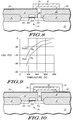
- FIGs. 4 and 9 each include a graph showing various materials and their oxidation states given the logarithm of partial pressure of oxygen at the material and the temperature of the material.
- FIGs. 7, 8, 10, and 11 each include a cross-sectional view of a portion of a substrate at various process steps in forming an electrode for a ferroelectric capacitor, wherein the electrode includes an elemental metal and its conductive metal oxide in accordance with another embodiment of the present invention.
- FIGs. 12-17 each include a cross-sectional view of a portion of a substrate illustrating a layer that includes an elemental metal and its conductive metal oxide in accordance with another embodiment of the present invention.
- The present invention includes a semiconductor device having a material including an elemental metal and its conductive metal oxide, wherein the material is capable of being oxidized or reduced preferentially to an adjacent region of the device. The material lessens the likelihood that the adjacent region is oxidized or reduced when this is undesired. A general description is followed by applications in which the material may be used. The applications that are described below are illustrative and are not meant to be limiting.
- Gibbs free energy changes are used to determine which material should be placed adjacent to a region to lessen the likelihood of oxidizing or reducing the region. For example, if the adjacent region is not to be reduced, the material should be more easily reduced compared to the adjacent region, and if the adjacent region is not to be oxidized, the material should be more easily oxidized compared to the adjacent region. Many materials cannot be used with this invention because a change in oxidation state changes the electrical properties of the material. For example, titanium is a conductor and can be oxidized to form a titanium oxide (TiOx where x is no more than two.) Titanium monoxide (TiO) is a semiconductor, and titanium dioxide (TiO₂) is an insulator. Therefore, the titanium material may change from a conductor to a semiconductor or an insulator or vice versa. These changes usually cause unwanted electrical characteristics within a semiconductor device. In order to avoid the transformation from a conductor to a semiconductor or an insulator or vice versa, the material in both its oxidized and reduced forms should either be both conductors, both semiconductors, or both insulators.
- A category of materials that may be used with the present invention are metals that can form conductive metal oxides. Ruthenium (Ru), rhenium (Re), iridium (Ir), and osmium (Os) are conductive and can be oxidized to form ruthenium dioxide (RuO₂), rhenium dioxide (ReO₂) or rhenium trioxide (ReO₃), iridium dioxide (IrO₂), and osmium tetraoxide (OsO₄), respectively, which are also conductive. Below illustrates the reaction for ruthenium:
Ru + O₂ ' RuO₂
The double-headed arrow indicates that the reaction is reversible. Ruthenium can be oxidized to form ruthenium dioxide, and ruthenium dioxide can be reduced to form ruthenium and oxygen. - The present invention requires a mixture of the metal and its conductive metal oxide. The mixture allows the reactions to be more freely reversible compared to having just the metal or just the conductive metal oxide. If both are not present, extra energy and more importantly longer times are needed to form a mixture. If the mixture is to be preferentially reduced, the mixture should have enough of the conductive metal oxide, such as RuO₂, to lessen the likelihood of reducing an adjacent region. If the mixture is to be preferentially oxidized, the mixture should have enough of the metal, such as Ru, to reduce the likelihood of oxidizing an adjacent layer. The present invention may be used in a variety of applications including substrate regions, silicon members, contact and via plugs, ferroelectric capacitors, and interconnects. As used hereinafter, "elemental metal" is a monatomic metallic material, such as Ru, Re, Ir, Os, Pb, Cu, and the like. Some elemental metals have conductive metal oxides, such as RuO₂, ReO₂, ReO₃, IrO₂, OsO₄, and the like. Descriptions of some applications follow.
- The present invention may be used with or as part of a contact or via plug within a semiconductor device. The plug may be used to lessen the likelihood that an underlying layer would be oxidized or reduced. FIG. 1 includes a cross-sectional view of a portion of a semiconductor device having a
substrate 10, a dopedregion 11 within thesubstrate 10, apatterned oxide layer 12, and asilicon plug 13. If the substrate would be oxidized, part of thesilicon plug 13 would form to a silicon dioxide layer. Before an interconnect is formed over theplug 13, the silicon dioxide layer would have to be removed. The removal of the silicon dioxide layer may also remove the part of the patternedoxide layer 12. Therefore, it is advantageous to protect thesilicon plug 13 prior to an oxidation step. - A
conductive layer 21 is formed over theoxide layer 12 and patterned to form a protective cap over thesilicon plug 13 as shown in FIG. 2. Theconductive layer 21 includes a mixture of an elemental metal and its conducive metal oxide.Layer 21 may be formed by sputter depositing using a target having a mixture of the elemental metal and the conductive metal oxide. When the layer includes Ru and RuO₂, about 5-95 percent of all of the atomic ruthenium in the sputter target is Ru and the balance of the atomic ruthenium in the target is RuO₂. In this case, the sputter target andlayer 21 have similar compositions.Layer 21 may be formed using other methods. For example, reactive ion sputtering using a Ru target and a plasma including oxygen may be used to depositlayer 21. In addition, a layer of Ru may be formed by sputter deposition or chemical vapor deposition and subsequently oxidized to convert only part of the Ru to RuO₂. In another embodiment, a layer of Ru and a layer of RuO₂ may be sequentially deposited. Additional layers of Ru and RuO₂ may be deposited. Regardless of the method used to formlayer 21, about 5-95 percent of all atomic ruthenium present inlayer 21 is Ru and balance of the atomic ruthenium in thelayer 21 is RuO₂. In other embodiments,layer 21 may include Re and any of its oxides, Ir and IrO₂, Os and OsO₄, or the like. As used in this specification, "Re and any of its oxides" includes Re and ReO₂, Re and ReO₃, or Re and ReO₂ and ReO₃. - A masking layer (not shown) is formed over the
layer 21 and patterned using a conventional lithographic technique. Thelayer 21 is patterned by ion milling the exposed portions of thelayer 21 or by plasma etching the exposed portions oflayer 21. If thelayer 21 includes Ru and RuO₂, the plasma etching chemistry may include oxygen or fluorine-containing compounds, such as carbon tetrafluoride (CF₄) and the like. If other materials are used, other etching chemistries may be used. After the patterning step, the masking layer (not shown) is removed. - As can be seen in FIG. 2, the
layer 21 covers thesilicon plug 13. Thelayer 21 lessens the likelihood that thesilicon plug 13 would be oxidized during a subsequent oxidation step. The Ru inlayer 21 may be oxidized to form RuO₂. In order forsilicon plug 13 to be oxidized under thelayer 21, oxygen must migrate through thelayer 21 before it reacts with the Ru inlayer 21. Also, thelayer 21 stays conductive even if the Ru is oxidized. A titanium layer cannot be used in place oflayer 21 because titanium, which is a conductor, oxidizes to become titanium dioxide, which is an insulator. In other embodiments, theplug 13 may include a metal and its conductive metal oxide instead of silicon. In this manner, thesubstrate 10 and theregion 11 may be better protected from oxidation, and electrical connections throughplug 13 may be maintained. - Both contact and via plugs may be formed using the present invention. For example, plug 13 shown in FIG. 1 may be comprise Ru and RuO₂ that may lessen the likelihood of oxidizing a region within the substrate adjacent to the
plug 13. Similarly, plug 13 may contact a silicon member, such as a gate electrode to prevent its oxidation. Ifplug 13 includes Ru and RuO₂,layer 21 shown in FIG. 2 is not needed. If hydrogen migration into regions within the substrate is a concern, about 5-95 atomic percent of all ruthenium within theplug 13 should be RuO₂. - The application of the present invention to interconnects is similar to that for contact or via plugs. FIG. 3 includes a cross-sectional view of a portion of an integrated circuit including: a
semiconductor substrate 10, a dopedregion 11 within thesubstrate 10, a first insulatinglayer 12 with a contact opening, a contact plug within the contact opening that includes atitanium nitride layer 141 and atungsten layer 142. A second insulatinglayer 143 overlies the first insulatinglayer 12 and the contact plug. The secondinsulating layer 143 includes an interconnecting channel. Amolybdenum layer 144 and acopper layer 145 are deposited over the second insulatinglayer 143 and within the interconnecting channel. The substrate is chemically-mechanically polished to remove portions of the molybdenum andcopper layers - A problem with copper is that it may be oxidized. Below illustrates the reactions for forming various copper compounds:
4 Cu + 2 O₂ ' 2 Cu₂O + O₂ ' 4 CuO
FIG. 4 includes a graph illustrating the relationship of the logarithm of partial pressure of oxygen and temperature to the reduction/oxidation of the copper compounds. The y-axis for the graph is the logarithm of oxygen partial pressure (Log pO2) when the pressure is in units of atmospheres. The graph has three curves, two of which are related to copper compounds. In the upper, left-hand part of the uppermost curve, the reaction conditions favor the formation of CuO. In the region between the uppermost and intermediate curve, the reaction conditions favor the formation of Cu₂O. In the lower, right-hand side of the intermediate curve, the reaction conditions favor the formation of Cu. For a given temperature and oxygen partial pressure, one can predict which product (Cu, Cu₂O, or CuO) should be formed. For example, if the temperature is about 400 degrees Kelvin and Log pO2 is about -60, Cu should be formed. Similarly, at about 400 degrees Kelvin and Log pO2 of about -20, CuO should be formed. The curve indicates that at higher temperatures, a higher oxygen partial pressure is needed to oxidize Cu. - The inventors believe that placing a material that is more readily oxidized than Cu lessens the likelihood that Cu is oxidized to Cu₂O or CuO. The lowermost curve in FIG 4 is for Re and ReO₂. This curve is similar to the copper-related curves previously discussed. It is noted that the curve for ReO₂/ReO₃ is not shown in FIG. 4, but it would lie between the Cu₂O/Cu curve and the Re/ReO₂ curve. FIG. 4 shows that Re is more readily oxidized to ReO₂ compared to Cu being oxidized to Cu₂O or CuO because Re oxidizes at a lower Log pO2 compared to Cu for a given temperature. Both Re and ReO₂ are conductive, and a layer of Re and ReO₂ may be used over the
interconnect 145 to lessen the likelihood that the Cu within theinterconnect 145 will be oxidized. - A
conductive layer 161 is formed over the molybdenum andcopper layers conductive layer 161 includes Re and ReO₂, wherein about 5-95 atomic percent of all atomic rhenium in the layer is Re and the balance of the atomic rhenium in the layer is ReO₂. The formation ofconductive layer 161 may be performed using the deposition and patterning methods previously described for Ru and RuO₂ except that ruthenium is being replaced by rhenium. Apassivation layer 171 is formed over theconductive layer 161 to form a substantially completed integrated circuit as shown in FIG. 6. Other layers and electrical connections (not shown) may be formed if needed. - The present invention may be used to lessen the likelihood of oxidizing or reducing other parts of a semiconductor device including a silicon-containing layer overlying the substrate, a dielectric layer overlying the substrate, a barrier layer overlying the substrate, and electrodes, such as gate electrodes or capacitor electrodes, overlying the substrate.
- The present invention may be used in forming ferroelectric capacitors. FIG. 7 includes a cross-sectional view of a portion of a semiconductor device that includes: a
semiconductor substrate 10; a metal-oxide-semiconductor transistor 30 having source/drain regions 301, agate dielectric layer 302, and agate electrode 303;field isolation regions 31 adjacent to thetransistor 30; a first planarized insulatinglayer 32, atitanium dioxide layer 33, acontact plug 34, and abottom electrode 35 that is about 500-2000 angstroms thick and comprises platinum. Conventional techniques are used to form the semiconductor device up to this point in the process. Thetitanium dioxide layer 33 and thebottom electrode 35 will contact a subsequently formed ferroelectric layer.Layer layer 33 must act as an insulator. In other embodiments,layer 33 may include oxides of magnesium, zirconium, tantalum, or the like.Electrode 35 must act as a conductor. In other embodiments,electrode 35 may include palladium, titanium nitride, metals and/or their conductive metal oxides (if the metal can form a conductive metal oxide), or the like. - A patterned
ferroelectric layer 41 about 700-2000 angstroms thick is formed over thebottom electrode 35 as shown in FIG. 8. Theferroelectric layer 41 includes lead zirconate titanate (PZT). It is noted that the word "zirconium" is sometimes used in place of "zirconate," but this is still the same material. The ferroelectric layer is deposited by spin coating, sputter depositing, or metalorganic chemical vapor deposition. The ferroelectric layer is annealed in an oxidizing ambient at about atmospheric pressure and a temperature in a range of 550-750 degrees Celsius. The annealing time is about 5-30 minutes if a furnace is used and about 10-300 seconds if a rapid thermal processor is used. The oxidizing ambient may include oxygen by itself or in combination with relatively inert gases, such as nitrogen, argon, helium, and the like. Non-oxidizing ambients, such as relatively inert gases without oxygen (nitrogen, argon, helium, or the like) and particularly reducing ambients, such as hydrogen, should be avoided unless the ferroelectric layer is subsequently annealed in an oxidizing ambient. - A masking layer (not shown) is formed over the
ferroelectric layer 41. Theferroelectric layer 41 is patterned by wet or dry etching techniques. Wet etching may be performed with a solution including hydrofluoric acid, nitric acid, and hydrogen peroxide. The solution is maintained at about room temperature during the etch. Dry etching may be performed using plasma etching or ion milling. For plasma etching, the etching chemistry should include oxygen, fluorine-containing compounds, such as carbon tetrafluoride (CF₄) and the like, and chlorine-containing compounds, such as carbon tetrachloride (CCl₄), molecular chlorine (Cl₂), and the like. After patterning, the masking layer (not shown) is removed to give the patternedferroelectric layer 41 as shown in FIG. 8. - As previously discussed, one problem with ferroelectric capacitors is their inability to retain their ferroelectric properties. Although the source of the problem is not known, it is possible that the ferroelectric layer is being at least partially reduced during subsequent processing. Of the materials in PZT, lead is the most readily reduced. FIG. 9 is similar to FIG. 4 except that the graph has one curve for elemental lead (Pb) and lead oxide (PbO) and one curve for Ru and RuO₂. The curve indicates that at higher temperatures, a higher oxygen partial pressure is needed to keep PbO from being reduced to Pb. FIG. 9 shows that RuO₂ is more readily reduced to Ru compared to PbO being reduced to Pb. Both Ru and RuO₂ are conductive, and both do not significantly react with PZT. Therefore, Ru and RuO₂ may be used as the top electrode for the ferroelectric capacitor. Similarly, Re and any of its oxides, Ir and IrO₂, Os and OsO₄, or the like, may used as the top electrode. The top electrode must include both the elemental metal and its conductive metal oxide.
- Referring to FIG. 10, a patterned
top electrode 61 is formed to cover the top and outer sides of theferroelectric layer 41. Thetop electrode 61 includes Ru and RuO₂, where about 5-95 percent of all of the atomic ruthenium in thetop electrode 61 is RuO₂ and the balance of the atomic ruthenium in thetop electrode 61 is Ru. It is noted that thetop electrode 61 has more RuO₂ concentration compared tolayer top electrode 61 is to protect the PZT in theferroelectric layer 41.Top electrode 61 is formed by sputter depositing a layer about 500-5000 angstroms thick using any of the methods previously described in forming thetop electrode 61. Similar methods are used if the layer includes Re and any of its oxides, Ir and IrO₂, Os and OsO₄, or the like. - A masking layer (not shown) is formed over the layer of Ru and RuO₂ and patterned using a conventional lithographic technique. The layer of Ru and RuO₂ is patterned by ion milling or by plasma etching the exposed portion of the layer. If the layer includes Ru and RuO₂, the plasma etching chemistry may include oxygen or fluorine-containing compounds, such as carbon tetrafluoride (CF₄) and the like. If other materials are used, other etching chemistries may be used. After the patterning step, the masking layer (not shown) is removed thereby leaving the
top electrode 61 as shown in FIG. 10. - As can be seen in FIG. 10, the
top electrode 61 protects the top and outer sides of theferroelectric layer 41. The RuO₂ in thetop electrode 61 may be reduced to form Ru. Thetop electrode 61 lessens the likelihood that theferroelectric layer 41 would be reduced during subsequent processing. In order forferroelectric layer 41 to be reduced, a reducing agent must migrate through thetop electrode 61 without reducing RuO₂. In this manner, theferroelectric layer 41 may be better protected from reduction. The other metals and their conductive metal oxides may be replaced by or used in conjunction with the layer of Ru and RuO₂. - A substantially completed integrated circuit is formed as shown in FIG. 11. A second
planarized insulation layer 71 is formed on thetitanium dioxide layer 33 and thetop electrode 61. An opening inlayer 71 is formed that extends to thetop electrode 61. A conductive plug is formed within the opening that includes atitanium nitride layer 72 and atungsten layer 73. Other materials may be used in the conductive plug, but the ability of the Ru and RuO₂ to oxidize and reduce may limit the choices. The material used for the conductive plug should remain conductive. Besides titanium nitride, the layer that contacts thetop electrode 61 may include titanium tungsten, tungsten, elemental metals and their conductive metal oxides, or the like. Aninterconnect 74 and apassivation layer 75 are formed over the conductive plug andlayer 71. Other interlevel insulating and interconnecting layers may be formed, if needed. Electrical connections to other parts of the integrated circuit, such as thegate electrode 303 and the left-hand source/drain region 301, are formed but are not shown in FIG 11. - The present invention may be used to form a protective layer. Although this embodiment is described in conjunction with a ferroelectric layer, the protective layer may be used for any number of devices. Silicon nitride is a good hydrogen barrier, but silicon nitride cannot come in direct contact with a PZT layer because of possible reactions between silicon and the PZT materials. Also, hydrogen may be produced during the formation of the silicon nitride layer, depending on the deposition chemistry chosen, that may reduce the oxide compounds within the ferroelectric layer. This application shows how a ferroelectric layer may be virtually encapsulated by protective layers including silicon nitride. FIG. 12 includes a cross-sectional view of a portion of semiconductor device that includes a first insulating
layer 80 and abottom electrode 81 that includes elemental iridium (Ir) or a mixture of Ir and iridium dioxide (IrO₂). Thebottom electrode 81 is deposited and patterned similar to the other layers previously described that include metals and their conductive metal oxides. A patterned second insulatinglayer 91 is formed over the first insulatinglayer 80 and part of thebottom electrode 81. A silicon nitride layer is deposited and anisotropically etched to formnitride sidewall spacers 92 as shown in FIG. 13. A layer of titanium dioxide is also deposited and anisotropically etched to formtitanium dioxide spacers 93 as shown in FIG. 13. In another embodiment, the titanium dioxide layer may be replaced or used in conjunction with oxides of magnesium, zirconium, tantalum, or the like. Optionally, the titanium dioxide layer does not need to be anisotropically etched, but covers all of the exposed surfaces of the semiconductor device. This optional embodiment is not shown in FIG. 13. During the formation of the spacers, hydrogen may have been generated and reduced IrO₂, if any was originally present. A short anneal using an oxidizing ambient may be performed, if needed, to oxidize some of the Ir to IrO₂. After spacer formation, IrO₂ should make up between 5-95 atomic percent of all of the iridium within thebottom electrode 81. - A
ferroelectric layer 101 is formed that includes lanthanum-doped PZT as seen in FIG. 14. Theferroelectric layer 101 is deposited by one of the methods previously discussed in conjunction with layers that include PZT. The substrate including theferroelectric layer 101 is patterned by chemical-mechanical polishing. To ensure that all of theferroelectric layer 101 over the insulatinglayer 91 is removed, theferroelectric layer 101 is wet etched using a solution including hydrofluoric acid, nitric acid, and hydrogen peroxide. In addition to removing any residualferroelectric layer 101, the wet etching step also etches some of theferroelectric layer 101 within the opening to make certain that theferroelectric layer 101 only contacts thetitanium dioxide spacers 93 and thebottom electrode 81. The substrate including theferroelectric layer 101 is annealed in a manner similar to theferroelectric layer 41 that was previously described. - A
top electrode 111 is formed and includes elemental osmium (Os) and osmium tetraoxide (OsO₄) as seen in FIG. 15. The OsO₄ makes up about 5-95 atomic percent of the total osmium in thetop electrode 111, and the balance of the osmium in thetop electrode 111 is Os. Thetop electrode 111 is deposited and patterned similar to the other layers previous described that include metals and their conductive metal oxides. Other layers and electrical connections are made to the ferroelectric capacitor, but are not shown in the figures. - In this embodiment, the ferroelectric layer has
electrodes Nitride spacers 92 surround the sides of theferroelectric layer 101 but do not contact theferroelectric layer 101. Hydrogen should not contact theferroelectric layer 101 via the sides because thenitride spacers 92 should act as a hydrogen barrier. Theferroelectric layer 101 was not reduced by hydrogen that is produced during the nitride spacer formation because thenitride spacers 92 were formed prior to theferroelectric layer 101. Thetitanium dioxide spacers 93 separate thenitride spacers 92 and theferroelectric layer 101. Therefore, the silicon within thenitride spacers 92 should not react with theferroelectric layer 101. Theelectrodes silicon nitride spacers 92 virtually encapsulate theferroelectric layer 101. With this embodiment, reduction of theferroelectric layer 101 is less likely than with conventional ferroelectric capacitors. - FIG. 16 includes another embodiment having a protected ferroelectric layer. FIG. 16 has an
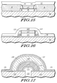
oxide layer 80 and a firstsilicon nitride layer 81. Aconductive layer 121, which includes Re and ReO₂, and aferroelectric layer 122, which includes PZT, are formed over the firstsilicon nitride layer 81. Theconductive layer 121 acts as the bottom electrode, and ReO₂ within theconductive layer 121 lessens the likelihood of reducing theferroelectric layer 122. Thelayers layers titanium dioxide layer 123 and a secondsilicon nitride layer 124 are formed over the insulatinglayer 80 including thelayers layers ferroelectric layer 122 is an annealed in an oxidizing ambient. This anneal is similar to the anneal used forferroelectric layer 41 that was previously described. Atop electrode 125 including Ru and RuO₂ is formed over theferroelectric layer 122 and the sidewall spacers. RuO₂ within thetop electrode 125 lessens the likelihood of reducing theferroelectric layer 122. Both theconductive layer 121, which acts as the bottom electrode, and theferroelectric layer 122 are virtually encapsulated by the firstsilicon nitride layer 81, the secondsilicon nitride layer 124 of the sidewall spacers, and thetop electrode 125. Because it is not completely known if the degradation problems with ferroelectric capacitors are related to the bottom electrode or the ferroelectric layer, this embodiment may be effective against degradation problems since the bottom electrode and ferroelectric layer are more encapsulated than in other embodiments. - FIG. 17 includes a cross-sectional view of a portion of a semiconductor device having a ferroelectric capacitor and shielding layers to protect the ferroelectric capacitors from reducing agents. The substrate includes a first insulating
layer 130 and atitanium dioxide layer 131. Apolysilicon plug 132 is covered by a firstconductive layer 133, such as Ru and RuO₂) that defines the first electrode of the capacitor. Aferroelectric layer 134 lies over the firstconductive layer 133, and aplatinum layer 135 lies over theferroelectric layer 134. Theplatinum layer 135 acts as the second electrode for the capacitor. The formation of the device up to this point in the process, including the anneal of theferroelectric layer 134, are conventional. A second insulatinglayer 136 is formed over the electrode and is thick enough so that there is little, if any, capacitive coupling between theplatinum layer 135 and subsequently formed shielding layer. Typically, thesecond insulation layer 136 is at least about 5000 angstroms thick. The substrate including the second insulatinglayer 136 is annealed in an oxidizing ambient to lessen the amount of hydrogen that may be trapped within the second insulatinglayer 136. - Shielding layers 137 and 138 are formed over the second insulating
layer 136.Shielding layer 137 includes a mixture of Ru and RuO₂ similar tolayer 61.Shielding layer 138 includes silicon nitride and is formed by sputter deposition or plasma-enhanced chemical vapor deposition. The temperature and amount of hydrogen present during the silicon nitride deposition should be relatively low to minimize the reduction of RuO₂ to Ru withinlayer 137. After deposition oflayer 138, the substrate is annealed in an oxidizing ambient to help oxidize some of the Ru withinlayer 137 and to seal any pinholes that may be present withinlayer 138. For a reducing agent, such as hydrogen, to interfere with the ferroelectric capacitor, the reducing agent must not only pass throughlayer 138 but also pass throughlayer 137 without reducing the RuO₂ to Ru withinlayer 137. This embodiment not only illustrates a good hydrogen barrier, but also shows that the shielding layers do not have to electrically participate in the semiconductor device if this is so desired. - In the foregoing specification, the invention has been described with reference to specific embodiments thereof. However, it will be evident that various modifications and changes can be made thereto without departing from the broader spirit or scope of the invention as set forth in the appended claims. The specification and drawings are, accordingly, to be regarded in an illustrative rather than a restrictive sense.
Claims (10)
- A semiconductor device comprising:
a substrate (10, 80) having a primary surface;
a first region at a location selected from a group consisting of:
a location (11) lying within the substrate adjacent to the primary surface; and
a location (132, 41, 101, 122, 134, 135, 132, 41, 101, 122, 135, 141, 144, 145) overlying the substrate; and
a first layer (21, 161, 61, 81, 111, 121, 125, 133, and 137) overlying the first region,
characterized in that:
the first layer includes an elemental metal and its conductive metal oxide;
the elemental metal is capable of being oxidized to the conductive metal oxide in an oxidation;
the conductive metal oxide is capable of being reduced to the elemental metal in a reduction;
the oxidation and the reduction are reversible reactions; and
the first layer reacts in one of the reversible reactions preferentially to the first region reacting in a first reaction. - The device of claim 1, further characterized in that the elemental metal and its conductive metal oxide are:
ruthenium and ruthenium dioxide;
rhenium and any of its oxides;
iridium and iridium dioxide; or
osmium and osmium tetraoxide. - The device of claim 1, further characterized in that:
the first region is a region within the substrate (11), a silicon-containing layer overlying the substrate (132), a dielectric layer (41, 101,122, 134), an electrode (135), a barrier layer (141 and 144), a contact plug (13, 142, 34, and 132), a via plug, or an interconnect (145); and
the elemental metal is capable of being oxidized to the conductive metal oxide preferentially to the first region being oxidized. - The device of claim 1, further characterized in that:
the first region is a ferroelectric layer (41, 101, 122, and 134); and
the conductive metal oxide is capable of being reduced to the element metal preferentially to the ferroelectric layer being reduced. - A semiconductor device comprising:
a substrate having a primary surface;
a first region that is selected from a group consisting of a region within the substrate (11), a silicon-containing layer overlying the substrate (132), an electrode (135), a barrier layer overlying the substrate (141 and 144), a contact plug overlying the substrate (13, 142, 34, and 132), a via plug overlying the substrate, and an interconnect overlying the substrate (145);
a first layer (21, 161, 121, 133, and 137) overlying the first region,
characterized in that the first layer includes an elemental metal and its conductive metal oxide, wherein the elemental metal is capable of being oxidized to its conductive metal oxide preferentially to the first region being oxidized. - The device of claim 5, further characterized in that:
the first layer has a plurality of first atoms;
the conductive metal oxide has a plurality of first atoms;
and
at least 5 atomic percent of the first atoms within the first layer are in the elemental metal. - The device of claim 5, further characterized in that:
the first region is an interconnect (145) that includes copper; and
the elemental metal is rhenium. - A ferroelectric capacitor comprising:
a ferroelectric layer (41, 101, 122, and 134); and
a first layer (61, 111, 125, and 137) overlying the ferroelectric layer,
characterized in that:
the first layer includes an elemental metal and its conductive metal oxide; and
the conductive metal oxide is capable of being reduced to the elemental metal preferentially to the ferroelectric layer being reduced. - The ferroelectric capacitor of claim 8, further characterized in that:
the first layer (61, 111, 125, and 137) has a plurality of first atoms;
the conductive metal oxide has a plurality of first atoms;
and
at least 5 atomic percent of the first atoms within the first layer are in the conductive metal oxide. - The ferroelectric capacitor of claim 8, further characterized in that:
the ferroelectric layer (61, 111, 125, and 137) includes lead; and
the elemental metal includes ruthenium.
Applications Claiming Priority (2)
| Application Number | Priority Date | Filing Date | Title |
|---|---|---|---|
| US08/072,012 US5407855A (en) | 1993-06-07 | 1993-06-07 | Process for forming a semiconductor device having a reducing/oxidizing conductive material |
| US72012 | 1993-06-07 |
Publications (2)
| Publication Number | Publication Date |
|---|---|
| EP0629002A1 true EP0629002A1 (en) | 1994-12-14 |
| EP0629002B1 EP0629002B1 (en) | 2004-03-03 |
Family
ID=22105010
Family Applications (1)
| Application Number | Title | Priority Date | Filing Date |
|---|---|---|---|
| EP94108641A Expired - Lifetime EP0629002B1 (en) | 1993-06-07 | 1994-06-06 | Process for forming a semiconductor device |
Country Status (8)
| Country | Link |
|---|---|
| US (2) | US5407855A (en) |
| EP (1) | EP0629002B1 (en) |
| JP (1) | JPH0799290A (en) |
| KR (1) | KR100354578B1 (en) |
| CN (1) | CN1093319C (en) |
| DE (1) | DE69433582T2 (en) |
| SG (1) | SG69959A1 (en) |
| TW (1) | TW278208B (en) |
Cited By (11)
| Publication number | Priority date | Publication date | Assignee | Title |
|---|---|---|---|---|
| US5407855A (en) * | 1993-06-07 | 1995-04-18 | Motorola, Inc. | Process for forming a semiconductor device having a reducing/oxidizing conductive material |
| EP0740342A2 (en) * | 1995-04-28 | 1996-10-30 | Rohm Co., Ltd. | Semiconductor device and wiring method |
| US5973342A (en) * | 1996-04-25 | 1999-10-26 | Rohm Co., Ltd. | Semiconductor device having an iridium electrode |
| EP1006583A1 (en) * | 1998-12-01 | 2000-06-07 | Rohm Co., Ltd. | Ferroelectric memory device and method for manufacturing same |
| EP1017096A2 (en) * | 1998-12-28 | 2000-07-05 | Sharp Kabushiki Kaisha | Method of fabricating semiconductor memory device |
| EP1113493A1 (en) * | 2000-01-03 | 2001-07-04 | Infineon Technologies AG | Process of fabrication of a ferroelectric semiconductor memory |
| EP1150340A1 (en) * | 2000-04-27 | 2001-10-31 | Sharp Kabushiki Kaisha | Semiconductor device producing method and semiconducor device |
| EP1182698A3 (en) * | 2000-08-24 | 2002-07-24 | Infineon Technologies AG | Barrier layer for a storage capacitor |
| DE19620022C2 (en) * | 1995-05-17 | 2002-09-19 | Hyundai Electronics Ind | Method for producing a diffusion barrier metal layer in a semiconductor device |
| WO2003092051A2 (en) * | 2002-04-26 | 2003-11-06 | Infineon Technologies Ag | Barrier for capacitor over plug structures |
| WO2006039219A1 (en) * | 2004-09-30 | 2006-04-13 | Tokyo Electron Limited | A method and system for forming a passivated metal layer |
Families Citing this family (114)
| Publication number | Priority date | Publication date | Assignee | Title |
|---|---|---|---|---|
| US5439840A (en) * | 1993-08-02 | 1995-08-08 | Motorola, Inc. | Method of forming a nonvolatile random access memory capacitor cell having a metal-oxide dielectric |
| US6052271A (en) * | 1994-01-13 | 2000-04-18 | Rohm Co., Ltd. | Ferroelectric capacitor including an iridium oxide layer in the lower electrode |
| JP2956485B2 (en) * | 1994-09-07 | 1999-10-04 | 日本電気株式会社 | Method for manufacturing semiconductor device |
| US5563762A (en) * | 1994-11-28 | 1996-10-08 | Northern Telecom Limited | Capacitor for an integrated circuit and method of formation thereof, and a method of adding on-chip capacitors to an integrated circuit |
| US6271077B1 (en) | 1995-03-27 | 2001-08-07 | Fujitsu Limited | Thin film deposition method, capacitor device and method for fabricating the same, and semiconductor device and method for fabricating the same |
| US5874364A (en) | 1995-03-27 | 1999-02-23 | Fujitsu Limited | Thin film deposition method, capacitor device and method for fabricating the same, and semiconductor device and method for fabricating the same |
| KR0147639B1 (en) * | 1995-05-29 | 1998-08-01 | 김광호 | High dielectronics capacitor electrode & its fabrication method |
| CN1054702C (en) * | 1995-06-26 | 2000-07-19 | 现代电子产业株式会社 | Method for producing semiconductor device capacitor |
| US5739049A (en) * | 1995-08-21 | 1998-04-14 | Hyundai Electronics Industries Co., Ltd. | Method for fabricating semiconductor device having a capacitor and a method of forming metal wiring on a semiconductor substrate |
| US5631804A (en) * | 1995-11-13 | 1997-05-20 | Micron Technology, Inc. | Contact fill capacitor having a sidewall that connects the upper and lower surfaces of the dielectric and partially surrounds an insulating layer |
| KR100200299B1 (en) * | 1995-11-30 | 1999-06-15 | 김영환 | Method for manufacturing capacitor of semiconductor device |
| US6388272B1 (en) | 1996-03-07 | 2002-05-14 | Caldus Semiconductor, Inc. | W/WC/TAC ohmic and rectifying contacts on SiC |
| US5929523A (en) * | 1996-03-07 | 1999-07-27 | 3C Semiconductor Corporation | Os rectifying Schottky and ohmic junction and W/WC/TiC ohmic contacts on SiC |
| US5926359A (en) * | 1996-04-01 | 1999-07-20 | International Business Machines Corporation | Metal-insulator-metal capacitor |
| US5744376A (en) * | 1996-04-08 | 1998-04-28 | Chartered Semiconductor Manufacturing Pte, Ltd | Method of manufacturing copper interconnect with top barrier layer |
| US6100196A (en) * | 1996-04-08 | 2000-08-08 | Chartered Semiconductor Manufacturing Ltd. | Method of making a copper interconnect with top barrier layer |
| JP3388089B2 (en) * | 1996-04-25 | 2003-03-17 | シャープ株式会社 | Method of manufacturing nonvolatile semiconductor memory device |
| US5807774A (en) * | 1996-12-06 | 1998-09-15 | Sharp Kabushiki Kaisha | Simple method of fabricating ferroelectric capacitors |
| JP3452763B2 (en) | 1996-12-06 | 2003-09-29 | シャープ株式会社 | Semiconductor storage device and method of manufacturing semiconductor storage device |
| JP3454058B2 (en) * | 1996-12-11 | 2003-10-06 | 富士通株式会社 | Semiconductor memory and manufacturing method thereof |
| JP3299909B2 (en) * | 1997-02-25 | 2002-07-08 | シャープ株式会社 | Multilayer structure electrode using oxide conductor |
| US5773314A (en) * | 1997-04-25 | 1998-06-30 | Motorola, Inc. | Plug protection process for use in the manufacture of embedded dynamic random access memory (DRAM) cells |
| US6287637B1 (en) * | 1997-07-18 | 2001-09-11 | Ramtron International Corporation | Multi-layer approach for optimizing ferroelectric film performance |
| JP3484324B2 (en) | 1997-07-29 | 2004-01-06 | シャープ株式会社 | Semiconductor memory device |
| US5910880A (en) * | 1997-08-20 | 1999-06-08 | Micron Technology, Inc. | Semiconductor circuit components and capacitors |
| JP3090198B2 (en) * | 1997-08-21 | 2000-09-18 | 日本電気株式会社 | Structure of semiconductor device and method of manufacturing the same |
| JP3319994B2 (en) * | 1997-09-29 | 2002-09-03 | シャープ株式会社 | Semiconductor storage element |
| JPH11111753A (en) * | 1997-10-01 | 1999-04-23 | Mitsubishi Electric Corp | Semiconductor device |
| JP3445925B2 (en) * | 1997-10-07 | 2003-09-16 | シャープ株式会社 | Method for manufacturing semiconductor storage element |
| US6130102A (en) * | 1997-11-03 | 2000-10-10 | Motorola Inc. | Method for forming semiconductor device including a dual inlaid structure |
| JPH11145410A (en) * | 1997-11-13 | 1999-05-28 | Toshiba Corp | Semiconductor device and its manufacture |
| JP3212930B2 (en) * | 1997-11-26 | 2001-09-25 | 日本電気株式会社 | Capacity and manufacturing method thereof |
| JP2001511318A (en) * | 1997-12-10 | 2001-08-07 | コーニンクレッカ フィリップス エレクトロニクス エヌ ヴィ | Semiconductor device and manufacturing method thereof |
| US6344413B1 (en) | 1997-12-22 | 2002-02-05 | Motorola Inc. | Method for forming a semiconductor device |
| KR100436058B1 (en) | 1997-12-27 | 2004-12-17 | 주식회사 하이닉스반도체 | Method for forming ferroelectric capacitor to prevent ferroelectric characteristic from being deteriorated |
| KR100533991B1 (en) | 1997-12-27 | 2006-05-16 | 주식회사 하이닉스반도체 | Manufacturing method of high dielectric capacitor of semiconductor device |
| KR100458084B1 (en) * | 1997-12-27 | 2005-06-07 | 주식회사 하이닉스반도체 | Ferroelectric Capacitor Formation Method with Lower Electrode with Reduced Leakage Current |
| JP3976288B2 (en) * | 1998-01-21 | 2007-09-12 | ローム株式会社 | Semiconductor device and manufacturing method of semiconductor device |
| KR100404649B1 (en) * | 1998-02-23 | 2003-11-10 | 가부시끼가이샤 히다치 세이사꾸쇼 | Semiconductor device and fabrication method thereof |
| US6191443B1 (en) | 1998-02-28 | 2001-02-20 | Micron Technology, Inc. | Capacitors, methods of forming capacitors, and DRAM memory cells |
| US6162744A (en) * | 1998-02-28 | 2000-12-19 | Micron Technology, Inc. | Method of forming capacitors having high-K oxygen containing capacitor dielectric layers, method of processing high-K oxygen containing dielectric layers, method of forming a DRAM cell having having high-K oxygen containing capacitor dielectric layers |
| JP3116897B2 (en) * | 1998-03-18 | 2000-12-11 | 日本電気株式会社 | Fine wiring formation method |
| US6156638A (en) | 1998-04-10 | 2000-12-05 | Micron Technology, Inc. | Integrated circuitry and method of restricting diffusion from one material to another |
| US6730559B2 (en) | 1998-04-10 | 2004-05-04 | Micron Technology, Inc. | Capacitors and methods of forming capacitors |
| US6130103A (en) * | 1998-04-17 | 2000-10-10 | Symetrix Corporation | Method for fabricating ferroelectric integrated circuits |
| US5998258A (en) * | 1998-04-22 | 1999-12-07 | Motorola, Inc. | Method of forming a semiconductor device having a stacked capacitor structure |
| US6181012B1 (en) | 1998-04-27 | 2001-01-30 | International Business Machines Corporation | Copper interconnection structure incorporating a metal seed layer |
| US6165834A (en) * | 1998-05-07 | 2000-12-26 | Micron Technology, Inc. | Method of forming capacitors, method of processing dielectric layers, method of forming a DRAM cell |
| US6255186B1 (en) | 1998-05-21 | 2001-07-03 | Micron Technology, Inc. | Methods of forming integrated circuitry and capacitors having a capacitor electrode having a base and a pair of walls projecting upwardly therefrom |
| JPH11354637A (en) * | 1998-06-11 | 1999-12-24 | Oki Electric Ind Co Ltd | Connection structure for wiring and formation of connection part of the wiring |
| US6156619A (en) | 1998-06-29 | 2000-12-05 | Oki Electric Industry Co., Ltd. | Semiconductor device and method of fabricating |
| US5918120A (en) * | 1998-07-24 | 1999-06-29 | Taiwan Semiconductor Manufacturing Company, Ltd. | Method for fabricating capacitor-over-bit line (COB) dynamic random access memory (DRAM) using tungsten landing plug contacts and Ti/TiN bit lines |
| US6452271B2 (en) | 1998-07-31 | 2002-09-17 | Micron Technology, Inc. | Interconnect component for a semiconductor die including a ruthenium layer and a method for its fabrication |
| US6271131B1 (en) | 1998-08-26 | 2001-08-07 | Micron Technology, Inc. | Methods for forming rhodium-containing layers such as platinum-rhodium barrier layers |
| US6541067B1 (en) * | 1998-08-27 | 2003-04-01 | Micron Technology, Inc. | Solvated ruthenium precursors for direct liquid injection of ruthenium and ruthenium oxide and method of using same |
| US6133159A (en) | 1998-08-27 | 2000-10-17 | Micron Technology, Inc. | Methods for preparing ruthenium oxide films |
| US6074945A (en) * | 1998-08-27 | 2000-06-13 | Micron Technology, Inc. | Methods for preparing ruthenium metal films |
| US6197628B1 (en) | 1998-08-27 | 2001-03-06 | Micron Technology, Inc. | Ruthenium silicide diffusion barrier layers and methods of forming same |
| US5962716A (en) | 1998-08-27 | 1999-10-05 | Micron Technology, Inc. | Methods for preparing ruthenium and osmium compounds |
| US6517616B2 (en) * | 1998-08-27 | 2003-02-11 | Micron Technology, Inc. | Solvated ruthenium precursors for direct liquid injection of ruthenium and ruthenium oxide |
| US6284655B1 (en) | 1998-09-03 | 2001-09-04 | Micron Technology, Inc. | Method for producing low carbon/oxygen conductive layers |
| US6239028B1 (en) | 1998-09-03 | 2001-05-29 | Micron Technology, Inc. | Methods for forming iridium-containing films on substrates |
| US6323081B1 (en) | 1998-09-03 | 2001-11-27 | Micron Technology, Inc. | Diffusion barrier layers and methods of forming same |
| US6204203B1 (en) * | 1998-10-14 | 2001-03-20 | Applied Materials, Inc. | Post deposition treatment of dielectric films for interface control |
| US6537461B1 (en) * | 2000-04-24 | 2003-03-25 | Hitachi, Ltd. | Process for treating solid surface and substrate surface |
| JP3114710B2 (en) | 1998-11-30 | 2000-12-04 | 日本電気株式会社 | Ferroelectric memory and method of manufacturing the same |
| US20010013660A1 (en) * | 1999-01-04 | 2001-08-16 | Peter Richard Duncombe | Beol decoupling capacitor |
| JP4221100B2 (en) * | 1999-01-13 | 2009-02-12 | エルピーダメモリ株式会社 | Semiconductor device |
| US6320263B1 (en) * | 1999-02-18 | 2001-11-20 | Advanced Micro Devices, Inc. | Semiconductor metalization barrier and manufacturing method therefor |
| US6316797B1 (en) * | 1999-02-19 | 2001-11-13 | Advanced Technology Materials, Inc. | Scalable lead zirconium titanate(PZT) thin film material and deposition method, and ferroelectric memory device structures comprising such thin film material |
| US6421223B2 (en) * | 1999-03-01 | 2002-07-16 | Micron Technology, Inc. | Thin film structure that may be used with an adhesion layer |
| US6348709B1 (en) * | 1999-03-15 | 2002-02-19 | Micron Technology, Inc. | Electrical contact for high dielectric constant capacitors and method for fabricating the same |
| US6329286B1 (en) | 1999-04-27 | 2001-12-11 | Micron Technology, Inc. | Methods for forming conformal iridium layers on substrates |
| US6190963B1 (en) * | 1999-05-21 | 2001-02-20 | Sharp Laboratories Of America, Inc. | Composite iridium-metal-oxygen barrier structure with refractory metal companion barrier and method for same |
| KR100333667B1 (en) | 1999-06-28 | 2002-04-24 | 박종섭 | Method for fabricating capacitor of ferroelectric random access memory device |
| DE19937503C1 (en) * | 1999-08-09 | 2001-01-04 | Siemens Ag | Etching oxide films of a ferroelectric bismuth-containing mixed oxide comprises applying an oxide film to a substrate, contacting with an etching solution, and removing the etching solution |
| JP3545279B2 (en) * | 1999-10-26 | 2004-07-21 | 富士通株式会社 | Ferroelectric capacitor, method of manufacturing the same, and semiconductor device |
| JP2001144090A (en) * | 1999-11-11 | 2001-05-25 | Nec Corp | Method of manufacturing semiconductor device |
| US7005695B1 (en) * | 2000-02-23 | 2006-02-28 | Micron Technology, Inc. | Integrated circuitry including a capacitor with an amorphous and a crystalline high K capacitor dielectric region |
| US6380080B2 (en) | 2000-03-08 | 2002-04-30 | Micron Technology, Inc. | Methods for preparing ruthenium metal films |
| US7061111B2 (en) * | 2000-04-11 | 2006-06-13 | Micron Technology, Inc. | Interconnect structure for use in an integrated circuit |
| US6420267B1 (en) * | 2000-04-18 | 2002-07-16 | Infineon Technologies Ag | Method for forming an integrated barrier/plug for a stacked capacitor |
| US6429127B1 (en) * | 2000-06-08 | 2002-08-06 | Micron Technology, Inc. | Methods for forming rough ruthenium-containing layers and structures/methods using same |
| US6423632B1 (en) | 2000-07-21 | 2002-07-23 | Motorola, Inc. | Semiconductor device and a process for forming the same |
| US6660631B1 (en) * | 2000-08-31 | 2003-12-09 | Micron Technology, Inc. | Devices containing platinum-iridium films and methods of preparing such films and devices |
| JP4025829B2 (en) | 2000-09-18 | 2007-12-26 | 富士通株式会社 | Semiconductor device and manufacturing method thereof |
| US6958508B2 (en) | 2000-10-17 | 2005-10-25 | Matsushita Electric Industrial Co., Ltd. | Ferroelectric memory having ferroelectric capacitor insulative film |
| JP2002260951A (en) * | 2000-12-28 | 2002-09-13 | Denso Corp | Laminated dielectric element and its manufacturing method and paste material for electrode |
| KR100359299B1 (en) * | 2001-03-26 | 2002-11-07 | Samsung Electronics Co Ltd | Semiconductor memory device having resist pattern and method for forming metal contact thereof |
| US6531324B2 (en) * | 2001-03-28 | 2003-03-11 | Sharp Laboratories Of America, Inc. | MFOS memory transistor & method of fabricating same |
| JP2004524778A (en) * | 2001-04-11 | 2004-08-12 | キョウセラ ワイヤレス コーポレイション | Tunable matching circuit |
| US20030042614A1 (en) * | 2001-08-30 | 2003-03-06 | Ammar Deraa | Metal silicide adhesion layer for contact structures |
| US6858904B2 (en) * | 2001-08-30 | 2005-02-22 | Micron Technology, Inc. | High aspect ratio contact structure with reduced silicon consumption |
| US6787831B2 (en) * | 2002-01-15 | 2004-09-07 | Infineon Technologies Aktiengesellschaft | Barrier stack with improved barrier properties |
| JP4636834B2 (en) * | 2002-11-13 | 2011-02-23 | パナソニック株式会社 | Semiconductor device and manufacturing method thereof |
| US7026714B2 (en) * | 2003-03-18 | 2006-04-11 | Cunningham James A | Copper interconnect systems which use conductive, metal-based cap layers |
| WO2005074032A1 (en) * | 2004-01-28 | 2005-08-11 | Fujitsu Limited | Semiconductor device and its manufacturing method |
| KR100881717B1 (en) * | 2006-12-27 | 2009-02-06 | 주식회사 하이닉스반도체 | Capacitor and method for manufacturing the same |
| US8298909B2 (en) | 2006-12-27 | 2012-10-30 | Hynix Semiconductor Inc. | Semiconductor device and method for fabricating the same |
| KR100823168B1 (en) * | 2007-01-08 | 2008-04-18 | 삼성전자주식회사 | Ferroelectric memory device and method for forming the same |
| JP2008218782A (en) | 2007-03-06 | 2008-09-18 | Seiko Epson Corp | Semiconductor device and its manufacturing method |
| US7655556B2 (en) | 2007-03-23 | 2010-02-02 | Taiwan Semiconductor Manufacturing Company, Ltd. | Interconnect structures for semiconductor devices |
| US9385034B2 (en) * | 2007-04-11 | 2016-07-05 | Taiwan Semiconductor Manufacturing Company, Ltd. | Carbonization of metal caps |
| KR100869343B1 (en) | 2007-08-31 | 2008-11-19 | 주식회사 하이닉스반도체 | Method for manufacturing capacitor in semiconductor device |
| KR20090074396A (en) * | 2008-01-02 | 2009-07-07 | 삼성전자주식회사 | Information storage media using ferroelectric material, manufacturing method of the information storage media, and information storage device adopting the same |
| CN101630667A (en) * | 2008-07-15 | 2010-01-20 | 中芯国际集成电路制造(上海)有限公司 | Method and system for forming conductive bump with copper interconnections |
| US8120117B2 (en) * | 2009-05-01 | 2012-02-21 | Kabushiki Kaisha Toshiba | Semiconductor device with metal gate |
| US20140179512A1 (en) * | 2012-12-20 | 2014-06-26 | Sunpower Technologies Llc | Photocatalyst for the production of hydrogen |
| CN103219225A (en) * | 2013-03-29 | 2013-07-24 | 河北大学 | Barrier layer material for silicon-based ferroelectric capacitor integration and integrating method |
| US10727070B2 (en) | 2016-03-21 | 2020-07-28 | International Business Machines Corporation | Liner-less contact metallization |
| US9653311B1 (en) * | 2016-05-13 | 2017-05-16 | Applied Materials, Inc. | 3D NAND staircase CD fabrication utilizing ruthenium material |
| US10312137B2 (en) | 2016-06-07 | 2019-06-04 | Applied Materials, Inc. | Hardmask layer for 3D NAND staircase structure in semiconductor applications |
| JP7330046B2 (en) * | 2019-09-30 | 2023-08-21 | 東京エレクトロン株式会社 | SUBSTRATE PROCESSING METHOD AND SUBSTRATE PROCESSING APPARATUS |
| US11177171B2 (en) | 2019-10-01 | 2021-11-16 | International Business Machines Corporation | Encapsulated top via interconnects |
Citations (4)
| Publication number | Priority date | Publication date | Assignee | Title |
|---|---|---|---|---|
| US4851895A (en) * | 1985-05-06 | 1989-07-25 | American Telephone And Telegraph Company, At&T Bell Laboratories | Metallization for integrated devices |
| EP0409018A2 (en) * | 1989-07-17 | 1991-01-23 | National Semiconductor Corporation | Electrodes for electrical ceramic oxide devices |
| EP0478799A1 (en) * | 1990-04-24 | 1992-04-08 | Ramtron International Corporation | Semiconductor device having ferroelectric material and method of producing the same |
| JPH04364759A (en) * | 1991-06-12 | 1992-12-17 | Kawasaki Steel Corp | Semiconductor device and manufacture thereof |
Family Cites Families (7)
| Publication number | Priority date | Publication date | Assignee | Title |
|---|---|---|---|---|
| US3657029A (en) * | 1968-12-31 | 1972-04-18 | Texas Instruments Inc | Platinum thin-film metallization method |
| US5005102A (en) * | 1989-06-20 | 1991-04-02 | Ramtron Corporation | Multilayer electrodes for integrated circuit capacitors |
| US5003428A (en) * | 1989-07-17 | 1991-03-26 | National Semiconductor Corporation | Electrodes for ceramic oxide capacitors |
| US5122923A (en) * | 1989-08-30 | 1992-06-16 | Nec Corporation | Thin-film capacitors and process for manufacturing the same |
| US5142437A (en) * | 1991-06-13 | 1992-08-25 | Ramtron Corporation | Conducting electrode layers for ferroelectric capacitors in integrated circuits and method |
| US5285017A (en) * | 1991-12-31 | 1994-02-08 | Intel Corporation | Embedded ground plane and shielding structures using sidewall insulators in high frequency circuits having vias |
| US5407855A (en) * | 1993-06-07 | 1995-04-18 | Motorola, Inc. | Process for forming a semiconductor device having a reducing/oxidizing conductive material |
-
1993
- 1993-06-07 US US08/072,012 patent/US5407855A/en not_active Expired - Lifetime
-
1994
- 1994-04-21 TW TW083103556A patent/TW278208B/zh not_active IP Right Cessation
- 1994-06-04 CN CN94106509A patent/CN1093319C/en not_active Expired - Lifetime
- 1994-06-06 SG SG1996003545A patent/SG69959A1/en unknown
- 1994-06-06 DE DE69433582T patent/DE69433582T2/en not_active Expired - Lifetime
- 1994-06-06 EP EP94108641A patent/EP0629002B1/en not_active Expired - Lifetime
- 1994-06-07 KR KR1019940012702A patent/KR100354578B1/en not_active IP Right Cessation
- 1994-06-07 JP JP6147041A patent/JPH0799290A/en active Pending
- 1994-11-18 US US08/342,293 patent/US5510651A/en not_active Expired - Lifetime
Patent Citations (4)
| Publication number | Priority date | Publication date | Assignee | Title |
|---|---|---|---|---|
| US4851895A (en) * | 1985-05-06 | 1989-07-25 | American Telephone And Telegraph Company, At&T Bell Laboratories | Metallization for integrated devices |
| EP0409018A2 (en) * | 1989-07-17 | 1991-01-23 | National Semiconductor Corporation | Electrodes for electrical ceramic oxide devices |
| EP0478799A1 (en) * | 1990-04-24 | 1992-04-08 | Ramtron International Corporation | Semiconductor device having ferroelectric material and method of producing the same |
| JPH04364759A (en) * | 1991-06-12 | 1992-12-17 | Kawasaki Steel Corp | Semiconductor device and manufacture thereof |
Non-Patent Citations (2)
| Title |
|---|
| "Diffusion barrier between copper and silicon", IBM TECHNICAL DISCLOSURE BULLETIN., vol. 35, no. 1B, June 1992 (1992-06-01), NEW YORK US, pages 214 - 215 * |
| PATENT ABSTRACTS OF JAPAN vol. 17, no. 238 (E - 1363) 13 May 1993 (1993-05-13) * |
Cited By (22)
| Publication number | Priority date | Publication date | Assignee | Title |
|---|---|---|---|---|
| US5407855A (en) * | 1993-06-07 | 1995-04-18 | Motorola, Inc. | Process for forming a semiconductor device having a reducing/oxidizing conductive material |
| EP0740342A2 (en) * | 1995-04-28 | 1996-10-30 | Rohm Co., Ltd. | Semiconductor device and wiring method |
| EP0740342A3 (en) * | 1995-04-28 | 1997-10-29 | Rohm Co Ltd | Semiconductor device and wiring method |
| US5841160A (en) * | 1995-04-28 | 1998-11-24 | Rohm Co., Ltd. | Semiconductor device having a capacitor electrode made of iridium |
| KR100468114B1 (en) * | 1995-04-28 | 2005-05-19 | 로무 가부시키가이샤 | Semiconductor device |
| DE19620022C2 (en) * | 1995-05-17 | 2002-09-19 | Hyundai Electronics Ind | Method for producing a diffusion barrier metal layer in a semiconductor device |
| US5973342A (en) * | 1996-04-25 | 1999-10-26 | Rohm Co., Ltd. | Semiconductor device having an iridium electrode |
| EP1006583A1 (en) * | 1998-12-01 | 2000-06-07 | Rohm Co., Ltd. | Ferroelectric memory device and method for manufacturing same |
| EP1017096A2 (en) * | 1998-12-28 | 2000-07-05 | Sharp Kabushiki Kaisha | Method of fabricating semiconductor memory device |
| EP1017096A3 (en) * | 1998-12-28 | 2001-09-19 | Sharp Kabushiki Kaisha | Method of fabricating semiconductor memory device |
| EP1113493A1 (en) * | 2000-01-03 | 2001-07-04 | Infineon Technologies AG | Process of fabrication of a ferroelectric semiconductor memory |
| US6559003B2 (en) | 2000-01-03 | 2003-05-06 | Infineon Technologies Ag | Method of producing a ferroelectric semiconductor memory |
| KR100419114B1 (en) * | 2000-01-03 | 2004-02-18 | 인피니언 테크놀로지스 아게 | Method for producing a ferroelectric semiconductor memory |
| EP1150340A1 (en) * | 2000-04-27 | 2001-10-31 | Sharp Kabushiki Kaisha | Semiconductor device producing method and semiconducor device |
| US6881643B2 (en) | 2000-04-27 | 2005-04-19 | Sharp Kabushiki Kaisha | Semiconductor device producing method and semiconductor device |
| EP1182698A3 (en) * | 2000-08-24 | 2002-07-24 | Infineon Technologies AG | Barrier layer for a storage capacitor |
| US6649468B2 (en) | 2000-08-24 | 2003-11-18 | Infineon Technologies Ag | Method for fabricating a microelectronic component |
| WO2003092051A3 (en) * | 2002-04-26 | 2004-02-05 | Infineon Technologies Ag | Barrier for capacitor over plug structures |
| WO2003092051A2 (en) * | 2002-04-26 | 2003-11-06 | Infineon Technologies Ag | Barrier for capacitor over plug structures |
| CN100362626C (en) * | 2002-04-26 | 2008-01-16 | 因芬尼昂技术股份公司 | Barrier for capacitor over plug structures |
| WO2006039219A1 (en) * | 2004-09-30 | 2006-04-13 | Tokyo Electron Limited | A method and system for forming a passivated metal layer |
| US7189431B2 (en) | 2004-09-30 | 2007-03-13 | Tokyo Electron Limited | Method for forming a passivated metal layer |
Also Published As
| Publication number | Publication date |
|---|---|
| TW278208B (en) | 1996-06-11 |
| DE69433582D1 (en) | 2004-04-08 |
| JPH0799290A (en) | 1995-04-11 |
| KR100354578B1 (en) | 2002-12-18 |
| US5510651A (en) | 1996-04-23 |
| EP0629002B1 (en) | 2004-03-03 |
| CN1107611A (en) | 1995-08-30 |
| KR950001909A (en) | 1995-01-04 |
| US5407855A (en) | 1995-04-18 |
| CN1093319C (en) | 2002-10-23 |
| DE69433582T2 (en) | 2005-02-17 |
| SG69959A1 (en) | 2000-01-25 |
Similar Documents
| Publication | Publication Date | Title |
|---|---|---|
| US5407855A (en) | Process for forming a semiconductor device having a reducing/oxidizing conductive material | |
| US7023037B2 (en) | Integrated circuit devices having dielectric regions protected with multi-layer insulation structures | |
| US5739066A (en) | Semiconductor processing methods of forming a conductive gate and line | |
| US5696394A (en) | Capacitor having a metal-oxide dielectric | |
| US5773314A (en) | Plug protection process for use in the manufacture of embedded dynamic random access memory (DRAM) cells | |
| US6020233A (en) | Ferroelectric memory device guaranteeing electrical interconnection between lower capacitor electrode and contact plug and method for fabricating the same | |
| US6144060A (en) | Integrated circuit devices having buffer layers therein which contain metal oxide stabilized by heat treatment under low temperature | |
| EP1313141B1 (en) | Semiconductor device and method of manufacturing the same | |
| US6518070B1 (en) | Process of forming a semiconductor device and a semiconductor device | |
| EP0513894A2 (en) | Method of manufacturing a semiconductor device comprising a capacitor with a ferroelectric dielectric, and semiconductor device comprising such a capacitor | |
| JPH09102591A (en) | Semiconductor device and manufacture thereof | |
| JPH1117124A (en) | Semiconductor device and manufacture thereof | |
| JP2000138350A (en) | Manufacture of semiconductor memory device | |
| US6521526B2 (en) | Method of manufacturing flash memory | |
| US5841160A (en) | Semiconductor device having a capacitor electrode made of iridium | |
| US6210979B1 (en) | Method for fabricating ferroelectric capacitor improving adhesive strength between upper electrode and capping layer without polymer in FRAM device | |
| US5973342A (en) | Semiconductor device having an iridium electrode | |
| KR19990025247A (en) | Method of forming electrode protective film of semiconductor device | |
| EP1353380A1 (en) | Semiconductor device and method for fabricating the same | |
| JP2000349257A (en) | Thin-film capacitor and manufacture thereof | |
| US7105400B2 (en) | Manufacturing method of semiconductor device | |
| JP2000174213A (en) | Semiconductor device and its manufacture | |
| US20050110062A1 (en) | Semiconductor device and method for manufacturing the same | |
| US20030058678A1 (en) | Ferroelectric memory device and method of fabricating the same | |
| JP2003273217A (en) | Semiconductor device and its manufacturing method |
Legal Events
| Date | Code | Title | Description |
|---|---|---|---|
| PUAI | Public reference made under article 153(3) epc to a published international application that has entered the european phase |
Free format text: ORIGINAL CODE: 0009012 |
|
| AK | Designated contracting states |
Kind code of ref document: A1 Designated state(s): DE FR GB IT |
|
| 17P | Request for examination filed |
Effective date: 19950614 |
|
| 17Q | First examination report despatched |
Effective date: 19970602 |
|
| GRAP | Despatch of communication of intention to grant a patent |
Free format text: ORIGINAL CODE: EPIDOSNIGR1 |
|
| RIC1 | Information provided on ipc code assigned before grant |
Ipc: 7H 01L 27/115 B Ipc: 7H 01L 21/02 A |
|
| RTI1 | Title (correction) |
Free format text: PROCESS FOR FORMING A SEMICONDUCTOR DEVICE |
|
| RIC1 | Information provided on ipc code assigned before grant |
Ipc: 7H 01L 27/115 B Ipc: 7H 01L 21/02 A |
|
| RTI1 | Title (correction) |
Free format text: PROCESS FOR FORMING A SEMICONDUCTOR DEVICE |
|
| GRAS | Grant fee paid |
Free format text: ORIGINAL CODE: EPIDOSNIGR3 |
|
| GRAA | (expected) grant |
Free format text: ORIGINAL CODE: 0009210 |
|
| AK | Designated contracting states |
Kind code of ref document: B1 Designated state(s): DE FR GB IT |
|
| REG | Reference to a national code |
Ref country code: GB Ref legal event code: FG4D |
|
| REF | Corresponds to: |
Ref document number: 69433582 Country of ref document: DE Date of ref document: 20040408 Kind code of ref document: P |
|
| ET | Fr: translation filed | ||
| PLBE | No opposition filed within time limit |
Free format text: ORIGINAL CODE: 0009261 |
|
| STAA | Information on the status of an ep patent application or granted ep patent |
Free format text: STATUS: NO OPPOSITION FILED WITHIN TIME LIMIT |
|
| REG | Reference to a national code |
Ref country code: GB Ref legal event code: 732E |
|
| 26N | No opposition filed |
Effective date: 20041206 |
|
| PGFP | Annual fee paid to national office [announced via postgrant information from national office to epo] |
Ref country code: GB Payment date: 20130627 Year of fee payment: 20 Ref country code: DE Payment date: 20130627 Year of fee payment: 20 |
|
| PGFP | Annual fee paid to national office [announced via postgrant information from national office to epo] |
Ref country code: IT Payment date: 20130624 Year of fee payment: 20 Ref country code: FR Payment date: 20130702 Year of fee payment: 20 |
|
| REG | Reference to a national code |
Ref country code: DE Ref legal event code: R071 Ref document number: 69433582 Country of ref document: DE |
|
| REG | Reference to a national code |
Ref country code: DE Ref legal event code: R071 Ref document number: 69433582 Country of ref document: DE |
|
| REG | Reference to a national code |
Ref country code: GB Ref legal event code: PE20 Expiry date: 20140605 |
|
| PG25 | Lapsed in a contracting state [announced via postgrant information from national office to epo] |
Ref country code: GB Free format text: LAPSE BECAUSE OF EXPIRATION OF PROTECTION Effective date: 20140605 |
|
| PG25 | Lapsed in a contracting state [announced via postgrant information from national office to epo] |
Ref country code: DE Free format text: LAPSE BECAUSE OF EXPIRATION OF PROTECTION Effective date: 20140607 |