EP0624952A2 - Integrated circuit with a low-power mode and clock amplifier circuit for same - Google Patents
Integrated circuit with a low-power mode and clock amplifier circuit for same Download PDFInfo
- Publication number
- EP0624952A2 EP0624952A2 EP94303239A EP94303239A EP0624952A2 EP 0624952 A2 EP0624952 A2 EP 0624952A2 EP 94303239 A EP94303239 A EP 94303239A EP 94303239 A EP94303239 A EP 94303239A EP 0624952 A2 EP0624952 A2 EP 0624952A2
- Authority
- EP
- European Patent Office
- Prior art keywords
- transistor
- current electrode
- inverter
- terminal
- receiving
- Prior art date
- Legal status (The legal status is an assumption and is not a legal conclusion. Google has not performed a legal analysis and makes no representation as to the accuracy of the status listed.)
- Ceased
Links
Images
Classifications
-
- H—ELECTRICITY
- H03—ELECTRONIC CIRCUITRY
- H03K—PULSE TECHNIQUE
- H03K19/00—Logic circuits, i.e. having at least two inputs acting on one output; Inverting circuits
-
- H—ELECTRICITY
- H03—ELECTRONIC CIRCUITRY
- H03K—PULSE TECHNIQUE
- H03K19/00—Logic circuits, i.e. having at least two inputs acting on one output; Inverting circuits
- H03K19/0008—Arrangements for reducing power consumption
- H03K19/0013—Arrangements for reducing power consumption in field effect transistor circuits
-
- H—ELECTRICITY
- H03—ELECTRONIC CIRCUITRY
- H03K—PULSE TECHNIQUE
- H03K19/00—Logic circuits, i.e. having at least two inputs acting on one output; Inverting circuits
- H03K19/0008—Arrangements for reducing power consumption
- H03K19/0016—Arrangements for reducing power consumption by using a control or a clock signal, e.g. in order to apply power supply
Definitions
- This invention relates generally to electronic circuits, and more particularly, to integrated circuits with a low-power mode and clock amplifier circuits for such integrated circuits.
- the input clock signal is preferably a sinusoidal signal of relatively small amplitude, such as one volt peak-to-peak, which is alternating current-(AC-) coupled through a capacitor to a clock amplifier.
- the clock amplifier typically includes an inverter which is self-biased to keep the direct current (DC) voltage on the input node near the switchpoint of the inverter.
- an integrated circuit with a low-power mode comprising an inverter portion, a resistor, a logic portion, and an internal circuit.
- the inverter portion receives a clock signal and a stop signal, and provides an output signal on an output terminal thereof in response to the clock signal.
- the inverter portion includes a switched inverter and a constant inverter.
- the switched inverter receives the clock signal and the stop signal, and provides a first voltage at the output terminal of the inverter portion responsive to the clock signal when the stop signal is inactive.
- the constant inverter receives the clock signal and provides a second voltage at the output terminal of the inverter responsive to the clock signal and independent of the stop signal.
- the resistor has a first terminal for receiving the clock signal, and a second terminal coupled to the output terminal of the inverter.
- the logic portion is coupled to the inverter portion, and provides a clock output signal in response to the output signal of the inverter portion, when the stop signal is inactive.
- the internal circuit has a clock input terminal for receiving the clock output signal.
- a clock amplifier circuit comprising at least one switched inverter stage, an inverter, a resistor, and a logic portion.
- Each switched inverter stage has an input terminal for receiving a clock signal, a control input terminal for receiving a stop signal, and an output terminal connected to an output node.
- the inverter has an input terminal for receiving the clock signal, and an output terminal coupled to the output node.
- the resistor has a first terminal coupled to the input terminals of each switched inverter stage and to the input terminal of the inverter, and a second terminal coupled to the output node.
- the logic portion is coupled to each switched inverter stage and to the inverter, and provides a clock output signal in response to a voltage on the output node, when the stop signal is inactive.
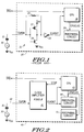
- FIG. 1 illustrates in partial schematic and partial block diagram form an integrated circuit in accordance with the prior art.
- FIG. 2 illustrates in block diagram form an integrated circuit in accordance with the present invention.
- FIG. 3 illustrates in partial schematic and partial logic diagram form the clock amplifier of FIG. 2.
- FIG. 1 illustrates in partial schematic and partial block diagram form an integrated circuit 20 in accordance with the prior art.
- Integrated circuit 20 includes a conventional clock amplifier circuit 21 which receives a clock signal labelled "CLKIN” and provides a buffered clock signal labelled "CLKOUT” to a central processing unit (CPU) 28 and a peripheral circuit 29 in response.
- Clock amplifier circuit 21 includes a P-channel metaloxide-semiconductor (MOS) transistor 22, an N-channel MOS transistor 23, a resistor 24, and an inverter 25.
- Transistor 22 has a source connected to a power supply voltage terminal labelled "V DD ", a gate for receiving signal CLKIN, and a drain.
- V DD power supply voltage terminal
- V DD is a more-positive power supply voltage terminal providing a voltage having a typical value of approximately five volts.
- Transistor 23 has a drain connected to the drain of transistor 22, a gate for receiving signal CLKIN, and a source connected to a power supply voltage terminal labelled "V SS ".
- V SS is a more-negative power supply voltage terminal providing a voltage having a typical value of approximately zero volts.
- Resistor 24 has a first terminal for receiving signal CLKIN, and a second terminal connected to the drains of transistors 22 and 23.
- Inverter 25 has an input terminal connected to the drains of transistors 22 and 23, and an output terminal for providing signal CLKOUT.
- CPU 28 has inputs for receiving an active-low interrupt request signal labelled " IRQ ⁇ " and signal CLKOUT, and an output terminal for providing clock signals labelled "CPUCLKS".
- Peripheral circuit 29 has an input for receiving the CPUCLKS, and is any conventional circuit which uses clocked or sequential logic, such as an input/output peripheral, switched capacitor filter, digital-to-analog converter (DAC) or analog-to-digital converter (ADC) using a sigma delta modulator, or the like.
- CPU 28 executes instructions from memory (not shown), which may be either internal or external to integrated circuit 20. In response to a stop instruction, CPU 28 goes into a low-power or sleep mode, in which power consumption is reduced.
- CPU 28 keeps the CPUCLKS from changing logic state; peripheral circuit 29 goes into a low-power because internal sequential logic circuitry is not being clocked, and thus consumes very little power.
- CPU 28 itself also enters low-power mode, in which an internal clock generator (not shown) is inactivated, thus preventing its own sequential logic from switching.
- CPU 28 exits low-power mode, and again drives CPUCLKS, upon an activation of signal IRQ ⁇ .
- CPU 28 includes combinational logic responsive to signal IRQ ⁇ for this purpose.
- Voltage source 30 has a first terminal, and a second terminal connected to V SS , and provides a one volt peak-to-peak sinusoidal voltage between the first terminal thereof and V SS .
- Capacitor 31 has a first terminal connected to the first terminal of voltage source 30, and a second terminal for providing signal CLKIN.
- voltage source 30 is AC-coupled to clock amplifier 21.
- Transistors 22 and 23 and resistor 24 together set the DC value of CLKIN.
- Resistor 24 is a relatively high-valued resistor.
- Transistors 22 and 23 amplify a small signal, such as 1 volt peak-to-peak. It is desirable to adjust the gain of inverter 21 such that the output levels are within one threshold drop of V DD and V SS , to save power in inverter 25. Inverter 25 then subsequently increases the logic levels to full-supply. For transistors 22 and 23 to provide enough gain, they must be sized to conduct a large current during switching. In addition, transistors 22 and 23 and resistor 24 set the DC voltage at the gates of transistors 22 and 23 to approximately mid-supply; this voltage is approximately the switchpoint of the inverter formed by transistors 22 and 23. Both transistors 22 and 23 are biased near their threshold voltages, and both transistors are always somewhat conductive. Clock amplifier circuit 21 in fact consumes as much power during low-power mode as during normal operation.
- clock amplifier circuit 21 could be disabled during low-power mode.
- the DC value of signal CLKIN tends to drift during low-power mode due to leakage in capacitor 31.
- the DC value may be so high or so low that the 1 volt peak-to-peak AC component of CLKIN is not sufficient to switch the inverter formed by transistors 22 and 23.
- the length of time required to re-charge capacitor 31 to its correct DC value depends on an RC time constant formed by resistor 24 and capacitor 31. Thus, it may take many cycles after the termination of low-power mode before CLKOUT begins to switch, and many more cycles before CLKOUT achieves approximately a fifty percent duty cycle and thus becomes usable, causing a degradation in performance.
- FIG. 2 illustrates in block diagram form an integrated circuit 40 in accordance with the present invention. Elements in common with FIG. 1 retain their previous reference numbers.
- integrated circuit 40 receives sinusoidal clock signal CLKIN provided by oscillator 30 and capacitor 31 to an input node 42, and signal IRQ ⁇ .
- input node 42 is an integrated circuit bonding pad which receives signal CLKIN through a bonding wire and a lead frame (not shown).
- Integrated circuit 40 includes a clock amplifier circuit 41, a CPU 43, and peripheral circuits 44 and 45.
- clock amplifier 41 receives not only signal CLKIN but also a stop signal labelled "STOP" from CPU 43.
- STOP a stop signal labelled "STOP" from CPU 43.
- clock amplifier circuit 41 disables most of its multiple inverter stages so that current consumption is greatly reduced, but keeps one inverter stage active. The result is that integrated circuit 40 reduces power consumption during low-power mode over integrated circuit 20 of FIG. 1 while providing signal CLKOUT immediately after the end of low-power mode.
- CPU 43 has an input for receiving signal CLKOUT from clock amplifier 41, an input for receiving signal IRQ ⁇ , an output for providing signal STOP, and an output port for providing several clock signals labelled "CPUCLKS".
- CPU 43 has an internal clock generator circuit (not shown) which receives signal CLKOUT and provides signals CPUCLKS in response.
- CPUCLKS may be any desirable set of clock signals useful for the operation of CPU 43 and peripheral circuits 44 and 45, such as four non-overlapping clock signals generated from a two-cycle period of signal CLKOUT.
- CPU 43 goes into a low-power or sleep mode, in which power consumption is reduced.
- CPU 43 keeps the CPUCLKS from changing logic state by gating signal CLKOUT by an internal low-power mode signal (not shown).
- CPU 43 exits low-power mode, and again drives CPUCLKS, upon an activation of signal IRQ ⁇ .
- CPU 43 includes combinational logic responsive to signal IRQ ⁇ for this purpose.
- Peripheral circuit 44 is a coder-decoder (codec), including a sigma-delta analog-to-digital converter (ADC) and sigma-delta digital-to-analog converter (DAC), but may be any other conventional clocked peripheral.
- Peripheral 44 receives both signal CLKOUT and CPUCLKS to perform data conversion synchronized to the operation of CPU 43.
- CMOS complementary metal-oxide-semiconductor
- Peripheral circuit 45 is a serial interface port, and operates in response to CPUCLKS but does not receive signal CLKOUT. Peripheral circuit 45 operates with low power when CPU 43 prevents CPUCLKS from switching. Note that the mechanism used to place a CPU or a peripheral in low-power mode varies from application to application, and many other mechanisms besides those shown may be used.
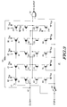
- FIG. 3 illustrates in partial schematic and partial logic diagram form clock amplifier 41 of FIG. 2.
- Clock amplifier 41 includes generally an inverter 50, a switched inverter 51, a constant inverter 52, a resistor 53, and a NAND gate 54.
- Clock amplifier 41 receives signal STOP, and signal CLKIN on input node 42.
- Inverter 50 has an input terminal for receiving signal STOP, and an output terminal.
- Switched inverter 51 has an input terminal connected to node 42 for receiving signal CLKIN thereon, and an output terminal.
- Constant inverter 52 has an input terminal connected to node 42 for receiving signal CLKIN thereon, and an output terminal connected to the output terminal of switched inverter 51.
- Resistor 53 has a first terminal connected to node 42, and a second terminal connected to the output terminals of switched inverter 51 and constant inverter 52.
- NAND gate 54 has a first input terminal connected to the output terminals of switched inverter 51 and constant inverter 52, a second input terminal connected to the output terminal of inverter 50, and an output terminal for providing signal CLKOUT.
- switched inverter 51 includes four switched inverter stages 60, 70, 80, and 90.
- Switched inverter stage 60 includes P-channel transistors 61 and 62, and N-channel transistors 63 and 64.
- Transistor 61 has a source connected to V DD , a gate for receiving signal STOP, and a drain.
- Transistor 62 has a source connected to the drain of transistor 61, a gate connected to node 42 for receiving signal CLKIN, and a drain connected to the first input terminal of NAND gate 54.
- Transistor 63 has a drain connected to the drain of transistor 62, a gate connected to node 42 for receiving signal CLKIN, and a source.
- Transistor 64 has a drain connected to the source of transistor 63, a gate connected to the output terminal of inverter 50, and a source connected to V SS .
- Switched inverter stage 70 includes P-channel transistors 71 and 72, and N-channel transistors 73 and 74.
- Transistor 71 has a source connected to V DD , a gate for receiving signal STOP, and a drain.
- Transistor 72 has a source connected to the drain of transistor 71, a gate connected to node 42 for receiving signal CLKIN, and a drain connected to the first input terminal of NAND gate 54.
- Transistor 73 has a drain connected to the drain of transistor 72, a gate connected to node 42 for receiving signal CLKIN, and a source.
- Transistor 74 has a drain connected to the source of transistor 73, a gate connected to the output terminal of inverter 50, and a source connected to V SS .
- Switched inverter stage 80 includes P-channel transistors 81 and 82, and N-channel transistors 83 and 84.
- Transistor 81 has a source connected to V DD , a gate for receiving signal STOP, and a drain.
- Transistor 82 has a source connected to the drain of transistor 81, a gate connected to node 42 for receiving signal CLKIN, and a drain connected to the first input terminal of NAND gate 54.
- Transistor 83 has a drain connected to the drain of transistor 82, a gate connected to node 42 for receiving signal CLKIN, and a source.
- Transistor 84 has a drain connected to the source of transistor 83, a gate connected to the output terminal of inverter 50, and a source connected to V SS .
- Switched inverter stage 90 includes P-channel transistors 91 and 92, and N-channel transistors 93 and 94.
- Transistor 91 has a source connected to V DD , a gate for receiving signal STOP, and a drain.
- Transistor 92 has a source connected to the drain of transistor 91, a gate connected to node 42 for receiving signal CLKIN, and a drain connected to the first input terminal of NAND gate 54.
- Transistor 93 has a drain connected to the drain of transistor 92, a gate connected to node 42 for receiving signal CLKIN, and a source.
- Transistor 94 has a drain connected to the source of transistor 93, a gate connected to the output terminal of inverter 50, and a source connected to V SS .
- Constant inverter stage 52 includes P-channel transistors 101 and 102, and N-channel transistors 103 and 104.
- Transistor 101 has a source connected to V DD , a gate connected to V SS , and a drain.
- Transistor 102 has a source connected to the drain of transistor 101, a gate connected to node 42 for receiving signal CLKIN, and a drain connected to the first input terminal of NAND gate 54.
- Transistor 103 has a drain connected to the drain of transistor 102, a gate connected to node 42 for receiving signal CLKIN, and a source.
- Transistor 104 has a drain connected to the source of transistor 63, a gate connected to V DD , and a source connected to V SS .
- Switched inverter stages 60, 70, 80, and 90 of clock amplifier 41 are disabled during low-power mode by isolating the sources of inverter switching transistors from their respective power supply potentials. For example, during low-power mode transistor 61 is nonconductive, causing the source of transistor 62 to be isolated from V DD . However, constant inverter 52 is always active, and thus keeps the DC value at node 42 at the switchpoint of switched inverter 51 and constant inverter 52.
- the ratio of the equivalent P-channel gate width-to-gate length (W/L) and the equivalent N-channel W/L in constant inverter 52 is match to the ratio of the equivalent P-channel W/L and the equivalent N-channel W/L of the stages of switched inverter 51.
- the gate size of transistor 101 is matched to the gate sizes of transistors 61, 71, 81, and 91.
- constant inverter 52 is able to keep the same DC level on node 42 during low-power mode as during normal operation.
- the DC value at node 42 (and the switchpoint of switched inverter 51 and constant inverter 52) is set to halfway between V DD and V SS or approximately 2.5 volts.
- Typical values for the components are 80 kilohms for resistor 53; 1 nanofarad for capacitor 31 of FIG. 2; W/L of: 14/4 for transistors 61, 71, 81, 91, and 101; 12/6 for transistors 62, 72, 82, 92, and 102; 5/6 for transistors 63, 73, 83, 93, and 103; and 6/4 for transistors 64, 74, 84, 94, and 104.
- these sizes may vary as design and manufacturing processes vary. It should also be apparent that the number of switched inverter stages will vary in different embodiments; at a minimum, one switched inverter stage and one constant inverter stage are required.
- a clock amplifier according to the present invention may include a switched inverter having more or less than four switched inverter stages.
- the stop signal may be provided from a source external to the integrated circuit rather than by an on-chip CPU. Accordingly, it is intended by the appended claims to cover all modifications of the invention which fall within the true spirit and scope of the invention.
Abstract
Description
- This invention relates generally to electronic circuits, and more particularly, to integrated circuits with a low-power mode and clock amplifier circuits for such integrated circuits.
- Many integrated circuits require an external clock signal to control sequential logic, switched-capacitor filters, or the like. The clock signal must be amplified and buffered on-chip in order to drive a large number of clocked circuits. In some very-large-scale integration (VLSI) devices it is necessary to minimize high-frequency interference caused by harmonics contained in a square wave input clock signal. For these devices, the input clock signal is preferably a sinusoidal signal of relatively small amplitude, such as one volt peak-to-peak, which is alternating current-(AC-) coupled through a capacitor to a clock amplifier. The clock amplifier typically includes an inverter which is self-biased to keep the direct current (DC) voltage on the input node near the switchpoint of the inverter.
- An important feature for integrated circuits is to be able to operate in a low-power or "sleep" mode. In the low-power mode, most circuitry is disabled to save power and this circuitry does not need to be clocked. Upon re-entering normal operation, this circuitry again needs a clock signal for proper operation. It is desirable for the integrated circuit to disable as much circuitry as possible during low-power mode and to recover quickly from low-power mode. These performance requirements create a tradeoff for the clock amplifier. If the clock amplifier is disabled during low-power mode, then the coupling capacitor may discharge and the output of the clock amplifier will not switch while the coupling capacitor is recharging. However, the amplifier is always biased near its switchpoint during operation, resulting in a significant DC current. Thus, if the clock amplifier remains enabled during low-power mode, power consumption increases. A clock amplifier circuit which avoids these tradeoffs is needed.
- Accordingly, there is provided, in one form, an integrated circuit with a low-power mode, comprising an inverter portion, a resistor, a logic portion, and an internal circuit. The inverter portion receives a clock signal and a stop signal, and provides an output signal on an output terminal thereof in response to the clock signal. The inverter portion includes a switched inverter and a constant inverter. The switched inverter receives the clock signal and the stop signal, and provides a first voltage at the output terminal of the inverter portion responsive to the clock signal when the stop signal is inactive. The constant inverter receives the clock signal and provides a second voltage at the output terminal of the inverter responsive to the clock signal and independent of the stop signal. The resistor has a first terminal for receiving the clock signal, and a second terminal coupled to the output terminal of the inverter. The logic portion is coupled to the inverter portion, and provides a clock output signal in response to the output signal of the inverter portion, when the stop signal is inactive. The internal circuit has a clock input terminal for receiving the clock output signal.
- In another form, there is provided a clock amplifier circuit comprising at least one switched inverter stage, an inverter, a resistor, and a logic portion. Each switched inverter stage has an input terminal for receiving a clock signal, a control input terminal for receiving a stop signal, and an output terminal connected to an output node. The inverter has an input terminal for receiving the clock signal, and an output terminal coupled to the output node. The resistor has a first terminal coupled to the input terminals of each switched inverter stage and to the input terminal of the inverter, and a second terminal coupled to the output node. The logic portion is coupled to each switched inverter stage and to the inverter, and provides a clock output signal in response to a voltage on the output node, when the stop signal is inactive.
- These and other features and advantages will be more clearly understood from the following detailed description taken in conjunction with the accompanying drawings.
- FIG. 1 illustrates in partial schematic and partial block diagram form an integrated circuit in accordance with the prior art.
- FIG. 2 illustrates in block diagram form an integrated circuit in accordance with the present invention.
- FIG. 3 illustrates in partial schematic and partial logic diagram form the clock amplifier of FIG. 2.
- FIG. 1 illustrates in partial schematic and partial block diagram form an
integrated circuit 20 in accordance with the prior art.Integrated circuit 20 includes a conventionalclock amplifier circuit 21 which receives a clock signal labelled "CLKIN" and provides a buffered clock signal labelled "CLKOUT" to a central processing unit (CPU) 28 and aperipheral circuit 29 in response.Clock amplifier circuit 21 includes a P-channel metaloxide-semiconductor (MOS)transistor 22, an N-channel MOS transistor 23, aresistor 24, and aninverter 25.Transistor 22 has a source connected to a power supply voltage terminal labelled "VDD", a gate for receiving signal CLKIN, and a drain. VDD is a more-positive power supply voltage terminal providing a voltage having a typical value of approximately five volts.Transistor 23 has a drain connected to the drain oftransistor 22, a gate for receiving signal CLKIN, and a source connected to a power supply voltage terminal labelled "VSS". VSS is a more-negative power supply voltage terminal providing a voltage having a typical value of approximately zero volts.Resistor 24 has a first terminal for receiving signal CLKIN, and a second terminal connected to the drains oftransistors Inverter 25 has an input terminal connected to the drains oftransistors -
CPU 28 has inputs for receiving an active-low interrupt request signal labelled "
Peripheral circuit 29 has an input for receiving the CPUCLKS, and is any conventional circuit which uses clocked or sequential logic, such as an input/output peripheral, switched capacitor filter, digital-to-analog converter (DAC) or analog-to-digital converter (ADC) using a sigma delta modulator, or the like.CPU 28 executes instructions from memory (not shown), which may be either internal or external to integratedcircuit 20. In response to a stop instruction,CPU 28 goes into a low-power or sleep mode, in which power consumption is reduced. In order to reduce power consumption inperipheral circuit 29,CPU 28 keeps the CPUCLKS from changing logic state;peripheral circuit 29 goes into a low-power because internal sequential logic circuitry is not being clocked, and thus consumes very little power.CPU 28 itself also enters low-power mode, in which an internal clock generator (not shown) is inactivated, thus preventing its own sequential logic from switching.CPU 28 exits low-power mode, and again drives CPUCLKS, upon an activation of signal
CPU 28 includes combinational logic responsive to signal
- Also shown in FIG. 1 is a
voltage source 30 and acapacitor 31.Voltage source 30 has a first terminal, and a second terminal connected to VSS, and provides a one volt peak-to-peak sinusoidal voltage between the first terminal thereof and VSS. Capacitor 31 has a first terminal connected to the first terminal ofvoltage source 30, and a second terminal for providing signal CLKIN. Thus,voltage source 30 is AC-coupled toclock amplifier 21.Transistors resistor 24 together set the DC value of CLKIN.Resistor 24 is a relatively high-valued resistor. -
Transistors inverter 21 such that the output levels are within one threshold drop of VDD and VSS, to save power ininverter 25.Inverter 25 then subsequently increases the logic levels to full-supply. Fortransistors transistors resistor 24 set the DC voltage at the gates oftransistors transistors transistors Clock amplifier circuit 21 in fact consumes as much power during low-power mode as during normal operation. - Alternatively,
clock amplifier circuit 21 could be disabled during low-power mode. However, the DC value of signal CLKIN tends to drift during low-power mode due to leakage incapacitor 31. At the end of low-power mode, the DC value may be so high or so low that the 1 volt peak-to-peak AC component of CLKIN is not sufficient to switch the inverter formed bytransistors capacitor 31 to its correct DC value depends on an RC time constant formed byresistor 24 andcapacitor 31. Thus, it may take many cycles after the termination of low-power mode before CLKOUT begins to switch, and many more cycles before CLKOUT achieves approximately a fifty percent duty cycle and thus becomes usable, causing a degradation in performance. - FIG. 2 illustrates in block diagram form an
integrated circuit 40 in accordance with the present invention. Elements in common with FIG. 1 retain their previous reference numbers. As withintegrated circuit 20 of FIG. 1, integratedcircuit 40 receives sinusoidal clock signal CLKIN provided byoscillator 30 andcapacitor 31 to aninput node 42, and signal
input node 42 is an integrated circuit bonding pad which receives signal CLKIN through a bonding wire and a lead frame (not shown). Integratedcircuit 40 includes aclock amplifier circuit 41, aCPU 43, andperipheral circuits - In
integrated circuit 40,clock amplifier 41 receives not only signal CLKIN but also a stop signal labelled "STOP" fromCPU 43. When signal STOP is active,clock amplifier circuit 41 disables most of its multiple inverter stages so that current consumption is greatly reduced, but keeps one inverter stage active. The result is thatintegrated circuit 40 reduces power consumption during low-power mode overintegrated circuit 20 of FIG. 1 while providing signal CLKOUT immediately after the end of low-power mode. -
CPU 43 has an input for receiving signal CLKOUT fromclock amplifier 41, an input for receiving signal
CPU 43 has an internal clock generator circuit (not shown) which receives signal CLKOUT and provides signals CPUCLKS in response. CPUCLKS may be any desirable set of clock signals useful for the operation ofCPU 43 andperipheral circuits CPU 43 goes into a low-power or sleep mode, in which power consumption is reduced. In order to reduce power consumption inperipheral circuits CPU 43 keeps the CPUCLKS from changing logic state by gating signal CLKOUT by an internal low-power mode signal (not shown).CPU 43 exits low-power mode, and again drives CPUCLKS, upon an activation of signal
CPU 43 includes combinational logic responsive to signal
-
Peripheral circuit 44 is a coder-decoder (codec), including a sigma-delta analog-to-digital converter (ADC) and sigma-delta digital-to-analog converter (DAC), but may be any other conventional clocked peripheral. Peripheral 44 receives both signal CLKOUT and CPUCLKS to perform data conversion synchronized to the operation ofCPU 43. During low-power mode, since neither CLKOUT nor CPUCLKS changes logic state, the complementary metal-oxide-semiconductor (CMOS) circuitry inperipheral circuit 44 consumes a minimum of power.Peripheral circuit 45 is a serial interface port, and operates in response to CPUCLKS but does not receive signal CLKOUT.Peripheral circuit 45 operates with low power whenCPU 43 prevents CPUCLKS from switching. Note that the mechanism used to place a CPU or a peripheral in low-power mode varies from application to application, and many other mechanisms besides those shown may be used. - FIG. 3 illustrates in partial schematic and partial logic diagram
form clock amplifier 41 of FIG. 2.Clock amplifier 41 includes generally aninverter 50, a switchedinverter 51, aconstant inverter 52, aresistor 53, and aNAND gate 54.Clock amplifier 41 receives signal STOP, and signal CLKIN oninput node 42.Inverter 50 has an input terminal for receiving signal STOP, and an output terminal. Switchedinverter 51 has an input terminal connected tonode 42 for receiving signal CLKIN thereon, and an output terminal.Constant inverter 52 has an input terminal connected tonode 42 for receiving signal CLKIN thereon, and an output terminal connected to the output terminal of switchedinverter 51.Resistor 53 has a first terminal connected tonode 42, and a second terminal connected to the output terminals of switchedinverter 51 andconstant inverter 52.NAND gate 54 has a first input terminal connected to the output terminals of switchedinverter 51 andconstant inverter 52, a second input terminal connected to the output terminal ofinverter 50, and an output terminal for providing signal CLKOUT. - More specifically, switched
inverter 51 includes four switchedinverter stages inverter stage 60 includes P-channel transistors channel transistors Transistor 61 has a source connected to VDD, a gate for receiving signal STOP, and a drain.Transistor 62 has a source connected to the drain oftransistor 61, a gate connected tonode 42 for receiving signal CLKIN, and a drain connected to the first input terminal ofNAND gate 54.Transistor 63 has a drain connected to the drain oftransistor 62, a gate connected tonode 42 for receiving signal CLKIN, and a source.Transistor 64 has a drain connected to the source oftransistor 63, a gate connected to the output terminal ofinverter 50, and a source connected to VSS. - Switched
inverter stage 70 includes P-channel transistors channel transistors Transistor 71 has a source connected to VDD, a gate for receiving signal STOP, and a drain.Transistor 72 has a source connected to the drain oftransistor 71, a gate connected tonode 42 for receiving signal CLKIN, and a drain connected to the first input terminal ofNAND gate 54.Transistor 73 has a drain connected to the drain oftransistor 72, a gate connected tonode 42 for receiving signal CLKIN, and a source.Transistor 74 has a drain connected to the source oftransistor 73, a gate connected to the output terminal ofinverter 50, and a source connected to VSS. - Switched
inverter stage 80 includes P-channel transistors channel transistors Transistor 81 has a source connected to VDD, a gate for receiving signal STOP, and a drain.Transistor 82 has a source connected to the drain oftransistor 81, a gate connected tonode 42 for receiving signal CLKIN, and a drain connected to the first input terminal ofNAND gate 54.Transistor 83 has a drain connected to the drain oftransistor 82, a gate connected tonode 42 for receiving signal CLKIN, and a source.Transistor 84 has a drain connected to the source oftransistor 83, a gate connected to the output terminal ofinverter 50, and a source connected to VSS. - Switched
inverter stage 90 includes P-channel transistors channel transistors Transistor 91 has a source connected to VDD, a gate for receiving signal STOP, and a drain.Transistor 92 has a source connected to the drain oftransistor 91, a gate connected tonode 42 for receiving signal CLKIN, and a drain connected to the first input terminal ofNAND gate 54.Transistor 93 has a drain connected to the drain oftransistor 92, a gate connected tonode 42 for receiving signal CLKIN, and a source.Transistor 94 has a drain connected to the source oftransistor 93, a gate connected to the output terminal ofinverter 50, and a source connected to VSS. -
Constant inverter stage 52 includes P-channel transistors channel transistors Transistor 101 has a source connected to VDD, a gate connected to VSS, and a drain.Transistor 102 has a source connected to the drain oftransistor 101, a gate connected tonode 42 for receiving signal CLKIN, and a drain connected to the first input terminal ofNAND gate 54.Transistor 103 has a drain connected to the drain oftransistor 102, a gate connected tonode 42 for receiving signal CLKIN, and a source.Transistor 104 has a drain connected to the source oftransistor 63, a gate connected to VDD, and a source connected to VSS. - Switched inverter stages 60, 70, 80, and 90 of
clock amplifier 41 are disabled during low-power mode by isolating the sources of inverter switching transistors from their respective power supply potentials. For example, during low-power mode transistor 61 is nonconductive, causing the source oftransistor 62 to be isolated from VDD. However,constant inverter 52 is always active, and thus keeps the DC value atnode 42 at the switchpoint of switchedinverter 51 andconstant inverter 52. - It is preferable to match the ratio of the equivalent P-channel gate width-to-gate length (W/L) and the equivalent N-channel W/L in
constant inverter 52, to the ratio of the equivalent P-channel W/L and the equivalent N-channel W/L of the stages of switchedinverter 51. For example, the gate size oftransistor 101 is matched to the gate sizes oftransistors constant inverter 52 is able to keep the same DC level onnode 42 during low-power mode as during normal operation. The DC value at node 42 (and the switchpoint of switchedinverter 51 and constant inverter 52) is set to halfway between VDD and VSS or approximately 2.5 volts. Typical values for the components are 80 kilohms forresistor 53; 1 nanofarad forcapacitor 31 of FIG. 2; W/L of: 14/4 fortransistors transistors transistors transistors - While the invention has been described in the context of a preferred embodiment, it will be apparent to those skilled in the art that the present invention may be modified in numerous ways and may assume many embodiments other than that specifically set out and described above. For example, a clock amplifier according to the present invention may include a switched inverter having more or less than four switched inverter stages. Also the stop signal may be provided from a source external to the integrated circuit rather than by an on-chip CPU. Accordingly, it is intended by the appended claims to cover all modifications of the invention which fall within the true spirit and scope of the invention.
Claims (10)
- An integrated circuit with a low-power mode (40), comprising:
inverter means (51, 52) for receiving a clock signal and a stop signal, and for providing an output signal on an output terminal thereof in response to said clock signal, said inverter means (51, 52) including a switched inverter means (51) and a constant inverter means (52);
said switched inverter means (51) for receiving said clock signal and said stop signal, and for providing a first voltage at said output terminal of said inverter means (51, 52) responsive to said clock signal when said stop signal is inactive;
said constant inverter means (52) for receiving said clock signal and for providing a second voltage at said output terminal of said inverter means (51, 52) responsive to said clock signal and independent of said stop signal;
a resistor (53) having a first terminal for receiving said clock signal, and a second terminal coupled to said output terminal of said inverter means (51, 52);
logic means (54) coupled to said inverter means (51, 52), for providing a clock output signal in response to said output signal of said inverter means (51, 52), when said stop signal is inactive; and
an internal circuit (43, 44) having a clock input terminal for receiving said clock output signal. - The integrated circuit (40) of claim 1, wherein said switched inverter means (51) comprises at least one switched inverter stage (60).
- The integrated circuit (40) of claim 1 wherein said constant inverter means (52) comprises:
a fifth transistor (101) having a first current electrode coupled to a first power supply voltage terminal, a control electrode coupled to a second power supply voltage terminal, and a second current electrode;
a sixth transistor (102) having a first current electrode coupled to said second current electrode of said fifth transistor (101), a control electrode for receiving said clock signal, and a second current electrode coupled to said output terminal of said switched inverter means (51);
a seventh transistor (103) having a first current electrode coupled to said second current electrode of said sixth transistor (102), a control electrode for receiving said clock signal, and a second current electrode; and
an eighth transistor (104) having a first current electrode coupled to said second current electrode of said seventh transistor (103), a control electrode coupled to said first power supply voltage terminal, and a second current electrode coupled to said second power supply voltage terminal. - The integrated circuit (40) of claim 1 wherein said internal circuit (43, 44) comprises a central processing unit (28) having an input terminal for receiving said clock signal, and an output terminal for providing said stop signal.
- An integrated circuit with a low-power mode (40), comprising:
at least one switched inverter stage (60) each having an input terminal for receiving a clock signal, a control input terminal for receiving a stop signal, and an output terminal connected to an output node;
an inverter (52) having an input terminal for receiving said clock signal, and an output terminal coupled to said output node;
a resistor (53) having a first terminal coupled to said input terminals of each switched inverter stage (60) and to said input terminal of said inverter (52), and a second terminal coupled to said output node; and
logic means (54) coupled to each switched inverter stage (60) and to said inverter (52), for providing a clock output signal in response to said a voltage on said output node, when said stop signal is inactive; and
an internal circuit (43, 44) having a clock input terminal for receiving said clock output signal. - The integrated circuit (40) of claim 2 or claim 5, wherein each switched inverter stage (60) comprises:
a first transistor (61) having a first current electrode coupled to a first power supply voltage terminal, a control electrode for receiving said stop signal, and a second current electrode;
a second transistor (62) having a first current electrode coupled to said second current electrode of said first transistor (61), a control electrode for receiving said clock signal, and a second current electrode coupled to said output terminal of said at least one switched inverter stage (60);
a third transistor (63) having a first current electrode coupled to said second current electrode of said second transistor (62), a control electrode for receiving said clock signal, and a second current electrode; and
a fourth transistor (64) having a first current electrode coupled to said second current electrode of said third transistor (63), a control electrode for receiving a complement of said stop signal, and a second current electrode coupled to a second power supply voltage terminal. - The integrated circuit (40) of claim 5 wherein said inverter (52) comprises:
a fifth transistor (101) having a first current electrode coupled to a first power supply voltage terminal, a control electrode coupled to a second power supply voltage terminal, and a second current electrode;
a sixth transistor (102) having a first current electrode coupled to said second current electrode of said fifth transistor (101), a control electrode for receiving said clock signal, and a second current electrode coupled to said output terminal of said inverter (52);
a seventh transistor (103) having a first current electrode coupled to said second current electrode of said sixth transistor (102), a control electrode for receiving said clock signal, and a second current electrode; and
an eighth transistor (104) having a first current electrode coupled to said second current electrode of said seventh transistor (103), a control electrode coupled to said first power supply voltage terminal, and a second current electrode coupled to said second power supply voltage terminal. - The integrated circuit (40) of claim 1 or claim 5 wherein said logic means (54) comprises a NAND gate having a first input terminal coupled to said output terminal of said at least one switched inverter stage (60), a second input terminal for receiving a complement of said stop signal, and an output terminal for providing said clock output signal.
- A clock amplifier circuit (41), comprising:
at least one switched inverter stage (60) each having an input terminal for receiving a clock signal, a control input terminal for receiving a stop signal, and an output terminal connected to an output node;
an inverter (52) having an input terminal for receiving said clock signal, and an output terminal coupled to said output node;
a resistor (53) having a first terminal coupled to said input terminals of each switched inverter stage (60) and to said input terminal of said inverter (52), and a second terminal coupled to said output node; and
logic means (54) coupled to each switched inverter stage (60) and to said inverter (52), for providing a clock output signal in response to said a voltage on said output node, when said stop signal is inactive. - The clock amplifier circuit (41) of claim 9, wherein each inverter stage (60) comprises:
a first transistor (61) having a first current electrode coupled to a first power supply voltage terminal, a control electrode for receiving said stop signal, and a second current electrode;
a second transistor (62) having a first current electrode coupled to said second current electrode of said first transistor (61), a control electrode for receiving said clock signal, and a second current electrode coupled to said output terminal of said at least one switched inverter stage (60);
a third transistor (63) having a first current electrode coupled to said second current electrode of said second transistor (62), a control electrode for receiving said clock signal, and a second current electrode; and
a fourth transistor (64) having a first current electrode coupled to said second current electrode of said third transistor (63), a control electrode for receiving a complement of said stop signal, and a second current electrode coupled to a second power supply voltage terminal.
Applications Claiming Priority (2)
| Application Number | Priority Date | Filing Date | Title |
|---|---|---|---|
| US58184 | 1993-05-10 | ||
| US08/058,184 US5430393A (en) | 1993-05-10 | 1993-05-10 | Integrated circuit with a low-power mode and clock amplifier circuit for same |
Publications (2)
| Publication Number | Publication Date |
|---|---|
| EP0624952A2 true EP0624952A2 (en) | 1994-11-17 |
| EP0624952A3 EP0624952A3 (en) | 1995-11-22 |
Family
ID=22015220
Family Applications (1)
| Application Number | Title | Priority Date | Filing Date |
|---|---|---|---|
| EP94303239A Ceased EP0624952A3 (en) | 1993-05-10 | 1994-05-05 | Integrated circuit with a low-power mode and clock amplifier circuit for same. |
Country Status (4)
| Country | Link |
|---|---|
| US (1) | US5430393A (en) |
| EP (1) | EP0624952A3 (en) |
| JP (1) | JPH06348362A (en) |
| KR (1) | KR940027316A (en) |
Cited By (1)
| Publication number | Priority date | Publication date | Assignee | Title |
|---|---|---|---|---|
| US4834735A (en) * | 1986-07-18 | 1989-05-30 | The Proctor & Gamble Company | High density absorbent members having lower density and lower basis weight acquisition zones |
Families Citing this family (19)
| Publication number | Priority date | Publication date | Assignee | Title |
|---|---|---|---|---|
| US6272465B1 (en) | 1994-11-02 | 2001-08-07 | Legerity, Inc. | Monolithic PC audio circuit |
| US5675808A (en) * | 1994-11-02 | 1997-10-07 | Advanced Micro Devices, Inc. | Power control of circuit modules within an integrated circuit |
| US5826068A (en) * | 1994-11-09 | 1998-10-20 | Adaptec, Inc. | Integrated circuit with a serial port having only one pin |
| JPH1013200A (en) * | 1996-06-26 | 1998-01-16 | Mitsubishi Electric Corp | Variable delay circuit |
| US5844435A (en) * | 1997-03-11 | 1998-12-01 | Lucent Technologies Inc | Low power, high accuracy clock circuit and method for integrated circuits |
| US5848014A (en) * | 1997-06-12 | 1998-12-08 | Cypress Semiconductor Corp. | Semiconductor device such as a static random access memory (SRAM) having a low power mode using a clock disable circuit |
| US6052012A (en) * | 1998-06-29 | 2000-04-18 | Cisco Technology, Inc. | Method and apparatus for clock uncertainly minimization |
| US6157222A (en) * | 1999-03-29 | 2000-12-05 | Texas Instruments Incorporated | Low power adjustable input threshold circuit |
| US6425086B1 (en) * | 1999-04-30 | 2002-07-23 | Intel Corporation | Method and apparatus for dynamic power control of a low power processor |
| US6166991A (en) * | 1999-11-03 | 2000-12-26 | Cypress Semiconductor Corp. | Circuit, architecture and method for reducing power consumption in a synchronous integrated circuit |
| US6288593B1 (en) * | 2000-01-04 | 2001-09-11 | Translogic Technology, Inc. | Digital electronic circuit for use in implementing digital logic functions |
| US20090195273A1 (en) * | 2008-02-06 | 2009-08-06 | Micron Technology, Inc. | Start-up circuit for smia input clock buffer |
| JPWO2009147770A1 (en) * | 2008-06-02 | 2011-10-20 | パナソニック株式会社 | Clock signal amplifier circuit |
| US8611379B2 (en) * | 2010-08-20 | 2013-12-17 | Broadcom Corporation | Resonant clock amplifier with a digitally tunable delay |
| US8643418B2 (en) * | 2011-06-02 | 2014-02-04 | Micron Technology, Inc. | Apparatus and methods for altering the timing of a clock signal |
| US8816765B2 (en) * | 2012-08-14 | 2014-08-26 | Broadcom Corporation | Coupled inductor and calibrated complementary low noise amplifiers |
| JP6178096B2 (en) * | 2013-04-03 | 2017-08-09 | 旭化成エレクトロニクス株式会社 | Ring amplifier |
| US9438244B2 (en) * | 2014-10-28 | 2016-09-06 | Xilinx, Inc. | Circuits for and methods of controlling power within an integrated circuit |
| KR102076627B1 (en) * | 2018-08-08 | 2020-02-12 | 서울과학기술대학교 산학협력단 | Neural Recording Analog front end IC |
Citations (4)
| Publication number | Priority date | Publication date | Assignee | Title |
|---|---|---|---|---|
| DE3024936A1 (en) * | 1979-07-13 | 1981-01-29 | Ebauches Electroniques Sa | AC VOLTAGE AMPLIFIER IN THE FORM OF AN INTEGRATED CIRCUIT |
| US4590394A (en) * | 1984-03-13 | 1986-05-20 | Motorola, Inc. | Signal processing circuit with voltage clamped input |
| DE3627681A1 (en) * | 1985-08-14 | 1987-02-26 | Hitachi Ltd | OUTPUT SWITCHING |
| EP0228875A1 (en) * | 1985-12-20 | 1987-07-15 | Nec Corporation | Amplifier circuit having short rise-time |
Family Cites Families (15)
| Publication number | Priority date | Publication date | Assignee | Title |
|---|---|---|---|---|
| US4212083A (en) * | 1976-05-28 | 1980-07-08 | Texas Instruments Incorporated | MOS Integrated with implanted resistor elements |
| JPS5810863B2 (en) * | 1978-04-24 | 1983-02-28 | 株式会社日立製作所 | semiconductor equipment |
| US4758945A (en) * | 1979-08-09 | 1988-07-19 | Motorola, Inc. | Method for reducing power consumed by a static microprocessor |
| US5208489A (en) * | 1986-09-03 | 1993-05-04 | Texas Instruments Incorporated | Multiple compound domino logic circuit |
| US4922141A (en) * | 1986-10-07 | 1990-05-01 | Western Digital Corporation | Phase-locked loop delay line |
| EP0322885A3 (en) * | 1987-12-28 | 1989-08-30 | Kabushiki Kaisha Toshiba | Determination circuit for data coincidence |
| US4890270A (en) * | 1988-04-08 | 1989-12-26 | Sun Microsystems | Method and apparatus for measuring the speed of an integrated circuit device |
| US4899071A (en) * | 1988-08-02 | 1990-02-06 | Standard Microsystems Corporation | Active delay line circuit |
| US4953187A (en) * | 1989-01-23 | 1990-08-28 | Motorola, Inc. | High speed prescaler |
| JPH07114359B2 (en) * | 1989-07-28 | 1995-12-06 | 株式会社東芝 | Semiconductor integrated circuit |
| US5200907A (en) * | 1990-04-16 | 1993-04-06 | Tran Dzung J | Transmission gate logic design method |
| JPH0446707U (en) * | 1990-08-22 | 1992-04-21 | ||
| US5115150A (en) * | 1990-11-19 | 1992-05-19 | Hewlett-Packard Co. | Low power CMOS bus receiver with small setup time |
| US5231319A (en) * | 1991-08-22 | 1993-07-27 | Ncr Corporation | Voltage variable delay circuit |
| US5220216A (en) * | 1992-01-02 | 1993-06-15 | Woo Ann K | Programmable driving power of a CMOS gate |
-
1993
- 1993-05-10 US US08/058,184 patent/US5430393A/en not_active Expired - Fee Related
-
1994
- 1994-04-27 JP JP6110208A patent/JPH06348362A/en active Pending
- 1994-04-28 KR KR1019940009585A patent/KR940027316A/en not_active Application Discontinuation
- 1994-05-05 EP EP94303239A patent/EP0624952A3/en not_active Ceased
Patent Citations (4)
| Publication number | Priority date | Publication date | Assignee | Title |
|---|---|---|---|---|
| DE3024936A1 (en) * | 1979-07-13 | 1981-01-29 | Ebauches Electroniques Sa | AC VOLTAGE AMPLIFIER IN THE FORM OF AN INTEGRATED CIRCUIT |
| US4590394A (en) * | 1984-03-13 | 1986-05-20 | Motorola, Inc. | Signal processing circuit with voltage clamped input |
| DE3627681A1 (en) * | 1985-08-14 | 1987-02-26 | Hitachi Ltd | OUTPUT SWITCHING |
| EP0228875A1 (en) * | 1985-12-20 | 1987-07-15 | Nec Corporation | Amplifier circuit having short rise-time |
Cited By (1)
| Publication number | Priority date | Publication date | Assignee | Title |
|---|---|---|---|---|
| US4834735A (en) * | 1986-07-18 | 1989-05-30 | The Proctor & Gamble Company | High density absorbent members having lower density and lower basis weight acquisition zones |
Also Published As
| Publication number | Publication date |
|---|---|
| US5430393A (en) | 1995-07-04 |
| EP0624952A3 (en) | 1995-11-22 |
| JPH06348362A (en) | 1994-12-22 |
| KR940027316A (en) | 1994-12-10 |
Similar Documents
| Publication | Publication Date | Title |
|---|---|---|
| US5430393A (en) | Integrated circuit with a low-power mode and clock amplifier circuit for same | |
| US5323066A (en) | Method and apparatus for performing power on reset initialization in a data processing system | |
| JPS58215827A (en) | Logical circuit | |
| US3646369A (en) | Multiphase field effect transistor dc driver | |
| US4578601A (en) | High speed TTL clock input buffer circuit which minimizes power and provides CMOS level translation | |
| EP1480341A1 (en) | Semiconductor integrated circuit and its reset method | |
| JPS6468021A (en) | Logic circuit | |
| WO1992009141A1 (en) | Differential output buffer | |
| US20020075038A1 (en) | Active leakage control technique for high performance dynamic circuits | |
| WO1998020609A1 (en) | Low power wake-up system and method | |
| US5917367A (en) | Power supply solution for mixed signal circuits | |
| JP3147955B2 (en) | Semiconductor device | |
| JP3555964B2 (en) | Signal processing circuit and CMOS semiconductor integrated circuit using the same | |
| EP1126362A3 (en) | Microcomputer with internal reset signal generator | |
| JP2546894B2 (en) | Clocked in-phase circuit | |
| KR100331263B1 (en) | Osillator | |
| JP2544796B2 (en) | Input circuit of semiconductor integrated circuit device | |
| JPH1127137A (en) | Semiconductor integrated circuit | |
| JPH0983317A (en) | Short pulse elimination circuit | |
| US5084638A (en) | Driver circuit with controlled output drive signal characteristics | |
| JP2697024B2 (en) | Output circuit | |
| JP3597151B2 (en) | Sound noise mute circuit at power on / off | |
| JPH054846B2 (en) | ||
| JPH04237214A (en) | Clocked inverter | |
| TWI239716B (en) | Power-on-reset circuit with eliminating glitch function |
Legal Events
| Date | Code | Title | Description |
|---|---|---|---|
| PUAI | Public reference made under article 153(3) epc to a published international application that has entered the european phase |
Free format text: ORIGINAL CODE: 0009012 |
|
| AK | Designated contracting states |
Kind code of ref document: A2 Designated state(s): DE FR GB IT |
|
| PUAL | Search report despatched |
Free format text: ORIGINAL CODE: 0009013 |
|
| AK | Designated contracting states |
Kind code of ref document: A3 Designated state(s): DE FR GB IT |
|
| 17P | Request for examination filed |
Effective date: 19960522 |
|
| 17Q | First examination report despatched |
Effective date: 19970624 |
|
| GRAG | Despatch of communication of intention to grant |
Free format text: ORIGINAL CODE: EPIDOS AGRA |
|
| STAA | Information on the status of an ep patent application or granted ep patent |
Free format text: STATUS: THE APPLICATION HAS BEEN REFUSED |
|
| 18R | Application refused |
Effective date: 19991123 |