EP0612622B1 - Ink jet apparatus - Google Patents
Ink jet apparatus Download PDFInfo
- Publication number
- EP0612622B1 EP0612622B1 EP94300974A EP94300974A EP0612622B1 EP 0612622 B1 EP0612622 B1 EP 0612622B1 EP 94300974 A EP94300974 A EP 94300974A EP 94300974 A EP94300974 A EP 94300974A EP 0612622 B1 EP0612622 B1 EP 0612622B1
- Authority
- EP
- European Patent Office
- Prior art keywords
- ink jet
- ink
- jet apparatus
- piezoelectric ceramic
- ratio
- Prior art date
- Legal status (The legal status is an assumption and is not a legal conclusion. Google has not performed a legal analysis and makes no representation as to the accuracy of the status listed.)
- Expired - Lifetime
Links
- 239000000919 ceramic Substances 0.000 claims description 32
- 239000011800 void material Substances 0.000 claims description 10
- 239000013078 crystal Substances 0.000 claims description 9
- 229910010293 ceramic material Inorganic materials 0.000 description 22
- 239000002184 metal Substances 0.000 description 16
- 238000005259 measurement Methods 0.000 description 10
- 238000000034 method Methods 0.000 description 8
- 238000012360 testing method Methods 0.000 description 7
- 230000007246 mechanism Effects 0.000 description 6
- 239000012790 adhesive layer Substances 0.000 description 5
- 230000005684 electric field Effects 0.000 description 5
- 230000010287 polarization Effects 0.000 description 5
- 229920006332 epoxy adhesive Polymers 0.000 description 4
- 239000000463 material Substances 0.000 description 4
- 239000000203 mixture Substances 0.000 description 4
- 238000012545 processing Methods 0.000 description 4
- 230000008569 process Effects 0.000 description 3
- 239000012260 resinous material Substances 0.000 description 3
- 230000007423 decrease Effects 0.000 description 2
- 238000010586 diagram Methods 0.000 description 2
- 239000010410 layer Substances 0.000 description 2
- 238000004519 manufacturing process Methods 0.000 description 2
- 239000000843 powder Substances 0.000 description 2
- 230000003068 static effect Effects 0.000 description 2
- 239000000758 substrate Substances 0.000 description 2
- WAEVWDZKMBQDEJ-UHFFFAOYSA-N 2-[2-(2-methoxypropoxy)propoxy]propan-1-ol Chemical compound COC(C)COC(C)COC(C)CO WAEVWDZKMBQDEJ-UHFFFAOYSA-N 0.000 description 1
- 239000011230 binding agent Substances 0.000 description 1
- 230000008859 change Effects 0.000 description 1
- 230000006835 compression Effects 0.000 description 1
- 238000007906 compression Methods 0.000 description 1
- 239000004020 conductor Substances 0.000 description 1
- 238000010276 construction Methods 0.000 description 1
- 229910003460 diamond Inorganic materials 0.000 description 1
- 239000010432 diamond Substances 0.000 description 1
- 230000000694 effects Effects 0.000 description 1
- 238000009413 insulation Methods 0.000 description 1
- HFGPZNIAWCZYJU-UHFFFAOYSA-N lead zirconate titanate Chemical compound [O-2].[O-2].[O-2].[O-2].[O-2].[Ti+4].[Zr+4].[Pb+2] HFGPZNIAWCZYJU-UHFFFAOYSA-N 0.000 description 1
- 238000012986 modification Methods 0.000 description 1
- 230000004048 modification Effects 0.000 description 1
- 239000000049 pigment Substances 0.000 description 1
- 230000009467 reduction Effects 0.000 description 1
- 238000004544 sputter deposition Methods 0.000 description 1
- 230000000087 stabilizing effect Effects 0.000 description 1
Images


Classifications
-
- B—PERFORMING OPERATIONS; TRANSPORTING
- B41—PRINTING; LINING MACHINES; TYPEWRITERS; STAMPS
- B41J—TYPEWRITERS; SELECTIVE PRINTING MECHANISMS, i.e. MECHANISMS PRINTING OTHERWISE THAN FROM A FORME; CORRECTION OF TYPOGRAPHICAL ERRORS
- B41J2/00—Typewriters or selective printing mechanisms characterised by the printing or marking process for which they are designed
- B41J2/005—Typewriters or selective printing mechanisms characterised by the printing or marking process for which they are designed characterised by bringing liquid or particles selectively into contact with a printing material
- B41J2/01—Ink jet
- B41J2/135—Nozzles
- B41J2/16—Production of nozzles
- B41J2/1621—Manufacturing processes
- B41J2/1623—Manufacturing processes bonding and adhesion
-
- B—PERFORMING OPERATIONS; TRANSPORTING
- B41—PRINTING; LINING MACHINES; TYPEWRITERS; STAMPS
- B41J—TYPEWRITERS; SELECTIVE PRINTING MECHANISMS, i.e. MECHANISMS PRINTING OTHERWISE THAN FROM A FORME; CORRECTION OF TYPOGRAPHICAL ERRORS
- B41J2/00—Typewriters or selective printing mechanisms characterised by the printing or marking process for which they are designed
- B41J2/005—Typewriters or selective printing mechanisms characterised by the printing or marking process for which they are designed characterised by bringing liquid or particles selectively into contact with a printing material
- B41J2/01—Ink jet
- B41J2/135—Nozzles
- B41J2/16—Production of nozzles
- B41J2/1607—Production of print heads with piezoelectric elements
- B41J2/1609—Production of print heads with piezoelectric elements of finger type, chamber walls consisting integrally of piezoelectric material
-
- B—PERFORMING OPERATIONS; TRANSPORTING
- B41—PRINTING; LINING MACHINES; TYPEWRITERS; STAMPS
- B41J—TYPEWRITERS; SELECTIVE PRINTING MECHANISMS, i.e. MECHANISMS PRINTING OTHERWISE THAN FROM A FORME; CORRECTION OF TYPOGRAPHICAL ERRORS
- B41J2/00—Typewriters or selective printing mechanisms characterised by the printing or marking process for which they are designed
- B41J2/005—Typewriters or selective printing mechanisms characterised by the printing or marking process for which they are designed characterised by bringing liquid or particles selectively into contact with a printing material
- B41J2/01—Ink jet
- B41J2/135—Nozzles
- B41J2/16—Production of nozzles
- B41J2/1621—Manufacturing processes
- B41J2/1632—Manufacturing processes machining
- B41J2/1634—Manufacturing processes machining laser machining
-
- B—PERFORMING OPERATIONS; TRANSPORTING
- B41—PRINTING; LINING MACHINES; TYPEWRITERS; STAMPS
- B41J—TYPEWRITERS; SELECTIVE PRINTING MECHANISMS, i.e. MECHANISMS PRINTING OTHERWISE THAN FROM A FORME; CORRECTION OF TYPOGRAPHICAL ERRORS
- B41J2/00—Typewriters or selective printing mechanisms characterised by the printing or marking process for which they are designed
- B41J2/005—Typewriters or selective printing mechanisms characterised by the printing or marking process for which they are designed characterised by bringing liquid or particles selectively into contact with a printing material
- B41J2/01—Ink jet
- B41J2/135—Nozzles
- B41J2/16—Production of nozzles
- B41J2/1621—Manufacturing processes
- B41J2/1637—Manufacturing processes molding
Definitions
- the present invention relates to an ink jet apparatus and, particularly, to a void ratio and an average crystal grain diameter of piezoelectric ceramics.
- Known printer heads include drop-on-demand type ink jet printer heads that utilize piezoelectric ceramics.
- the volume of the ink chambers is varied by the deformation of a piezoelectric ceramic.
- the deformation thereby jets or ejects ink stored in the ink chambers from nozzles as droplets due to a reduction in the volume of the ink chamber.
- the deformation also causes ink to be introduced into the ink chambers from other ink introduction paths due to an increase in the volume.
- ink jet mechanisms are disposed adjacent to each other and droplets of ink are ejected from the ink jet mechanism located at a desired position according to desired print data.
- desired characters and images are formed on a sheet or the like disposed in opposing relationship to the ink jet mechanism.
- FIGs. 7, 8, 9 and 10 of this application are schematic views showing conventional examples, respectively.
- the ink jet apparatus comprises a plurality of side walls 11 and a plurality of ink chambers 12 spaced away from each other in the transverse direction.
- the ink chambers 12 are formed by bonding a piezoelectric ceramic plate 1 subjected to polarization processing in the direction indicated by the arrow 4 to a cover plate 2 composed of a ceramic material or a resinous material or the like with adhesive layers 3 of an epoxy adhesive or the like interposed therebetween.
- Each of the ink chambers 12 has a rectangular cross-section and is shaped in an elongated manner.
- Each of the side walls 11 extends over the overall length of each ink chamber 12.
- Metal electrodes 13 used for application of drive electric fields are formed on both surfaces, each extending from the upper portion adjacent to each adhesive layer 3 of each side wall 11 to the central portion thereof. All of the ink chambers are filled with ink during operation.
- Fig. 8 showing a cross-sectional view of the ink jet apparatus.
- a positive drive voltage is gradually applied to metal electrodes 13e and 13f and metal electrodes 13d and 13g are grounded.
- a drive electric field in the direction indicated by the arrow 14b is exerted on a side wall 11b
- a drive electric field in the direction indicated by the arrow 14c is exerted on a side wall 11c.
- the side walls 11b and 11c are deformed in an outer direction of the ink chamber 12b by a piezoelectric thickness/slip effect.
- the volume of the ink chamber 12b increases due to the deformation, and hence ink pressure decreases.
- the ink is supplied from an ink supply hole 21 (see Fig. 9) to the ink chamber 12b via a manifold 22.
- the application of the drive voltage to the metal electrodes 13e and 13f is abruptly stopped, each of the side walls 11b and 11c is rapidly returned to the original position before their deformation. Therefore, the ink pressure in the ink chamber 12b is abruptly raised and a pressure wave is produced.
- droplets of ink are ejected or jetted from a nozzle 32 that communicates with the ink chamber 12b.
- FIG. 9 is illustrative of a perspective view of the ink jet apparatus.
- a plurality of parallel grooves 12, which form the aforementioned ink chambers, are defined in a piezoelectric ceramic plate 1 subjected to polarization processing by a grinding process using a thin disc-shaped diamond blade.
- the grooves 12 are identical in depth and parallel to each other substantially over the entire region of the piezoelectric ceramic plate 1. However, the grooves 12 gradually become shallow as they reach an end face 15 of the piezoelectric ceramic plate 1 and merge into grooves 16, which are parallel and shallow in the vicinity of the end face 15.
- the metal electrodes 13 are formed on the internal faces of the grooves 12 and 16 respectively by sputtering or the like.
- the metal electrodes 13 are formed only on the upper halves the side faces of the grooves 12.
- the metal electrodes 13 are also formed on side faces and entire bottom faces of the grooves 16 as seen in Fig. 9.
- an ink introduction hole 21 and a manifold 22 are defined in a cover plate 2 made of a ceramic material or a resinous material or the like by grinding or cutting or the like.
- a cover plate 2 made of a ceramic material or a resinous material or the like by grinding or cutting or the like.
- the surface on the groove processed side of the piezoelectric ceramic plate 1 and the surface on the manifold processed side of the cover plate 2 are bonded to each other by epoxy adhesive or the like so that the respective grooves define the ink chambers having the above shapes.
- a nozzle plate 31 having nozzles 32 defined therethrough at positions corresponding to the positions of the ink chambers is bonded to the end faces of the piezoelectric plate 1 and the cover plate 2.
- a substrate 41 having conductive layer patterns 42 formed therein at positions corresponding to the positions of the ink chambers is bonded to the surface of the piezoelectric ceramic plate 1, which is located on the side opposite to the surface on the groove processed side, by epoxy adhesive or the like. Then, the metal electrodes 13 provided on the bottoms of the grooves 16 and the patterns 42 are electrically connected to one another with conductors or lead wires 43 by wire bonding.
- the structure of a controller employed in the conventional example will next be described with reference to Fig. 10 showing a block diagram of the controller.
- the conductive layer patterns 42 formed in the substrate 41 are respectively electrically connected to a corresponding LSI chip 51.
- a clock line 52, a data line 53, a voltage line 54 and a ground line 55 are also electrically connected to the LSI chip 51.
- the LSI chip 51 decides or determines, based on data that appears on the data line 53, from which nozzle the droplets of ink should be jetted or ejected.
- the LSI chip 51 applies a voltage supplied from the voltage line 54 to the patterns 42 electrically connected to the driven metal electrodes in the appropriate ink chambers. Further, the LSI chip 51 applies a voltage of 0 at the ground line 55 to the patterns 42 electrically connected to the metal electrodes in the ink chambers that are not to be activated.
- the relationship between the endurance of the jet and the characteristics of the piezoelectric ceramic material is unclear in the conventional ink jet apparatus described above. Further, the selection of the material is based on the experience of the person in charge of production. Therefore, often the selected piezoelectric ceramic material has poor durability. Hence, the reliability of the ink jet apparatus is low. Further, the ink jet apparatus often has a large variation in drive voltage between the side walls required to stabilize print quality. Thus, the cost of a circuit for stabilizing the print quality increases. Moreover, the drive circuit system is large in structure because of a very high drive voltage, and the cost for taking an insulating measure increases.
- the present invention has been made to solve the aforementioned problems. It is therefore a primary object of the present invention to provide an ink jet apparatus having excellent endurance characteristics and high reliability.
- an ink jet apparatus comprising:
- the ink jet apparatus comprises a plurality of side walls 11 each having a height of preferably 0.4 mm, a width of preferably 0.1 mm and a ratio H/W of the height H of each side wall to the width W thereof.
- a plurality of ink chambers 12 are spaced away from each other in the transverse direction and are formed by bonding a piezoelectric ceramic plate 1 subjected to polarization processing in the direction indicated by the arrow 4 to a cover plate 2 composed of a ceramic material or a resinous material or the like.
- the piezoelectric ceramic plate 1 and cover plate 2 are bonded with adhesive layers 3 formed of epoxy adhesive or the like interposed therebetween.
- Each of the ink chambers 12 has a rectangular cross-section and is shaped in an elongated manner.
- Each of the side walls 11 extends over the overall length of each ink chamber 12.
- Metal electrodes 13 used for application of drive electric fields are formed on both surfaces, each extending from the upper portion adjacent to each adhesive layer 3 of each side wall 11 to the central portion thereof.
- all the ink chambers are filled with pigment ink preferably using TPM (tripropylene glycol methyl ether) as a base.
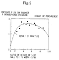
- the ratio H/W of the height of each side wall 11 to the width thereof was set to 4 in the present embodiment.
- an ink jet apparatus having different ratios H/W of height to width of various side walls was experimentally produced.
- the same drive voltage was applied to or across each of the metal electrodes 13, and the pressure P produced within each of the ink chambers 12 was measured.
- the side walls 11 of the produced ink jet apparatus fall within a width W range of 0.04 mm to 0.12 mm and a height H range of 0.1 mm to 0.6 mm.
- the length of each metal electrode 13 is about 1/2 the height of each side wall 11, and a drive voltage to be applied across each metal electrode 13 is 40 V.
- the pressure generated in each ink chamber 12 was measured by the following method.
- a parallel laser beam was radiated into the ink chambers 12 from an upper position of the transparent cover plate 2 via an objective lens of a metal scope.
- a difference in phase between the laser beam reflected from the bottom of each ink chamber 12 and transmitted through the objective lens again and an irradiated laser beam was detected when the laser beam was focused on the bottom of each ink chamber 12.
- the refractive index varies with a change in pressure of the TPM in each ink chamber 12
- the time necessary for the laser beam to pass through each ink chamber 12 varies.
- the pressure in each of the ink chambers 12 can be measured by detecting a variation in the phase difference.
- the result of such a measurement shows that the ratio H/W of the height to the width of each side wall 11 ranges from above 2.5 to below 8 and the pressure in each ink chamber 12 is substantially brought to the maximum as shown in Fig. 2.
- C represents the amount of a static deformation of each side wall 11 at the time of application of the pressure P to the surface of each side wall 11, i.e., the compliance of each side wall 11.
- K represents a constant determined by piezoelectric characteristics and mechanical characteristics of the piezoelectric ceramic plate 1 and compression characteristics of the ink and the like.
- the pressure generated in the ink chambers 12 could be efficiently raised by setting the height-to-width ratio H/W of each of the side walls with the grooves left therebetween to preferably a range from above 2 to below 9. More preferably, a range is set from above 2.5 to below 8. That is, high pressure can be generated in each ink chamber 12 by a low drive voltage and droplets of ink can be ejected or jetted at a velocity or speed and in a volume enough to form characters and images.
- the speed of the ink droplets can be set to a range from 3m/sec to 8m/sec, and the volume can be set to a range from 30pl to 90pl under a low drive-voltage range of 20 to 50V.
- a drive circuit can be simplified and reduced in size, and the ink jet apparatus can be reduced in cost and size over its entirety.
- the height-to-width ratio H/W was set to 4 in the present embodiment.
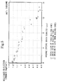
- a sample piezoelectric ceramic plate 1 was manufactured using lead titanate zirconate type piezoelectric ceramics having seven kinds of compositions.
- the ceramic has an average crystal grain diameter and a void ratio of 5 ⁇ m and 3%, respectively, and ratios d 15 /S E44 of piezoelectric constants d 15 to elastic compliances S E44 different from each other.
- Fig. 3 shows the result of measurements of the ratios d 15 /S E44 of the actually-produced seven kinds of piezoelectric ceramic materials. Also shown are the result of measurements of drive voltages required to eject or jet ink at a jet speed of 5m/s free of problems with print quality using a drive circuit similar to that employed in the conventional example shown in Fig. 10.
- the ink jet apparatus was formed by piezoelectric ceramics having such composition that d 15 /S E44 is 10 or above, more preferably, 12 or above in the present embodiment.
- any one of the ink jet apparatus in which the ratio H/W ranges from above 2 to below 9 may preferably use the piezoelectric ceramic material having such composition that d 15 /S E44 is 10 or more. More preferably, d 15 /S E44 12 or more to reduce the drive voltage.
- Print quality is influenced by the piezoelectric ceramic material forming the side walls and the respective ejection or jet mechanisms that differ in jet speed from each other. If the ink jet speed is set to fall within ⁇ 0.5m/s between the respective jet mechanisms, then there is no problem in print quality. When, on the other hand, a variation in the ink jet speed exceeds ⁇ 0.5m/s, the variation in the ink jet speed should be brought into uniformity by respectively adjusting drive voltages applied to the respective jet mechanisms. Therefore, the ink jet velocities at the time the drive voltage was fixed to 60V were measured using the aforementioned seven kinds of piezoelectric ceramic materials whose d 15 /S E44 differ from each other. The result of this measurement is shown in Fig. 4.
- the ink jet apparatus was formed by such a piezoelectric ceramic that the variation in the ratio d 15 /S E44 falls within 4.
- a hot press process was effected on a molded body composed of piezoelectric ceramic powder having a composition at a low temperature of about 1000°C and under a high pressure of 900kg/mm 2 . Further, a ceramic having an average crystal grain diameter of 1 ⁇ m or less was prepared. Thereafter, a subsequent heat-treating temperature and the time interval were varied, and a piezoelectric ceramic material having an average crystal-grain diameter range from below 1 ⁇ m to 15 ⁇ m and a void ratio of 2% or less was obtained.
- the ink jet apparatus is formed having high durability, which is capable of reducing the drive voltage required to eject ink at an ink jet speed of 5m/s to 60V or lower.
- the above apparatus also provides satisfactory print quality and no breaking even if the piezoelectric ceramic material is successively activated a billion times.
Description
wherein said piezoelectric ceramic plate has a piezoelectric constant d15 and an elastic compliance SE44 and characterised in that:
Claims (9)
- An ink jet apparatus comprising:a piezoelectric ceramic plate (1) having spaced side walls (11) therein and electrodes (13) disposed on each side wall (11); anda cover plate (2) coupled to said ceramic plate (1), said cover plate (2) and said side walls (11) defining ink chambers (12), said ink chambers (12) being expandable and contractible upon application of voltage to said electrodes (13);
wherein said piezoelectric ceramic plate (1) has a piezoelectric constant d15 and an elastic compliance SE44 and characterised in that:a ratio of said piezoelectric constant d15 to said elastic compliance SE44 between said side walls (11) varies by not more than 4. - The ink jet apparatus of claim 1, wherein said piezoelectric ceramic plate (1) has a void ratio of 10% or less and has an average crystal grain diameter of 10µm or less.
- The ink jet apparatus of claim 2, wherein said void ratio is 3%.
- The ink jet apparatus of claim 2 or 3, wherein said average crystal grain diameter is 5µm.
- The ink jet apparatus of any preceding claim, wherein said ratio of said piezoelectric constant d15 to said elastic compliance SE44 is 10 or more.
- The ink jet apparatus of claim 5, wherein said ratio of said piezoelectric constant d15 to said elastic compliance SE44 is 12 or more.
- The ink jet apparatus of any preceding claim, wherein said side walls (11) have a height (H) and a width (W) and a height to width ratio in the range of 2 to 9.
- The ink jet apparatus of claim 7, wherein said height to width ratio is in the range of 2.5 to 8.
- The ink jet apparatus of claim 8 wherein said height to width ratio is 4.
Applications Claiming Priority (2)
| Application Number | Priority Date | Filing Date | Title |
|---|---|---|---|
| JP31670/93 | 1993-02-22 | ||
| JP5031670A JPH06238888A (en) | 1993-02-22 | 1993-02-22 | Ink ejector |
Publications (3)
| Publication Number | Publication Date |
|---|---|
| EP0612622A2 EP0612622A2 (en) | 1994-08-31 |
| EP0612622A3 EP0612622A3 (en) | 1995-04-12 |
| EP0612622B1 true EP0612622B1 (en) | 1998-04-15 |
Family
ID=12337568
Family Applications (1)
| Application Number | Title | Priority Date | Filing Date |
|---|---|---|---|
| EP94300974A Expired - Lifetime EP0612622B1 (en) | 1993-02-22 | 1994-02-10 | Ink jet apparatus |
Country Status (4)
| Country | Link |
|---|---|
| US (1) | US5657063A (en) |
| EP (1) | EP0612622B1 (en) |
| JP (1) | JPH06238888A (en) |
| DE (1) | DE69409560T2 (en) |
Families Citing this family (24)
| Publication number | Priority date | Publication date | Assignee | Title |
|---|---|---|---|---|
| US5997135A (en) * | 1995-03-27 | 1999-12-07 | Brother Kogyo Kabushiki Kaisha | Two actuator shear mode type ink jet print head with dimensional relations |
| US5933169A (en) * | 1995-04-06 | 1999-08-03 | Brother Kogyo Kabushiki Kaisha | Two actuator shear mode type ink jet print head with bridging electrode |
| JP2865621B2 (en) * | 1995-06-12 | 1999-03-08 | オセ−ネーデルランド・ビー・ブイ | Inkjet system |
| JP3045180B2 (en) * | 1996-06-04 | 2000-05-29 | シチズン時計株式会社 | Ink jet head and method of manufacturing the same |
| US6808250B2 (en) * | 1997-01-10 | 2004-10-26 | Konica Corporation | Production method of ink-jet head |
| US6139133A (en) * | 1997-03-31 | 2000-10-31 | Brother Kogyo Kabushiki Kaisha | Ink jet head for ejecting ink by exerting pressure on ink in ink channels |
| JPH1178030A (en) * | 1997-09-10 | 1999-03-23 | Brother Ind Ltd | Manufacture of ink jet head |
| JP4582835B2 (en) * | 1999-08-30 | 2010-11-17 | 京セラ株式会社 | Method for manufacturing piezoelectric member for actuator |
| US6755511B1 (en) * | 1999-10-05 | 2004-06-29 | Spectra, Inc. | Piezoelectric ink jet module with seal |
| JP4836307B2 (en) * | 2000-03-31 | 2011-12-14 | 京セラ株式会社 | Piezoelectric ceramic composition and ink jet recording head using the same |
| US6848773B1 (en) | 2000-09-15 | 2005-02-01 | Spectra, Inc. | Piezoelectric ink jet printing module |
| JP4721507B2 (en) * | 2000-11-29 | 2011-07-13 | 京セラ株式会社 | Piezoelectric ceramic composition and ink jet recording head using the same |
| JP4688301B2 (en) * | 2001-01-23 | 2011-05-25 | 京セラ株式会社 | Piezoelectric ceramic composition and ink jet recording head using the same |
| ATE529901T1 (en) * | 2004-02-27 | 2011-11-15 | Canon Kk | PIEZOELECTRIC THIN FILM, METHOD FOR PRODUCING A PIEZOELECTRIC THIN FILM, PIEZOELECTRIC ELEMENT AND INKJET RECORDING HEAD |
| US7281778B2 (en) | 2004-03-15 | 2007-10-16 | Fujifilm Dimatix, Inc. | High frequency droplet ejection device and method |
| US8491076B2 (en) | 2004-03-15 | 2013-07-23 | Fujifilm Dimatix, Inc. | Fluid droplet ejection devices and methods |
| US8708441B2 (en) | 2004-12-30 | 2014-04-29 | Fujifilm Dimatix, Inc. | Ink jet printing |
| JP2007049025A (en) * | 2005-08-11 | 2007-02-22 | Seiko Epson Corp | Actuator, liquid spray head and liquid spraying device |
| US7988247B2 (en) | 2007-01-11 | 2011-08-02 | Fujifilm Dimatix, Inc. | Ejection of drops having variable drop size from an ink jet printer |
| JP4525779B2 (en) * | 2008-03-13 | 2010-08-18 | コニカミノルタホールディングス株式会社 | Inkjet head |
| JP5633200B2 (en) * | 2010-06-08 | 2014-12-03 | 株式会社リコー | Piezoelectric actuator, liquid discharge head, and image forming apparatus |
| JP5578575B2 (en) * | 2010-10-28 | 2014-08-27 | 株式会社村田製作所 | Piezoelectric power generation element and method for estimating power generation amount of piezoelectric power generation element |
| JP6066747B2 (en) | 2012-03-02 | 2017-01-25 | キヤノン株式会社 | Method for manufacturing liquid discharge head and liquid discharge head manufactured by this manufacturing method |
| JP6322369B2 (en) * | 2013-07-18 | 2018-05-09 | エスアイアイ・プリンテック株式会社 | Liquid ejecting head, liquid ejecting apparatus, and method of manufacturing liquid ejecting head |
Citations (1)
| Publication number | Priority date | Publication date | Assignee | Title |
|---|---|---|---|---|
| US4887100A (en) * | 1987-01-10 | 1989-12-12 | Am International, Inc. | Droplet deposition apparatus |
Family Cites Families (11)
| Publication number | Priority date | Publication date | Assignee | Title |
|---|---|---|---|---|
| JPS5768091A (en) * | 1980-10-15 | 1982-04-26 | Hitachi Ltd | Piezoelectric porcelain composition and surface acoustic wave element utilizing it |
| JPS5782165A (en) * | 1980-11-11 | 1982-05-22 | Matsushita Electric Ind Co Ltd | Manufacture of piezoelectric ceramic material |
| JPS57207385A (en) * | 1981-06-16 | 1982-12-20 | Matsushita Electric Ind Co Ltd | Manufacture of composite piezo-electric element |
| JPS62179783A (en) * | 1986-02-04 | 1987-08-06 | Olympus Optical Co Ltd | Piezoelectric actuator |
| GB8824014D0 (en) * | 1988-10-13 | 1988-11-23 | Am Int | High density multi-channel array electrically pulsed droplet deposition apparatus |
| JP2540939B2 (en) * | 1989-04-14 | 1996-10-09 | 富士電機株式会社 | Multilayer piezoelectric actuator element |
| JP3139511B2 (en) * | 1990-11-09 | 2001-03-05 | セイコーエプソン株式会社 | Inkjet recording head |
| JPH04357037A (en) * | 1991-03-19 | 1992-12-10 | Tokyo Electric Co Ltd | Ink jet printer head |
| GB9113023D0 (en) * | 1991-06-17 | 1991-08-07 | Xaar Ltd | Multi-channel arrary droplet deposition apparatus and method of manufacture thereof |
| JPH04369914A (en) * | 1991-06-19 | 1992-12-22 | Matsushita Electric Ind Co Ltd | Piezoelectric ceramic resonator |
| JPH0517216A (en) * | 1991-07-08 | 1993-01-26 | Murata Mfg Co Ltd | Piezoelectric ceramics |
-
1993
- 1993-02-22 JP JP5031670A patent/JPH06238888A/en active Pending
- 1993-11-08 US US08/148,383 patent/US5657063A/en not_active Expired - Lifetime
-
1994
- 1994-02-10 DE DE69409560T patent/DE69409560T2/en not_active Expired - Lifetime
- 1994-02-10 EP EP94300974A patent/EP0612622B1/en not_active Expired - Lifetime
Patent Citations (1)
| Publication number | Priority date | Publication date | Assignee | Title |
|---|---|---|---|---|
| US4887100A (en) * | 1987-01-10 | 1989-12-12 | Am International, Inc. | Droplet deposition apparatus |
Also Published As
| Publication number | Publication date |
|---|---|
| DE69409560D1 (en) | 1998-05-20 |
| EP0612622A3 (en) | 1995-04-12 |
| US5657063A (en) | 1997-08-12 |
| JPH06238888A (en) | 1994-08-30 |
| EP0612622A2 (en) | 1994-08-31 |
| DE69409560T2 (en) | 1998-09-10 |
Similar Documents
| Publication | Publication Date | Title |
|---|---|---|
| EP0612622B1 (en) | Ink jet apparatus | |
| US5265315A (en) | Method of making a thin-film transducer ink jet head | |
| US5860202A (en) | Method for producing a layered piezoelectric element | |
| US6811238B2 (en) | Ink jet recording apparatus, head drive and control device, head drive and control method, and ink jet head | |
| US5508726A (en) | Ink jet apparatus | |
| IL102822A (en) | Method for manufacturing a high density ink jet printhead array | |
| US5421071A (en) | Method of making a piezoelectric liquid-drop ejection device | |
| US5475407A (en) | Ink ejecting printer head | |
| US5502472A (en) | Droplet jet apparatus | |
| US5997135A (en) | Two actuator shear mode type ink jet print head with dimensional relations | |
| JP3185434B2 (en) | Inkjet print head | |
| US5971528A (en) | Piezoelectric ink jet apparatus having nozzles designed for improved jetting | |
| JP3324081B2 (en) | Ink jet device | |
| JPH06238886A (en) | Ink ejector | |
| JPH06198877A (en) | Ink jet printing head and its production | |
| US5917522A (en) | Shearing made ink ejecting apparatus with reliable ejection over a range of temperatures | |
| JPH06226973A (en) | Ink jet apparatus | |
| JPH06226972A (en) | Ink jet apparatus | |
| JPH06226969A (en) | Ink jetting device | |
| JPH08267737A (en) | Ink jet device | |
| JPH06226968A (en) | Ink jetting device | |
| JPH06226970A (en) | Ink jetting device | |
| JPH06226967A (en) | Ink jetting device | |
| JPH08267740A (en) | Ink jet device | |
| JPH08258259A (en) | Ink jet device |
Legal Events
| Date | Code | Title | Description |
|---|---|---|---|
| PUAI | Public reference made under article 153(3) epc to a published international application that has entered the european phase |
Free format text: ORIGINAL CODE: 0009012 |
|
| AK | Designated contracting states |
Kind code of ref document: A2 Designated state(s): DE GB SE |
|
| PUAL | Search report despatched |
Free format text: ORIGINAL CODE: 0009013 |
|
| AK | Designated contracting states |
Kind code of ref document: A3 Designated state(s): DE GB SE |
|
| 17P | Request for examination filed |
Effective date: 19950831 |
|
| 17Q | First examination report despatched |
Effective date: 19960827 |
|
| GRAG | Despatch of communication of intention to grant |
Free format text: ORIGINAL CODE: EPIDOS AGRA |
|
| GRAG | Despatch of communication of intention to grant |
Free format text: ORIGINAL CODE: EPIDOS AGRA |
|
| GRAH | Despatch of communication of intention to grant a patent |
Free format text: ORIGINAL CODE: EPIDOS IGRA |
|
| GRAH | Despatch of communication of intention to grant a patent |
Free format text: ORIGINAL CODE: EPIDOS IGRA |
|
| GRAA | (expected) grant |
Free format text: ORIGINAL CODE: 0009210 |
|
| AK | Designated contracting states |
Kind code of ref document: B1 Designated state(s): DE GB SE |
|
| REF | Corresponds to: |
Ref document number: 69409560 Country of ref document: DE Date of ref document: 19980520 |
|
| PLBQ | Unpublished change to opponent data |
Free format text: ORIGINAL CODE: EPIDOS OPPO |
|
| PLBI | Opposition filed |
Free format text: ORIGINAL CODE: 0009260 |
|
| PLBF | Reply of patent proprietor to notice(s) of opposition |
Free format text: ORIGINAL CODE: EPIDOS OBSO |
|
| 26 | Opposition filed |
Opponent name: XAAR TECHNOLOGY LIMITED Effective date: 19990115 |
|
| PLBF | Reply of patent proprietor to notice(s) of opposition |
Free format text: ORIGINAL CODE: EPIDOS OBSO |
|
| PLBO | Opposition rejected |
Free format text: ORIGINAL CODE: EPIDOS REJO |
|
| PLBN | Opposition rejected |
Free format text: ORIGINAL CODE: 0009273 |
|
| STAA | Information on the status of an ep patent application or granted ep patent |
Free format text: STATUS: OPPOSITION REJECTED |
|
| 27O | Opposition rejected |
Effective date: 20001228 |
|
| REG | Reference to a national code |
Ref country code: GB Ref legal event code: IF02 |
|
| PGFP | Annual fee paid to national office [announced via postgrant information from national office to epo] |
Ref country code: SE Payment date: 20091223 Year of fee payment: 17 |
|
| PGFP | Annual fee paid to national office [announced via postgrant information from national office to epo] |
Ref country code: GB Payment date: 20100107 Year of fee payment: 17 Ref country code: DE Payment date: 20100226 Year of fee payment: 17 |
|
| REG | Reference to a national code |
Ref country code: SE Ref legal event code: EUG |
|
| GBPC | Gb: european patent ceased through non-payment of renewal fee |
Effective date: 20110210 |
|
| REG | Reference to a national code |
Ref country code: DE Ref legal event code: R119 Ref document number: 69409560 Country of ref document: DE Effective date: 20110901 |
|
| PG25 | Lapsed in a contracting state [announced via postgrant information from national office to epo] |
Ref country code: GB Free format text: LAPSE BECAUSE OF NON-PAYMENT OF DUE FEES Effective date: 20110210 |
|
| PG25 | Lapsed in a contracting state [announced via postgrant information from national office to epo] |
Ref country code: SE Free format text: LAPSE BECAUSE OF NON-PAYMENT OF DUE FEES Effective date: 20110211 |
|
| PG25 | Lapsed in a contracting state [announced via postgrant information from national office to epo] |
Ref country code: DE Free format text: LAPSE BECAUSE OF NON-PAYMENT OF DUE FEES Effective date: 20110901 |