EP0607902A2 - Linked electrical connectors - Google Patents
Linked electrical connectors Download PDFInfo
- Publication number
- EP0607902A2 EP0607902A2 EP94100593A EP94100593A EP0607902A2 EP 0607902 A2 EP0607902 A2 EP 0607902A2 EP 94100593 A EP94100593 A EP 94100593A EP 94100593 A EP94100593 A EP 94100593A EP 0607902 A2 EP0607902 A2 EP 0607902A2
- Authority
- EP
- European Patent Office
- Prior art keywords
- carrier
- electrical connectors
- series
- linked
- connectors
- Prior art date
- Legal status (The legal status is an assumption and is not a legal conclusion. Google has not performed a legal analysis and makes no representation as to the accuracy of the status listed.)
- Granted
Links
Images


Classifications
-
- H—ELECTRICITY
- H01—ELECTRIC ELEMENTS
- H01R—ELECTRICALLY-CONDUCTIVE CONNECTIONS; STRUCTURAL ASSOCIATIONS OF A PLURALITY OF MUTUALLY-INSULATED ELECTRICAL CONNECTING ELEMENTS; COUPLING DEVICES; CURRENT COLLECTORS
- H01R13/00—Details of coupling devices of the kinds covered by groups H01R12/70 or H01R24/00 - H01R33/00
- H01R13/02—Contact members
- H01R13/10—Sockets for co-operation with pins or blades
- H01R13/11—Resilient sockets
- H01R13/113—Resilient sockets co-operating with pins or blades having a rectangular transverse section
-
- H—ELECTRICITY
- H01—ELECTRIC ELEMENTS
- H01R—ELECTRICALLY-CONDUCTIVE CONNECTIONS; STRUCTURAL ASSOCIATIONS OF A PLURALITY OF MUTUALLY-INSULATED ELECTRICAL CONNECTING ELEMENTS; COUPLING DEVICES; CURRENT COLLECTORS
- H01R11/00—Individual connecting elements providing two or more spaced connecting locations for conductive members which are, or may be, thereby interconnected, e.g. end pieces for wires or cables supported by the wire or cable and having means for facilitating electrical connection to some other wire, terminal, or conductive member, blocks of binding posts
- H01R11/03—Individual connecting elements providing two or more spaced connecting locations for conductive members which are, or may be, thereby interconnected, e.g. end pieces for wires or cables supported by the wire or cable and having means for facilitating electrical connection to some other wire, terminal, or conductive member, blocks of binding posts characterised by the relationship between the connecting locations
- H01R11/09—Individual connecting elements providing two or more spaced connecting locations for conductive members which are, or may be, thereby interconnected, e.g. end pieces for wires or cables supported by the wire or cable and having means for facilitating electrical connection to some other wire, terminal, or conductive member, blocks of binding posts characterised by the relationship between the connecting locations the connecting locations being identical
-
- H—ELECTRICITY
- H01—ELECTRIC ELEMENTS
- H01H—ELECTRIC SWITCHES; RELAYS; SELECTORS; EMERGENCY PROTECTIVE DEVICES
- H01H85/00—Protective devices in which the current flows through a part of fusible material and this current is interrupted by displacement of the fusible material when this current becomes excessive
- H01H85/02—Details
- H01H85/20—Bases for supporting the fuse; Separate parts thereof
- H01H85/203—Bases for supporting the fuse; Separate parts thereof for fuses with blade type terminals
- H01H85/2035—Bases for supporting the fuse; Separate parts thereof for fuses with blade type terminals for miniature fuses with parallel side contacts
-
- H—ELECTRICITY
- H01—ELECTRIC ELEMENTS
- H01R—ELECTRICALLY-CONDUCTIVE CONNECTIONS; STRUCTURAL ASSOCIATIONS OF A PLURALITY OF MUTUALLY-INSULATED ELECTRICAL CONNECTING ELEMENTS; COUPLING DEVICES; CURRENT COLLECTORS
- H01R43/00—Apparatus or processes specially adapted for manufacturing, assembling, maintaining, or repairing of line connectors or current collectors or for joining electric conductors
- H01R43/16—Apparatus or processes specially adapted for manufacturing, assembling, maintaining, or repairing of line connectors or current collectors or for joining electric conductors for manufacturing contact members, e.g. by punching and by bending
Definitions
- the present invention relates to a linked electrical connector, and specifically to linked electrical connectors used as plural connected electrical connectors in a common power supply circuit connected with fuses and installed in a motor vehicle.
- linked electrical connectors include joint boxes, relay boxes, and fuse boxes.
- plural electrical connectors 1A, 1B and 1C (generally indicated as 1) to which fuses are separately connected are installed in individual terminal sockets 4 in the connector box 3.
- one electrical connector 1A is connected to the power supply via a wire 6, and jumpers 8 are used to short circuit (electrically connect) the one electrical connector 1A with the other electrical connectors 1B, 1C in the same power supply circuit.
- the common carrier 2 of the electrical connectors 1 is conventionally used for the jumpers 8.
- the electrical connectors 1 are stamped from metal plate using a press, and the stamped plate is then bent and shaped to form a connector series in which the individual electrical connectors 1 formed in series at a uniform pitch are connected to a common carrier 2 at the wire crimping ends thereof.
- the carrier 2 is cut appropriately so that the linked electrical connectors can be used in series of two electrical connectors 1A and 1B or three electrical connectors 1A, 1B and 1C according to the circuit design of the connector box 3.
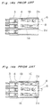
- Figs. 12 and 13 show examples of a series of two linked electrical connectors 1A and 1B connected at the wire crimping end of the electrical connectors 1A and 1B to the carrier 2, which is then cut by a cutter 9.
- a series of three linked electrical connectors is similarly connected at the wire crimping end of the electrical connectors 1A, 1B and 1C to the carrier 2, which is then cut by a cutter 9.
- the cut end of the carrier 2 in both the two and three linked electrical connectors series is a square end with square corners 2a.
- the square corners 2a will tend to catch the inside walls of the connector box 3 when the connectors become biased to the sides, thereby preventing smooth insertion or removal of the connectors.
- an object of the present invention is to provide a linked electrical connector that enables smooth insertion to and removal from the connector box of the linked electrical connector series.
- a linked electrical connector comprises plural electrical connectors formed in series at a uniform pitch on a carrier with the carrier cut at appropriate positions to link plural electrical connectors in series, and is characterized by the cut corners of the carrier being chamfered or curved.
- the cutting operation providing the cut corners of the carrier can be executed during formation of the linked electrical connectors series, or during crimping of the wires to each of the electrical connectors.
- the corners of the cut ends of the carrier are cut using a cutter during the electrical connector carrier cutting process to form a chamfered face or a curved face.
- the chamfered or curved faces of the carrier will not catch the inside wall of the connector box when the carrier becomes biased to said walls during insertion to or removal from the connector box, and these operations can be completed smoothly.
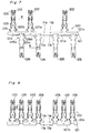
- FIG. 1 A series of three linked electrical connectors 10 according to the first embodiment is shown in Fig. 1.
- a single metal plate is stamped in a press to form the electrical connectors 12A, 12B and 12C in series at a constant pitch along the length of the carrier 11 at the middle of the connectors.
- the opposite sides of the carrier 11 is formed with V-cuts 11a to provide chamfers in a manner described later.
- the carrier is bent between connectors 12A and 12B and between 12B and 12C to reduce the pitch, but the carrier is not bent between the end connectors 12A and 12C of different series, and is therefore left at a greater width W.
- this wide part W of the carrier 11 is placed on the stand 16 during the carrier 11 cutting process, and is cut from above by a cutter 17.
- the shape of the cutter 17 is designed to leave either chamfered or curved faces on the cut corners 11a of the carrier 11.
- the cutting step providing chamfered faces to the carrier 11 corners 11a is executed before the wire crimping step in the embodiment shown in Fig. 1 to form the series of two or three electrical connectors.
- the wire is crimped only to the one electrical connector having the wire barrel 13 and insulation barrel 14 in the series of three or two linked electrical connectors 10, 20.
- the series of three or two linked electrical connectors 10 and 20 is then inserted to the terminal sockets 22 of the connector box 21.
- a carrier 11 in which the corners 11a are curved is particularly effective with connectors of many electrical connectors 12 in series where the carrier 11 is easily deformed, and with connectors connected at the center to the carrier 11 and inserted to or removed from the connector box 21 through a long stroke.
- a linked electrical connector 120 according to a second embodiment is shown.
- a single metal plate is stamped in a press to form first linked electrical connectors 122 on one side 121a (the top in Fig. 1) of a narrow carrier 121, and a second linked electrical connectors 126 on the other side 121b (the bottom in Fig. 1) of the carrier 121.
- a series of four linked electrical connectors and three linked electrical connectors are connected by a common carrier 121.
- the opposite sides of the carrier 11 is formed with V-cuts 11a to provide chamfers in the same manner as that in the first embodiment.
- the first linked electrical connectors 122 are connected to the carrier 121 at the wire crimping end 122a thereof at a constant pitch B along the carrier 121 length.
- a wire barrel 123, insulation barrel 124, and electrical contacts 125 are formed in the normal front of each of the first linked electrical connectors 122 by bending.
- the second linked electrical connectors 126 are similarly connected to the carrier 121 at the wire crimping end 126a thereof at the same constant pitch B along the carrier 121 length.
- the second linked electrical connectors 126 are offset by one-half pitch B to the first linked electrical connectors 122.
- a wire barrel 123, insulation barrel 124, and electrical contacts 125 are also formed in the second linked electrical connectors 126, but are formed on the side opposite that to which they are formed on the first linked electrical connectors 122, as shown in Fig. 11.
- Notches 121c extending to the center of the width of the carrier 121 are also formed on the other side 121b of the carrier 121 on both sides of the base end 126a of each second linked electrical connector 126.
- each of the second linked electrical connectors 126 formed on the other side 121b of the carrier 121 is inverted 180 degrees from the base of the notches 121c (near the center of the carrier 121 width) to the one side 121a.
- the first linked electrical connectors 122 and second linked electrical connectors 126 form a single connector series on the one side 121a of the carrier 121 with the face of each connector facing the same direction as shown in Fig. 8.
- the pitch B' between adjacent first and second linked electrical connectors 122, 126 is one-half pitch B of the stamping, and equal to pitch A of the terminal sockets 22 in the connector box 21.
- the carrier 121 is cut in the above described manner to provide series of four connectors and three connectors.
- the number connectors in one series can be other than four or three, such as two according to the circuit design of the connector box 21.
- the second embodiment it is possible to eliminate the step for bending the carrier in U-shape as required in the first embodiment to reduce the pitch B' of the electrical connectors 122, 126 to half of pitch B.
- the carrier 121 can be simply folded over through part of the carrier 121 width, special shaping dies or processes are unnecessary.
- Carrier 121 strength is also increased because the carrier 121 is doubled in parts.
- the carrier 121 is also more resistant to deformation by external forces, and to compression, stretching, and deflection side-to-side. The dimensional stability of the carrier 121 and linked electrical connector 120 is therefore improved.
- the carrier 121 will not stretch or compress along the length thereof.
- a linked electrical connector 128 according to a third embodiment of the invention is shown in Figs. 9 and 10.
- a rhombus opening 11b is formed at the center of the carrier 121 width, i.e., between the V-cuts 11a at opposite sides to provide chamfers in a similar manner to that in the first embodiment.
- the first and second linked electrical connectors 122, 126 are shaped as in the second embodiment above, but the notches 121c to the center of the carrier 121 width on each side of the second linked electrical connectors 126 ends 126a are not formed.
- the second linked electrical connectors 126 formed on the other side 121b of the carrier 121 are inverted 180 degrees to the one side 121a from the widthwise center of the carrier 121 in the third embodiment. Because the carrier 121 is doubled from the center along the full length thereof in the third embodiment, carrier 121 strength is even greater.
- the other effects and benefits of this design are the same as those of the linked electrical connector 120 according to the second embodiment above.
- the cut corners of the carrier in a linked electrical connector according to the present invention are shaped with a cutter to form chamfered or curved faces during the electrical connector carrier cutting step.
- a linked electrical connector can reduce the pitch between the linked electrical connectors by one-half because the second linked electrical connectors formed on the other side of the carrier are inverted 180 degrees to the first side of the carrier to form a single series of first and second linked electrical connectors on the same side of the carrier.
- the linked electrical connector can be formed by folding the carrier over in two through the carrier width along part or the full length of the carrier, special shaping dies and processes are unnecessary, and the manufacturing cost can be reduced.
Abstract
Description
- The present invention relates to a linked electrical connector, and specifically to linked electrical connectors used as plural connected electrical connectors in a common power supply circuit connected with fuses and installed in a motor vehicle. Common examples of such linked electrical connectors include joint boxes, relay boxes, and fuse boxes.
- In an automotive fuse box as shown in Figs. 14a and 14b, plural
electrical connectors individual terminal sockets 4 in theconnector box 3. In each common power supply circuit, oneelectrical connector 1A is connected to the power supply via awire 6, andjumpers 8 are used to short circuit (electrically connect) the oneelectrical connector 1A with the otherelectrical connectors - As shown in Fig. 12, the
common carrier 2 of theelectrical connectors 1 is conventionally used for thejumpers 8. - The
electrical connectors 1 are stamped from metal plate using a press, and the stamped plate is then bent and shaped to form a connector series in which the individualelectrical connectors 1 formed in series at a uniform pitch are connected to acommon carrier 2 at the wire crimping ends thereof. - The
carrier 2 is cut appropriately so that the linked electrical connectors can be used in series of twoelectrical connectors electrical connectors connector box 3. - Figs. 12 and 13 show examples of a series of two linked
electrical connectors electrical connectors carrier 2, which is then cut by acutter 9. A series of three linked electrical connectors is similarly connected at the wire crimping end of theelectrical connectors carrier 2, which is then cut by acutter 9. - The cut end of the
carrier 2 in both the two and three linked electrical connectors series is a square end withsquare corners 2a. As a result, when inserted to theterminal sockets 4, or removed from theterminal sockets 4, of theconnector box 3 as shown in Figs. 14A and 14B, thesquare corners 2a will tend to catch the inside walls of theconnector box 3 when the connectors become biased to the sides, thereby preventing smooth insertion or removal of the connectors. - As the number of
electrical connectors 1 in a single series increases and a single wire must be held to insert or remove these plural connectors, it becomes even easier for thecarrier 2 to become biased to theconnector box 3 walls, and thesquare corners 2a catch even more easily. - Therefore, an object of the present invention is to provide a linked electrical connector that enables smooth insertion to and removal from the connector box of the linked electrical connector series.
- To achieve this object, a linked electrical connector according to the present invention comprises plural electrical connectors formed in series at a uniform pitch on a carrier with the carrier cut at appropriate positions to link plural electrical connectors in series,
and is characterized by the cut corners of the carrier being chamfered or curved. - The cutting operation providing the cut corners of the carrier can be executed during formation of the linked electrical connectors series, or during crimping of the wires to each of the electrical connectors.
- In a linked electrical connector according to the present invention, the corners of the cut ends of the carrier are cut using a cutter during the electrical connector carrier cutting process to form a chamfered face or a curved face. As a result, the chamfered or curved faces of the carrier will not catch the inside wall of the connector box when the carrier becomes biased to said walls during insertion to or removal from the connector box, and these operations can be completed smoothly.
- The present invention will become more fully understood from the detailed description given below and the accompanying diagrams wherein:
- Fig. 1 is a plan view of a series of three linked electrical connectors according to the first embodiment of the invention,
- Fig. 2 is a front view of the cutting operation for separating the series of linked electrical connectors shown in Fig. 1,
- Fig. 3 an oblique view of the connector box and linked electrical connectors,
- Fig. 4 is a cross section of the connector box,
- Figs. 5a and 5b are oblique views of a series of two linked electrical connectors, and a series of three linked electrical connectors, respectively,
- Figs. 6a and 6b are plan views showing insertion of a series of two linked electrical connectors, and a series of three linked electrical connectors, respectively,
- Figs. 7 and 8 are plan views of a series of four linked electrical connectors and three linked electrical connectors according to the second embodiment of the invention, respectively shown before and after carrier bending,
- Figs. 9 and 10 are plan views of a series of four linked electrical connectors and three linked electrical connectors according to a third embodiment of the invention, respectively shown before and after carrier bending,
- Fig. 11 is a side view of the linked electrical connector of the second and third embodiments before bending,
- Figs. 12 and 13 are plan views of the cutting operation in a conventional series of two linked electrical connectors,
- Figs. 14a and 14b are plan views showing insertion of a series of two linked electrical connectors, and insertion of a series of three linked electrical connectors, respectively.
- The preferred embodiments of the present invention are described below with reference to the accompanying figures.
- A series of three linked
electrical connectors 10 according to the first embodiment is shown in Fig. 1. As shown in Fig. 1, a single metal plate is stamped in a press to form theelectrical connectors carrier 11 at the middle of the connectors. - In this series of three
electrical connectors 12A-12C, awire barrel 13,insulation barrel 14, andelectrical contacts 15 are formed in thecenter connector 12B by bending, andelectrical contacts 15 are formed in theside connectors - Between the two series of three connectors, the opposite sides of the
carrier 11 is formed with V-cuts 11a to provide chamfers in a manner described later. - The carrier is bent between
connectors end connectors - As shown in Fig. 2, this wide part W of the
carrier 11 is placed on thestand 16 during thecarrier 11 cutting process, and is cut from above by acutter 17. - The shape of the
cutter 17 is designed to leave either chamfered or curved faces on thecut corners 11a of thecarrier 11. - As a result, all four
corners 11a on both ends of thecut carrier 11 in this series of three linkedelectrical connectors 10 are chamfered or curved as shown in Fig. 5b. It should also be noted that the fourcorners 11a on both ends of thecut carrier 11 in a series of two linkedelectrical connectors 20 are also chamfered or curved as shown in Fig. 5a. - The cutting step providing chamfered faces to the
carrier 11corners 11a is executed before the wire crimping step in the embodiment shown in Fig. 1 to form the series of two or three electrical connectors. - In addition, the wire is crimped only to the one electrical connector having the
wire barrel 13 andinsulation barrel 14 in the series of three or two linkedelectrical connectors - It should also be noted that it is not necessary to cut the
carrier 11 during the linked electrical connector stamping process, and thecarrier 11 can be cut to provide the chamfered faces during the wire crimping step. - As shown in Figs. 3 and 4, the series of three or two linked
electrical connectors terminal sockets 22 of theconnector box 21. - When the series of two linked
electrical connectors 20 is inserted to or removed from theconnector box 21terminal sockets 22 as shown in Fig. 6a, or when the series of three linkedelectrical connectors 10 inserted to or removed from theconnector box 21terminal sockets 22 as shown in Fig. 6b, the chamfers or curves provided on thecut corners 11a of thecarrier 11 do not catch the inside walls of theconnector box 21 even if thecarrier 11 becomes biased to the walls, and both insertion and removal operations can be completed smoothly. - In addition, a
carrier 11 in which thecorners 11a are curved is particularly effective with connectors of manyelectrical connectors 12 in series where thecarrier 11 is easily deformed, and with connectors connected at the center to thecarrier 11 and inserted to or removed from theconnector box 21 through a long stroke. - Referring to Figs. 7 and 8, a linked
electrical connector 120 according to a second embodiment is shown. As shown in Fig. 7, a single metal plate is stamped in a press to form first linkedelectrical connectors 122 on oneside 121a (the top in Fig. 1) of anarrow carrier 121, and a second linkedelectrical connectors 126 on theother side 121b (the bottom in Fig. 1) of thecarrier 121. A series of four linked electrical connectors and three linked electrical connectors are connected by acommon carrier 121. - Between the two series of four linked connectors and three linked connectors, the opposite sides of the
carrier 11 is formed with V-cuts 11a to provide chamfers in the same manner as that in the first embodiment. - The first linked
electrical connectors 122 are connected to thecarrier 121 at thewire crimping end 122a thereof at a constant pitch B along thecarrier 121 length. Awire barrel 123,insulation barrel 124, andelectrical contacts 125 are formed in the normal front of each of the first linkedelectrical connectors 122 by bending. - The second linked
electrical connectors 126 are similarly connected to thecarrier 121 at thewire crimping end 126a thereof at the same constant pitch B along thecarrier 121 length. The second linkedelectrical connectors 126, however, are offset by one-half pitch B to the first linkedelectrical connectors 122. As with the first linkedelectrical connectors 122, awire barrel 123,insulation barrel 124, andelectrical contacts 125 are also formed in the second linkedelectrical connectors 126, but are formed on the side opposite that to which they are formed on the first linkedelectrical connectors 122, as shown in Fig. 11. -
Notches 121c extending to the center of the width of thecarrier 121 are also formed on theother side 121b of thecarrier 121 on both sides of thebase end 126a of each second linkedelectrical connector 126. - At around the last step of the linked
electrical connector 120 manufacturing process, each of the second linkedelectrical connectors 126 formed on theother side 121b of thecarrier 121 is inverted 180 degrees from the base of thenotches 121c (near the center of thecarrier 121 width) to the oneside 121a. As a result, the first linkedelectrical connectors 122 and second linkedelectrical connectors 126 form a single connector series on the oneside 121a of thecarrier 121 with the face of each connector facing the same direction as shown in Fig. 8. The pitch B' between adjacent first and second linkedelectrical connectors terminal sockets 22 in theconnector box 21. - The
carrier 121 is cut in the above described manner to provide series of four connectors and three connectors. The number connectors in one series can be other than four or three, such as two according to the circuit design of theconnector box 21. - As will be obvious from the above description, according to the second embodiment, it is possible to eliminate the step for bending the carrier in U-shape as required in the first embodiment to reduce the pitch B' of the
electrical connectors carrier 121 can be simply folded over through part of thecarrier 121 width, special shaping dies or processes are unnecessary. -
Carrier 121 strength is also increased because thecarrier 121 is doubled in parts. Thecarrier 121 is also more resistant to deformation by external forces, and to compression, stretching, and deflection side-to-side. The dimensional stability of thecarrier 121 and linkedelectrical connector 120 is therefore improved. - Furthermore, according to the second embodiment, it is also easier to wind the linked
electrical connector 120 to a reel because thecarrier 121 will not stretch or compress along the length thereof. - A linked
electrical connector 128 according to a third embodiment of the invention is shown in Figs. 9 and 10. - In addition to the V-
cuts 11a, arhombus opening 11b is formed at the center of thecarrier 121 width, i.e., between the V-cuts 11a at opposite sides to provide chamfers in a similar manner to that in the first embodiment. - The first and second linked
electrical connectors notches 121c to the center of thecarrier 121 width on each side of the second linkedelectrical connectors 126ends 126a are not formed. - As a result, the second linked
electrical connectors 126 formed on theother side 121b of thecarrier 121 are inverted 180 degrees to the oneside 121a from the widthwise center of thecarrier 121 in the third embodiment. Because thecarrier 121 is doubled from the center along the full length thereof in the third embodiment,carrier 121 strength is even greater. The other effects and benefits of this design are the same as those of the linkedelectrical connector 120 according to the second embodiment above. - As will be obvious from the above description, the cut corners of the carrier in a linked electrical connector according to the present invention are shaped with a cutter to form chamfered or curved faces during the electrical connector carrier cutting step. As a result, these chamfered or curved corners will not catch on the walls of the connector box even if the carrier becomes biased to the walls during insertion or removal, and these operations can be completed smoothly.
- Furthermore, according to the second and third embodiments, a linked electrical connector can reduce the pitch between the linked electrical connectors by one-half because the second linked electrical connectors formed on the other side of the carrier are inverted 180 degrees to the first side of the carrier to form a single series of first and second linked electrical connectors on the same side of the carrier. In addition, because the linked electrical connector can be formed by folding the carrier over in two through the carrier width along part or the full length of the carrier, special shaping dies and processes are unnecessary, and the manufacturing cost can be reduced.
- In addition, strength is improved because the carrier is doubled over, making the carrier more resistant to deformation by external forces, eliminating side-to-side stretching, compression, and deflection, improving dimensional stability, and enabling easier reel winding.
- The invention being thus described, it will be obvious that the same may be varied in many ways. Such variations are not to be regarded as a departure from the spirit and scope of the invention, and all such modifications as would be obvious to one skilled in the art are intended to be included within the scope of the following claims.
Claims (4)
- A linked electrical connector comprising:
a carrier (11) made of electrically conductive material;
electrical connectors (12A-12C; 122, 126) connected at least on one side of said carrier in series at a uniform pitch;
said carrier (11; 121) formed with V-cuts (11a) on opposite sides thereof at each end of said series of electrical connectors whereby cut edges of the carrier at said V-cuts are chamfered. - A linked electrical connector as claimed in Claim 1, wherein said electrical connectors comprising:
first group electrical connectors (122) connected on a first side of said carrier in series at a twice said uniform pitch;
second group electrical connectors (126) connected on a second side of said carrier formed with the tops and bottoms thereof opposite those of the first group electrical connectors, and in series at said twice said uniform pitch but offset said pitch from the first group electrical connectors, whereby when said carrier, at least portions from which said second group electrical connectors are extending, are folded in half widthwise to rotate the second group electrical connectors 180 degrees to the other side of the carrier, the first group electrical connectors and the second group electrical connectors occur alternately at said uniform pitch on said first side of said carrier. - A linked electrical connector as claimed in Claim 1, wherein one connector in said series of connectors is formed with an electrical wire crimping means (13, 14).
- A linked electrical connector as claimed in Claim 1, wherein each connector in said series of connectors is formed with an electrical wire crimping means (123, 124).
Applications Claiming Priority (6)
| Application Number | Priority Date | Filing Date | Title |
|---|---|---|---|
| JP1203/93U | 1993-01-21 | ||
| JP1204/93U | 1993-01-21 | ||
| JP120393U | 1993-01-21 | ||
| JP120493U | 1993-01-21 | ||
| JP120393U JP2568628Y2 (en) | 1993-01-21 | 1993-01-21 | Chained electrical connector |
| JP1993001204U JP2597507Y2 (en) | 1993-01-21 | 1993-01-21 | Chained electrical connector |
Publications (3)
| Publication Number | Publication Date |
|---|---|
| EP0607902A2 true EP0607902A2 (en) | 1994-07-27 |
| EP0607902A3 EP0607902A3 (en) | 1995-11-15 |
| EP0607902B1 EP0607902B1 (en) | 2001-07-25 |
Family
ID=26334386
Family Applications (1)
| Application Number | Title | Priority Date | Filing Date |
|---|---|---|---|
| EP94100593A Expired - Lifetime EP0607902B1 (en) | 1993-01-21 | 1994-01-17 | Linked electrical connectors assembly |
Country Status (3)
| Country | Link |
|---|---|
| US (1) | US5417589A (en) |
| EP (1) | EP0607902B1 (en) |
| DE (1) | DE69427781T2 (en) |
Cited By (3)
| Publication number | Priority date | Publication date | Assignee | Title |
|---|---|---|---|---|
| DE9409725U1 (en) * | 1994-06-16 | 1994-09-01 | Reinshagen Kabelwerk Gmbh | Potential distributors, in particular for motor vehicles |
| EP0736930A1 (en) * | 1995-04-06 | 1996-10-09 | The Whitaker Corporation | Contact having an independently supported inner contact arm |
| US5938485A (en) * | 1996-09-30 | 1999-08-17 | The Whitaker Corporation | Electrical terminal |
Families Citing this family (16)
| Publication number | Priority date | Publication date | Assignee | Title |
|---|---|---|---|---|
| US5490794A (en) * | 1993-11-05 | 1996-02-13 | Sumitomo Wiring Systems, Ltd. | Branch joint box |
| CA2142131A1 (en) * | 1995-02-09 | 1996-08-10 | Benoit Chevarie | Assembly of multi-terminal telecommunications connectors and terminals |
| JP3551103B2 (en) | 1999-10-22 | 2004-08-04 | 住友電装株式会社 | Joint terminal and joint connector |
| JP3638840B2 (en) * | 1999-12-02 | 2005-04-13 | 矢崎総業株式会社 | Connector connection method |
| US6712115B2 (en) * | 2000-04-14 | 2004-03-30 | Ren Judkins | Headrail for double shade |
| FR2826084B1 (en) * | 2001-06-15 | 2003-08-15 | Nexans | UNIVERSAL FLANGE FOR CYLINDRICAL ELEMENT, PARTICULARLY FOR CABLE |
| DE10317276A1 (en) * | 2003-04-11 | 2004-10-21 | E.G.O. Elektrogerätebau GmbH | Arrangement of switching devices |
| US7044805B1 (en) * | 2004-10-22 | 2006-05-16 | Huang-Chou Huang | Pin contact installation assembly for a terminal |
| DE102004053578B4 (en) * | 2004-11-05 | 2008-09-18 | Lisa Dräxlmaier GmbH | Fuse holder for flat fuses |
| DE102004053577B4 (en) * | 2004-11-05 | 2016-09-22 | Lisa Dräxlmaier GmbH | current bridge |
| US20070125688A1 (en) * | 2005-12-06 | 2007-06-07 | Rotex, Inc. | Screening machine, associated screen panel and seal |
| US8261915B2 (en) * | 2005-12-06 | 2012-09-11 | Rotex Global, Llc | Screening machine and associated screen panel |
| US20110036759A1 (en) * | 2005-12-06 | 2011-02-17 | Rotex, Inc. | Screening machine and associated screen panel |
| US20080223761A1 (en) * | 2007-03-14 | 2008-09-18 | Rotex, Inc. | Sealing Mechanism and Associated Sealing Method for Screening Machines |
| US7838848B2 (en) | 2008-10-23 | 2010-11-23 | Hermes Microvision, Inc. | Patterning device holding apparatus and application thereof |
| DE202013103444U1 (en) | 2013-07-31 | 2014-11-04 | Weidmüller Interface GmbH & Co. KG | Contact element for a plug-in arrangement of a particular externally guided bus system |
Citations (3)
| Publication number | Priority date | Publication date | Assignee | Title |
|---|---|---|---|---|
| US4221456A (en) * | 1979-03-01 | 1980-09-09 | Ford Motor Company | Fuse holder for an automotive fuse terminal block |
| GB2123626A (en) * | 1982-07-06 | 1984-02-01 | Lucas Ind Plc | Fuse box assembly |
| EP0339846A2 (en) * | 1988-04-23 | 1989-11-02 | LUCAS INDUSTRIES public limited company | Fuse box |
Family Cites Families (6)
| Publication number | Priority date | Publication date | Assignee | Title |
|---|---|---|---|---|
| US3325769A (en) * | 1964-09-25 | 1967-06-13 | Rogers Corp | Separable electrical circuit assembly |
| US3345599A (en) * | 1964-11-18 | 1967-10-03 | Amp Inc | Cross-connecting board |
| US4072376A (en) * | 1974-12-06 | 1978-02-07 | Amp Incorporated | Socket assemblies |
| CH628484A5 (en) * | 1978-04-21 | 1982-02-26 | Erni & Co Elektro Ind | METHOD AND CONTACT BAR FOR THE PRODUCTION OF GAS-TIGHT CONNECTIONS FOR PRINTED BACKWALL WIRING. |
| US4230387A (en) * | 1979-04-18 | 1980-10-28 | General Staple Company, Inc. | Continuous connector |
| JPS5911425A (en) * | 1982-07-12 | 1984-01-21 | Nec Corp | Bus control circuit for system applying microcomputer |
-
1994
- 1994-01-10 US US08/179,233 patent/US5417589A/en not_active Expired - Lifetime
- 1994-01-17 DE DE69427781T patent/DE69427781T2/en not_active Expired - Lifetime
- 1994-01-17 EP EP94100593A patent/EP0607902B1/en not_active Expired - Lifetime
Patent Citations (3)
| Publication number | Priority date | Publication date | Assignee | Title |
|---|---|---|---|---|
| US4221456A (en) * | 1979-03-01 | 1980-09-09 | Ford Motor Company | Fuse holder for an automotive fuse terminal block |
| GB2123626A (en) * | 1982-07-06 | 1984-02-01 | Lucas Ind Plc | Fuse box assembly |
| EP0339846A2 (en) * | 1988-04-23 | 1989-11-02 | LUCAS INDUSTRIES public limited company | Fuse box |
Cited By (3)
| Publication number | Priority date | Publication date | Assignee | Title |
|---|---|---|---|---|
| DE9409725U1 (en) * | 1994-06-16 | 1994-09-01 | Reinshagen Kabelwerk Gmbh | Potential distributors, in particular for motor vehicles |
| EP0736930A1 (en) * | 1995-04-06 | 1996-10-09 | The Whitaker Corporation | Contact having an independently supported inner contact arm |
| US5938485A (en) * | 1996-09-30 | 1999-08-17 | The Whitaker Corporation | Electrical terminal |
Also Published As
| Publication number | Publication date |
|---|---|
| EP0607902B1 (en) | 2001-07-25 |
| DE69427781D1 (en) | 2001-08-30 |
| DE69427781T2 (en) | 2002-05-08 |
| US5417589A (en) | 1995-05-23 |
| EP0607902A3 (en) | 1995-11-15 |
Similar Documents
| Publication | Publication Date | Title |
|---|---|---|
| US5417589A (en) | Linked electrical connectors | |
| US4261629A (en) | Slotted plate terminal | |
| US4277124A (en) | Connector having wire-in-slot connecting means and crimped strain relief | |
| EP0572874B1 (en) | Dual thickness blade type electrical terminal | |
| EP0352966B1 (en) | Electrical contact member | |
| EP2151891A1 (en) | A terminal fitting and a method of forming it | |
| EP0245292B1 (en) | Electrical terminal | |
| CN100530824C (en) | Electric wire crimp connector | |
| US3742432A (en) | Electrical terminal having folded blade and method of manufacturing same | |
| EP1035616A1 (en) | Flexible printed circuit board crimp terminal and crimping structure for core therewith | |
| US4527857A (en) | Terminal for connecting a wire to a blade type terminal | |
| EP0503578A1 (en) | Shunted electrical connector | |
| EP3582332A1 (en) | Connection terminal and terminal connection structure | |
| EP0795930B1 (en) | High contact force pin-receiving electrical contact | |
| EP0372767B1 (en) | Miniature insulation displacement electrical contact | |
| EP0649186B1 (en) | Conductor crimping electrical terminal | |
| JPH0754721B2 (en) | Electrical connector terminal | |
| US4243286A (en) | Insulation displacement connector | |
| US2811705A (en) | Electrical connector | |
| EP1089387A2 (en) | A modular female electrical terminal | |
| US5554046A (en) | Solderless terminal | |
| US5766045A (en) | Conductor connection terminal unit | |
| US6113417A (en) | Terminal fitting | |
| US6626693B2 (en) | Metal terminal and method of forming metal terminal | |
| US4626061A (en) | Crimp connect terminals |
Legal Events
| Date | Code | Title | Description |
|---|---|---|---|
| PUAI | Public reference made under article 153(3) epc to a published international application that has entered the european phase |
Free format text: ORIGINAL CODE: 0009012 |
|
| AK | Designated contracting states |
Kind code of ref document: A2 Designated state(s): DE GB |
|
| PUAL | Search report despatched |
Free format text: ORIGINAL CODE: 0009013 |
|
| AK | Designated contracting states |
Kind code of ref document: A3 Designated state(s): DE GB |
|
| 17P | Request for examination filed |
Effective date: 19960412 |
|
| 17Q | First examination report despatched |
Effective date: 19990215 |
|
| RTI1 | Title (correction) |
Free format text: LINKED ELECTRICAL CONNECTORS ASSEMBLY |
|
| GRAG | Despatch of communication of intention to grant |
Free format text: ORIGINAL CODE: EPIDOS AGRA |
|
| GRAG | Despatch of communication of intention to grant |
Free format text: ORIGINAL CODE: EPIDOS AGRA |
|
| GRAH | Despatch of communication of intention to grant a patent |
Free format text: ORIGINAL CODE: EPIDOS IGRA |
|
| GRAH | Despatch of communication of intention to grant a patent |
Free format text: ORIGINAL CODE: EPIDOS IGRA |
|
| GRAA | (expected) grant |
Free format text: ORIGINAL CODE: 0009210 |
|
| AK | Designated contracting states |
Kind code of ref document: B1 Designated state(s): DE GB |
|
| REF | Corresponds to: |
Ref document number: 69427781 Country of ref document: DE Date of ref document: 20010830 |
|
| REG | Reference to a national code |
Ref country code: GB Ref legal event code: IF02 |
|
| PLBE | No opposition filed within time limit |
Free format text: ORIGINAL CODE: 0009261 |
|
| STAA | Information on the status of an ep patent application or granted ep patent |
Free format text: STATUS: NO OPPOSITION FILED WITHIN TIME LIMIT |
|
| 26N | No opposition filed | ||
| PGFP | Annual fee paid to national office [announced via postgrant information from national office to epo] |
Ref country code: DE Payment date: 20130109 Year of fee payment: 20 Ref country code: GB Payment date: 20130116 Year of fee payment: 20 |
|
| REG | Reference to a national code |
Ref country code: DE Ref legal event code: R071 Ref document number: 69427781 Country of ref document: DE |
|
| REG | Reference to a national code |
Ref country code: GB Ref legal event code: PE20 Expiry date: 20140116 |
|
| PG25 | Lapsed in a contracting state [announced via postgrant information from national office to epo] |
Ref country code: GB Free format text: LAPSE BECAUSE OF EXPIRATION OF PROTECTION Effective date: 20140116 Ref country code: DE Free format text: LAPSE BECAUSE OF EXPIRATION OF PROTECTION Effective date: 20140118 |