EP0606162B1 - Image display system with pixel mosaic pattern - Google Patents
Image display system with pixel mosaic pattern Download PDFInfo
- Publication number
- EP0606162B1 EP0606162B1 EP94300080A EP94300080A EP0606162B1 EP 0606162 B1 EP0606162 B1 EP 0606162B1 EP 94300080 A EP94300080 A EP 94300080A EP 94300080 A EP94300080 A EP 94300080A EP 0606162 B1 EP0606162 B1 EP 0606162B1
- Authority
- EP
- European Patent Office
- Prior art keywords
- optical path
- image display
- image
- pixels
- display system
- Prior art date
- Legal status (The legal status is an assumption and is not a legal conclusion. Google has not performed a legal analysis and makes no representation as to the accuracy of the status listed.)
- Expired - Lifetime
Links
Images


Classifications
-
- C—CHEMISTRY; METALLURGY
- C03—GLASS; MINERAL OR SLAG WOOL
- C03B—MANUFACTURE, SHAPING, OR SUPPLEMENTARY PROCESSES
- C03B37/00—Manufacture or treatment of flakes, fibres, or filaments from softened glass, minerals, or slags
- C03B37/01—Manufacture of glass fibres or filaments
- C03B37/012—Manufacture of preforms for drawing fibres or filaments
- C03B37/014—Manufacture of preforms for drawing fibres or filaments made entirely or partially by chemical means, e.g. vapour phase deposition of bulk porous glass either by outside vapour deposition [OVD], or by outside vapour phase oxidation [OVPO] or by vapour axial deposition [VAD]
- C03B37/01486—Means for supporting, rotating or translating the preforms being formed, e.g. lathes
-
- G—PHYSICS
- G02—OPTICS
- G02F—OPTICAL DEVICES OR ARRANGEMENTS FOR THE CONTROL OF LIGHT BY MODIFICATION OF THE OPTICAL PROPERTIES OF THE MEDIA OF THE ELEMENTS INVOLVED THEREIN; NON-LINEAR OPTICS; FREQUENCY-CHANGING OF LIGHT; OPTICAL LOGIC ELEMENTS; OPTICAL ANALOGUE/DIGITAL CONVERTERS
- G02F1/00—Devices or arrangements for the control of the intensity, colour, phase, polarisation or direction of light arriving from an independent light source, e.g. switching, gating or modulating; Non-linear optics
- G02F1/01—Devices or arrangements for the control of the intensity, colour, phase, polarisation or direction of light arriving from an independent light source, e.g. switching, gating or modulating; Non-linear optics for the control of the intensity, phase, polarisation or colour
- G02F1/13—Devices or arrangements for the control of the intensity, colour, phase, polarisation or direction of light arriving from an independent light source, e.g. switching, gating or modulating; Non-linear optics for the control of the intensity, phase, polarisation or colour based on liquid crystals, e.g. single liquid crystal display cells
- G02F1/133—Constructional arrangements; Operation of liquid crystal cells; Circuit arrangements
- G02F1/1333—Constructional arrangements; Manufacturing methods
- G02F1/1335—Structural association of cells with optical devices, e.g. polarisers or reflectors
- G02F1/133504—Diffusing, scattering, diffracting elements
-
- G—PHYSICS
- G09—EDUCATION; CRYPTOGRAPHY; DISPLAY; ADVERTISING; SEALS
- G09G—ARRANGEMENTS OR CIRCUITS FOR CONTROL OF INDICATING DEVICES USING STATIC MEANS TO PRESENT VARIABLE INFORMATION
- G09G3/00—Control arrangements or circuits, of interest only in connection with visual indicators other than cathode-ray tubes
- G09G3/001—Control arrangements or circuits, of interest only in connection with visual indicators other than cathode-ray tubes using specific devices not provided for in groups G09G3/02 - G09G3/36, e.g. using an intermediate record carrier such as a film slide; Projection systems; Display of non-alphanumerical information, solely or in combination with alphanumerical information, e.g. digital display on projected diapositive as background
-
- G—PHYSICS
- G09—EDUCATION; CRYPTOGRAPHY; DISPLAY; ADVERTISING; SEALS
- G09G—ARRANGEMENTS OR CIRCUITS FOR CONTROL OF INDICATING DEVICES USING STATIC MEANS TO PRESENT VARIABLE INFORMATION
- G09G3/00—Control arrangements or circuits, of interest only in connection with visual indicators other than cathode-ray tubes
- G09G3/007—Use of pixel shift techniques, e.g. by mechanical shift of the physical pixels or by optical shift of the perceived pixels
-
- G—PHYSICS
- G09—EDUCATION; CRYPTOGRAPHY; DISPLAY; ADVERTISING; SEALS
- G09G—ARRANGEMENTS OR CIRCUITS FOR CONTROL OF INDICATING DEVICES USING STATIC MEANS TO PRESENT VARIABLE INFORMATION
- G09G3/00—Control arrangements or circuits, of interest only in connection with visual indicators other than cathode-ray tubes
- G09G3/20—Control arrangements or circuits, of interest only in connection with visual indicators other than cathode-ray tubes for presentation of an assembly of a number of characters, e.g. a page, by composing the assembly by combination of individual elements arranged in a matrix no fixed position being assigned to or needed to be assigned to the individual characters or partial characters
- G09G3/34—Control arrangements or circuits, of interest only in connection with visual indicators other than cathode-ray tubes for presentation of an assembly of a number of characters, e.g. a page, by composing the assembly by combination of individual elements arranged in a matrix no fixed position being assigned to or needed to be assigned to the individual characters or partial characters by control of light from an independent source
- G09G3/36—Control arrangements or circuits, of interest only in connection with visual indicators other than cathode-ray tubes for presentation of an assembly of a number of characters, e.g. a page, by composing the assembly by combination of individual elements arranged in a matrix no fixed position being assigned to or needed to be assigned to the individual characters or partial characters by control of light from an independent source using liquid crystals
-
- G—PHYSICS
- G09—EDUCATION; CRYPTOGRAPHY; DISPLAY; ADVERTISING; SEALS
- G09G—ARRANGEMENTS OR CIRCUITS FOR CONTROL OF INDICATING DEVICES USING STATIC MEANS TO PRESENT VARIABLE INFORMATION
- G09G5/00—Control arrangements or circuits for visual indicators common to cathode-ray tube indicators and other visual indicators
-
- H—ELECTRICITY
- H04—ELECTRIC COMMUNICATION TECHNIQUE
- H04N—PICTORIAL COMMUNICATION, e.g. TELEVISION
- H04N23/00—Cameras or camera modules comprising electronic image sensors; Control thereof
- H04N23/60—Control of cameras or camera modules
- H04N23/68—Control of cameras or camera modules for stable pick-up of the scene, e.g. compensating for camera body vibrations
- H04N23/682—Vibration or motion blur correction
- H04N23/685—Vibration or motion blur correction performed by mechanical compensation
- H04N23/686—Vibration or motion blur correction performed by mechanical compensation with a variable apex prism
-
- H—ELECTRICITY
- H04—ELECTRIC COMMUNICATION TECHNIQUE
- H04N—PICTORIAL COMMUNICATION, e.g. TELEVISION
- H04N23/00—Cameras or camera modules comprising electronic image sensors; Control thereof
- H04N23/60—Control of cameras or camera modules
- H04N23/68—Control of cameras or camera modules for stable pick-up of the scene, e.g. compensating for camera body vibrations
- H04N23/682—Vibration or motion blur correction
- H04N23/685—Vibration or motion blur correction performed by mechanical compensation
- H04N23/687—Vibration or motion blur correction performed by mechanical compensation by shifting the lens or sensor position
-
- H—ELECTRICITY
- H04—ELECTRIC COMMUNICATION TECHNIQUE
- H04N—PICTORIAL COMMUNICATION, e.g. TELEVISION
- H04N3/00—Scanning details of television systems; Combination thereof with generation of supply voltages
- H04N3/10—Scanning details of television systems; Combination thereof with generation of supply voltages by means not exclusively optical-mechanical
- H04N3/12—Scanning details of television systems; Combination thereof with generation of supply voltages by means not exclusively optical-mechanical by switched stationary formation of lamps, photocells or light relays
- H04N3/127—Scanning details of television systems; Combination thereof with generation of supply voltages by means not exclusively optical-mechanical by switched stationary formation of lamps, photocells or light relays using liquid crystals
-
- H—ELECTRICITY
- H04—ELECTRIC COMMUNICATION TECHNIQUE
- H04N—PICTORIAL COMMUNICATION, e.g. TELEVISION
- H04N5/00—Details of television systems
- H04N5/74—Projection arrangements for image reproduction, e.g. using eidophor
- H04N5/7416—Projection arrangements for image reproduction, e.g. using eidophor involving the use of a spatial light modulator, e.g. a light valve, controlled by a video signal
- H04N5/7441—Projection arrangements for image reproduction, e.g. using eidophor involving the use of a spatial light modulator, e.g. a light valve, controlled by a video signal the modulator being an array of liquid crystal cells
-
- H—ELECTRICITY
- H04—ELECTRIC COMMUNICATION TECHNIQUE
- H04N—PICTORIAL COMMUNICATION, e.g. TELEVISION
- H04N5/00—Details of television systems
- H04N5/76—Television signal recording
- H04N5/765—Interface circuits between an apparatus for recording and another apparatus
- H04N5/77—Interface circuits between an apparatus for recording and another apparatus between a recording apparatus and a television camera
-
- H—ELECTRICITY
- H04—ELECTRIC COMMUNICATION TECHNIQUE
- H04N—PICTORIAL COMMUNICATION, e.g. TELEVISION
- H04N5/00—Details of television systems
- H04N5/76—Television signal recording
- H04N5/91—Television signal processing therefor
- H04N5/92—Transformation of the television signal for recording, e.g. modulation, frequency changing; Inverse transformation for playback
- H04N5/9201—Transformation of the television signal for recording, e.g. modulation, frequency changing; Inverse transformation for playback involving the multiplexing of an additional signal and the video signal
- H04N5/9206—Transformation of the television signal for recording, e.g. modulation, frequency changing; Inverse transformation for playback involving the multiplexing of an additional signal and the video signal the additional signal being a character code signal
-
- H—ELECTRICITY
- H04—ELECTRIC COMMUNICATION TECHNIQUE
- H04N—PICTORIAL COMMUNICATION, e.g. TELEVISION
- H04N9/00—Details of colour television systems
- H04N9/12—Picture reproducers
-
- H—ELECTRICITY
- H04—ELECTRIC COMMUNICATION TECHNIQUE
- H04N—PICTORIAL COMMUNICATION, e.g. TELEVISION
- H04N9/00—Details of colour television systems
- H04N9/12—Picture reproducers
- H04N9/30—Picture reproducers using solid-state colour display devices
-
- G—PHYSICS
- G02—OPTICS
- G02F—OPTICAL DEVICES OR ARRANGEMENTS FOR THE CONTROL OF LIGHT BY MODIFICATION OF THE OPTICAL PROPERTIES OF THE MEDIA OF THE ELEMENTS INVOLVED THEREIN; NON-LINEAR OPTICS; FREQUENCY-CHANGING OF LIGHT; OPTICAL LOGIC ELEMENTS; OPTICAL ANALOGUE/DIGITAL CONVERTERS
- G02F1/00—Devices or arrangements for the control of the intensity, colour, phase, polarisation or direction of light arriving from an independent light source, e.g. switching, gating or modulating; Non-linear optics
- G02F1/01—Devices or arrangements for the control of the intensity, colour, phase, polarisation or direction of light arriving from an independent light source, e.g. switching, gating or modulating; Non-linear optics for the control of the intensity, phase, polarisation or colour
- G02F1/13—Devices or arrangements for the control of the intensity, colour, phase, polarisation or direction of light arriving from an independent light source, e.g. switching, gating or modulating; Non-linear optics for the control of the intensity, phase, polarisation or colour based on liquid crystals, e.g. single liquid crystal display cells
- G02F1/133—Constructional arrangements; Operation of liquid crystal cells; Circuit arrangements
- G02F1/1333—Constructional arrangements; Manufacturing methods
- G02F1/1335—Structural association of cells with optical devices, e.g. polarisers or reflectors
- G02F1/13363—Birefringent elements, e.g. for optical compensation
-
- G—PHYSICS
- G02—OPTICS
- G02F—OPTICAL DEVICES OR ARRANGEMENTS FOR THE CONTROL OF LIGHT BY MODIFICATION OF THE OPTICAL PROPERTIES OF THE MEDIA OF THE ELEMENTS INVOLVED THEREIN; NON-LINEAR OPTICS; FREQUENCY-CHANGING OF LIGHT; OPTICAL LOGIC ELEMENTS; OPTICAL ANALOGUE/DIGITAL CONVERTERS
- G02F1/00—Devices or arrangements for the control of the intensity, colour, phase, polarisation or direction of light arriving from an independent light source, e.g. switching, gating or modulating; Non-linear optics
- G02F1/01—Devices or arrangements for the control of the intensity, colour, phase, polarisation or direction of light arriving from an independent light source, e.g. switching, gating or modulating; Non-linear optics for the control of the intensity, phase, polarisation or colour
- G02F1/13—Devices or arrangements for the control of the intensity, colour, phase, polarisation or direction of light arriving from an independent light source, e.g. switching, gating or modulating; Non-linear optics for the control of the intensity, phase, polarisation or colour based on liquid crystals, e.g. single liquid crystal display cells
- G02F1/133—Constructional arrangements; Operation of liquid crystal cells; Circuit arrangements
- G02F1/1333—Constructional arrangements; Manufacturing methods
- G02F1/1347—Arrangement of liquid crystal layers or cells in which the final condition of one light beam is achieved by the addition of the effects of two or more layers or cells
- G02F1/13471—Arrangement of liquid crystal layers or cells in which the final condition of one light beam is achieved by the addition of the effects of two or more layers or cells in which all the liquid crystal cells or layers remain transparent, e.g. FLC, ECB, DAP, HAN, TN, STN, SBE-LC cells
Definitions
- the color pixel patterns PTA, PTC are switched in alternate fields, i.e., image information VA, VB containing the information of pixel positions of the color pixel patterns PTA, PTC is switched in alternate fields and supplied to the color image display system for displaying an image represented by the image information VA, VB.
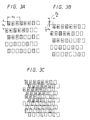
- FIGS. 3A through 3C show the positions of displayed pixels which are optically shifted both vertically and horizontally.
- the color pixel pattern shown in FIG. 3B differs from the color pixel pattern shown in FIG. 2B in that the positions of displayed pixels are optically shifted Pv/2 vertically, and Pc/4 horizontally.
- a color pixel pattern comprises a three-dimensional matrix of pixels arranged in horizontal rows and vertical columns and combined with stripe filters of three primaries of red (R), green (G), and blue (B).
- An optical path that is directed from the color pixel pattern toward the viewer is shifted Pv/2 vertically and Pc/2 horizontally.
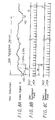
- the sources of the thin-film transistors 11T of each vertical column of pixels are connected in common to each other.
- the sources of the thin-film transistors 11T of the vertical columns of pixels are connected respectively to column lines X1, X2, X3, ⁇ Xi, ⁇ Xm.
- the column lines X1, X2, ⁇ Xi, ⁇ Xm are connected respectively to signal switches 14H1, 14H2, ⁇ 14Hi, ⁇ 14Hm.
- Those signal switches which are connected to the column lines coupled to the pixel columns of green G are supplied with a green primary signal SG.
- Those signal switches which are connected to the column lines coupled to the pixel columns of blue B are supplied with a blue primary signal SB.
- Those signal switches which are connected to the column lines coupled to the pixel columns of red R are supplied with a red primary signal SR.
- the optical path changer 500 makes one revolution in seven frame in synchronism with vertical scanning.
Description
Claims (10)
- A method of increasing resolution of an image displayed to a viewer (1) on an image display system (10) having a matrix of pixels arranged in horizontal rows and vertical columns and selectively energizable to display an image composed of a plurality of pixel patterns in alternate fields, comprising the steps of:providing an optical path changer (30;50) formed of a light refractive member;positioning the optical path changer (30;50) between the image display system (10) and the viewer (1) so that the viewer views the image through the optical path changer which is for shifting the optical path between the display system and the viewer to optically shift a pixel pattern;operating said optical path changer (30;50) to shift said optical path by refraction characterised bydisplaying the pixel pattern on said image display system (10) to be shifted in every field in synchronism with the shifting of said optical path by said optical path changer by shifting a horizontal clock signal of said image display out of phase with a horizontal synchronizing signal of image information supplied thereto in conformity with sampled positions on the displayed image when the optical path is shifted horizontally, andshifting a vertical clock signal of said image display system out of phase with a vertical synchronizing signal of image information supplied thereto in conformity with sampled positions on the displayed image when the optical path is shifted vertically.
- A method according to claim 1, wherein said step of operating the optical path changer comprises the step of moving said light refractive member (50) into and out of said optical path thereby shifting the optical path.
- A method according to claim 1, wherein said light refractive member includes regions having different refractive indices, and said step of operating the optical path changer comprises the step of moving one of said regions into said optical path in alternate fields thereby shifting the optical path.
- A method according to claim 1, wherein said optical path changer comprises an active prism (100) for passing light from said image display system (10) therethrough, said step of operating the optical path changer comprising the step of actuating said active prism in every field thereby shifting the optical path.
- A method according to any one of the preceding claims wherein said pixels are capable of continuously displaying the image until a next portion of image information of which a next field is composed is supplied to the pixels; andproviding an optical path changer;positioning the optical path changer between an image display system and the viewer for selectively shifting an optical path between the image display system and the viewer depending on the field, said shifting beingsaid optical path changer is operated to shift said optical path in synchronism with vertical scanning of said image display system.
- A method according to any one of the preceding claims, wherein said optical path is shifted in one direction by ½ of the pitch of the pixels and in a transverse direction by ¼ of the pitch of pixels of the same color.
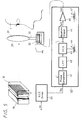
- An image display system comprising:an image display device (10) receiving image information (VI) and having a matrix of pixels (R,G,B) arranged in horizontal rows and vertical columns and selectively energizable in response to a horizontal clock signal and a vertical clock signal to display an image composed of a plurality of pixel patterns in alternate fields;an optical path changer (30;50) formed of a light refractive member disposed between said image display device (10) and a viewer (1) so that the viewer views a displayed image on said image display device through the optical path changer and for shifting the optical path between said image display device and the viewer and to optically shift pixel patterns characterised byshifting means (24) for shifting pixel patterns displayed on said image display device in time relation to the change of the optical path by said optical path changer by shifting said horizontal clock signal in every field out of phase with a horizontal synchronizing signal of the image information supplied to said image display device in conformity with sampled positions on the displayed image when the optical path is shifted horizontally by said optical path changer and/or shifting said vertical clock signal in every field out of phase with a vertical synchronizing signal of the image information in conformity with sampled positions on the displayed image when the optical path is shifted vertically by said optical path changer.
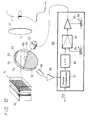
- An image display system according to claim 7, wherein said optical path changer (50;500) comprises a circular member (52) having a rotatable shaft located at a central axis thereof and including circumferentially alternate regions (51, 54; 511-517, 540) for deflecting the optical path by respective different quantities, said circular member being disposed in the optical bath between said image display device and the viewer, whereby said rotatable shaft is rotated in synchronism with vertical scanning of said image display device (10) to cause said circumferentially alternate regions of the circular member to move alternately into said optical path while each field of image information is supplied to said image display device.
- An image display system according to claim 7, wherein said optical path changer comprises a polarization plane rotator (71) and a birefringent plate (72), said polarization plane rotator and said birefringent plate being arranged between said image display device (10) and the viewer (1) such that light from said image display device passes successively through said polarization plane rotator (71) and said birefringent plate (72) in the order named.
- An image display system according to claim 7, 8 or 9, wherein said image display device comprises:horizontal scanning means (16) for successively scanning the horizontal rows of pixels with the horizontal clock signal (HCK);vertical scanning means (13) for successively scanning the vertical columns of pixels with the vertical clock signal (VCK);generating means (24) for generating said horizontal clock signal; andgenerating means (24) for generating said vertical clock signal.
Applications Claiming Priority (4)
| Application Number | Priority Date | Filing Date | Title |
|---|---|---|---|
| JP16955/93 | 1993-01-07 | ||
| JP1695593 | 1993-01-07 | ||
| JP19697393A JP3547015B2 (en) | 1993-01-07 | 1993-07-14 | Image display device and method for improving resolution of image display device |
| JP196973/93 | 1993-07-14 |
Publications (3)
| Publication Number | Publication Date |
|---|---|
| EP0606162A2 EP0606162A2 (en) | 1994-07-13 |
| EP0606162A3 EP0606162A3 (en) | 1994-11-02 |
| EP0606162B1 true EP0606162B1 (en) | 1998-11-11 |
Family
ID=26353409
Family Applications (1)
| Application Number | Title | Priority Date | Filing Date |
|---|---|---|---|
| EP94300080A Expired - Lifetime EP0606162B1 (en) | 1993-01-07 | 1994-01-06 | Image display system with pixel mosaic pattern |
Country Status (4)
| Country | Link |
|---|---|
| US (1) | US5689283A (en) |
| EP (1) | EP0606162B1 (en) |
| JP (1) | JP3547015B2 (en) |
| DE (1) | DE69414427T2 (en) |
Cited By (7)
| Publication number | Priority date | Publication date | Assignee | Title |
|---|---|---|---|---|
| US7853094B2 (en) | 2006-01-24 | 2010-12-14 | Sharp Laboratories Of America, Inc. | Color enhancement technique using skin color detection |
| DE112005002615B4 (en) * | 2004-10-20 | 2010-12-30 | Hewlett-Packard Development Co., L.P., Houston | Pixel Farbwobulation |
| US7898519B2 (en) | 2005-02-17 | 2011-03-01 | Sharp Laboratories Of America, Inc. | Method for overdriving a backlit display |
| US8050512B2 (en) | 2004-11-16 | 2011-11-01 | Sharp Laboratories Of America, Inc. | High dynamic range images from low dynamic range images |
| US8050511B2 (en) | 2004-11-16 | 2011-11-01 | Sharp Laboratories Of America, Inc. | High dynamic range images from low dynamic range images |
| US8121401B2 (en) | 2006-01-24 | 2012-02-21 | Sharp Labortories of America, Inc. | Method for reducing enhancement of artifacts and noise in image color enhancement |
| US8941580B2 (en) | 2006-11-30 | 2015-01-27 | Sharp Laboratories Of America, Inc. | Liquid crystal display with area adaptive backlight |
Families Citing this family (186)
| Publication number | Priority date | Publication date | Assignee | Title |
|---|---|---|---|---|
| JPH10512684A (en) * | 1994-10-25 | 1998-12-02 | ジェームズ エル ファーガソン | Optical display system and method, active and passive dithering using birefringence, color image superposition, and display enhancement |
| US6184969B1 (en) | 1994-10-25 | 2001-02-06 | James L. Fergason | Optical display system and method, active and passive dithering using birefringence, color image superpositioning and display enhancement |
| US6243055B1 (en) | 1994-10-25 | 2001-06-05 | James L. Fergason | Optical display system and method with optical shifting of pixel position including conversion of pixel layout to form delta to stripe pattern by time base multiplexing |
| US5644432A (en) * | 1995-01-17 | 1997-07-01 | Ibm Corporation | Three prism color separator |
| JPH08194207A (en) * | 1995-01-20 | 1996-07-30 | Olympus Optical Co Ltd | Image display device |
| US6061103A (en) * | 1995-01-20 | 2000-05-09 | Olympus Optical Co., Ltd. | Image display apparatus |
| JPH09152572A (en) * | 1995-06-30 | 1997-06-10 | Victor Co Of Japan Ltd | Image processor, image display device, and image pickup device |
| GB9605056D0 (en) * | 1996-03-09 | 1996-05-08 | Philips Electronics Nv | Interlaced image projection apparatus |
| JPH09322099A (en) * | 1996-05-30 | 1997-12-12 | Olympus Optical Co Ltd | Video display device |
| US6559825B2 (en) | 1996-10-31 | 2003-05-06 | Kopin Corporation | Display system for wireless pager |
| US6545654B2 (en) | 1996-10-31 | 2003-04-08 | Kopin Corporation | Microdisplay for portable communication systems |
| US6486862B1 (en) * | 1996-10-31 | 2002-11-26 | Kopin Corporation | Card reader display system |
| US6677936B2 (en) | 1996-10-31 | 2004-01-13 | Kopin Corporation | Color display system for a camera |
| JPH10186313A (en) * | 1996-12-25 | 1998-07-14 | Furontetsuku:Kk | Color liquid crystal display device |
| JP3560756B2 (en) * | 1997-02-13 | 2004-09-02 | アルプス電気株式会社 | Driving method of display device |
| US5815303A (en) * | 1997-06-26 | 1998-09-29 | Xerox Corporation | Fault tolerant projective display having redundant light modulators |
| KR19990009016A (en) * | 1997-07-07 | 1999-02-05 | 윤종용 | Laser projection imaging device and method using birefringent material |
| US6104375A (en) * | 1997-11-07 | 2000-08-15 | Datascope Investment Corp. | Method and device for enhancing the resolution of color flat panel displays and cathode ray tube displays |
| WO1999025161A2 (en) * | 1997-11-11 | 1999-05-20 | Anatoly Ivanov | Methods and devices for picking up/displaying images |
| JP3926922B2 (en) * | 1998-03-23 | 2007-06-06 | オリンパス株式会社 | Image display device |
| JP3963564B2 (en) * | 1998-04-13 | 2007-08-22 | オリンパス株式会社 | Image display device |
| JP3934250B2 (en) | 1998-05-11 | 2007-06-20 | オリンパス株式会社 | Image display device |
| JP4101943B2 (en) | 1998-08-07 | 2008-06-18 | オリンパス株式会社 | Image display device |
| US6307566B1 (en) | 1998-10-07 | 2001-10-23 | Microsoft Corporation | Methods and apparatus for performing image rendering and rasterization operations |
| US6356278B1 (en) | 1998-10-07 | 2002-03-12 | Microsoft Corporation | Methods and systems for asymmeteric supersampling rasterization of image data |
| US6278434B1 (en) | 1998-10-07 | 2001-08-21 | Microsoft Corporation | Non-square scaling of image data to be mapped to pixel sub-components |
| US6236390B1 (en) | 1998-10-07 | 2001-05-22 | Microsoft Corporation | Methods and apparatus for positioning displayed characters |
| US6188385B1 (en) | 1998-10-07 | 2001-02-13 | Microsoft Corporation | Method and apparatus for displaying images such as text |
| JP5231697B2 (en) * | 1998-10-07 | 2013-07-10 | マイクロソフト コーポレーション | Method and computer system for improving the resolution of displayed images |
| US6225973B1 (en) | 1998-10-07 | 2001-05-01 | Microsoft Corporation | Mapping samples of foreground/background color image data to pixel sub-components |
| US6597360B1 (en) * | 1998-10-07 | 2003-07-22 | Microsoft Corporation | Automatic optimization of the position of stems of text characters |
| JP4101954B2 (en) * | 1998-11-12 | 2008-06-18 | オリンパス株式会社 | Image display device |
| JP4103216B2 (en) * | 1998-12-09 | 2008-06-18 | ノーリツ鋼機株式会社 | Photo printing device |
| US6393145B2 (en) | 1999-01-12 | 2002-05-21 | Microsoft Corporation | Methods apparatus and data structures for enhancing the resolution of images to be rendered on patterned display devices |
| US6973210B1 (en) | 1999-01-12 | 2005-12-06 | Microsoft Corporation | Filtering image data to obtain samples mapped to pixel sub-components of a display device |
| US6750875B1 (en) | 1999-02-01 | 2004-06-15 | Microsoft Corporation | Compression of image data associated with two-dimensional arrays of pixel sub-components |
| US6674436B1 (en) | 1999-02-01 | 2004-01-06 | Microsoft Corporation | Methods and apparatus for improving the quality of displayed images through the use of display device and display condition information |
| US7134091B2 (en) * | 1999-02-01 | 2006-11-07 | Microsoft Corporation | Quality of displayed images with user preference information |
| US6342890B1 (en) | 1999-03-19 | 2002-01-29 | Microsoft Corporation | Methods, apparatus, and data structures for accessing sub-pixel data having left side bearing information |
| US6342896B1 (en) * | 1999-03-19 | 2002-01-29 | Microsoft Corporation | Methods and apparatus for efficiently implementing and modifying foreground and background color selections |
| US6339426B1 (en) | 1999-04-29 | 2002-01-15 | Microsoft Corporation | Methods, apparatus and data structures for overscaling or oversampling character feature information in a system for rendering text on horizontally striped displays |
| US6657603B1 (en) * | 1999-05-28 | 2003-12-02 | Lasergraphics, Inc. | Projector with circulating pixels driven by line-refresh-coordinated digital images |
| US6282327B1 (en) | 1999-07-30 | 2001-08-28 | Microsoft Corporation | Maintaining advance widths of existing characters that have been resolution enhanced |
| US6226017B1 (en) | 1999-07-30 | 2001-05-01 | Microsoft Corporation | Methods and apparatus for improving read/modify/write operations |
| US6738526B1 (en) | 1999-07-30 | 2004-05-18 | Microsoft Corporation | Method and apparatus for filtering and caching data representing images |
| JP3967500B2 (en) * | 1999-09-08 | 2007-08-29 | 富士フイルム株式会社 | Solid-state imaging device and signal readout method |
| JP4474000B2 (en) | 2000-01-20 | 2010-06-02 | キヤノン株式会社 | Projection device |
| US7113231B2 (en) | 2000-02-14 | 2006-09-26 | 3M Innovative Properties Company | Dot-sequential color display system |
| US7046407B2 (en) | 2000-02-14 | 2006-05-16 | 3M Innovative Properties Company | Diffractive color filter |
| CA2402197A1 (en) | 2000-03-15 | 2001-09-20 | Steven Charles Read | Improvements in dmd-based image display systems |
| US20030020809A1 (en) * | 2000-03-15 | 2003-01-30 | Gibbon Michael A | Methods and apparatuses for superimposition of images |
| WO2001069942A2 (en) * | 2000-03-15 | 2001-09-20 | Imax Corporation | Methods and apparatuses for superimposition of images |
| JP2004503809A (en) | 2000-03-31 | 2004-02-05 | アイマックス コーポレイション | Digital projection apparatus and method |
| US6919990B2 (en) | 2000-04-18 | 2005-07-19 | Imax Corporation | Methods and systems for low loss separation and combination of light |
| EP1300011B1 (en) | 2000-07-03 | 2010-08-25 | Imax Corporation | Processing techniques for superimposing images for image projection |
| CN1202662C (en) | 2000-07-03 | 2005-05-18 | 图象公司 | Equipment and techniques for providing invisible seaming of multiple projection displays |
| US6997532B2 (en) * | 2000-12-22 | 2006-02-14 | Polaroid Corporation | Digital image printer and method |
| US7339714B1 (en) | 2001-02-02 | 2008-03-04 | Cheetah Omni, Llc | Variable blazed grating based signal processing |
| JP2002268014A (en) | 2001-03-13 | 2002-09-18 | Olympus Optical Co Ltd | Image display device |
| JP3956337B2 (en) | 2001-03-16 | 2007-08-08 | オリンパス株式会社 | Frame sequential color display |
| US7307646B2 (en) * | 2001-05-09 | 2007-12-11 | Clairvoyante, Inc | Color display pixel arrangements and addressing means |
| JP4913291B2 (en) * | 2001-05-30 | 2012-04-11 | 株式会社リコー | Display device and image projection device |
| US7064740B2 (en) | 2001-11-09 | 2006-06-20 | Sharp Laboratories Of America, Inc. | Backlit display with improved dynamic range |
| US7030845B2 (en) * | 2002-01-20 | 2006-04-18 | Shalong Maa | Digital enhancement of streaming video and multimedia system |
| US7125121B2 (en) | 2002-02-25 | 2006-10-24 | Ricoh Company, Ltd. | Image display apparatus |
| JP4537664B2 (en) | 2002-04-17 | 2010-09-01 | 株式会社リコー | Optical path deflecting element, optical path deflecting device, image display device, optical writing device, optical interconnection device, optical element and manufacturing method thereof |
| KR100884993B1 (en) * | 2002-04-20 | 2009-02-20 | 엘지디스플레이 주식회사 | Liquid crystal display and driving method thereof |
| US7038835B2 (en) | 2002-05-28 | 2006-05-02 | Ricoh Company, Ltd. | Optical deflection device and optical deflection method that control occurrence of alignment defect |
| JP2004021098A (en) * | 2002-06-19 | 2004-01-22 | Ricoh Co Ltd | Optical path deflection device and picture display device |
| US7030894B2 (en) * | 2002-08-07 | 2006-04-18 | Hewlett-Packard Development Company, L.P. | Image display system and method |
| US7034811B2 (en) | 2002-08-07 | 2006-04-25 | Hewlett-Packard Development Company, L.P. | Image display system and method |
| US7172288B2 (en) * | 2003-07-31 | 2007-02-06 | Hewlett-Packard Development Company, L.P. | Display device including a spatial light modulator with plural image regions |
| US7317465B2 (en) * | 2002-08-07 | 2008-01-08 | Hewlett-Packard Development Company, L.P. | Image display system and method |
| US6963319B2 (en) * | 2002-08-07 | 2005-11-08 | Hewlett-Packard Development Company, L.P. | Image display system and method |
| US20060007406A1 (en) * | 2002-10-21 | 2006-01-12 | Sean Adkins | Equipment, systems and methods for control of color in projection displays |
| JP2004266808A (en) * | 2003-02-10 | 2004-09-24 | Sony Corp | Image processing apparatus and image processing method, image display system, recording media, and program |
| JP4620933B2 (en) * | 2003-02-24 | 2011-01-26 | 株式会社リコー | Information display device |
| US8243004B2 (en) | 2003-03-10 | 2012-08-14 | Fergason Patent Properties, Llc | Apparatus and method for preparing, storing, transmitting and displaying images |
| US7098936B2 (en) * | 2003-03-11 | 2006-08-29 | Hewlett-Packard Development Company, L.P. | Image display system and method including optical scaling |
| US7245430B2 (en) | 2003-04-21 | 2007-07-17 | Ricoh Company, Ltd. | Method and apparatus for displaying three-dimensional stereo image using light deflector |
| JP4161814B2 (en) | 2003-06-16 | 2008-10-08 | ソニー株式会社 | Input method and input device |
| US7289114B2 (en) * | 2003-07-31 | 2007-10-30 | Hewlett-Packard Development Company, L.P. | Generating and displaying spatially offset sub-frames |
| US7109981B2 (en) | 2003-07-31 | 2006-09-19 | Hewlett-Packard Development Company, L.P. | Generating and displaying spatially offset sub-frames |
| US7253811B2 (en) * | 2003-09-26 | 2007-08-07 | Hewlett-Packard Development Company, L.P. | Generating and displaying spatially offset sub-frames |
| US7190380B2 (en) * | 2003-09-26 | 2007-03-13 | Hewlett-Packard Development Company, L.P. | Generating and displaying spatially offset sub-frames |
| JP4839218B2 (en) * | 2003-10-16 | 2011-12-21 | トムソン ライセンシング | Pixel shift color projection system |
| US7301549B2 (en) * | 2003-10-30 | 2007-11-27 | Hewlett-Packard Development Company, L.P. | Generating and displaying spatially offset sub-frames on a diamond grid |
| US20050093894A1 (en) * | 2003-10-30 | 2005-05-05 | Tretter Daniel R. | Generating an displaying spatially offset sub-frames on different types of grids |
| US7330181B2 (en) | 2003-10-31 | 2008-02-12 | Sony Corporation | Method and apparatus for processing an image, image display system, storage medium, and program |
| JP4337505B2 (en) | 2003-10-31 | 2009-09-30 | ソニー株式会社 | Imaging apparatus and imaging method, image processing apparatus and image processing method, image display system, recording medium, and program |
| JP4488337B2 (en) * | 2003-11-21 | 2010-06-23 | 株式会社リコー | Display device |
| US7414595B1 (en) | 2003-12-07 | 2008-08-19 | Advanced Simulation Displays Co. | Virtual mosaic wide field of view display system |
| US7660487B2 (en) | 2003-12-10 | 2010-02-09 | Sony Corporation | Image processing method and apparatus with image resolution conversion related to relative movement detection |
| US7164284B2 (en) | 2003-12-18 | 2007-01-16 | Sharp Laboratories Of America, Inc. | Dynamic gamma for a liquid crystal display |
| US7182463B2 (en) * | 2003-12-23 | 2007-02-27 | 3M Innovative Properties Company | Pixel-shifting projection lens assembly to provide optical interlacing for increased addressability |
| KR20050069828A (en) * | 2003-12-31 | 2005-07-05 | 엘지전자 주식회사 | Projection device of high resolution |
| US7355612B2 (en) * | 2003-12-31 | 2008-04-08 | Hewlett-Packard Development Company, L.P. | Displaying spatially offset sub-frames with a display device having a set of defective display pixels |
| US7086736B2 (en) * | 2004-01-20 | 2006-08-08 | Hewlett-Packard Development Company, L.P. | Display system with sequential color and wobble device |
| US6984040B2 (en) * | 2004-01-20 | 2006-01-10 | Hewlett-Packard Development Company, L.P. | Synchronizing periodic variation of a plurality of colors of light and projection of a plurality of sub-frame images |
| US7463272B2 (en) * | 2004-01-30 | 2008-12-09 | Hewlett-Packard Development Company, L.P. | Generating and displaying spatially offset sub-frames |
| US7483044B2 (en) * | 2004-01-30 | 2009-01-27 | Hewlett-Packard Development Company, L.P. | Displaying sub-frames at spatially offset positions on a circle |
| US7629989B2 (en) * | 2004-04-02 | 2009-12-08 | K-Nfb Reading Technology, Inc. | Reducing processing latency in optical character recognition for portable reading machine |
| US20050225570A1 (en) * | 2004-04-08 | 2005-10-13 | Collins David C | Generating and displaying spatially offset sub-frames |
| US7660485B2 (en) * | 2004-04-08 | 2010-02-09 | Hewlett-Packard Development Company, L.P. | Generating and displaying spatially offset sub-frames using error values |
| US20050225571A1 (en) * | 2004-04-08 | 2005-10-13 | Collins David C | Generating and displaying spatially offset sub-frames |
| JP4884652B2 (en) * | 2004-04-16 | 2012-02-29 | 株式会社リコー | Image display / image capture device and image display / image capture method |
| US7023449B2 (en) * | 2004-04-30 | 2006-04-04 | Hewlett-Packard Development Company, L.P. | Displaying least significant color image bit-planes in less than all image sub-frame locations |
| US7777714B2 (en) | 2004-05-04 | 2010-08-17 | Sharp Laboratories Of America, Inc. | Liquid crystal display with adaptive width |
| US8395577B2 (en) | 2004-05-04 | 2013-03-12 | Sharp Laboratories Of America, Inc. | Liquid crystal display with illumination control |
| US7872631B2 (en) | 2004-05-04 | 2011-01-18 | Sharp Laboratories Of America, Inc. | Liquid crystal display with temporal black point |
| US7657118B2 (en) * | 2004-06-09 | 2010-02-02 | Hewlett-Packard Development Company, L.P. | Generating and displaying spatially offset sub-frames using image data converted from a different color space |
| US7023451B2 (en) | 2004-06-14 | 2006-04-04 | Sharp Laboratories Of America, Inc. | System for reducing crosstalk |
| US7668398B2 (en) * | 2004-06-15 | 2010-02-23 | Hewlett-Packard Development Company, L.P. | Generating and displaying spatially offset sub-frames using image data with a portion converted to zero values |
| US20050275669A1 (en) * | 2004-06-15 | 2005-12-15 | Collins David C | Generating and displaying spatially offset sub-frames |
| WO2006014598A2 (en) | 2004-07-08 | 2006-02-09 | Imax Corporation | Equipment and methods for the display of high resolution images using multiple projection displays |
| US7453478B2 (en) * | 2004-07-29 | 2008-11-18 | Hewlett-Packard Development Company, L.P. | Address generation in a light modulator |
| US7522177B2 (en) * | 2004-09-01 | 2009-04-21 | Hewlett-Packard Development Company, L.P. | Image display system and method |
| US7453449B2 (en) * | 2004-09-23 | 2008-11-18 | Hewlett-Packard Development Company, L.P. | System and method for correcting defective pixels of a display device |
| US7474319B2 (en) * | 2004-10-20 | 2009-01-06 | Hewlett-Packard Development Company, L.P. | Generating and displaying spatially offset sub-frames |
| US7676113B2 (en) * | 2004-11-19 | 2010-03-09 | Hewlett-Packard Development Company, L.P. | Generating and displaying spatially offset sub-frames using a sharpening factor |
| US8872869B2 (en) * | 2004-11-23 | 2014-10-28 | Hewlett-Packard Development Company, L.P. | System and method for correcting defective pixels of a display device |
| JP4672343B2 (en) * | 2004-11-25 | 2011-04-20 | 株式会社リコー | Image display device |
| JP4751619B2 (en) | 2005-01-31 | 2011-08-17 | 株式会社リコー | Intermediate imaging optical system, image display device using the same, and voltage application method used in intermediate imaging optical system |
| US7661810B2 (en) * | 2005-03-02 | 2010-02-16 | Fujifilm Corporation | Image recording apparatus and inkjet apparatus for double-side recording |
| US7443364B2 (en) * | 2005-03-15 | 2008-10-28 | Hewlett-Packard Development Company, L.P. | Projection of overlapping sub-frames onto a surface |
| US7466291B2 (en) * | 2005-03-15 | 2008-12-16 | Niranjan Damera-Venkata | Projection of overlapping single-color sub-frames onto a surface |
| US9282335B2 (en) | 2005-03-15 | 2016-03-08 | Hewlett-Packard Development Company, L.P. | System and method for coding image frames |
| US7489383B2 (en) | 2005-04-22 | 2009-02-10 | Ricoh Company, Ltd. | Optical axis deflecting method, optical axis deflecting element, optical path deflecting unit, method of driving optical axis deflecting element, and image display apparatus |
| US7407295B2 (en) * | 2005-07-26 | 2008-08-05 | Niranjan Damera-Venkata | Projection of overlapping sub-frames onto a surface using light sources with different spectral distributions |
| US7387392B2 (en) * | 2005-09-06 | 2008-06-17 | Simon Widdowson | System and method for projecting sub-frames onto a surface |
| US20070076171A1 (en) * | 2005-09-20 | 2007-04-05 | Fasen Donald J | Wobulator position sensing system and method |
| US20070091277A1 (en) * | 2005-10-26 | 2007-04-26 | Niranjan Damera-Venkata | Luminance based multiple projector system |
| US7470032B2 (en) * | 2005-10-27 | 2008-12-30 | Hewlett-Packard Development Company, L.P. | Projection of overlapping and temporally offset sub-frames onto a surface |
| US20070097017A1 (en) * | 2005-11-02 | 2007-05-03 | Simon Widdowson | Generating single-color sub-frames for projection |
| US20070133794A1 (en) * | 2005-12-09 | 2007-06-14 | Cloutier Frank L | Projection of overlapping sub-frames onto a surface |
| US20070132967A1 (en) * | 2005-12-09 | 2007-06-14 | Niranjan Damera-Venkata | Generation of image data subsets |
| US20070133087A1 (en) * | 2005-12-09 | 2007-06-14 | Simon Widdowson | Generation of image data subsets |
| US7559661B2 (en) | 2005-12-09 | 2009-07-14 | Hewlett-Packard Development Company, L.P. | Image analysis for generation of image data subsets |
| US20070132965A1 (en) * | 2005-12-12 | 2007-06-14 | Niranjan Damera-Venkata | System and method for displaying an image |
| US8356905B2 (en) * | 2005-12-21 | 2013-01-22 | Parellel Consulting Limited Liability Company | Optically enhanced image sequences |
| KR100761438B1 (en) * | 2006-02-27 | 2007-09-27 | 이영화 | 3-Dimensional moving image photographing device for photographing neighboring object |
| EP1989276A4 (en) | 2006-03-01 | 2011-03-02 | Ricoh Co Ltd | Liquid crystal element, optical path deflecting element, and image displaying apparatus |
| JP4799225B2 (en) * | 2006-03-08 | 2011-10-26 | 株式会社東芝 | Image processing apparatus and image display method |
| US7499214B2 (en) * | 2006-03-20 | 2009-03-03 | Hewlett-Packard Development Company, L.P. | Ambient light absorbing screen |
| US20070291184A1 (en) * | 2006-06-16 | 2007-12-20 | Michael Harville | System and method for displaying images |
| US7854518B2 (en) * | 2006-06-16 | 2010-12-21 | Hewlett-Packard Development Company, L.P. | Mesh for rendering an image frame |
| US9137504B2 (en) | 2006-06-16 | 2015-09-15 | Hewlett-Packard Development Company, L.P. | System and method for projecting multiple image streams |
| US7907792B2 (en) | 2006-06-16 | 2011-03-15 | Hewlett-Packard Development Company, L.P. | Blend maps for rendering an image frame |
| US7800628B2 (en) * | 2006-06-16 | 2010-09-21 | Hewlett-Packard Development Company, L.P. | System and method for generating scale maps |
| US20080002160A1 (en) * | 2006-06-30 | 2008-01-03 | Nelson Liang An Chang | System and method for generating and displaying sub-frames with a multi-projector system |
| US20080024389A1 (en) * | 2006-07-27 | 2008-01-31 | O'brien-Strain Eamonn | Generation, transmission, and display of sub-frames |
| US20080024469A1 (en) * | 2006-07-31 | 2008-01-31 | Niranjan Damera-Venkata | Generating sub-frames for projection based on map values generated from at least one training image |
| US20080024683A1 (en) * | 2006-07-31 | 2008-01-31 | Niranjan Damera-Venkata | Overlapped multi-projector system with dithering |
| EP2051134A4 (en) | 2006-08-09 | 2010-09-22 | Sharp Kk | Liquid crystal display device and viewing angle control module |
| US20080043209A1 (en) * | 2006-08-18 | 2008-02-21 | Simon Widdowson | Image display system with channel selection device |
| US20080095363A1 (en) * | 2006-10-23 | 2008-04-24 | Dicarto Jeffrey M | System and method for causing distortion in captured images |
| US20080094419A1 (en) * | 2006-10-24 | 2008-04-24 | Leigh Stan E | Generating and displaying spatially offset sub-frames |
| US20080101711A1 (en) * | 2006-10-26 | 2008-05-01 | Antonius Kalker | Rendering engine for forming an unwarped reproduction of stored content from warped content |
| US20080101725A1 (en) * | 2006-10-26 | 2008-05-01 | I-Jong Lin | Image display system configured to update correspondences using arbitrary features |
| US7742011B2 (en) | 2006-10-31 | 2010-06-22 | Hewlett-Packard Development Company, L.P. | Image display system |
| US7907217B2 (en) * | 2006-10-31 | 2011-03-15 | Siemens Medical Solutions Usa, Inc. | Systems and methods of subtraction angiography utilizing motion prediction |
| US7986356B2 (en) * | 2007-07-25 | 2011-07-26 | Hewlett-Packard Development Company, L.P. | System and method for determining a gamma curve of a display device |
| US20090027504A1 (en) * | 2007-07-25 | 2009-01-29 | Suk Hwan Lim | System and method for calibrating a camera |
| US8190015B2 (en) * | 2007-09-07 | 2012-05-29 | Qualcomm Incorporated | Method and device for damping lens vibration |
| KR20090067644A (en) * | 2007-12-21 | 2009-06-25 | 삼성전자주식회사 | Method for using user created contents as user interface in terminal and apparatus thereof |
| DE102009008081A1 (en) | 2009-02-09 | 2010-08-12 | Carl Zeiss Ag | Device for rendering image in e.g. microscope, has micro-mirror assembly spatially modulating light beams, and birefringent crystal i.e. quartz crystal, locally displacing light beams relative to each other depending on polarizations |
| US8328365B2 (en) | 2009-04-30 | 2012-12-11 | Hewlett-Packard Development Company, L.P. | Mesh for mapping domains based on regularized fiducial marks |
| US9235575B1 (en) | 2010-03-08 | 2016-01-12 | Hewlett-Packard Development Company, L.P. | Systems and methods using a slideshow generator |
| JP2012042611A (en) * | 2010-08-17 | 2012-03-01 | Canon Inc | Image display device and control method thereof |
| US20120188245A1 (en) * | 2011-01-20 | 2012-07-26 | Apple Inc. | Display resolution increase with mechanical actuation |
| JP5324611B2 (en) * | 2011-03-28 | 2013-10-23 | Necディスプレイソリューションズ株式会社 | Screen burn-in prevention device and screen burn-in prevention method |
| JP2012226152A (en) * | 2011-04-20 | 2012-11-15 | Sony Corp | Drive circuit of display device, display device and driving method of display device |
| US8547297B1 (en) | 2011-07-05 | 2013-10-01 | 3-D Virtual Lens Technologies, Llc | Enhanced color resolution display screen using pixel shifting |
| US8368690B1 (en) | 2011-07-05 | 2013-02-05 | 3-D Virtual Lens Technologies, Inc. | Calibrator for autostereoscopic image display |
| KR102022698B1 (en) | 2012-05-31 | 2019-11-05 | 삼성디스플레이 주식회사 | Display panel |
| JP5958224B2 (en) * | 2012-09-19 | 2016-07-27 | 株式会社Jvcケンウッド | Display device and display method |
| CN104537975B (en) * | 2015-01-16 | 2018-09-04 | 北京智谷睿拓技术服务有限公司 | Display control method and device, display equipment |
| CN104597655B (en) | 2015-02-13 | 2017-06-27 | 京东方科技集团股份有限公司 | A kind of pixel arrangement structure, display panel and display device |
| US10443991B2 (en) * | 2016-03-08 | 2019-10-15 | Breadcrumb, Llc | Systems and methods for locating arrows |
| US10115327B1 (en) | 2017-06-22 | 2018-10-30 | University Of Central Florida Research Foundation, Inc. | Optical display system with enhanced resolution, methods, and applications |
| CA3109903C (en) * | 2018-10-01 | 2022-08-30 | Leia Inc. | Multiview display and method with offset rows of multibeam emitters and multiview pixels |
| JP2020088772A (en) * | 2018-11-30 | 2020-06-04 | ソニー株式会社 | Image display unit and electronic apparatus |
| CN113260903A (en) * | 2018-12-27 | 2021-08-13 | 镭亚股份有限公司 | Multi-view display, system and method with dynamic color sub-pixel remapping |
| EP3924772A4 (en) * | 2019-02-16 | 2022-12-28 | LEIA Inc. | Multiview display and method having light control film |
| WO2020169088A1 (en) * | 2019-02-21 | 2020-08-27 | University Of Central Florida Research Foundation, Inc. | Display device and electronic apparatus |
| CN110335885B (en) * | 2019-04-29 | 2021-09-17 | 上海天马微电子有限公司 | Display module, display method of display module and display device |
Family Cites Families (23)
| Publication number | Priority date | Publication date | Assignee | Title |
|---|---|---|---|---|
| NL73390C (en) * | 1948-08-03 | 1953-10-15 | ||
| US3256385A (en) * | 1962-08-03 | 1966-06-14 | Wendell S Miller | Television scanning system for the projection of colored images |
| US4272787A (en) * | 1978-09-07 | 1981-06-09 | Micro Consultants Limited | T.V. Picture freeze system |
| JPS59230383A (en) * | 1983-06-14 | 1984-12-24 | Seiko Epson Corp | Projection television system |
| JPH0640665B2 (en) * | 1984-04-13 | 1994-05-25 | 株式会社東芝 | Output signal reproduction circuit of solid-state imaging device |
| JPS60223388A (en) * | 1984-04-20 | 1985-11-07 | Victor Co Of Japan Ltd | Solid-state image pickup device |
| JPS61154289A (en) * | 1984-12-26 | 1986-07-12 | Tech Res & Dev Inst Of Japan Def Agency | Picture image processing method |
| US4624539A (en) * | 1985-04-16 | 1986-11-25 | King Peter C | Portable mirror device for rear view observation in a motor vehicle |
| JPS62157482A (en) * | 1985-12-27 | 1987-07-13 | Canon Inc | Image pickup device |
| JPS62194788A (en) * | 1986-02-20 | 1987-08-27 | Sony Corp | Projector |
| FR2611389B1 (en) * | 1987-02-27 | 1989-04-28 | Thomson Csf | MATRIX IMAGING DEVICE WITH LIQUID CRYSTALS WITH BIREFRINGENCE DOUBLE RESOLUTION |
| JPS63292880A (en) * | 1987-05-26 | 1988-11-30 | Kawasaki Heavy Ind Ltd | Method and device for picture projection |
| JP2720974B2 (en) * | 1988-03-31 | 1998-03-04 | キヤノン株式会社 | Image information processing device |
| DE3837063C1 (en) * | 1988-10-31 | 1990-03-29 | Reimar Dr. 8000 Muenchen De Lenz | |
| DE3839438A1 (en) * | 1988-11-23 | 1990-05-31 | Grundig Emv | LIGHT VALVE PROJECTOR FOR PLAYING COLOR TV SIGNALS |
| JPH0754421B2 (en) * | 1989-08-11 | 1995-06-07 | 三洋電機株式会社 | LCD projector |
| EP0441661B1 (en) * | 1990-02-09 | 1996-01-10 | Sharp Kabushiki Kaisha | A driving method and a driving device for a display device |
| JPH03248690A (en) * | 1990-02-27 | 1991-11-06 | Sanyo Electric Co Ltd | Liquid crystal projector |
| US5237399A (en) * | 1990-07-31 | 1993-08-17 | Nippon Avionics Co., Ltd. | Liquid crystal color projection apparatus for modifying and projecting display images obtained from liquid crystal panels |
| GB2247802B (en) * | 1990-09-05 | 1994-09-07 | Marconi Gec Ltd | Imaging system |
| DE4034488C1 (en) * | 1990-10-30 | 1991-09-26 | Eltro Gmbh, Gesellschaft Fuer Strahlungstechnik, 6900 Heidelberg, De | Scanning system for electro=optical mosaic detector - has image offsetting plate facing magnetic drive and positioning system for rotating and tilting |
| JPH04253088A (en) * | 1991-01-29 | 1992-09-08 | Sharp Corp | Liquid crystal projector |
| US5311217A (en) * | 1991-12-23 | 1994-05-10 | Xerox Corporation | Variable attenuator for dual beams |
-
1993
- 1993-07-14 JP JP19697393A patent/JP3547015B2/en not_active Expired - Fee Related
-
1994
- 1994-01-06 EP EP94300080A patent/EP0606162B1/en not_active Expired - Lifetime
- 1994-01-06 DE DE69414427T patent/DE69414427T2/en not_active Expired - Lifetime
-
1995
- 1995-07-14 US US08/502,583 patent/US5689283A/en not_active Expired - Lifetime
Cited By (8)
| Publication number | Priority date | Publication date | Assignee | Title |
|---|---|---|---|---|
| DE112005002615B4 (en) * | 2004-10-20 | 2010-12-30 | Hewlett-Packard Development Co., L.P., Houston | Pixel Farbwobulation |
| US8050512B2 (en) | 2004-11-16 | 2011-11-01 | Sharp Laboratories Of America, Inc. | High dynamic range images from low dynamic range images |
| US8050511B2 (en) | 2004-11-16 | 2011-11-01 | Sharp Laboratories Of America, Inc. | High dynamic range images from low dynamic range images |
| US7898519B2 (en) | 2005-02-17 | 2011-03-01 | Sharp Laboratories Of America, Inc. | Method for overdriving a backlit display |
| US7853094B2 (en) | 2006-01-24 | 2010-12-14 | Sharp Laboratories Of America, Inc. | Color enhancement technique using skin color detection |
| US8121401B2 (en) | 2006-01-24 | 2012-02-21 | Sharp Labortories of America, Inc. | Method for reducing enhancement of artifacts and noise in image color enhancement |
| US9143657B2 (en) | 2006-01-24 | 2015-09-22 | Sharp Laboratories Of America, Inc. | Color enhancement technique using skin color detection |
| US8941580B2 (en) | 2006-11-30 | 2015-01-27 | Sharp Laboratories Of America, Inc. | Liquid crystal display with area adaptive backlight |
Also Published As
| Publication number | Publication date |
|---|---|
| EP0606162A3 (en) | 1994-11-02 |
| DE69414427D1 (en) | 1998-12-17 |
| EP0606162A2 (en) | 1994-07-13 |
| JP3547015B2 (en) | 2004-07-28 |
| US5689283A (en) | 1997-11-18 |
| DE69414427T2 (en) | 1999-04-29 |
| JPH06324320A (en) | 1994-11-25 |
Similar Documents
| Publication | Publication Date | Title |
|---|---|---|
| EP0606162B1 (en) | Image display system with pixel mosaic pattern | |
| US6734903B1 (en) | Image sensing apparatus | |
| JP2749817B2 (en) | Imaging system | |
| EP0751683A2 (en) | Image processing apparatus, image display apparatus and image sensing apparatus | |
| JP3590138B2 (en) | Display device | |
| JPH0463332A (en) | Projection display device | |
| EP0660592A1 (en) | Image display device | |
| JPH08194207A (en) | Image display device | |
| JP3309422B2 (en) | LCD interlace display device | |
| JPH07104278A (en) | Device for converting optical axis and video projector | |
| CN1997937A (en) | Projection device | |
| US5719701A (en) | Image display device and stereoscopic image display apparatus using the same | |
| JP5059446B2 (en) | Display device, projection display device, optical path shift element control circuit, and optical path shift element | |
| JP3230377B2 (en) | Optical wobbling display by polarization rotation | |
| JP2000181377A (en) | Display device | |
| JPH01251081A (en) | Liquid crystal video projecting device | |
| JPH02191987A (en) | Projection type display device | |
| JPH04115786A (en) | Image shift type image pickup device | |
| JP2000125169A (en) | Image pickup device | |
| JP2004021025A (en) | Image display device and driving method for the same | |
| JP3508345B2 (en) | Projection display device | |
| RU2096925C1 (en) | Device which displays three-dimensional picture | |
| JPH11281951A (en) | Driving method of display device, and display device | |
| JPH07284002A (en) | High resolution display device | |
| JPH08237693A (en) | Three-dimensional color display device |
Legal Events
| Date | Code | Title | Description |
|---|---|---|---|
| PUAI | Public reference made under article 153(3) epc to a published international application that has entered the european phase |
Free format text: ORIGINAL CODE: 0009012 |
|
| AK | Designated contracting states |
Kind code of ref document: A2 Designated state(s): DE FR GB |
|
| PUAL | Search report despatched |
Free format text: ORIGINAL CODE: 0009013 |
|
| AK | Designated contracting states |
Kind code of ref document: A3 Designated state(s): DE FR GB |
|
| 17P | Request for examination filed |
Effective date: 19950406 |
|
| 17Q | First examination report despatched |
Effective date: 19970528 |
|
| GRAG | Despatch of communication of intention to grant |
Free format text: ORIGINAL CODE: EPIDOS AGRA |
|
| GRAG | Despatch of communication of intention to grant |
Free format text: ORIGINAL CODE: EPIDOS AGRA |
|
| GRAH | Despatch of communication of intention to grant a patent |
Free format text: ORIGINAL CODE: EPIDOS IGRA |
|
| GRAH | Despatch of communication of intention to grant a patent |
Free format text: ORIGINAL CODE: EPIDOS IGRA |
|
| GRAA | (expected) grant |
Free format text: ORIGINAL CODE: 0009210 |
|
| AK | Designated contracting states |
Kind code of ref document: B1 Designated state(s): DE FR GB |
|
| REF | Corresponds to: |
Ref document number: 69414427 Country of ref document: DE Date of ref document: 19981217 |
|
| ET | Fr: translation filed | ||
| PLBE | No opposition filed within time limit |
Free format text: ORIGINAL CODE: 0009261 |
|
| STAA | Information on the status of an ep patent application or granted ep patent |
Free format text: STATUS: NO OPPOSITION FILED WITHIN TIME LIMIT |
|
| 26N | No opposition filed | ||
| REG | Reference to a national code |
Ref country code: GB Ref legal event code: IF02 |
|
| REG | Reference to a national code |
Ref country code: GB Ref legal event code: 746 Effective date: 20120703 |
|
| REG | Reference to a national code |
Ref country code: DE Ref legal event code: R084 Ref document number: 69414427 Country of ref document: DE Effective date: 20120614 |
|
| PGFP | Annual fee paid to national office [announced via postgrant information from national office to epo] |
Ref country code: FR Payment date: 20130213 Year of fee payment: 20 Ref country code: GB Payment date: 20130122 Year of fee payment: 20 Ref country code: DE Payment date: 20130122 Year of fee payment: 20 |
|
| REG | Reference to a national code |
Ref country code: DE Ref legal event code: R071 Ref document number: 69414427 Country of ref document: DE |
|
| REG | Reference to a national code |
Ref country code: GB Ref legal event code: PE20 Expiry date: 20140105 |
|
| PG25 | Lapsed in a contracting state [announced via postgrant information from national office to epo] |
Ref country code: GB Free format text: LAPSE BECAUSE OF EXPIRATION OF PROTECTION Effective date: 20140105 Ref country code: DE Free format text: LAPSE BECAUSE OF EXPIRATION OF PROTECTION Effective date: 20140108 |