EP0603770B1 - Information recording and reproducing apparatus for recording and reproducing information by using a probe electrode - Google Patents
Information recording and reproducing apparatus for recording and reproducing information by using a probe electrode Download PDFInfo
- Publication number
- EP0603770B1 EP0603770B1 EP93120440A EP93120440A EP0603770B1 EP 0603770 B1 EP0603770 B1 EP 0603770B1 EP 93120440 A EP93120440 A EP 93120440A EP 93120440 A EP93120440 A EP 93120440A EP 0603770 B1 EP0603770 B1 EP 0603770B1
- Authority
- EP
- European Patent Office
- Prior art keywords
- probe
- recording medium
- plate
- recording
- information
- Prior art date
- Legal status (The legal status is an assumption and is not a legal conclusion. Google has not performed a legal analysis and makes no representation as to the accuracy of the status listed.)
- Expired - Lifetime
Links
Images


Classifications
-
- G—PHYSICS
- G11—INFORMATION STORAGE
- G11B—INFORMATION STORAGE BASED ON RELATIVE MOVEMENT BETWEEN RECORD CARRIER AND TRANSDUCER
- G11B9/00—Recording or reproducing using a method not covered by one of the main groups G11B3/00 - G11B7/00; Record carriers therefor
- G11B9/12—Recording or reproducing using a method not covered by one of the main groups G11B3/00 - G11B7/00; Record carriers therefor using near-field interactions; Record carriers therefor
- G11B9/14—Recording or reproducing using a method not covered by one of the main groups G11B3/00 - G11B7/00; Record carriers therefor using near-field interactions; Record carriers therefor using microscopic probe means, i.e. recording or reproducing by means directly associated with the tip of a microscopic electrical probe as used in Scanning Tunneling Microscopy [STM] or Atomic Force Microscopy [AFM] for inducing physical or electrical perturbations in a recording medium; Record carriers or media specially adapted for such transducing of information
- G11B9/1409—Heads
-
- G—PHYSICS
- G11—INFORMATION STORAGE
- G11B—INFORMATION STORAGE BASED ON RELATIVE MOVEMENT BETWEEN RECORD CARRIER AND TRANSDUCER
- G11B9/00—Recording or reproducing using a method not covered by one of the main groups G11B3/00 - G11B7/00; Record carriers therefor
- G11B9/12—Recording or reproducing using a method not covered by one of the main groups G11B3/00 - G11B7/00; Record carriers therefor using near-field interactions; Record carriers therefor
- G11B9/14—Recording or reproducing using a method not covered by one of the main groups G11B3/00 - G11B7/00; Record carriers therefor using near-field interactions; Record carriers therefor using microscopic probe means, i.e. recording or reproducing by means directly associated with the tip of a microscopic electrical probe as used in Scanning Tunneling Microscopy [STM] or Atomic Force Microscopy [AFM] for inducing physical or electrical perturbations in a recording medium; Record carriers or media specially adapted for such transducing of information
- G11B9/1418—Disposition or mounting of heads or record carriers
-
- B—PERFORMING OPERATIONS; TRANSPORTING
- B82—NANOTECHNOLOGY
- B82Y—SPECIFIC USES OR APPLICATIONS OF NANOSTRUCTURES; MEASUREMENT OR ANALYSIS OF NANOSTRUCTURES; MANUFACTURE OR TREATMENT OF NANOSTRUCTURES
- B82Y10/00—Nanotechnology for information processing, storage or transmission, e.g. quantum computing or single electron logic
-
- G—PHYSICS
- G01—MEASURING; TESTING
- G01Q—SCANNING-PROBE TECHNIQUES OR APPARATUS; APPLICATIONS OF SCANNING-PROBE TECHNIQUES, e.g. SCANNING PROBE MICROSCOPY [SPM]
- G01Q80/00—Applications, other than SPM, of scanning-probe techniques
-
- Y—GENERAL TAGGING OF NEW TECHNOLOGICAL DEVELOPMENTS; GENERAL TAGGING OF CROSS-SECTIONAL TECHNOLOGIES SPANNING OVER SEVERAL SECTIONS OF THE IPC; TECHNICAL SUBJECTS COVERED BY FORMER USPC CROSS-REFERENCE ART COLLECTIONS [XRACs] AND DIGESTS
- Y10—TECHNICAL SUBJECTS COVERED BY FORMER USPC
- Y10S—TECHNICAL SUBJECTS COVERED BY FORMER USPC CROSS-REFERENCE ART COLLECTIONS [XRACs] AND DIGESTS
- Y10S977/00—Nanotechnology
- Y10S977/902—Specified use of nanostructure
- Y10S977/932—Specified use of nanostructure for electronic or optoelectronic application
- Y10S977/943—Information storage or retrieval using nanostructure
- Y10S977/947—Information storage or retrieval using nanostructure with scanning probe instrument
Abstract
Description
- The present invention relates to an information recording and reproducing apparatus for performing at least one of recording and reproducing of information, which uses a principle of a scanning tunneling microscope or a scanning interatomic force microscope.
- Recently, a scanning tunneling microscope (hereinafter referred to as STM) capable of directly observing an electron structure of a surface atom of a conductor, and an interatomic force microscope which applies the technology of the STM have been developed and various applications thereof have been proposed. Particularly, applications for a recording apparatus which writes information into a recording medium at a high resolution and a reproducing apparatus for reading the information written in the recording medium at a high resolution have been developed. In an apparatus which applies the STM, it has been proposed to manufacture components thereof by a known technology called micromechanics or micromachining (see, for example, K.E. Petersen, Proc. IEEE, 70, 420 (1982)). An example is described below.
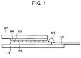
- As shown in Fig. 1, a
probe board 114 for supporting a plurality ofprobe electrodes 113 and alead wire board 119 are provided on aprobe base board 115, and theprobe electrodes 113 and thelead wire board 119 are electrically connected with respect to therespective probe electrodes 113 by connectingwires 118 such as wire bonding. On the other hand, arecording medium 116 supported by arecording medium plate 117 is arranged to face the plane of theprobe plate 114 on which the probe electrodes are provided. A pulsive voltage for writing a record bit on therecording medium 116 by a recording/reproducing voltage application circuit (not shown) is applied between therecording medium 116 and each of theprobe electrodes 113, and a read voltage for reading the written information is applied to record and reproduce the information. - However, in the conventional recording and reproducing apparatus described above, the probe plate and the recording medium are in a very close position in the recording and reproducing modes. As a result, unless the electric lead wires from the probe plate are optimally designed, the connecting wires which are connecting parts with the lead wire plate interfere with the recording medium plate or the recording medium, so that there will arise a problem that the connecting wires are shorted each other or the connecting wires are broken. This problem is serious particularly when the probe electrodes and the recording medium are relatively moved in a plane by a large distance.
- JP -A- 4 289 580 and US -A- 5 216 631 disclose an information recording and reproducing apparatus for performing recording and reproducing of information by using a probe electrode comprising a probe electrode supported by a probe plate and arranged to face a recording medium supported by a recording medium plate; moving means for relatively moving that recording medium and said probe electrode; voltage application means for applying a voltage between said recording medium and said probe electrode; and an electric wire take-out portion provided in a plane of said probe plate opposite to said probe electrode.
- US -A- 5 094 975 discloses a method of making a microscopic multi probe consisting of a multiplicity of densely populated microscopic probes having sharp apices. Such a probe plate is made from single crystalline silicon. Further an aluminium lead is disclosed connecting the probes with a tunnel current processing apparatus, which processes the signals taken out of the probes.
- WO -A- 9015986 discloses microfabricated microscope structures used in tunnelling microscopes and atomic force microscopes, which incorporate a surface to be scanned and a cantilever arm having a scanning tip at the end thereof.
- It is an object of the present invention to provide an information recording and reproducing apparatus which optimize the wiring of the lead wires from the probe plate.
- The above object is achieved by the features of
claims -
- Fig. 1 shows a sectional view of a neighborhood of a probe plate and a recording medium for illustrating a positional relationship between the probe plate and the recording medium in a conventional information recording and reproducing apparatus,
- Fig. 2 shows a block diagram of one embodiment of the information recording and reproducing apparatus of the present invention,
- Fig. 3 shows a sectional view of a neighborhood of a cantilever of the probe plate shown in Fig. 1,
- Fig. 4 shows a sectional view of a neighborhood of the probe plate and the recording medium for illustrating a positional relation between the probe plate and the recording medium shown in Fig. 1,
- Fig. 5 shows a perspective view of a probe plate and an electric circuit board shown in Fig. 4,
- Fig. 6 shows a sectional view of a neighborhood of a cantilever of a probe plate in other embodiment of the information recording and reproducing apparatus of the present invention, and
- Fig. 7 shows a sectional view of the recording medium shown in Fig. 4.
-
- An embodiment of the present invention is now explained with reference to the drawings.
- Fig. 2 shows a block diagram of one embodiment of the information recording and reproducing apparatus of the present invention. As shown in Fig. 2,
conductive probe electrodes 1 are fixed to free ends ofcantilevers 2 made of elastic material. The fixed ends of thecantilevers 2 are fixed to aprobe plate 3 made of a silicon single crystal substrate. Anxy drive element 6 including a piezo-electric element has one end thereof fixed to theprobe plate 3 and the other end thereof fixed to an inside of amain body 7, so that theprobe electrodes 1 can be driven in xy directions by thexy drive element 6. Accordingly, theprobe electrodes 1 can be moved to any position in the xy direction. - On the other hand, a
recording medium 8 includes a record layer having a Squarilium-Bis-6-n-Octylazulene (SOAZ) dye organic thin film deposited on a gold electrode, and the gold electrode of therecording medium 8 is formed on amedium plate 80. Az drive element 9 including a piezo-electric element has one end thereof fixed to themedium substrate 80 and the other end fixed to the inside of themain body 7, so that themedium plate 80 is driven in the z direction by thez drive element 9 and therecording medium 8 is moved in the z direction. As seen from the above description, the drive means for relatively moving theprobe electrodes 1 and therecording medium 8 is constituted by thexy drive element 6 and thez drive element 9. - A
probe position controller 10 controls the z position of the probe electrodes 1 (a spacing between theprobe electrode 1 and the recording medium 8) and the xy position of theprobe electrodes 1 by instruction of signal processing, or signal fromtiming controller 13 or switchingcircuit 11, and it is connected to thexy drive element 6 and thez drive element 9. Theswitching circuit 11 switches signals to theprobe electrodes 1 by a signal from thetiming controller 13, and switches the signal from theprobe electrodes 1 and transmits it to awaveform shaping circuit 14. A recording/reproducingvoltage application circuit 12 which serves as voltage application means applies a pulsive voltage to write a record bit, to therecording medium 8 by a signal from thetiming controller 13, and applies a read voltage to read the written information. Thetiming controller 13 is connected to theprobe position controller 10, theswitching circuit 11 and the recording/reproducingvoltage application circuit 12 to control the time division processing of the recorded and reproduced data and the allocation of the record signals to the probe electrodes. Thewaveform shaping circuit 14 which serves as current detection means detects a current flowing between therecording medium 8 and theprobe electrodes 1 to reproduce the information recorded by the signal from theprobe electrodes 1. - A structure of the
probe plate 3 is explained in detail with reference to Fig. 3. Fig. 3 shows a sectional view of a neighborhood of a cantilever of the probe plate shown in Fig. 2. As shown in Fig. 3, thecantilever 2 to which theprobe electrode 1 is fixed is made by depositing aresilient oxide film 20 and anelectrical signal wire 40. Theprobe electrode 1 is electrically connected to theelectrical signal wire 40. The fixed end of thecantilever 2 is fixed to one plane of theprobe plate 3 made of a silicon single crystal plate, and an electricalwire lead portion 4 is formed on the other plane of theprobe plate 3. The electricwire lead portion 4 includes aconductive member 41, aconductive film 42 having a metal vapor-deposited thereon, and a leadingwire 43 by wire bonding which serves as an electrical wire for taking out an electrical signal out of theprobe plate 3. An electrical signal from theprobe electrode 1 flows to theelectrical signal wire 40, theconductive member 41, theconductive film 42 and thelead wire 43 sequentially, whereby the electrical signal is taken out to the plane of theprobe plate 3 opposite to theprobe electrode 1. - The
electric wire lead 4 of the present embodiment is formed in the following manner. Ions are implanted to that portion of the silicon single crystal substrate (probe plate 3) having both sides thereof polished which is to be formed into theconductive member 41. Then, an area from a rear side (an upper plane in Fig. 3) of the silicon single crystal to the ion implanted portion which is to be formed into theconductive member 41 is electrolytically etched by potassium hydroxide (KOH) solution. Thus, theconductive member 41 is formed at the bottom of the hole formed by the etching. Then, chromium (Cr) is evaporated on to the hole through a mask, and gold (Au) is applied to form theconductive film 42. A bonding pad for the wire bonding is provided on theconductive film 42 as connecting means. - The
probe electrodes 1 and thecantilevers 2 are formed in the following manner. A thermal oxidization film is formed on a silicon single crystal substrate to a thickness of 0.3 µm, and asmany oxide films 20 as the number ofcantilevers 2 to be formed, which are of lever shape having a length of 100 µm and a width of 20 µm, are patterned. A pattern of theelectrical signal wire 40 is then formed on theoxide film 20 and a predetermined portion of the silicon single crystal substrate is etched by potassium hydroxide (KOH) solution from the upper surface to form thecantilevers 2. Then, carbon (C) is deposited to a height of 5 µm at the ends of thecantilevers 2 by an electron beam deposition method to form theprobe electrodes 1. - A positional relationship between the
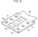
probe plate 3 and the recording medium 8 (see Fig. 2) is now explained with reference to Figs. 4 and 5. Fig. 4 shows a sectional view of a neighborhood of the probe plate and the recording medium for illustrating the positional relationship between the probe plate and the recording medium shown in Fig. 2, and Fig. 5 shows a perspective view of the probe substrate and the electric circuit board shown in Fig. 4. As shown in Figs. 4 and 5, an electric circuit board 5 (which includes the circuits 10-14 of Fig. 2) for effecting the control is attached to the plane of theprobe plate 3 opposite to theprobe electrode 1, and thelead wires 43 are connected to the signal wires through a bonding pad (not shown) formed in theelectric wiring area 51 of theelectric circuit board 5 from theelectric wire lead 4 formed on theprobe plate 3.Electric parts 52 for processing the signals from theprobe electrodes 1 are mounted on theelectric circuit board 5 and they are connected to the control unit through anexternal connection unit 53 having a flexible printed circuit board. Therecording medium 8 is arranged to face theprobe electrodes 1. - In the present construction, only the
probe electrodes 1 project to the plane of theprobe plate 3 facing therecording medium 8. Thus, when theprobe plate 3 and therecording medium 8 are relatively moved in a plane, thelead wires 43 do not interfere with therecording medium 8. As a result, the degree of freedom in arranging theprobe substrate 3 and therecording medium 8 is increased. Further, since the electric signal wires from theprobe electrodes 1 are connected to the electric circuit in short paths without routing theprobe plate 3, the circuit is resistable to disturbance. - Fig. 6 shows a sectional view of a neighborhood of the cantilevers of the probe plate in another embodiment of the information recording and reproducing apparatus of the present invention. In the present embodiment, the
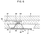
conductive probe electrodes 1 are fixed to free ends of thecantilevers 2 having a resilient andconductive film 21 andelectrical signal wires 40 and they are electrically connected to theconductive film 21 and theelectrical signal wires 40. The fixed ends of thecantilevers 2 are fixed to theprobe plate 3 made of a silicon single crystal substrate. Theelectrical wire lead 4 includeselectrical signal wires 40,conductive film 21,conductive wires 44 having metal evaporated thereon, and ametal bump 45 formed to take out the electrical signals out of theprobe plate 3. The electrical signal from theprobe electrode 1 sequentially flowes to theconductive film 21, theelectrical signal wires 40, theconductive wires 44 and thebump 45, so that the electrical signal is taken out of the plane of theprobe plate 3 opposite to theprobe electrodes 1. Theprobe plate 3 and theelectric circuit board 5 are electrically connected by usingconductive particles 47 contained in an anisotropicallyconductive sheet 46 between thebump 45 facing theprobe plate 3 and theelectrode pad 55 facing theelectric circuit board 5. The recording medium (not shown) is arranged to face theprobe electrodes 1. - The
probe plate 3 of the present embodiment is formed in the following manner. Ions are implanted to a silicon single crystal substrate having both sides thereof polished to form a conductive member, and a plurality of lever shapedconductive films 21 having a length of 150 µm and a width of 30 µm are patterned (only one lever is shown in Fig. 6). Then, a pattern of theelectrical signal wires 40 is formed and electrolytic etching is conducted by potassium hydroxide (KOH) solution to the ion implanted area from a rear side (upper surface in Fig. 6) of the silicon single crystal substrate. Thus, thecantilevers 2 and the levers with short electrical wire leads are formed. Chromium (Cr) is evaporated to the short levers through a mask, and gold (Au) is applied to form theconductive wires 44. Thebumps 45 for the anisotropicallyconductive sheet 46 are provided on theconductive wires 44. Then, carbon (C) is deposited to a height of 5 µm at the ends of thecantilevers 2 by an electron beam deposition method to form theprobe electrodes 1. In this manner, theprobe electrodes 1 are formed at the ends of thecantilevers 2 on theprobe plate 3. - The
probe plate 3 and theelectric circuit board 5 are connected in the following manner. The anisotropicallyconductive sheet 46 having a number ofconductive particles 47 uniformly dispersed in the bond is positioned between theprobe plate 3 and theelectric circuit board 5, and it is heated and pressurized so that theconductive particles 47 are physically contacted only vertically (between thebump 45 and the electrode pad 55) to make it anisotropically conductive. - In the present embodiment, like in the embodiment shown in Fig. 3, only the
probe electrodes 1 project to the plane of theprobe plate 3 opposite to the recording medium (not shown). Accordingly, when theprobe plate 3 and the recording medium are relatively moved in the plane, theconductive wires 44 do not interfere with the recording medium. Further, since theelectrical signal wires 40 from theprobe electrodes 1 can be connected to theelectric circuit board 5 in a short path without routing to theprobe plate 3, the circuit is resistable to disturbance. - In the embodiments described above, the electrical wires are taken out from the neighborhood of the
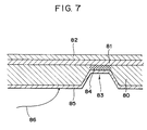
probe electrodes 1 to the opposite side of theprobe substrate 3 although the present provided on theprobe plate 3 and the electric wires may be taken out of the end of theprobe plate 3. The position to taken out to the opposite side of theprobe plate 3 is not limited to that described in the embodiments. Further, while theprobe plate 3 is described in connection with the take-out of the electric wires, it may be applied to the medium plate 80 (Fig. 4). - This is explained in detail with reference to Fig. 7.
Numeral 80 denotes a recording medium plate made of a silicon single crystal substrate, numeral 81 denotes a recording medium underlying electrode having gold (Au) epitaxially grown, numeral 82 denotes a record layer having a Squarilium-Bis-6-n-Octylazulene (SOAZ) dye organic thin film deposited on the recording medium underlying substrate by an LB method, numeral 83 denotes an electric wire take-out portion formed on the plane of the recording medium plate opposite to the record layer, numeral 84 denotes a conductive member, numeral 85 denotes a conductive film having gold evaporated, and numeral 86 denotes an electrical wire for taking the electrical signal out of therecording medium plate 80. Thus, the information signal from therecord layer 82 flows to the recordingmedium underlying electrode 81, theconductive member 84, theconductive film 85 and thelead wire 86 sequentially, so that the information signal may be taken out from the plane of therecording medium substrate 80 opposite to the record layer. - The
electric wire lead 83 in the present embodiment is formed in the same manner as that of theelectric wire lead 4 of Fig. 3. It is also effective where the underlying electrode of therecording medium 8 is divided into a plurality of portions. The electrical connection between theprobe plate 3 and theelectrical circuit board 5 may be made by soldering but preferably it is made by solderless mounting method such as conductive bond connection, conductive plated resin ball connection or direct connection by gold bump and insulative resin. - The present invention offers the following advantages.
- Since the electric wire lead for taking out the electric wire is provided on at least one of the plane of the probe plate opposite to the probe electrodes and the plane of the recording medium plate opposite to the recording medium, there is no projecting member other than the probe electrodes between the probe plate and the recording medium. Thus, when the probe electrodes and the recording medium are relatively moved in the plane, the electric wires do not interfere with the recording medium or the probe electrodes. As a result, the recording and reproducing apparatus having a high degree of freedom in arranging the probe plate and the recording medium substrate is attained.
- Further, since it is not necessary to route the electric wires on the plate, the length of the electric wires can be shortened and the signal from the probe electrodes is resistive to the external disturbance and the design of the probe plate having a plurality of probe electrodes is facilitated.
Claims (4)
- An information recording and reproducing apparatus for performing at least one of recording of information into and reproducing of information from a recording medium, comprising:a recording medium (8);a probe electrode (1) supported by one plane of a probe plate (3) and arranged to face said recording medium (8);moving means (6, 9) for relatively moving said recording medium (8) and said probe electrode (1); andvoltage application means (12) for applying a voltage between said recording medium (8) and said probe electrode (1);
characterized in thata conductive film (42) for taking out an electrical wire is formed on the other plane of said probe plate (3), said probe plate (3) is made of a semiconductor material, said probe plate (3) has an ion-implanted, conductive region (41) formed as passing through the probe plate (3), and said probe electrode (1) and said conductive film (42) are electrically connected to each other through said conductive region (41). - An information recording and reproducing apparatus for performing at least one of recording of information into and reproducing of information from a recording medium, comprising:a recording medium (8);a probe electrode (1) supported by one plane of a probe plate (3) and arranged to face said recording medium (8);moving means (6,9) for relatively moving said recording medium (8) and said probe electrode (1);voltage application means (12) for applying a voltage between said recording medium (8) and said probe electrode (1); andan electrical circuit board (5) for processing signals taken out of said probe electrode (1),
characterized in thata conductive film (45) electrically connected to said probe electrode (1) is formed on the other plane of said probe plate (3), said electrical circuit board (5) is laminated on said other plane of said probe plate (3) with interposing an anisotropically conductive sheet (46), said electrical circuit board (5) has an electrode pad (55) at a position opposite to the conductive film of said probe plate (3), and said conductive film (45) and said electrode pad (55) are electrically connected to each other through said anisotropically conductive sheet (46). - An apparatus according to claim 1 or 2, wherein said probe plate (3) is a single crystal semiconductor substrate.
- An apparatus according to claim 3, wherein said probe plate (3) is a single crystal silicon substrate.
Applications Claiming Priority (3)
| Application Number | Priority Date | Filing Date | Title |
|---|---|---|---|
| JP34075492 | 1992-12-21 | ||
| JP4340754A JP3025120B2 (en) | 1992-12-21 | 1992-12-21 | Recording and playback device |
| JP340754/92 | 1992-12-21 |
Publications (3)
| Publication Number | Publication Date |
|---|---|
| EP0603770A2 EP0603770A2 (en) | 1994-06-29 |
| EP0603770A3 EP0603770A3 (en) | 1995-12-13 |
| EP0603770B1 true EP0603770B1 (en) | 2000-03-08 |
Family
ID=18339990
Family Applications (1)
| Application Number | Title | Priority Date | Filing Date |
|---|---|---|---|
| EP93120440A Expired - Lifetime EP0603770B1 (en) | 1992-12-21 | 1993-12-17 | Information recording and reproducing apparatus for recording and reproducing information by using a probe electrode |
Country Status (6)
| Country | Link |
|---|---|
| US (1) | US5426631A (en) |
| EP (1) | EP0603770B1 (en) |
| JP (1) | JP3025120B2 (en) |
| AT (1) | ATE190424T1 (en) |
| CA (1) | CA2111770C (en) |
| DE (1) | DE69328012T2 (en) |
Families Citing this family (37)
| Publication number | Priority date | Publication date | Assignee | Title |
|---|---|---|---|---|
| US6337479B1 (en) | 1994-07-28 | 2002-01-08 | Victor B. Kley | Object inspection and/or modification system and method |
| US6339217B1 (en) | 1995-07-28 | 2002-01-15 | General Nanotechnology Llc | Scanning probe microscope assembly and method for making spectrophotometric, near-field, and scanning probe measurements |
| US6353219B1 (en) | 1994-07-28 | 2002-03-05 | Victor B. Kley | Object inspection and/or modification system and method |
| US5751683A (en) | 1995-07-24 | 1998-05-12 | General Nanotechnology, L.L.C. | Nanometer scale data storage device and associated positioning system |
| JPH09293283A (en) * | 1996-04-25 | 1997-11-11 | Hewlett Packard Co <Hp> | Probe device, its manufacture and media movement type memory device |
| JPH10321631A (en) * | 1997-05-19 | 1998-12-04 | Oki Electric Ind Co Ltd | Semiconductor device and its manufacture |
| US6459088B1 (en) * | 1998-01-16 | 2002-10-01 | Canon Kabushiki Kaisha | Drive stage and scanning probe microscope and information recording/reproducing apparatus using the same |
| US6787768B1 (en) | 2001-03-08 | 2004-09-07 | General Nanotechnology Llc | Method and apparatus for tool and tip design for nanomachining and measurement |
| US7196328B1 (en) | 2001-03-08 | 2007-03-27 | General Nanotechnology Llc | Nanomachining method and apparatus |
| US6802646B1 (en) * | 2001-04-30 | 2004-10-12 | General Nanotechnology Llc | Low-friction moving interfaces in micromachines and nanomachines |
| US6752008B1 (en) | 2001-03-08 | 2004-06-22 | General Nanotechnology Llc | Method and apparatus for scanning in scanning probe microscopy and presenting results |
| US6923044B1 (en) | 2001-03-08 | 2005-08-02 | General Nanotechnology Llc | Active cantilever for nanomachining and metrology |
| AU6061100A (en) * | 1999-07-01 | 2001-01-22 | General Nanotechnology, Llc | Object inspection and/or modification system and method |
| US6931710B2 (en) | 2001-01-30 | 2005-08-23 | General Nanotechnology Llc | Manufacturing of micro-objects such as miniature diamond tool tips |
| US7253407B1 (en) | 2001-03-08 | 2007-08-07 | General Nanotechnology Llc | Active cantilever for nanomachining and metrology |
| US20020154871A1 (en) * | 2001-04-19 | 2002-10-24 | Autonetworks Technologies, Ltd. | Optical connector, shield casing, optical connector device |
| JP4695325B2 (en) * | 2001-09-17 | 2011-06-08 | キヤノン電子株式会社 | Magnetic detection element, method of manufacturing the same, and portable device using the element |
| US7053369B1 (en) * | 2001-10-19 | 2006-05-30 | Rave Llc | Scan data collection for better overall data accuracy |
| US6813937B2 (en) * | 2001-11-28 | 2004-11-09 | General Nanotechnology Llc | Method and apparatus for micromachines, microstructures, nanomachines and nanostructures |
| EP1539637A4 (en) | 2002-09-09 | 2010-07-28 | Gen Nanotechnology Llc | Fluid delivery for scanning probe microscopy |
| US20050128927A1 (en) * | 2003-12-15 | 2005-06-16 | Hewlett-Packard Development Co., L.P. | Electrostatic actuator for contact probe storage device |
| US7436753B2 (en) | 2003-12-17 | 2008-10-14 | Mejia Robert G | Contact probe storage FET sensor |
| US7423954B2 (en) * | 2003-12-17 | 2008-09-09 | Hewlett-Packard Development Company, L.P. | Contact probe storage sensor pod |
| US7212487B2 (en) * | 2004-01-07 | 2007-05-01 | Hewlett-Packard Development Company, L.P. | Data readout arrangement |
| US7787350B2 (en) * | 2005-01-13 | 2010-08-31 | International Business Machines Corporation | Data storage device |
| US7212488B2 (en) | 2005-03-21 | 2007-05-01 | Hewlett-Packard Development Company, L.P. | Method and device enabling capacitive probe-based data storage readout |
| JP2007141414A (en) * | 2005-11-22 | 2007-06-07 | Lg Electronics Inc | Nano information saving/reproduction device using cantilever structure, and its manufacturing method |
| US8302456B2 (en) | 2006-02-23 | 2012-11-06 | Asylum Research Corporation | Active damping of high speed scanning probe microscope components |
| US7514942B2 (en) * | 2006-09-27 | 2009-04-07 | Intel Corporation | Probe based patterning of microelectronic and micromechanical devices |
| US7948337B2 (en) * | 2007-05-31 | 2011-05-24 | Seagate Technology Llc | Simultaneous rotational control using offset linear actuators |
| JP2009123421A (en) * | 2007-11-13 | 2009-06-04 | Canon Inc | Method of manufacturing air tight container |
| JP2011210430A (en) * | 2010-03-29 | 2011-10-20 | Canon Inc | Method for manufacturing hermetic container |
| JP2011210431A (en) * | 2010-03-29 | 2011-10-20 | Canon Inc | Method for manufacturing hermetic container |
| JP5590935B2 (en) * | 2010-03-29 | 2014-09-17 | キヤノン株式会社 | Airtight container manufacturing method |
| JP2012059401A (en) | 2010-09-06 | 2012-03-22 | Canon Inc | Method for manufacturing airtight container |
| JP5627370B2 (en) | 2010-09-27 | 2014-11-19 | キヤノン株式会社 | Depressurized airtight container and image display device manufacturing method |
| US9383388B2 (en) | 2014-04-21 | 2016-07-05 | Oxford Instruments Asylum Research, Inc | Automated atomic force microscope and the operation thereof |
Family Cites Families (15)
| Publication number | Priority date | Publication date | Assignee | Title |
|---|---|---|---|---|
| US4575822A (en) * | 1983-02-15 | 1986-03-11 | The Board Of Trustees Of The Leland Stanford Junior University | Method and means for data storage using tunnel current data readout |
| FR2559297B1 (en) * | 1984-02-03 | 1990-01-12 | Commissariat Energie Atomique | NEW FLIGHT SKATE FOR MAGNETIC RECORDING HEADS |
| DE3679319D1 (en) * | 1986-05-27 | 1991-06-20 | Ibm | STORAGE UNIT WITH DIRECT ACCESS. |
| US4916688A (en) * | 1988-03-31 | 1990-04-10 | International Business Machines Corporation | Data storage method using state transformable materials |
| JPH01290598A (en) * | 1988-05-17 | 1989-11-22 | Res Dev Corp Of Japan | Production of fine multiprobe |
| JP2896794B2 (en) * | 1988-09-30 | 1999-05-31 | キヤノン株式会社 | Scanning tunnel current detector, scanning tunnel microscope, and recording / reproducing device |
| US5015850A (en) * | 1989-06-20 | 1991-05-14 | The Board Of Trustees Of The Leland Stanford Junior University | Microfabricated microscope assembly |
| DE69126830T2 (en) * | 1990-08-14 | 1997-11-20 | Canon Kk | Bending beam measuring sensor and information processing device equipped with the measuring sensor |
| JP3030574B2 (en) * | 1990-08-16 | 2000-04-10 | キヤノン株式会社 | Micro-displacement information detecting probe element, scanning tunnel microscope, atomic force microscope, and information processing apparatus using the same |
| JP2741629B2 (en) * | 1990-10-09 | 1998-04-22 | キヤノン株式会社 | Cantilever probe, scanning tunneling microscope and information processing apparatus using the same |
| JP2802828B2 (en) * | 1990-10-19 | 1998-09-24 | キヤノン株式会社 | Information record carrier and information processing apparatus using the same |
| US5216631A (en) * | 1990-11-02 | 1993-06-01 | Sliwa Jr John W | Microvibratory memory device |
| JPH0575047A (en) * | 1991-03-08 | 1993-03-26 | Hitachi Ltd | Storage device |
| JP2930447B2 (en) * | 1991-05-15 | 1999-08-03 | キヤノン株式会社 | Information processing device |
| US5329122A (en) * | 1991-08-29 | 1994-07-12 | Canon Kabushiki Kaisha | Information processing apparatus and scanning tunnel microscope |
-
1992
- 1992-12-21 JP JP4340754A patent/JP3025120B2/en not_active Expired - Fee Related
-
1993
- 1993-12-16 US US08/167,140 patent/US5426631A/en not_active Expired - Lifetime
- 1993-12-17 DE DE69328012T patent/DE69328012T2/en not_active Expired - Fee Related
- 1993-12-17 EP EP93120440A patent/EP0603770B1/en not_active Expired - Lifetime
- 1993-12-17 AT AT93120440T patent/ATE190424T1/en not_active IP Right Cessation
- 1993-12-17 CA CA002111770A patent/CA2111770C/en not_active Expired - Fee Related
Also Published As
| Publication number | Publication date |
|---|---|
| US5426631A (en) | 1995-06-20 |
| DE69328012T2 (en) | 2000-08-03 |
| EP0603770A2 (en) | 1994-06-29 |
| ATE190424T1 (en) | 2000-03-15 |
| CA2111770A1 (en) | 1994-06-22 |
| EP0603770A3 (en) | 1995-12-13 |
| DE69328012D1 (en) | 2000-04-13 |
| CA2111770C (en) | 1998-10-13 |
| JP3025120B2 (en) | 2000-03-27 |
| JPH06195773A (en) | 1994-07-15 |
Similar Documents
| Publication | Publication Date | Title |
|---|---|---|
| EP0603770B1 (en) | Information recording and reproducing apparatus for recording and reproducing information by using a probe electrode | |
| US5015850A (en) | Microfabricated microscope assembly | |
| US5412641A (en) | Information recording/reproducing apparatus for recording/reproducing information with probes | |
| US7099115B2 (en) | Head gimbal assembly with precise positioning actuator for head element, disk drive apparatus with the head gimbal assembly, and manufacturing method of the head gimbal assembly | |
| JP2614412B2 (en) | Magnetic transducer / suspension assembly and manufacturing method, and magnetic disk drive system | |
| US4998016A (en) | Probe unit, driving method thereof, and scanning device for detecting tunnel current having said probe unit | |
| US7059868B1 (en) | Connection of trace circuitry in a computer disk drive system | |
| US6671131B2 (en) | Precise positioning actuator for head element, head gimbal assembly with the actuator and manufacturing method of head gimbal assembly | |
| USRE36538E (en) | Combination transducer/slider/suspension and method for making | |
| JP3148946B2 (en) | Probe driving mechanism, tunnel current detecting device using the mechanism, information processing device, piezoelectric actuator | |
| US8111487B2 (en) | Electromagnetic heads, flexures, gimbals and actuators formed on and from a wafer substrate | |
| US20010001588A1 (en) | Integrated lead head supension assembly having an etched laminated load beam and flexure with deposited conductors | |
| JP2001503552A (en) | Bimorph piezoelectric microactuator head and flexure assembly | |
| KR100304023B1 (en) | Milliactuator with integrated sensor and drivers and method manufacturing the same | |
| JPH04157640A (en) | Information recording carrier and information processing using the same | |
| US20020154450A1 (en) | Precise positioning actuator for head element, head gimbal assembly with the actuator and manufacturing method of actuator | |
| US6512313B2 (en) | Electromagnetic X-Y stage driver for nano data storage system and method for fabricating coils of the same | |
| KR100369279B1 (en) | A transducer suspension with high conductivity leads | |
| US20030142447A1 (en) | Disk apparatus, wiring body for disk apparatus and method of manufacturing the wiring body for disk apparatus | |
| JP3126527B2 (en) | Information processing device | |
| US6751061B2 (en) | Magnetic head, and device and method for manufacturing the same | |
| JP3053971B2 (en) | Three-dimensional displacement element for generating tunnel current, multi-tip unit using the three-dimensional displacement element for generating tunnel current, and information processing apparatus | |
| JP2934057B2 (en) | Probe unit and information recording and / or reproducing apparatus using the same | |
| JP2936291B2 (en) | Recording medium, information processing apparatus using the same, and recording medium cassette | |
| JPH04157642A (en) | Information recording carrier and information processing using the same |
Legal Events
| Date | Code | Title | Description |
|---|---|---|---|
| PUAI | Public reference made under article 153(3) epc to a published international application that has entered the european phase |
Free format text: ORIGINAL CODE: 0009012 |
|
| AK | Designated contracting states |
Kind code of ref document: A2 Designated state(s): AT BE CH DE DK ES FR GB GR IT LI LU NL PT SE |
|
| PUAL | Search report despatched |
Free format text: ORIGINAL CODE: 0009013 |
|
| AK | Designated contracting states |
Kind code of ref document: A3 Designated state(s): AT BE CH DE DK ES FR GB GR IT LI LU NL PT SE |
|
| 17P | Request for examination filed |
Effective date: 19960613 |
|
| 17Q | First examination report despatched |
Effective date: 19980526 |
|
| GRAG | Despatch of communication of intention to grant |
Free format text: ORIGINAL CODE: EPIDOS AGRA |
|
| GRAG | Despatch of communication of intention to grant |
Free format text: ORIGINAL CODE: EPIDOS AGRA |
|
| GRAH | Despatch of communication of intention to grant a patent |
Free format text: ORIGINAL CODE: EPIDOS IGRA |
|
| GRAH | Despatch of communication of intention to grant a patent |
Free format text: ORIGINAL CODE: EPIDOS IGRA |
|
| GRAA | (expected) grant |
Free format text: ORIGINAL CODE: 0009210 |
|
| AK | Designated contracting states |
Kind code of ref document: B1 Designated state(s): AT BE CH DE DK ES FR GB GR IT LI LU NL PT SE |
|
| PG25 | Lapsed in a contracting state [announced via postgrant information from national office to epo] |
Ref country code: SE Free format text: THE PATENT HAS BEEN ANNULLED BY A DECISION OF A NATIONAL AUTHORITY Effective date: 20000308 Ref country code: NL Free format text: LAPSE BECAUSE OF FAILURE TO SUBMIT A TRANSLATION OF THE DESCRIPTION OR TO PAY THE FEE WITHIN THE PRESCRIBED TIME-LIMIT Effective date: 20000308 Ref country code: LI Free format text: LAPSE BECAUSE OF NON-PAYMENT OF DUE FEES Effective date: 20000308 Ref country code: IT Free format text: LAPSE BECAUSE OF FAILURE TO SUBMIT A TRANSLATION OF THE DESCRIPTION OR TO PAY THE FEE WITHIN THE PRE;WARNING: LAPSES OF ITALIAN PATENTS WITH EFFECTIVE DATE BEFORE 2007 MAY HAVE OCCURRED AT ANY TIME BEFORE 2007. THE CORRECT EFFECTIVE DATE MAY BE DIFFERENT FROM THE ONE RECORDED.SCRIBED TIME-LIMIT Effective date: 20000308 Ref country code: GR Free format text: LAPSE BECAUSE OF NON-PAYMENT OF DUE FEES Effective date: 20000308 Ref country code: ES Free format text: THE PATENT HAS BEEN ANNULLED BY A DECISION OF A NATIONAL AUTHORITY Effective date: 20000308 Ref country code: CH Free format text: LAPSE BECAUSE OF NON-PAYMENT OF DUE FEES Effective date: 20000308 Ref country code: BE Free format text: LAPSE BECAUSE OF FAILURE TO SUBMIT A TRANSLATION OF THE DESCRIPTION OR TO PAY THE FEE WITHIN THE PRESCRIBED TIME-LIMIT Effective date: 20000308 Ref country code: AT Free format text: LAPSE BECAUSE OF FAILURE TO SUBMIT A TRANSLATION OF THE DESCRIPTION OR TO PAY THE FEE WITHIN THE PRESCRIBED TIME-LIMIT Effective date: 20000308 |
|
| REF | Corresponds to: |
Ref document number: 190424 Country of ref document: AT Date of ref document: 20000315 Kind code of ref document: T |
|
| REG | Reference to a national code |
Ref country code: CH Ref legal event code: EP |
|
| REF | Corresponds to: |
Ref document number: 69328012 Country of ref document: DE Date of ref document: 20000413 |
|
| ET | Fr: translation filed | ||
| PG25 | Lapsed in a contracting state [announced via postgrant information from national office to epo] |
Ref country code: PT Free format text: LAPSE BECAUSE OF FAILURE TO SUBMIT A TRANSLATION OF THE DESCRIPTION OR TO PAY THE FEE WITHIN THE PRESCRIBED TIME-LIMIT Effective date: 20000608 Ref country code: DK Free format text: LAPSE BECAUSE OF FAILURE TO SUBMIT A TRANSLATION OF THE DESCRIPTION OR TO PAY THE FEE WITHIN THE PRESCRIBED TIME-LIMIT Effective date: 20000608 |
|
| NLV1 | Nl: lapsed or annulled due to failure to fulfill the requirements of art. 29p and 29m of the patents act | ||
| REG | Reference to a national code |
Ref country code: CH Ref legal event code: PL |
|
| PG25 | Lapsed in a contracting state [announced via postgrant information from national office to epo] |
Ref country code: LU Free format text: LAPSE BECAUSE OF NON-PAYMENT OF DUE FEES Effective date: 20001217 |
|
| PLBE | No opposition filed within time limit |
Free format text: ORIGINAL CODE: 0009261 |
|
| STAA | Information on the status of an ep patent application or granted ep patent |
Free format text: STATUS: NO OPPOSITION FILED WITHIN TIME LIMIT |
|
| 26N | No opposition filed | ||
| REG | Reference to a national code |
Ref country code: GB Ref legal event code: IF02 |
|
| PGFP | Annual fee paid to national office [announced via postgrant information from national office to epo] |
Ref country code: DE Payment date: 20041209 Year of fee payment: 12 |
|
| PGFP | Annual fee paid to national office [announced via postgrant information from national office to epo] |
Ref country code: GB Payment date: 20041215 Year of fee payment: 12 |
|
| PGFP | Annual fee paid to national office [announced via postgrant information from national office to epo] |
Ref country code: FR Payment date: 20051208 Year of fee payment: 13 |
|
| PG25 | Lapsed in a contracting state [announced via postgrant information from national office to epo] |
Ref country code: GB Free format text: LAPSE BECAUSE OF NON-PAYMENT OF DUE FEES Effective date: 20051217 |
|
| PG25 | Lapsed in a contracting state [announced via postgrant information from national office to epo] |
Ref country code: DE Free format text: LAPSE BECAUSE OF NON-PAYMENT OF DUE FEES Effective date: 20060701 |
|
| GBPC | Gb: european patent ceased through non-payment of renewal fee |
Effective date: 20051217 |
|
| REG | Reference to a national code |
Ref country code: FR Ref legal event code: ST Effective date: 20070831 |
|
| PG25 | Lapsed in a contracting state [announced via postgrant information from national office to epo] |
Ref country code: FR Free format text: LAPSE BECAUSE OF NON-PAYMENT OF DUE FEES Effective date: 20070102 |