EP0603106A2 - Method to reduce stress from trench structure on SOI wafer - Google Patents
Method to reduce stress from trench structure on SOI wafer Download PDFInfo
- Publication number
- EP0603106A2 EP0603106A2 EP93480199A EP93480199A EP0603106A2 EP 0603106 A2 EP0603106 A2 EP 0603106A2 EP 93480199 A EP93480199 A EP 93480199A EP 93480199 A EP93480199 A EP 93480199A EP 0603106 A2 EP0603106 A2 EP 0603106A2
- Authority
- EP
- European Patent Office
- Prior art keywords
- layer
- trench
- silicon
- silicon layer
- insulator
- Prior art date
- Legal status (The legal status is an assumption and is not a legal conclusion. Google has not performed a legal analysis and makes no representation as to the accuracy of the status listed.)
- Withdrawn
Links
Images


Classifications
-
- H—ELECTRICITY
- H01—ELECTRIC ELEMENTS
- H01L—SEMICONDUCTOR DEVICES NOT COVERED BY CLASS H10
- H01L21/00—Processes or apparatus adapted for the manufacture or treatment of semiconductor or solid state devices or of parts thereof
- H01L21/70—Manufacture or treatment of devices consisting of a plurality of solid state components formed in or on a common substrate or of parts thereof; Manufacture of integrated circuit devices or of parts thereof
- H01L21/71—Manufacture of specific parts of devices defined in group H01L21/70
- H01L21/76—Making of isolation regions between components
- H01L21/762—Dielectric regions, e.g. EPIC dielectric isolation, LOCOS; Trench refilling techniques, SOI technology, use of channel stoppers
- H01L21/7624—Dielectric regions, e.g. EPIC dielectric isolation, LOCOS; Trench refilling techniques, SOI technology, use of channel stoppers using semiconductor on insulator [SOI] technology
- H01L21/76264—SOI together with lateral isolation, e.g. using local oxidation of silicon, or dielectric or polycristalline material refilled trench or air gap isolation regions, e.g. completely isolated semiconductor islands
-
- H—ELECTRICITY
- H01—ELECTRIC ELEMENTS
- H01L—SEMICONDUCTOR DEVICES NOT COVERED BY CLASS H10
- H01L21/00—Processes or apparatus adapted for the manufacture or treatment of semiconductor or solid state devices or of parts thereof
- H01L21/02—Manufacture or treatment of semiconductor devices or of parts thereof
- H01L21/04—Manufacture or treatment of semiconductor devices or of parts thereof the devices having at least one potential-jump barrier or surface barrier, e.g. PN junction, depletion layer or carrier concentration layer
- H01L21/18—Manufacture or treatment of semiconductor devices or of parts thereof the devices having at least one potential-jump barrier or surface barrier, e.g. PN junction, depletion layer or carrier concentration layer the devices having semiconductor bodies comprising elements of Group IV of the Periodic System or AIIIBV compounds with or without impurities, e.g. doping materials
- H01L21/30—Treatment of semiconductor bodies using processes or apparatus not provided for in groups H01L21/20 - H01L21/26
- H01L21/302—Treatment of semiconductor bodies using processes or apparatus not provided for in groups H01L21/20 - H01L21/26 to change their surface-physical characteristics or shape, e.g. etching, polishing, cutting
- H01L21/306—Chemical or electrical treatment, e.g. electrolytic etching
- H01L21/3065—Plasma etching; Reactive-ion etching
-
- H—ELECTRICITY
- H01—ELECTRIC ELEMENTS
- H01L—SEMICONDUCTOR DEVICES NOT COVERED BY CLASS H10
- H01L21/00—Processes or apparatus adapted for the manufacture or treatment of semiconductor or solid state devices or of parts thereof
- H01L21/70—Manufacture or treatment of devices consisting of a plurality of solid state components formed in or on a common substrate or of parts thereof; Manufacture of integrated circuit devices or of parts thereof
- H01L21/71—Manufacture of specific parts of devices defined in group H01L21/70
- H01L21/76—Making of isolation regions between components
- H01L21/763—Polycrystalline semiconductor regions
-
- H—ELECTRICITY
- H01—ELECTRIC ELEMENTS
- H01L—SEMICONDUCTOR DEVICES NOT COVERED BY CLASS H10
- H01L21/00—Processes or apparatus adapted for the manufacture or treatment of semiconductor or solid state devices or of parts thereof
- H01L21/70—Manufacture or treatment of devices consisting of a plurality of solid state components formed in or on a common substrate or of parts thereof; Manufacture of integrated circuit devices or of parts thereof
- H01L21/71—Manufacture of specific parts of devices defined in group H01L21/70
- H01L21/76—Making of isolation regions between components
- H01L21/762—Dielectric regions, e.g. EPIC dielectric isolation, LOCOS; Trench refilling techniques, SOI technology, use of channel stoppers
- H01L21/7624—Dielectric regions, e.g. EPIC dielectric isolation, LOCOS; Trench refilling techniques, SOI technology, use of channel stoppers using semiconductor on insulator [SOI] technology
- H01L21/76264—SOI together with lateral isolation, e.g. using local oxidation of silicon, or dielectric or polycristalline material refilled trench or air gap isolation regions, e.g. completely isolated semiconductor islands
- H01L21/76286—Lateral isolation by refilling of trenches with polycristalline material
Definitions
- the present invention generally relates to an improved isolation trench geometry for trenches formed in silicon-on-oxide wafers, and more particularly to a geometry that reduces structural stress in the trench wall, and includes a process for forming such isolation trenches.
- the thickness of the top silicon layer of a silicon-on-insulator wafer will vary from 0.05 ⁇ m to 15 ⁇ m.
- SOI device applications can be divided into three categories: (a) high density, low power digital CMOS applications where a thin silicon layer (about 0.05 to 0.2 ⁇ m) is desirable to form fully depleted MOS devices; (b) medium density, high speed and low voltage digital BiCMOS applications where a silicon thickness of 1.5 to 3.0 ⁇ m is needed in order to achieve optimum bipolar performance, i.e., high cut-off frequency; and (c) low density, high speed and high voltage analog BiCMOS devices where a large silicon thickness ranging from 8 to 15 ⁇ m is necessary in order to withstand high voltage operation.
- the prior art isolation recess or trench can develop regions of large stress. Ion implantation in these stress regions can result in a nucleate glide dislocation that can cause shorts or leakage in transistors.
- An object of this invention is the provision of a silicon-on-insulator isolation trench free of geometrics that result in high stress in the silicon trench wall.
- Another object of this invention is the provision of a method of forming a silicon-on-insulator isolation trench so that the trench sidewall is free of high stress producing sidewall geometries.
- this invention contemplates the provision of an isolation trench in a silicon-on-insulator wafer in which the sidewalls of the trench curve outwardly at the bottom of the trench where the top silicon layer meets the underlying oxide insulating layer.
- This sidewall geometry eliminates the sharp corner at the bottom of the trench.
- the top edge of the trench wall is also curved.
- a trench etch is used that has a highly selective etch rate of silicon as compared to oxide.
- an SF6/Cl2 plasma etches silicon at a rate that is 12 times faster than it etches silicon oxide.
- the vertical etch rate is significantly reduced.
- Over etching the trench into the oxide layer results primarily in a lateral undercutting at the bottom of the silicon trench walls. Any one of several methods can be used to determine when the top surface of the sub-oxide layer is reached; optical emission, a laser interferometer, or the etch can be timed.
- the degree of outward curvature can be controlled by controlling the duration of the over etch after the sub-oxide layer is reached.
- the top edge of the trench is rounded by ion sputtering during a final stage of the trench formation.
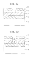
- Figures 1A through 1G illustrate a trench structure in accordance with the teachings of this invention at successive stages in its fabrication;
- Figure 1E shows the completed trench structure with the sidewall of the trench curved outwardly at the bottom of the trench.
- FIG. 1A it shows a fragmentary, sectional view of a conventional silicon-on-insulator wafer for a medium density, high speed, low voltage digital BiCMOS applications.
- the wafer is comprised of a semiconductor substrate 10, a silicon-oxide (SiO2) layer 12, and a single crystal silicon layer 14 whose thickness is on the order of between 1.5 ⁇ m and 3.0 ⁇ m.
- a suitable masking oxide layer 16 is deposited on the top surface of the silicon layer 14 and a photoresist layer 30 is formed in the oxide mask layer 16.
- the photoresist 30 is developed in the desired trench pattern and an opening for the trench is formed in the oxide mask 16 by means of well-known semiconductor process steps.
- an isolation trench 20 is formed in the top single crystal silicon layer 14 so that its sidewalls 22, at the bottom of the trench curve outwardly from the center of the trench.
- the radius of outward curvature R should be in a range between that of the sidewall oxide thickness (between 50 nm and 100 nm) and 25% of the thickness of the silicon layer 14.
- an etching process is used that etches the silicon layer 14 selectively at a much higher rate than it etches the silicon-oxide layer 12.
- a conventional SF6 /Cl2 plasma etching process is suitable as it has a selectivity ratio of 12 to 1; that is, a SF6 /Cl2 plasma etches the silicon layer 14 at twelve times the rate it etches the silicon-oxide layer 12.
- Other suitable known etching processes are Cl2 /O2 plasma which has a similar selectivity.
- the top surface of the sublayer oxide 12 can be detected by a suitable method such as optical emission, laser interferometer or timing the etch. Typically, by monitoring Cl emission line (wavelength 308 nm) a reproducible end point characteristic can be obtained. Normally several large end point test sites are located on the wafer. The degree of convexness of the silicon bottom can be controlled by controlling the percentage of overetch.
- the top corners 24 of the trench sidewalls are also slightly rounded to further reduce points of stress.
- the photoresist layer 30 is pulled back slightly from the trench opening by means, for example, of an O 2 plasma etch that exposes a small region 23 of the surface of the oxide layer 16, as shown in Figure 1C.
- the exposed surface of the oxide layer 16 is trimmed away by means of a CF4 plasma etch step to expose the top corners of the trench in silicon layer 14.
- the structure at this stage is shown in Figure 1D.
- a Cl 2O2 plasma etch for a brief interval is used to cut away and thereby round the top corners 24 of the trench sidewall as shown in Figure 1E.
- an oxide layer 31 is grown on the trench sidewalls using a suitable prior art process such as conventional thermal oxidation at 950°C or high pressure oxidation at 700°C to grow oxide about 60 nm thick as shown in igure 1F.
- the trench is then filled with polysilicon 32 using a conventional chemical vapor deposition process.
- the structure at this stage is shown in Figure 1G.
- a stress relief annealing step is preferably carried out at about 1050°G to 1100°C for about 20 minutes in a forming gas (e.g. 10% H2, 90°N2).
Abstract
In an isolation trench in a silicon-on-insulator wafer, the sidewalls of the trench curve outwardly at the bottom of the trench where the top silicon layer meets the underlying oxide insulating layer. A typical SOI structure is comprised of a semiconductor substrate (10), a silicon-oxide (SiO₂) layer 12, and a single crystal silicon layer (14). A suitable masking oxide layer (16) is deposited on the top surface of the silicon layer (14) and a photoresist (30) is formed thereon. The photoresist (30) is developed in the desired trench pattern and an opening for the trench is formed in the oxide mask (16) by means of well-known semiconductor process steps. An isolation trench (20) is formed in the top single crystal silicon layer (14) so that its sidewalls (22), at the bottom of the trench curve outwardly from the center of the trench. Preferably, the top corners (24) of the trench sidewalls are also slightly rounded to further reduce points of stress. After the trench is formed, the photoresist is removed and an oxide layer (31) is grown on the trench sidewalls using a conventional process. The trench is then filled with polysilicon (32) using a conventional chemical vapor deposition process. Finally, the structure is planarized. Optionally a stress relief annealing step is carried out at about 1050°C to 1100°C for about 20 minutes in a forming gas. This sidewall geometry eliminates the sharp corner at the bottom of the trench that are detrimental to device reliability.
Description
- The present invention generally relates to an improved isolation trench geometry for trenches formed in silicon-on-oxide wafers, and more particularly to a geometry that reduces structural stress in the trench wall, and includes a process for forming such isolation trenches.
- Building semiconductor devices on silicon-on-insulator (SOI) wafers is recent technology that has been introduced to improve circuit speed and device reliability. Depending on the circuit application, the thickness of the top silicon layer of a silicon-on-insulator wafer will vary from 0.05 µm to 15 µm. Normally, SOI device applications can be divided into three categories: (a) high density, low power digital CMOS applications where a thin silicon layer (about 0.05 to 0.2 µm) is desirable to form fully depleted MOS devices; (b) medium density, high speed and low voltage digital BiCMOS applications where a silicon thickness of 1.5 to 3.0 µm is needed in order to achieve optimum bipolar performance, i.e., high cut-off frequency; and (c) low density, high speed and high voltage analog BiCMOS devices where a large silicon thickness ranging from 8 to 15 µm is necessary in order to withstand high voltage operation.
- Since each of these three SOI devices requires a different range of silicon layer thickness and different integrated device density, quite different isolation schemes are needed. For case (a) with the thin SOI, the isolation is usually formed by using a conventional recess oxidation (ROX) process. For Case (b) with the medium thickness SOI, trench isolation with an oxide sidewall and polysilicon fill is used. Lastly in case (c) with the thick SOI where there is a power limitation which allows only low density integration, simple junction isolation is adequate.
- In cases (a) and (b), the prior art isolation recess or trench can develop regions of large stress. Ion implantation in these stress regions can result in a nucleate glide dislocation that can cause shorts or leakage in transistors.
- An object of this invention is the provision of a silicon-on-insulator isolation trench free of geometrics that result in high stress in the silicon trench wall.
- Another object of this invention is the provision of a method of forming a silicon-on-insulator isolation trench so that the trench sidewall is free of high stress producing sidewall geometries.
- Briefly, this invention contemplates the provision of an isolation trench in a silicon-on-insulator wafer in which the sidewalls of the trench curve outwardly at the bottom of the trench where the top silicon layer meets the underlying oxide insulating layer. This sidewall geometry eliminates the sharp corner at the bottom of the trench. Preferably, the top edge of the trench wall is also curved.
- To form the trench with an outwardly curving wall surface at the bottom of the trench, a trench etch is used that has a highly selective etch rate of silicon as compared to oxide. For example, an SF₆/Cl₂ plasma etches silicon at a rate that is 12 times faster than it etches silicon oxide. When the oxide layer of the silicon-on-insulator wafer is reached and exposed to such an etch, the vertical etch rate is significantly reduced. Over etching the trench into the oxide layer results primarily in a lateral undercutting at the bottom of the silicon trench walls. Any one of several methods can be used to determine when the top surface of the sub-oxide layer is reached; optical emission, a laser interferometer, or the etch can be timed. The degree of outward curvature can be controlled by controlling the duration of the over etch after the sub-oxide layer is reached. In a preferred embodiment, the top edge of the trench is rounded by ion sputtering during a final stage of the trench formation.
- The foregoing and other objects, aspects and advantages will be better understood from the following detailed description of a preferred embodiment of the invention with reference to the drawings, in which:
- Figures 1A through 1G illustrate a trench structure in accordance with the teachings of this invention at successive stages in its fabrication; Figure 1E shows the completed trench structure with the sidewall of the trench curved outwardly at the bottom of the trench.
- Referring now to Figure 1A, it shows a fragmentary, sectional view of a conventional silicon-on-insulator wafer for a medium density, high speed, low voltage digital BiCMOS applications. The wafer is comprised of a
semiconductor substrate 10, a silicon-oxide (SiO₂)layer 12, and a singlecrystal silicon layer 14 whose thickness is on the order of between 1.5 µm and 3.0 µm. A suitablemasking oxide layer 16 is deposited on the top surface of thesilicon layer 14 and aphotoresist layer 30 is formed in theoxide mask layer 16. Thephotoresist 30 is developed in the desired trench pattern and an opening for the trench is formed in theoxide mask 16 by means of well-known semiconductor process steps. - Referring now to Figure 1B, an
isolation trench 20 is formed in the top singlecrystal silicon layer 14 so that itssidewalls 22, at the bottom of the trench curve outwardly from the center of the trench. The radius of outward curvature R should be in a range between that of the sidewall oxide thickness (between 50 nm and 100 nm) and 25% of the thickness of thesilicon layer 14. - To form the
trench 20 withsidewalls 22 that curve outwardly from the bottom, an etching process is used that etches thesilicon layer 14 selectively at a much higher rate than it etches the silicon-oxide layer 12. For example, a conventional SF₆ /Cl₂ plasma etching process is suitable as it has a selectivity ratio of 12 to 1; that is, a SF₆ /Cl₂ plasma etches thesilicon layer 14 at twelve times the rate it etches the silicon-oxide layer 12. Other suitable known etching processes are Cl₂ /O₂ plasma which has a similar selectivity. When the etching process has proceeded to the point where the surface of theoxide layer 12 is exposed, the rate of vertical etching is greatly reduced. Continued etching beyond this point results in a lateral undercutting of thesilicon layer 14 at the bottom of the trench as shown in Figure 1B. The duration during which the etch process continues after the oxide layer is exposed, determines the radius of curvature R of the outwardly sloping sidewalls; the radius increases as the duration increases. - The top surface of the
sublayer oxide 12 can be detected by a suitable method such as optical emission, laser interferometer or timing the etch. Typically, by monitoring Cl emission line (wavelength 308 nm) a reproducible end point characteristic can be obtained. Normally several large end point test sites are located on the wafer. The degree of convexness of the silicon bottom can be controlled by controlling the percentage of overetch. - Preferably, the
top corners 24 of the trench sidewalls are also slightly rounded to further reduce points of stress. To this end, thephotoresist layer 30 is pulled back slightly from the trench opening by means, for example, of an O 2 plasma etch that exposes asmall region 23 of the surface of theoxide layer 16, as shown in Figure 1C. Next, the exposed surface of theoxide layer 16 is trimmed away by means of a CF₄ plasma etch step to expose the top corners of the trench insilicon layer 14. The structure at this stage is shown in Figure 1D. A Cl ₂O₂ plasma etch for a brief interval is used to cut away and thereby round thetop corners 24 of the trench sidewall as shown in Figure 1E. - After the trench is formed, the photoresist is removed, an
oxide layer 31 is grown on the trench sidewalls using a suitable prior art process such as conventional thermal oxidation at 950°C or high pressure oxidation at 700°C to grow oxide about 60 nm thick as shown in igure 1F. The trench is then filled withpolysilicon 32 using a conventional chemical vapor deposition process. After planarization, the structure at this stage is shown in Figure 1G. After the structure is completed to this stage, a stress relief annealing step is preferably carried out at about 1050°G to 1100°C for about 20 minutes in a forming gas (e.g. 10% H₂, 90°N₂).
Claims (9)
- In a silicon-on-insulator wafer comprised of a silicon layer on an insulating layer, an isolation trench formed by an opening in said silicon layer that extends from a top surface of said silicon layer to a top surface of said insulating layer, said opening formed by vertical sidewalls that each has a curved surface that curves away from a vertical center line of said opening where said sidewalls meet said top surface of said insulating layer.
- In a silicon-on-insulator wafer comprised of a silicon layer on an insulating layer, an isolation trench as in claim 1, wherein said curve has a radius of curvature in a range extending at the low end between 500Å and 1000Å to 25% of the thickness of said silicon layer.
- In a silicon-on-insulator wafer comprised of a silicon layer on an insulating layer, an isolation trench as in claim 1, wherein each of said vertical sidewalls is curved at said top surface of said silicon layer.
- In a silicon-on-insulator wafer comprised of a silicon layer on an insulating layer, an isolation trench as in claim 2, wherein each of said vertical sidewalls is curved at said top surface of said silicon layer.
- A method of forming an isolation trench in a silicon-on-insulator wafer including a silicon layer overlying an insulator layer, comprising the steps of:
etching through said silicon layer to said insulator layer with an etchant that selectively etches said silicon layer at a high rate compared with the rate at which it etches said insulator layer;
continuing the etching process of said previous step for a predetermined interval so that walls formed in said layer are undercut where they meet said insulator layer. - A method of forming an isolation trench in a silicon-on-insulator wafer including a silicon layer overlying an insulator layer, comprising the steps of:
etching a trench opening into said silicon layer through a masking layer that overlies said silicon layer, said trench opening forming a top edge at the upper surface of said silicon layer;
removing a small portion of said masking layer to expose a region of said silicon layer extending away from the top edges of said trench opening formed in the previous step;
etching said region of said silicon layer to form a curve at said top edges of said trench opening. - A method of forming an isolation trench in a silicon-on-insulator wafer including a silicon layer overlying an insulator layer, comprising the steps of:
etching through a masking layer that overlies said silicon layer to said insulator layer with an etchant that selectively etches said silicon layer at a high rate compared with the rate at which it etches said insulator layer;
continuing the etching process of said previous step for a predetermined interval so that walls formed in said layer are undercut where they meet said insulator layer with said trench opening forming a top edge at the upper surface of said silicon layer;
removing a small portion of said masking layer to expose a region of said silicon layer extending away from the top edges of said trench opening formed in the previous step;
etching said region of said silicon layer to form a curve at said top edges of said trench opening. - A method of forming an isolation trench in a silicon-on-insulator wafer including a silicon layer overlying an insulator layer as in claim 6, including the further steps of annealing said silicon-on-insulator wafer in a forming atmosphere.
- A method of forming an isolation trench in a silicon-on-insulator wafer including a silicon layer overlying an insulator layer as in claim 7, including the further steps of annealing said silicon-on-insulator wafer in a forming atmosphere.
Applications Claiming Priority (2)
| Application Number | Priority Date | Filing Date | Title |
|---|---|---|---|
| US99101092A | 1992-12-16 | 1992-12-16 | |
| US991010 | 1992-12-16 |
Publications (1)
| Publication Number | Publication Date |
|---|---|
| EP0603106A2 true EP0603106A2 (en) | 1994-06-22 |
Family
ID=25536752
Family Applications (1)
| Application Number | Title | Priority Date | Filing Date |
|---|---|---|---|
| EP93480199A Withdrawn EP0603106A2 (en) | 1992-12-16 | 1993-11-19 | Method to reduce stress from trench structure on SOI wafer |
Country Status (3)
| Country | Link |
|---|---|
| US (1) | US5470781A (en) |
| EP (1) | EP0603106A2 (en) |
| JP (1) | JP2531492B2 (en) |
Cited By (4)
| Publication number | Priority date | Publication date | Assignee | Title |
|---|---|---|---|---|
| US6355538B1 (en) * | 2000-09-18 | 2002-03-12 | Vanguard International Semiconductor Corporation | Method of forming isolation material with edge extension structure |
| GB2369494A (en) * | 2000-08-17 | 2002-05-29 | Samsung Electronics Co Ltd | Methods of preventing bending of SOI layer during trench refill |
| US6902867B2 (en) | 2002-10-02 | 2005-06-07 | Lexmark International, Inc. | Ink jet printheads and methods therefor |
| WO2005098936A1 (en) * | 2004-04-07 | 2005-10-20 | X-Fab Semiconductor Foundries Ag | Creation of dielectrically insulating soi-technological trenches comprising rounded edges for allowing higher voltages |
Families Citing this family (21)
| Publication number | Priority date | Publication date | Assignee | Title |
|---|---|---|---|---|
| JP3396553B2 (en) * | 1994-02-04 | 2003-04-14 | 三菱電機株式会社 | Semiconductor device manufacturing method and semiconductor device |
| JP3504025B2 (en) * | 1995-06-06 | 2004-03-08 | 三菱電機株式会社 | Semiconductor device and manufacturing method thereof |
| TW309647B (en) * | 1995-12-30 | 1997-07-01 | Hyundai Electronics Ind | |
| FR2750535B1 (en) * | 1996-06-27 | 1998-08-07 | Commissariat Energie Atomique | MOS TRANSISTOR AND METHOD FOR LATERAL ISOLATION OF AN ACTIVE REGION OF A MOS TRANSISTOR |
| US5914280A (en) * | 1996-12-23 | 1999-06-22 | Harris Corporation | Deep trench etch on bonded silicon wafer |
| US6265282B1 (en) | 1998-08-17 | 2001-07-24 | Micron Technology, Inc. | Process for making an isolation structure |
| US6127215A (en) * | 1998-10-29 | 2000-10-03 | International Business Machines Corp. | Deep pivot mask for enhanced buried-channel PFET performance and reliability |
| US6372599B1 (en) | 1999-01-14 | 2002-04-16 | Mitsubishi Denki Kabushiki Kaisha | Semiconductor device and method of manufacturing the same |
| US6514805B2 (en) * | 2001-06-30 | 2003-02-04 | Intel Corporation | Trench sidewall profile for device isolation |
| US20030194871A1 (en) * | 2002-04-15 | 2003-10-16 | Macronix International Co., Ltd. | Method of stress and damage elimination during formation of isolation device |
| US6984015B2 (en) * | 2003-08-12 | 2006-01-10 | Lexmark International, Inc. | Ink jet printheads and method therefor |
| JP4613565B2 (en) * | 2004-09-29 | 2011-01-19 | 株式会社デンソー | Semiconductor device and manufacturing method thereof |
| EP1844495B1 (en) * | 2005-01-24 | 2011-07-27 | Panasonic Corporation | Manufacturing method for semiconductor chips |
| JP2006269551A (en) * | 2005-03-22 | 2006-10-05 | Renesas Technology Corp | Semiconductor device and its manufacturing method |
| EP1930708A1 (en) | 2005-09-06 | 2008-06-11 | Ntn Corporation | Sensor-equipped bearing for wheel |
| WO2007066593A1 (en) | 2005-12-08 | 2007-06-14 | Ntn Corporation | Sensor-equipped bearing for wheel |
| JP5089041B2 (en) | 2005-12-08 | 2012-12-05 | Ntn株式会社 | Wheel bearing with sensor |
| US7856893B2 (en) | 2006-03-08 | 2010-12-28 | Ntn Corporation | Bearing for wheel with sensor |
| WO2008026305A1 (en) | 2006-08-25 | 2008-03-06 | Ntn Corporation | Sensor-equipped bearing for wheel |
| CN104517887B (en) * | 2013-09-27 | 2018-07-20 | 中芯国际集成电路制造(上海)有限公司 | A method of making semiconductor devices |
| JP5849112B2 (en) * | 2014-02-03 | 2016-01-27 | 株式会社 日立パワーデバイス | Semiconductor device |
Family Cites Families (7)
| Publication number | Priority date | Publication date | Assignee | Title |
|---|---|---|---|---|
| JPS62183138A (en) * | 1986-02-06 | 1987-08-11 | Fujitsu Ltd | Element isolation of semiconductor device |
| JPS6390828A (en) * | 1986-10-04 | 1988-04-21 | Sony Corp | Dry etching |
| JPS63314844A (en) * | 1987-06-18 | 1988-12-22 | Toshiba Corp | Manufacture of semiconductor device |
| JPH03129854A (en) * | 1989-10-16 | 1991-06-03 | Toshiba Corp | Manufacture of semiconductor device |
| US5196373A (en) * | 1990-08-06 | 1993-03-23 | Harris Corporation | Method of making trench conductor and crossunder architecture |
| JP3208575B2 (en) * | 1991-08-16 | 2001-09-17 | ソニー株式会社 | Semiconductor device manufacturing method |
| US5416041A (en) * | 1993-09-27 | 1995-05-16 | Siemens Aktiengesellschaft | Method for producing an insulating trench in an SOI substrate |
-
1993
- 1993-11-19 EP EP93480199A patent/EP0603106A2/en not_active Withdrawn
- 1993-11-24 JP JP5293503A patent/JP2531492B2/en not_active Expired - Fee Related
- 1993-12-14 US US08/166,415 patent/US5470781A/en not_active Expired - Fee Related
Cited By (8)
| Publication number | Priority date | Publication date | Assignee | Title |
|---|---|---|---|---|
| GB2369494A (en) * | 2000-08-17 | 2002-05-29 | Samsung Electronics Co Ltd | Methods of preventing bending of SOI layer during trench refill |
| GB2369494B (en) * | 2000-08-17 | 2003-04-23 | Samsung Electronics Co Ltd | Method of preventing semiconductor layers from bending and semiconductor deviceformed thereby |
| US6881645B2 (en) | 2000-08-17 | 2005-04-19 | Samsung Electronics Co., Ltd. | Method of preventing semiconductor layers from bending and semiconductor device formed thereby |
| DE10134484B4 (en) * | 2000-08-17 | 2006-06-29 | Samsung Electronics Co., Ltd., Suwon | A method of preventing bending of semiconductor layers and semiconductor device manufactured by the method |
| US6355538B1 (en) * | 2000-09-18 | 2002-03-12 | Vanguard International Semiconductor Corporation | Method of forming isolation material with edge extension structure |
| US6902867B2 (en) | 2002-10-02 | 2005-06-07 | Lexmark International, Inc. | Ink jet printheads and methods therefor |
| WO2005098936A1 (en) * | 2004-04-07 | 2005-10-20 | X-Fab Semiconductor Foundries Ag | Creation of dielectrically insulating soi-technological trenches comprising rounded edges for allowing higher voltages |
| US7989308B2 (en) | 2004-04-07 | 2011-08-02 | X-Fab Semiconductor Foundries Ag | Creation of dielectrically insulating soi-technlogical trenches comprising rounded edges for allowing higher voltages |
Also Published As
| Publication number | Publication date |
|---|---|
| US5470781A (en) | 1995-11-28 |
| JPH06216230A (en) | 1994-08-05 |
| JP2531492B2 (en) | 1996-09-04 |
Similar Documents
| Publication | Publication Date | Title |
|---|---|---|
| US5470781A (en) | Method to reduce stress from trench structure on SOI wafer | |
| USRE35294E (en) | Polysilicon encapsulated localized oxidation of silicon | |
| US4604162A (en) | Formation and planarization of silicon-on-insulator structures | |
| US5807789A (en) | Method for forming a shallow trench with tapered profile and round corners for the application of shallow trench isolation (STI) | |
| US4845048A (en) | Method of fabricating semiconductor device | |
| US4954459A (en) | Method of planarization of topologies in integrated circuit structures | |
| EP0258311B1 (en) | Process for forming isolation trenches in a semiconductor substrate | |
| US5795811A (en) | Method for forming insulating films in semiconductor devices | |
| US6051511A (en) | Method and apparatus for reducing isolation stress in integrated circuits | |
| US5747377A (en) | Process for forming shallow trench isolation | |
| EP0316550A2 (en) | Trench isolation means and method | |
| US4929566A (en) | Method of making dielectrically isolated integrated circuits using oxygen implantation and expitaxial growth | |
| US20010012676A1 (en) | Isolation Region forming methods | |
| JPH0645431A (en) | Process for formation of planar quasi- micrometric groove in integrated circuit manufactured by ulsi technique | |
| JPH03171632A (en) | Transistor and its manufacture | |
| US5512509A (en) | Method for forming an isolation layer in a semiconductor device | |
| US4661832A (en) | Total dielectric isolation for integrated circuits | |
| US6001705A (en) | Process for realizing trench structures | |
| US5242853A (en) | Manufacturing process for a semiconductor device using bias ecrcvd and an etch stop layer | |
| US5371035A (en) | Method for forming electrical isolation in an integrated circuit device | |
| US5185286A (en) | Process for producing laminated semiconductor substrate | |
| US5371036A (en) | Locos technology with narrow silicon trench | |
| EP0068275B1 (en) | Method for producing semiconductor devices including the use of reactive ion etching | |
| US4810668A (en) | Semiconductor device element-isolation by oxidation of polysilicon in trench | |
| EP0589124B1 (en) | Method for eliminating the bird's beak from selective oxidations of semiconductor electronic devices |
Legal Events
| Date | Code | Title | Description |
|---|---|---|---|
| PUAI | Public reference made under article 153(3) epc to a published international application that has entered the european phase |
Free format text: ORIGINAL CODE: 0009012 |
|
| AK | Designated contracting states |
Kind code of ref document: A2 Designated state(s): DE FR GB |
|
| 17P | Request for examination filed |
Effective date: 19941021 |
|
| STAA | Information on the status of an ep patent application or granted ep patent |
Free format text: STATUS: THE APPLICATION HAS BEEN WITHDRAWN |
|
| 18W | Application withdrawn |
Withdrawal date: 19961015 |