EP0600267A1 - Bidirektionaler optischer Sende- und Empfangsmodul - Google Patents
Bidirektionaler optischer Sende- und Empfangsmodul Download PDFInfo
- Publication number
- EP0600267A1 EP0600267A1 EP93118078A EP93118078A EP0600267A1 EP 0600267 A1 EP0600267 A1 EP 0600267A1 EP 93118078 A EP93118078 A EP 93118078A EP 93118078 A EP93118078 A EP 93118078A EP 0600267 A1 EP0600267 A1 EP 0600267A1
- Authority
- EP
- European Patent Office
- Prior art keywords
- laser diode
- substrate
- photodiode
- waveguide
- radiation
- Prior art date
- Legal status (The legal status is an assumption and is not a legal conclusion. Google has not performed a legal analysis and makes no representation as to the accuracy of the status listed.)
- Granted
Links
- 230000003287 optical effect Effects 0.000 title claims abstract description 13
- 230000002457 bidirectional effect Effects 0.000 title claims abstract description 6
- 239000000758 substrate Substances 0.000 claims abstract description 43
- 230000005855 radiation Effects 0.000 claims abstract description 28
- 239000002184 metal Substances 0.000 claims description 7
- 239000013307 optical fiber Substances 0.000 abstract description 4
- 239000003365 glass fiber Substances 0.000 description 15
- 239000000463 material Substances 0.000 description 10
- 230000005540 biological transmission Effects 0.000 description 9
- 230000008878 coupling Effects 0.000 description 7
- 238000010168 coupling process Methods 0.000 description 7
- 238000005859 coupling reaction Methods 0.000 description 7
- 239000004065 semiconductor Substances 0.000 description 6
- VYPSYNLAJGMNEJ-UHFFFAOYSA-N Silicium dioxide Chemical compound O=[Si]=O VYPSYNLAJGMNEJ-UHFFFAOYSA-N 0.000 description 4
- 229910001218 Gallium arsenide Inorganic materials 0.000 description 2
- XUIMIQQOPSSXEZ-UHFFFAOYSA-N Silicon Chemical compound [Si] XUIMIQQOPSSXEZ-UHFFFAOYSA-N 0.000 description 2
- 230000003667 anti-reflective effect Effects 0.000 description 2
- 229910052681 coesite Inorganic materials 0.000 description 2
- 229910052906 cristobalite Inorganic materials 0.000 description 2
- 238000005516 engineering process Methods 0.000 description 2
- 230000005693 optoelectronics Effects 0.000 description 2
- 229910052710 silicon Inorganic materials 0.000 description 2
- 239000010703 silicon Substances 0.000 description 2
- 239000000377 silicon dioxide Substances 0.000 description 2
- 235000012239 silicon dioxide Nutrition 0.000 description 2
- 229910052682 stishovite Inorganic materials 0.000 description 2
- 230000007704 transition Effects 0.000 description 2
- 229910052905 tridymite Inorganic materials 0.000 description 2
- 239000013078 crystal Substances 0.000 description 1
- 230000001419 dependent effect Effects 0.000 description 1
- 239000003989 dielectric material Substances 0.000 description 1
- 238000001914 filtration Methods 0.000 description 1
- 230000017525 heat dissipation Effects 0.000 description 1
- 238000004519 manufacturing process Methods 0.000 description 1
- 238000000034 method Methods 0.000 description 1
- 239000000203 mixture Substances 0.000 description 1
Images
Classifications
-
- H—ELECTRICITY
- H04—ELECTRIC COMMUNICATION TECHNIQUE
- H04B—TRANSMISSION
- H04B10/00—Transmission systems employing electromagnetic waves other than radio-waves, e.g. infrared, visible or ultraviolet light, or employing corpuscular radiation, e.g. quantum communication
- H04B10/40—Transceivers
-
- G—PHYSICS
- G02—OPTICS
- G02B—OPTICAL ELEMENTS, SYSTEMS OR APPARATUS
- G02B6/00—Light guides; Structural details of arrangements comprising light guides and other optical elements, e.g. couplings
- G02B6/24—Coupling light guides
- G02B6/42—Coupling light guides with opto-electronic elements
- G02B6/4201—Packages, e.g. shape, construction, internal or external details
- G02B6/4246—Bidirectionally operating package structures
Definitions
- the present invention relates to an arrangement of a bidirectional optical transmission and reception module for connection to an optical fiber shared for transmission and reception.
- transmission modules and reception modules are expediently combined in such a way that the same glass fiber can be used for the transmission and for the reception signal.
- at least one laser diode as the transmitter and one photodiode as the receiver are to be arranged in such a way that an optical connection of the glass fiber connection to the laser diode and also to the photodiode can be realized by means of suitable reflecting or filtering intermediate elements. The technical effort involved in installing such an arrangement is considerable.
- the object of the present invention is to provide an arrangement for a bidirectional optical transmission and reception module which is simple to manufacture and which can optionally be combined with further transmission, reception or control components.
- the beam path between the connection for the glass fiber and the optoelectronic transmitting and receiving elements runs through a substrate, on the opposite upper side of which the radiation is deflected parallel to the substrate surface by means of mirrors and into strip-shaped waveguides is guided.
- One top of the substrate therefore carries the various functional elements, while the opposite side carries the strip-shaped waveguides, which produce the optical connections.
- a waveguide layer 2 composed of strip-shaped waveguides 41, 42 is applied to one upper side of this substrate 1.
- Advantageous materials for the substrate 1 are, for example, silicon, GaAs or InP.
- the waveguide layer 2 contains e.g. B. buried waveguide or ridge waveguide which are made of the corresponding substrate 1 semiconductor materials.
- the waveguides 41, 42 are made in a manner known per se from differently doped semiconductor material with different, for. B. ternary or quaternary, crystal composition (z. B. GaAlAs / GaAs, InGaAsP, InGaAlAs). Dielectrics (e.g.
- doped or undoped SiO2 can also be used.
- mirrors 5 which are arranged obliquely such that radiation from the substrate 1 is coupled into a waveguide and radiation from a waveguide is reflected into the substrate.
- the mirrors 5 are preferably inclined approximately 45 ° with respect to the direction of propagation of the radiation in the waveguides 41, 42, so that the entry and exit of light into or out of the one which is transparent to the radiation Substrate 1 takes place approximately perpendicular to the waveguide layer 2.
- the deflection of the radiation at the mirrors 5 takes place through total reflection.
- semiconductor material for the substrate 1 and for the waveguide layer 2 the reflection at the transition between the waveguide material and the substrate material is negligible. If SiO2 waveguides are used on a silicon substrate, an anti-reflective layer or sequence of anti-reflective layers is advantageously to be applied to the transition surface.
- At least one laser diode 6 as the transmitter and one photodiode 7 as the receiver are arranged on the opposite top of the substrate 1.
- an external waveguide e.g. B. a glass fiber 9.
- the beam path of the light coming from this glass fiber 9 into the arrangement is indicated by simple arrows.
- the radiation emitted by the laser diode 6 is indicated by double arrows.
- Fig. 2 shows a top view of this arrangement. It can be seen that the radiation from the glass fiber 9 is deflected into the waveguide 42 and carried on therein. Part of the radiation is coupled in the coupler 14 into a second waveguide 41 and at the end of this waveguide 41 is deflected towards the photodiode 7 by a mirror 5. This radiation is received in the photodiode 7.
- the radiation from the laser diode 6 passes into the waveguide 42 and at least part of this radiation from there into the glass fiber 9.
- filters that are opaque to the other wavelength can be installed in the beam path in front of the laser diode 6 and in front of the photodiode 7. In this way it is achieved that the wavelength to be received does not reach the laser diode 6 and that a wavelength emitted by the laser diode 6 is not detected by the photodiode 7.
- the additional arrangement of a filter layer 3 is expedient for such filters.
- the filter can also be used on the relevant surface of the substrate 1 can be integrated.
- the laser diode 6 is preferably a surface-emitting semiconductor laser which is mounted directly on the substrate or the filter layer 3 mentioned. 1 shows an edge-emitting laser diode 6 with an active layer 16 and a deflection mirror 15.
- the laser can also have an integrated microlens. Additional microlenses 12, which are arranged on the upper side of the substrate 1 in front of the laser diode 6 and in front of the photodiode 7, are also shown in FIG. 1. The heat dissipation of the laser takes place through the substrate 1 or via the filter layer 3. Optical crosstalk between the laser diode 6 and the photodiode 7 can additionally be reduced by enclosing the photodiode 7 with opaque material 19.
- the surface of the substrate 1 opposite the waveguide layer 2 can be provided with a metal layer 13 which has openings for unimpeded passage of the radiation.
- Scattered light is shielded with this metal layer 13 and a mounting surface for the functional elements (laser diode 6, photodiode 7) applied to this metal layer 13 is formed.
- an equipotential surface is formed by the metal, which can be electrically grounded against electrical crosstalk between the laser diode 6 and the photodiode 7.
- the arrangement according to the invention is characterized by a simple, compact design which can be easily assembled and adjusted from a few parts. It can be installed in a module housing and connected to the glass fiber 9 with a simple surface mounting, as is known from infrared diodes.
- a ball lens 10 (see FIG. 1) or lens plate (Fresnel, microlenses) to be added in this technique above the area provided for the connection of the glass fiber can also be mounted on the surface of the substrate 1.
- Fig. 1 is an anti-reflection layer for the light entry from this ball lens 10 into the substrate 1 11, which is formed in the filter layer 3, drawn.
- FIG. 3 shows an arrangement in which the glass fiber 9 is inserted directly into a recess in the substrate 1, the coupling surface being formed from the substrate material with an integrated lens 10.
- FIG. 3 shows a simplified arrangement in which there is no filter layer 3 and no metal layer 13.
- the laser diode 6 and the photodiode 7 are integrated in a layer sequence 17 of semiconductor material that has grown onto the upper side of the substrate 1.
- the intermediate region 18 of this layer sequence 17 between the laser diode 6 and the photodiode 7 is electrically and optically insulating. From the supervision of this arrangement in Fig.
- the substrate 1 may contain further components which are optically connected to one another via waveguides, with the coupling and uncoupling of light not generally having to take place via oblique mirrors 5, but e.g. B. can also be done in conventional technology with lenses, tapers or in butt coupling or leaky wave coupling.
- a particularly advantageous embodiment of the arrangement according to the invention provides a monitor diode 8 which serves to control the laser diode 6.
- This monitor diode 8 is as in Fig. 1 drawn so arranged that a portion of the light emitted by the laser diode 6 is supplied to it via a waveguide 41.
- Fig. 2 it can be seen that the said portion in this embodiment by means of the coupler 14 from the waveguide 42, which optically connects the laser diode 6 with the connection for the glass fiber, is coupled into the waveguide 41 and from there into the monitor diode 8 .
- the embodiment of FIG. 3 does not contain a monitor diode 8. The corresponding end of the waveguide 41 is blind.
- the glass fiber connection is connected to the laser diode 6 and to the photodiode 7, at least two waveguides are required in the case of strip-shaped waveguides with two ends.
- These waveguides can be coupled via a known waveguide coupler. It is also possible for the two waveguides to be brought together in a common strip (Y-shaped branching, which is to be understood as a coupler in the sense of claim 1), which is realized in particular in the exemplary embodiment of FIGS. 3 and 4 when the blind end of the waveguide 41 opens into the waveguide 42.
- Y-shaped branching which is to be understood as a coupler in the sense of claim 1
- a direct optical connection of the laser diode 6 with the connection via a common waveguide 42 is advantageous.
- a monitor diode 8 is provided, it is advantageous if a common waveguide 41, which is coupled to the other waveguide 42, is again provided for the other two components, namely the photodiode 7 and this monitor diode 8.
- the photodiode 7 and the connection for the external waveguide can be optically connected to one another via a common waveguide. The light coming from the laser diode 6 is deflected into another waveguide and into the waveguide optically connected to the glass fiber coupled. This arrangement can be advantageous if the incoming radiation does not have sufficient power for efficient coupling.
- the arrangement according to the invention is suitable for an operating mode in which the wavelengths of the radiation received and emitted are not clearly different from one another or in the case of transmission and reception not taking place simultaneously (so-called ping-pong operation).
- the arrangement according to the invention can also be extended to the use of a plurality of receiving and transmitting elements.
- Other functional elements such as. B. amplifiers or control circuits, can also be installed or integrated together with the laser diode 6 shown in the exemplary embodiments and the photodiode 7 in or on the substrate 1.
- a particular advantage of the arrangement is that one upper side of the substrate remains exclusively for the waveguide and all other elements can simply be grown or mounted on the opposite surface. Additional devices that filter, bundle or shield the radiation can be easily integrated into or onto the substrate.
Abstract
Description
- Die vorliegende Erfindung betrifft eine Anordnung eines bidirektionalen optischen Sende- und Empfangsmoduls für Anschluß an eine zum Senden und Empfangen gemeinsam benutzte Glasfaser.
- In der optoelektronischen Nachrichtentechnik werden Sendemodule und Empfangsmodule zweckmäßigerweise derart kombiniert, daß dieselbe Glasfaser für das Sende- und für das Empfangssignal verwendet werden kann. Bei den bidirektionalen Modulen sind mindestens eine Laserdiode als Sender und eine Fotodiode als Empfänger so anzuordnen, daß mittels geeigneter reflektierender oder filternder Zwischenelemente eine optische Verbindung des Glasfaseranschlusses sowohl mit der Laserdiode als auch mit der Fotodiode realisierbar ist. Der technische Aufwand bei der Montage einer derartigen Anordnung ist erheblich.
- Aufgabe der vorliegenden Erfindung ist es, eine Anordnung für einen bidirektionalen optischen Sende- und Empfangsmodul anzugeben, die einfach herstellbar ist und ggf. mit weiteren Sende-, Empfangs- oder Ansteuerkomponenten kombiniert werden kann.
- Diese Aufgabe wird mit der Anordnung mit den Merkmalen des Anspruches 1 gelöst. Weitere Ausgestaltungen ergeben sich aus den abhängigen Ansprüchen.
- Bei der erfindungsgemäßen Anordnung verläuft der Strahlengang zwischen dem Anschluß für die Glasfaser und den optoelektronischen Sende- und Empfangselementen durch ein Substrat, auf dessen gegenüberliegender Oberseite die Strahlung mittels Spiegeln parallel zur Substratoberfläche umgelenkt und in streifenförmigen Wellenleitern geführt wird. Die eine Oberseite des Substrates trägt daher die verschiedenen Funktionselemente, während die gegenüberliegende Seite die streifenförmigen Wellenleiter trägt, die die optischen Verbindungen herstellen.
- Es folgt eine Beschreibung der erfindungsgemäßen Anordnung anhand der Figuren 1 bis 4.
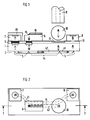
- Fig. 1 und 3
- zeigen zwei Ausführungsformen der erfindungsgemäßen Anordnung im Querschnitt.
- Fig. 2 und 4
- zeigen die den Fig. 1 bzw. 3 entsprechenden Anordnungen in Aufsicht.
- In Fig. 1 ist das Substrat 1 eingezeichnet, das eine Halbleiterscheibe oder allgemein eine Materialplatte mit ausreichender mechanischer Stabilität und optischer Transparenz sein kann. Auf der einen Oberseite dieses Substrates 1 ist eine Wellenleiterschicht 2 aus streifenförmigen Wellenleitern 41, 42 aufgebracht. Vorteilhafte Materialien für das Substrat 1 sind beispielsweise Silizium, GaAs oder InP. Die Wellenleiterschicht 2 enthält z. B. vergrabene Wellenleiter oder Stegwellenleiter die aus den dem jeweiligen Substrat 1 entsprechenden Halbleitermaterialien hergestellt sind. Die Wellenleiter 41, 42 sind in an sich bekannter Weise aus unterschiedlich dotiertem Halbleitermaterial mit unterschiedlicher, z. B. ternärer oder quaternärer, Kristallzusammensetzung (z. B. GaAlAs/GaAs, InGaAsP, InGaAlAs) hergestellt. Es können auch Dielektrika (z. B. dotiertes oder undotiertes SiO₂) verwendet werden. An Enden der Wellenleiter 41, 42 befinden sich Spiegel 5, die derart schräg angeordnet sind, daß Strahlung aus dem Substrat 1 in einen Wellenleiter eingekoppelt wird und Strahlung aus einem Wellenleiter in das Substrat reflektiert wird. Die Spiegel 5 sind vorzugsweise etwa 45° gegenüber der Ausbreitungsrichtung der Strahlung in den Wellenleitern 41, 42 geneigt, so daß der Lichteintritt und Lichtaustritt in bzw. aus dem für die Strahlung transparenten Substrat 1 etwa senkrecht zu der Wellenleiterschicht 2 erfolgt. Die Umlenkung der Strahlung an den Spiegeln 5 erfolgt dabei durch Totalreflexion. Bei Verwendung von Halbleitermaterial für das Substrat 1 und für die Wellenleiterschicht 2 ist die Reflexion am Übergang zwischen dem Wellenleitermaterial und dem Substratmaterial vernachlässigbar. Im Falle der Verwendung von SiO₂-Wellenleitern auf einem Siliziumsubstrat ist an der Übergangsfläche vorteilhaft eine Antireflexschicht oder Antireflexschichtfolge anzubringen.
- Auf der gegenüberliegenden Oberseite des Substrates 1 sind mindestens eine Laserdiode 6 als Sender und eine Fotodiode 7 als Empfänger angeordnet. Außerdem befindet sich auf dieser Seite ein Anschluß für einen externen Wellenleiter, z. B. eine Glasfaser 9. Der Strahlengang des aus dieser Glasfaser 9 in die Anordnung gelangenden Lichtes ist mit einfachen Pfeilen bezeichnet. Die von der Laserdiode 6 ausgesandte Strahlung ist jeweils mit Doppelpfeilen bezeichnet. Fig. 2 zeigt eine Aufsicht auf diese Anordnung. Es ist erkennbar, daß die Strahlung aus der Glasfaser 9 in den Wellenleiter 42 umgelenkt und darin weitergeführt wird. Ein Teil der Strahlung wird in dem Koppler 14 in einen zweiten Wellenleiter 41 übergekoppelt und am Ende dieses Wellenleiters 41 durch einen Spiegel 5 nach der Fotodiode 7 hin umgelenkt. In der Fotodiode 7 wird diese Strahlung empfangen. Die Strahlung von der Laserdiode 6 gelangt in den Wellenleiter 42 und zumindest ein Teil dieser Strahlung von da in die Glasfaser 9.
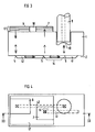
- Wenn die Sendewellenlange und die Empfangswellenlänge verschieden sind, können in den Strahlengang vor die Laserdiode 6 und vor die Fotodiode 7 jeweils für die andere Wellenlänge undurchlässige Filter eingebaut sein. Auf diese Weise erreicht man, daß die zu empfangende Wellenlänge nicht die Laserdiode 6 erreicht und daß eine von der Laserdiode 6 ausgesandte Wellenlänge nicht von der Fotodiode 7 detektiert wird. Für derartige Filter ist die zusätzliche Anordnung einer Filterschicht 3 zweckmäßig. Die Filter können aber auch an der betreffenden Oberfläche des Substrates 1 integriert sein. Die Laserdiode 6 ist vorzugsweise ein oberflächenemittierender Halbleiterlaser, der direkt auf das Substrat oder die erwähnte Filterschicht 3 montiert ist. In Fig. 1 ist eine kantenemittierende Laserdiode 6 mit einer aktiven Schicht 16 und einem Umlenkspiegel 15 gezeichnet. Zur Erhöhung des Einkoppelwirkungsgrades und der Justiertoleranz kann der Laser zusätzlich über eine integrierte Mikrolinse verfügen. Zusätzliche Mikrolinsen 12, die an der Oberseite des Substrates 1 vor der Laserdiode 6 und vor der Fotodiode 7 angeordnet sind, sind in Fig. 1 ebenfalls eingezeichnet. Die Wärmeabfuhr des Lasers erfolgt durch das Substrat 1 bzw. über die Filterschicht 3. Optisches Übersprechen zwischen der Laserdiode 6 und der Fotodiode 7 kann zusätzlich durch Umschließen der Fotodiode 7 mit lichtundurchlässigem Material 19 verringert werden. Die der Wellenleiterschicht 2 gegenüberliegende Oberfläche des Substrates 1 kann mit einer Metallschicht 13 versehen sein, die Öffnungen für ein ungehindertes Passieren der Strahlung aufweist. Mit dieser Metallschicht 13 wird Streulicht abgeschirmt und eine Montagefläche für die auf dieser Metallschicht 13 aufgebrachten Funktionselemente (Laserdiode 6, Fotodiode 7) gebildet. Außerdem wird durch das Metall eine Äquipotentialfläche gebildet, die gegen elektrisches Übersprechen zwischen der Laserdiode 6 und der Fotodiode 7 elektrisch geerdet werden kann.
- Die erfindungsgemäße Anordnung zeichnet sich durch eine einfache, kompakte Bauweise aus, die leicht aus wenigen Teilen zusammengesetzt und justiert werden kann. Sie kann mit einer einfachen Oberflächenmontage, wie sie von Infrarotdioden bekannt ist, in Modulgehäuse eingebaut und mit der Glasfaser 9 verbunden werden. Eine bei dieser Technik über dem für den Anschluß der Glasfaser vorgesehenen Bereich hinzuzufügende Kugellinse 10 (s. Fig. 1) oder Linsenplatte (Fresnel-, Mikrolinsen) kann ebenfalls auf der Oberfläche des Substrates 1 montiert werden. In Fig. 1 ist für den Lichteintritt aus dieser Kugellinse 10 in das Substrat 1 eine Antireflexionsschicht 11, die in der Filterschicht 3 ausgebildet ist, eingezeichnet. Fig. 3 zeigt eine Anordnung, bei der die Glasfaser 9 unmittelbar in einer Aussparung des Substrates 1 eingesetzt wird, wobei die Einkoppelfläche mit einer integrierten Linse 10 aus dem Substratmaterial gebildet wird. Bei der erfindungsgemäßen Anordnung ergibt sich keine Einschränkung dafür, wie der externe Wellenleiter angeschlossen wird. Deswegen sind in Fig. 1 keine weiteren Teile für die Montage der Glasfaser 9 und der Kugellinse 10 eingezeichnet. In Fig. 3 ist eine vereinfachte Anordnung dargestellt, bei der keine Filterschicht 3 und keine Metallschicht 13 vorhanden ist. Die Laserdiode 6 und die Fotodiode 7 sind in einer auf die Oberseite des Substrates 1 aufgewachsenen Schichtfolge 17 aus Halbleitermaterial integriert. Der Zwischenbereich 18 dieser Schichtfolge 17 zwischen der Laserdiode 6 und der Fotodiode 7 ist elektrisch und optisch isolierend. Aus der Aufsicht dieser Anordnung in Fig. 4 ist erkennbar, daß die Anordnung der streifenförmigen Wellenleiter 41, 42 bei diesem Ausführungsbeispiel anders ist. Der Strahlengang der ankommenden Strahlung (einfache Pfeile) und der ausgesandten Strahlung (Doppelpfeile) verläuft wieder über die Wellenleiter 41, 42 und wird mittels Spiegeln 5 umgelenkt. Durch die Figuren soll verdeutlicht werden, daß bei der erfindungsgemäßen Anordnung die Abmessungen und Abstände der Komponenten nicht festgelegt sind. Der Abstand zwischen Laserdiode 6 und Fotodiode 7 und die Form der Wellenleiter 41, 42 und die Lage des Anschlusses für den externen Wellenleiter sind variabel. Das Substrat 1 kann weitere Komponenten enthalten, die optisch über Wellenleiter miteinander verbunden werden, wobei das Ein- und Auskoppeln von Licht nicht grundsätzlich über schräge Spiegel 5 erfolgen muß, sondern z. B. auch in herkömmlicher Technik mit Linsen, Tapern oder in Stoßkopplung oder Leckwellenkopplung erfolgen kann.
- Eine besonders vorteilhafte Ausgestaltung der erfindungsgemäßen Anordnung sieht eine der Kontrolle der Laserdiode 6 dienende Monitordiode 8 vor. Diese Monitordiode 8 ist wie in Fig. 1 gezeichnet so angeordnet, daß ihr über einen Wellenleiter 41 ein Anteil des von der Laserdiode 6 ausgesandten Lichtes zugeführt wird. In Fig. 2 ist erkennbar, daß der besagte Anteil bei diesem Ausführungsbeispiel mittels des Kopplers 14 aus dem Wellenleiter 42, der die Laserdiode 6 optisch mit dem Anschluß für die Glasfaser verbindet, in den Wellenleiter 41 übergekoppelt wird und von da in die Monitordiode 8 gelangt. Das Ausführungsbeispiel der Fig. 3 enthält keine Monitordiode 8. Das entsprechende Ende des Wellenleiters 41 ist blind.
- Bei einer Verbindung des Glasfaseranschlusses mit der Laserdiode 6 und mit der Fotodiode 7 werden bei streifenförmigen Wellenleitern mit zwei Enden mindestens zwei Wellenleiter benötigt. Eine Kopplung dieser Wellenleiter kann über einen bekannten Wellenleiterkoppler erfolgen. Es ist auch möglich, daß beide Wellenleiter in einen gemeinsamen Streifen zusammengeführt werden (Y-förmige Verzweigung, die im Sinn des Anspruches 1 als Koppler aufzufassen ist), was insbesondere bei dem Ausführungsbeispiel der Fig. 3 und 4 realisiert ist, wenn das blinde Ende des Wellenleiters 41 in den Wellenleiter 42 einmündet. Eine einfache Anordnung ergibt sich, wenn möglichst wenige Wellenleiter miteinander verkoppelt werden müssen. Für eine effiziente Einkopplung der von der Laserdiode 6 ausgesandten Strahlung mit möglichst hoher Sendeleistung in die Glasfaser 9 ist eine direkte optische Verbindung der Laserdiode 6 mit dem Anschluß über einen gemeinsamen Wellenleiter 42 vorteilhaft. Falls eine Monitordiode 8 vorgesehen ist, ist es vorteilhaft, wenn für die übrigen beiden Komponenten, nämlich die Fotodiode 7 und diese Monitordiode 8, wieder ein gemeinsamer Wellenleiter 41, der mit dem anderen Wellenleiter 42 verkoppelt ist, vorgesehen ist. Alternativ dazu können die Fotodiode 7 und der Anschluß für den externen Wellenleiter über einen gemeinsamen Wellenleiter optisch miteinander verbunden sein. Das von der Laserdiode 6 kommende Licht wird in einen weiteren Wellenleiter umgelenkt und in den mit der Glasfaser optisch verbundenen Wellenleiter eingekoppelt. Diese Anordnung kann von Vorteil sein, wenn die ankommende Strahlung keine für ein effizientes Überkoppeln ausreichende Leistung besitzt.
- Die erfindungsgemäße Anordnung eignet sich für eine Betriebsweise, bei der die Wellenlängen der empfangenen und der ausgesandten Strahlung nicht deutlich voneinander verschieden sind oder bei der Senden und Empfangen nicht gleichzeitig erfolgen (sogenannter Ping-Pong-Betrieb).
- Die erfindungsgemäße Anordnung läßt sich auch auf den Einsatz mehrerer Empfangs- und Sendeelemente erweitern. Weitere Funktionselemente, wie z. B. Verstärker oder Ansteuerschaltungen, lassen sich zusätzlich montieren oder gemeinsam mit der in den Ausführungsbeispielen gezeichneten Laserdiode 6 und der Fotodiode 7 in oder auf das Substrat 1 integrieren. Ein besonderer Vorteil der Anordnung ist, daß die eine Oberseite des Substrates ausschließlich für die Wellenleiter vorgesehen bleibt und alle übrigen Elemente auf der gegenüberliegenden Oberfläche einfach aufgewachsen oder montiert werden können. Weitere dem Filtern, Bündeln oder Abschirmen der Strahlung dienende Einrichtungen lassen sich bequem in oder auf das Substrat integrieren.
Claims (7)
- Anordnung als bidirektionaler optischer Sende- und Empfangsmodul mit einem für optische Strahlung durchlässigen Substrat (1), mit mindestens zwei streifenförmigen Wellenleitern (41, 42), mit einem Anschluß für einen externen Wellenleiter (9) und mit mindestens einer Laserdiode (6) und einer Fotodiode (7),
bei der diese Wellenleiter (41, 42) auf einer Oberseite des Substrates (1) für Wellenführung parallel zu dieser Oberseite angeordnet sind,
bei der Enden dieser Wellenleiter (41, 42) mit Spiegeln (5) versehen sind, die so ausgerichtet sind, daß Strahlung zwischen Wellenleiter und Substrat reflektiert wird,
bei der dieser Anschluß, diese Laserdiode (6) und diese Fotodiode (7) auf der gegenüberliegenden Oberseite des Substrates (1) angeordnet und so ausgerichtet sind, daß von diesem externen Wellenleiter (9) oder von dieser Laserdiode (6) ausgehende Strahlung durch das Substrat (1) jeweils zu einem dieser Spiegel (5) am Ende eines Wellenleiters (42) gelangt und daß aus einem Wellenleiter (41) kommende Strahlung von einem dieser Spiegel (5) zu der Fotodiode (7) reflektiert wird, und bei der mindestens ein Koppler (14) zwischen zwei Wellenleitern (41, 42) derart vorgesehen ist, daß der Anschluß optisch mit der Laserdiode (6) und mit der Fotodiode (7) verbunden ist. - Anordnung nach Anspruch 1,
bei der eine weitere Fotodiode als Monitordiode (8) für die Laserdiode (6) vorgesehen ist,
bei der diese Monitordiode (8) auf derselben Oberfläche des Substrates (1) angeordnet ist wie die Laserdiode (6) und bei der ein Teil der von der Laserdiode (6) ausgesandten Strahlung von einem Spiegel (5) an einem Ende eines Wellenleiters (41) in diese Monitordiode (8) reflektiert wird. - Anordnung nach Anspruch 1 oder 2,
bei der die Laserdiode (6) und der Anschluß über denselben Wellenleiter (42) optisch verbunden sind. - Anordnung nach den Ansprüchen 1 bis 3,
bei der die Fotodiode (7) und die Monitordiode (8) über denselben Wellenleiter (41) optisch verbunden sind. - Anordnung nach einem der Ansprüche 1 bis 4,
bei der die Laserdiode (6) und die Fotodiode (7) auf einer auf dieser Oberseite des Substrates (1) aufgebrachten Filterschicht (3) angeordnet sind,
bei der diese Filterschicht (3) Filter enthalt, die zwischen der Laserdiode (6) und dem Substrat (1) und zwischen der Fotodiode (7) und dem Substrat (1) angeordnet sind,
bei der der zwischen der Laserdiode (6) und dem Substrat (1) angeordnete Filter für eine Wellenlänge der von der Fotodiode (7) zu empfangenden Strahlung undurchlässig ist und
bei der der zwischen der Fotodiode (7) und dem Substrat (1) angeordnete Filter für eine Wellenlänge der von der Laserdiode (6) ausgesandten Strahlung undurchlässig ist. - Anordnung nach einem der Ansprüche 1 bis 5,
bei der die Laserdiode (6) und die Fotodiode (7) auf einer zwischen der Laserdiode (6) und dem Substrat (1) angeordneten Metallschicht (13) montiert sind und bei der diese Metallschicht (13) jeweils Öffnungen aufweist, um die Strahlung ungehindert passieren zu lassen. - Anordnung nach einem der Ansprüche 1 bis 5,
bei der die Laserdiode (6) und die Fotodiode (7) in einer auf das Substrat (1) aufgewachsenen Schichtfolge (17) integriert sind.
Applications Claiming Priority (2)
| Application Number | Priority Date | Filing Date | Title |
|---|---|---|---|
| DE4240737 | 1992-12-03 | ||
| DE4240737 | 1992-12-03 |
Publications (2)
| Publication Number | Publication Date |
|---|---|
| EP0600267A1 true EP0600267A1 (de) | 1994-06-08 |
| EP0600267B1 EP0600267B1 (de) | 1998-01-28 |
Family
ID=6474343
Family Applications (1)
| Application Number | Title | Priority Date | Filing Date |
|---|---|---|---|
| EP93118078A Expired - Lifetime EP0600267B1 (de) | 1992-12-03 | 1993-11-08 | Bidirektionaler optischer Sende- und Empfangsmodul |
Country Status (3)
| Country | Link |
|---|---|
| US (1) | US5400419A (de) |
| EP (1) | EP0600267B1 (de) |
| DE (1) | DE59308072D1 (de) |
Cited By (1)
| Publication number | Priority date | Publication date | Assignee | Title |
|---|---|---|---|---|
| US6637947B2 (en) | 2000-01-12 | 2003-10-28 | Infineon Technologies Ag | Optical coupling configuration |
Families Citing this family (73)
| Publication number | Priority date | Publication date | Assignee | Title |
|---|---|---|---|---|
| US5621573A (en) * | 1995-05-18 | 1997-04-15 | The Whitaker Corporation | Microoptic bidirectional module |
| JP3315851B2 (ja) * | 1995-12-19 | 2002-08-19 | シャープ株式会社 | 広帯域増幅回路を用いる高速通信素子 |
| FR2756938B1 (fr) * | 1996-12-09 | 1999-01-08 | Alsthom Cge Alcatel | Dispositif, notamment a semiconducteur, pour le traitement de deux ondes, notamment lumineuses |
| EP0950326A4 (de) * | 1996-12-15 | 2002-03-13 | Foxcom Wireless Ltd | Drahtlosen kommunikationseinheit und system |
| IL119832A (en) * | 1996-12-15 | 2001-01-11 | Foxcom Wireless Ltd | Wireless communications systems employing optical fibers |
| DE19711121B4 (de) * | 1997-03-05 | 2006-05-11 | Infineon Technologies Ag | Verzweigende Lichtwellenleiteranordnung und verzweigendes Lichtwellenleiterarray |
| JPH1140823A (ja) * | 1997-05-22 | 1999-02-12 | Fujitsu Ltd | 光検出器モジュール |
| US6393169B1 (en) | 1997-12-19 | 2002-05-21 | Intel Corporation | Method and apparatus for providing optical interconnection |
| US6049639A (en) * | 1997-12-19 | 2000-04-11 | Intel Corporation | Method and apparatus providing optical input/output through the back side of an integrated circuit die |
| US6374003B1 (en) | 1997-12-19 | 2002-04-16 | Intel Corporation | Method and apparatus for optically modulating light through the back side of an integrated circuit die using a plurality of optical beams |
| US6052498A (en) * | 1997-12-19 | 2000-04-18 | Intel Corporation | Method and apparatus providing an optical input/output bus through the back side of an integrated circuit die |
| US6075908A (en) * | 1997-12-19 | 2000-06-13 | Intel Corporation | Method and apparatus for optically modulating light through the back side of an integrated circuit die |
| US6330376B1 (en) | 1997-12-19 | 2001-12-11 | Intel Corporation | Higher order rejection method and apparatus for optical modulator |
| KR100289040B1 (ko) * | 1997-12-22 | 2001-05-02 | 이계철 | 단일광섬유를이용한양방향광통신모듈 |
| GB2321130B (en) | 1997-12-23 | 1998-12-23 | Bookham Technology Ltd | An integrated optical transceiver |
| DE19803225C1 (de) * | 1998-01-28 | 1999-08-19 | Litef Gmbh | Lichtleiterverbindung mit einem Lichtempfänger |
| SE524892C2 (sv) * | 1998-03-06 | 2004-10-19 | Ericsson Telefon Ab L M | Provning av optiska sändar- och mottagarmoduler |
| US6721503B1 (en) * | 1998-08-26 | 2004-04-13 | Georgia Tech Research Corporation | System and method for bi-directional optical communication using stacked emitters and detectors |
| US6603584B1 (en) * | 1998-08-26 | 2003-08-05 | Georgia Tech Research Corporation | System and method for bi-directional optical communication |
| JP2000081524A (ja) * | 1998-09-07 | 2000-03-21 | Sony Corp | 光送受信システム |
| US6587605B2 (en) | 1999-01-06 | 2003-07-01 | Intel Corporation | Method and apparatus for providing optical interconnection |
| DE19932430C2 (de) * | 1999-07-12 | 2002-03-14 | Harting Elektrooptische Bauteile Gmbh & Co Kg | Opto-elektronische Baugruppe sowie Bauteil für diese Baugruppe |
| AU7885900A (en) * | 1999-08-27 | 2001-03-26 | Board Of Regents, The University Of Texas System | Packaging enhanced board level opto-electronic interconnects |
| DE19947889C2 (de) * | 1999-10-05 | 2003-03-06 | Infineon Technologies Ag | Optoelektronisches, bidirektionales Sende- und Empfangsmodul in Leadframe-Technik |
| US6501092B1 (en) | 1999-10-25 | 2002-12-31 | Intel Corporation | Integrated semiconductor superlattice optical modulator |
| US6215577B1 (en) | 1999-10-25 | 2001-04-10 | Intel Corporation | Method and apparatus for optically modulating an optical beam with a multi-pass wave-guided optical modulator |
| US6268953B1 (en) | 1999-12-02 | 2001-07-31 | Intel Corporation | Method and apparatus for optically modulating an optical beam with long interaction length optical modulator |
| US6351326B1 (en) | 1999-12-14 | 2002-02-26 | Intel Corporation | Method and apparatus for optically modulating light utilizing a resonant cavity structure |
| JP4582489B2 (ja) * | 2000-01-21 | 2010-11-17 | 住友電気工業株式会社 | 発光装置 |
| US7000434B2 (en) * | 2000-12-19 | 2006-02-21 | Intel Corporation | Method of creating an angled waveguide using lithographic techniques |
| US6819836B2 (en) * | 2000-12-19 | 2004-11-16 | Intel Corporation | Photonic and electronic components on a shared substrate with through substrate communication |
| US6650823B1 (en) | 2000-12-19 | 2003-11-18 | Intel Corporation | Method of creating a photonic via using fiber optic |
| US6869882B2 (en) * | 2000-12-19 | 2005-03-22 | Intel Corporation | Method of creating a photonic via using deposition |
| US6450699B1 (en) * | 2000-12-19 | 2002-09-17 | Intel Corporation | Photonic and electronic components on a shared substrate |
| US6786651B2 (en) | 2001-03-22 | 2004-09-07 | Primarion, Inc. | Optical interconnect structure, system and transceiver including the structure, and method of forming the same |
| WO2002077691A2 (en) * | 2001-03-22 | 2002-10-03 | Primarion, Inc. | Optical interconnect structure, system and transceiver including the structure, and method of forming the same |
| US7072590B2 (en) * | 2001-03-26 | 2006-07-04 | Avago Technologies General Ip Pte. Ltd. | Fiber optic receiver with an adjustable bandwidth post-amplifier |
| JP3879521B2 (ja) * | 2001-04-23 | 2007-02-14 | オムロン株式会社 | 光学素子及び当該光学素子を用いた光トランシーバその他の光学装置 |
| US6748125B2 (en) | 2001-05-17 | 2004-06-08 | Sioptical, Inc. | Electronic semiconductor control of light in optical waveguide |
| US6646747B2 (en) | 2001-05-17 | 2003-11-11 | Sioptical, Inc. | Interferometer apparatus and associated method |
| US6526187B1 (en) | 2001-05-17 | 2003-02-25 | Optronx, Inc. | Polarization control apparatus and associated method |
| US6947615B2 (en) | 2001-05-17 | 2005-09-20 | Sioptical, Inc. | Optical lens apparatus and associated method |
| US6654511B2 (en) | 2001-05-17 | 2003-11-25 | Sioptical, Inc. | Optical modulator apparatus and associated method |
| US6493502B1 (en) | 2001-05-17 | 2002-12-10 | Optronx, Inc. | Dynamic gain equalizer method and associated apparatus |
| US6603889B2 (en) | 2001-05-17 | 2003-08-05 | Optronx, Inc. | Optical deflector apparatus and associated method |
| US6608945B2 (en) | 2001-05-17 | 2003-08-19 | Optronx, Inc. | Self-aligning modulator method and associated apparatus |
| US6690844B2 (en) | 2001-05-17 | 2004-02-10 | Optronx, Inc. | Optical fiber apparatus and associated method |
| US6625348B2 (en) | 2001-05-17 | 2003-09-23 | Optron X, Inc. | Programmable delay generator apparatus and associated method |
| US6891685B2 (en) * | 2001-05-17 | 2005-05-10 | Sioptical, Inc. | Anisotropic etching of optical components |
| US6912330B2 (en) | 2001-05-17 | 2005-06-28 | Sioptical Inc. | Integrated optical/electronic circuits and associated methods of simultaneous generation thereof |
| EP1502135A2 (de) * | 2002-04-16 | 2005-02-02 | Xloom Photonics Ltd. | Elektrooptische schaltkreise mit integriertem verbinder und verfahren zu ihrer herstellung |
| US20040021214A1 (en) * | 2002-04-16 | 2004-02-05 | Avner Badehi | Electro-optic integrated circuits with connectors and methods for the production thereof |
| US20040012978A1 (en) * | 2002-07-18 | 2004-01-22 | Yutaka Doi | Direct deposition waveguide mirror |
| KR100445917B1 (ko) * | 2002-12-03 | 2004-08-25 | 한국전자통신연구원 | 양방향 광송수신 모듈 및 그 구동 방법 |
| US7729569B2 (en) * | 2002-12-05 | 2010-06-01 | Ezconn Corporation | Optical transmitter and/or receiver assembly comprising a planar optical circuit |
| JP2004320666A (ja) * | 2003-04-21 | 2004-11-11 | Canon Inc | 光伝送装置、電子回路と光回路が混在した光電融合回路 |
| US7112885B2 (en) * | 2003-07-07 | 2006-09-26 | Board Of Regents, The University Of Texas System | System, method and apparatus for improved electrical-to-optical transmitters disposed within printed circuit boards |
| US7343059B2 (en) * | 2003-10-11 | 2008-03-11 | Hewlett-Packard Development Company, L.P. | Photonic interconnect system |
| EP1676160A4 (de) | 2003-10-15 | 2008-04-09 | Xloom Photonics Ltd | Elektrooptische schaltkreise mit integriertem verbinder und verfahren zu ihrer herstellung |
| US7858493B2 (en) * | 2007-02-23 | 2010-12-28 | Finisar Corporation | Cleaving edge-emitting lasers from a wafer cell |
| US20090093137A1 (en) * | 2007-10-08 | 2009-04-09 | Xloom Communications, (Israel) Ltd. | Optical communications module |
| US20090154872A1 (en) * | 2007-12-18 | 2009-06-18 | Sherrer David S | Electronic device package and method of formation |
| JP2009162882A (ja) * | 2007-12-28 | 2009-07-23 | Hitachi Cable Ltd | 光伝送アセンブリ |
| TWI561881B (en) * | 2012-04-27 | 2016-12-11 | Hon Hai Prec Ind Co Ltd | Fiber optical transceiver |
| US20130308906A1 (en) * | 2012-05-21 | 2013-11-21 | LaXense, Inc. | System and method for dense coupling between optical devices and an optical fiber array |
| US9151912B2 (en) * | 2012-06-28 | 2015-10-06 | Corning Cable Systems Llc | Optical fiber segment holders including shielded optical fiber segments, connectors, and methods |
| KR102135474B1 (ko) * | 2013-12-31 | 2020-07-17 | 에스케이하이닉스 주식회사 | 광통신부를 가지는 반도체 패키지 |
| KR101573490B1 (ko) * | 2014-10-02 | 2015-12-11 | 레이트론(주) | 광 도파로를 이용한 광신호 송수신 장치 |
| JP6660282B2 (ja) * | 2016-12-07 | 2020-03-11 | 日本電信電話株式会社 | 受光素子 |
| US10267988B2 (en) | 2017-06-30 | 2019-04-23 | Taiwan Semiconductor Manufacturing Company, Ltd. | Photonic package and method forming same |
| US10705302B2 (en) * | 2018-02-27 | 2020-07-07 | Samsung Electronics Co., Ltd. | Photonic integrated circuit packages |
| JP2019191251A (ja) * | 2018-04-19 | 2019-10-31 | 日本電信電話株式会社 | 光モジュール、光配線基板および光モジュールの製造方法 |
| US11552445B2 (en) * | 2019-12-20 | 2023-01-10 | Lumentum Operations Llc | Top-emitting vertical-cavity surface-emitting laser with bottom-emitting structure |
Citations (5)
| Publication number | Priority date | Publication date | Assignee | Title |
|---|---|---|---|---|
| EP0187198A2 (de) * | 1985-01-07 | 1986-07-16 | Siemens Aktiengesellschaft | Verfahren zur Herstellung einer integriert - optischen Anordnung |
| JPS62121409A (ja) * | 1985-11-22 | 1987-06-02 | Hitachi Ltd | 光モジユ−ル |
| EP0234280A1 (de) * | 1986-01-31 | 1987-09-02 | Siemens Aktiengesellschaft | Lichtweiche eines Kommunikationssystemes, mit drei Lichtanschlüssen |
| DE3731311A1 (de) * | 1987-09-17 | 1989-03-30 | Siemens Ag | Kombinierter sende- und empfangsbaustein eines bidirektionalen optischen uebertragungssystems |
| JPH03287207A (ja) * | 1990-04-04 | 1991-12-17 | Hitachi Ltd | 光伝送モジュール |
Family Cites Families (11)
| Publication number | Priority date | Publication date | Assignee | Title |
|---|---|---|---|---|
| DE1917400A1 (de) * | 1969-04-03 | 1970-10-15 | Siemens Ag | Integriertes optisch-elektronisches Festkoerpersystem |
| CH607500A5 (de) * | 1976-03-18 | 1978-12-29 | Patelhold Patentverwertung | |
| CA1255382A (en) * | 1984-08-10 | 1989-06-06 | Masao Kawachi | Hybrid optical integrated circuit with alignment guides |
| US4732446A (en) * | 1985-10-02 | 1988-03-22 | Lamar Gipson | Electrical circuit and optical data buss |
| DE3809396A1 (de) * | 1988-03-21 | 1989-10-05 | Siemens Ag | Optischer sende- und empfangsmodul |
| EP0335104A3 (de) * | 1988-03-31 | 1991-11-06 | Siemens Aktiengesellschaft | Vorrichtung zum optischen Verbinden eines oder mehrerer optischer Sender mit einem oder mehreren optischen Detektoren eines oder mehrerer integrierter Schaltkreise |
| DE3811723A1 (de) * | 1988-04-08 | 1989-10-19 | Maier & Cie C | Elektro-optischer umsetzer |
| DE3831839A1 (de) * | 1988-09-20 | 1990-03-29 | Standard Elektrik Lorenz Ag | Optischer sende- und/oder empfangsbaustein |
| US4969712A (en) * | 1989-06-22 | 1990-11-13 | Northern Telecom Limited | Optoelectronic apparatus and method for its fabrication |
| US5061027A (en) * | 1990-09-04 | 1991-10-29 | Motorola, Inc. | Solder-bump attached optical interconnect structure utilizing holographic elements and method of making same |
| DE4136893A1 (de) * | 1991-11-09 | 1993-05-13 | Ant Nachrichtentech | Optische sende- und empfangsanordnung |
-
1993
- 1993-11-08 DE DE59308072T patent/DE59308072D1/de not_active Expired - Fee Related
- 1993-11-08 EP EP93118078A patent/EP0600267B1/de not_active Expired - Lifetime
- 1993-12-03 US US08/161,666 patent/US5400419A/en not_active Expired - Fee Related
Patent Citations (5)
| Publication number | Priority date | Publication date | Assignee | Title |
|---|---|---|---|---|
| EP0187198A2 (de) * | 1985-01-07 | 1986-07-16 | Siemens Aktiengesellschaft | Verfahren zur Herstellung einer integriert - optischen Anordnung |
| JPS62121409A (ja) * | 1985-11-22 | 1987-06-02 | Hitachi Ltd | 光モジユ−ル |
| EP0234280A1 (de) * | 1986-01-31 | 1987-09-02 | Siemens Aktiengesellschaft | Lichtweiche eines Kommunikationssystemes, mit drei Lichtanschlüssen |
| DE3731311A1 (de) * | 1987-09-17 | 1989-03-30 | Siemens Ag | Kombinierter sende- und empfangsbaustein eines bidirektionalen optischen uebertragungssystems |
| JPH03287207A (ja) * | 1990-04-04 | 1991-12-17 | Hitachi Ltd | 光伝送モジュール |
Non-Patent Citations (2)
| Title |
|---|
| PATENT ABSTRACTS OF JAPAN vol. 11, no. 337 (P - 633) 5 November 1987 (1987-11-05) * |
| PATENT ABSTRACTS OF JAPAN vol. 16, no. 117 (P - 1328) 24 March 1992 (1992-03-24) * |
Cited By (1)
| Publication number | Priority date | Publication date | Assignee | Title |
|---|---|---|---|---|
| US6637947B2 (en) | 2000-01-12 | 2003-10-28 | Infineon Technologies Ag | Optical coupling configuration |
Also Published As
| Publication number | Publication date |
|---|---|
| US5400419A (en) | 1995-03-21 |
| DE59308072D1 (de) | 1998-03-05 |
| EP0600267B1 (de) | 1998-01-28 |
Similar Documents
| Publication | Publication Date | Title |
|---|---|---|
| EP0600267B1 (de) | Bidirektionaler optischer Sende- und Empfangsmodul | |
| EP0463214B1 (de) | Sende- und Empfangsmodul für eine bidirektionale optische Nachrichten- und Signalübertragung | |
| EP1425619B1 (de) | Sende- und empfangsanordnung für eine bidirektionale optische datenübertragung | |
| DE102005019562B4 (de) | Optisches Sende- und Empfangsmodul | |
| DE60028165T2 (de) | Optische Systemeinheit für einen optischen Transceiver | |
| DE69827898T2 (de) | Optischer Modul | |
| EP0192850A1 (de) | Monolithisch integriertes optoelektronisches Halbleiterbauelement | |
| DE19917596B4 (de) | Bidirektionales optisches Kommunikationsbauteil und bidirektionale optische Kommunikationsvorrichtung | |
| EP0383138A2 (de) | Vorrichtung für den optischen Direktempfang mehrerer Wellenlängen | |
| EP0498169A1 (de) | Optoelektronisches Bauelement zum Aus- und Einkoppeln von Strahlung | |
| DE4425711A1 (de) | Oberflächenemittierendes Laserdiodenfeld, sowie Verfahren zum Betreiben hiervon, Photodetektor, Photodetektorfeld, optisches Verbindungssystem und optisches Mehrfachwellenlängen-Kommunikationssystem | |
| EP0706069A1 (de) | Sende- und Empfangsmodul für eine bidirektionale optische Nachrichten- und Signalübertragung | |
| DE102012215517A1 (de) | Ein optisches Kopplungssystem zur Verwendung in einem optischen Kommunikationsmodul, ein optisches Kommunikationsmodul, das das optische Kopplungssystem integriert, und ein Verfahren | |
| DE19534936C2 (de) | Optoelektronische Sende-Empfangs-Vorrichtung | |
| DE19510559C1 (de) | Optische Sende- und Empfangsanordnung | |
| WO2004051335A1 (de) | Optische sende- und/oder empfangsanordnung mit einem planaren optischen schaltkreis | |
| DE4444470A1 (de) | Sender/Empfänger-Anordnung für ein optisches Duplexsystem | |
| DE19607107A1 (de) | Anordnung zur Kopplung von Signallicht zwischen einem Lichtwellenleiter und einer optoelektronischen Komponente | |
| WO1998015015A1 (de) | Photodetektorchip und dessen verwendung | |
| DE69533352T2 (de) | Optoelektronische halbleitervorrichtung mit laser und photodiode | |
| DE19810624A1 (de) | Elektrooptisches Modul | |
| EP0948752B1 (de) | Optoelektronischer modul | |
| DE60034768T2 (de) | Antireflektionsbeschichtung im signalband für eine pumpfacette | |
| DE4235920C1 (de) | Monolithisch integrierte Laserdiode-Koppler-Kombination | |
| WO1998050811A1 (de) | Elektrooptisches modul |
Legal Events
| Date | Code | Title | Description |
|---|---|---|---|
| PUAI | Public reference made under article 153(3) epc to a published international application that has entered the european phase |
Free format text: ORIGINAL CODE: 0009012 |
|
| AK | Designated contracting states |
Kind code of ref document: A1 Designated state(s): DE FR GB IT |
|
| 17P | Request for examination filed |
Effective date: 19940707 |
|
| GRAG | Despatch of communication of intention to grant |
Free format text: ORIGINAL CODE: EPIDOS AGRA |
|
| GRAH | Despatch of communication of intention to grant a patent |
Free format text: ORIGINAL CODE: EPIDOS IGRA |
|
| 17Q | First examination report despatched |
Effective date: 19970417 |
|
| GRAH | Despatch of communication of intention to grant a patent |
Free format text: ORIGINAL CODE: EPIDOS IGRA |
|
| GRAA | (expected) grant |
Free format text: ORIGINAL CODE: 0009210 |
|
| AK | Designated contracting states |
Kind code of ref document: B1 Designated state(s): DE FR GB IT |
|
| REF | Corresponds to: |
Ref document number: 59308072 Country of ref document: DE Date of ref document: 19980305 |
|
| ET | Fr: translation filed | ||
| ITF | It: translation for a ep patent filed |
Owner name: STUDIO JAUMANN P. & C. S.N.C. |
|
| GBT | Gb: translation of ep patent filed (gb section 77(6)(a)/1977) |
Effective date: 19980402 |
|
| PLBE | No opposition filed within time limit |
Free format text: ORIGINAL CODE: 0009261 |
|
| STAA | Information on the status of an ep patent application or granted ep patent |
Free format text: STATUS: NO OPPOSITION FILED WITHIN TIME LIMIT |
|
| 26N | No opposition filed | ||
| REG | Reference to a national code |
Ref country code: GB Ref legal event code: IF02 |
|
| PGFP | Annual fee paid to national office [announced via postgrant information from national office to epo] |
Ref country code: FR Payment date: 20051110 Year of fee payment: 13 |
|
| PGFP | Annual fee paid to national office [announced via postgrant information from national office to epo] |
Ref country code: GB Payment date: 20051121 Year of fee payment: 13 |
|
| PGFP | Annual fee paid to national office [announced via postgrant information from national office to epo] |
Ref country code: DE Payment date: 20051213 Year of fee payment: 13 |
|
| REG | Reference to a national code |
Ref country code: FR Ref legal event code: TP |
|
| PGFP | Annual fee paid to national office [announced via postgrant information from national office to epo] |
Ref country code: IT Payment date: 20061130 Year of fee payment: 14 |
|
| PG25 | Lapsed in a contracting state [announced via postgrant information from national office to epo] |
Ref country code: DE Free format text: LAPSE BECAUSE OF NON-PAYMENT OF DUE FEES Effective date: 20070601 |
|
| GBPC | Gb: european patent ceased through non-payment of renewal fee |
Effective date: 20061108 |
|
| REG | Reference to a national code |
Ref country code: FR Ref legal event code: ST Effective date: 20070731 |
|
| PG25 | Lapsed in a contracting state [announced via postgrant information from national office to epo] |
Ref country code: GB Free format text: LAPSE BECAUSE OF NON-PAYMENT OF DUE FEES Effective date: 20061108 |
|
| PG25 | Lapsed in a contracting state [announced via postgrant information from national office to epo] |
Ref country code: FR Free format text: LAPSE BECAUSE OF NON-PAYMENT OF DUE FEES Effective date: 20061130 |
|
| PG25 | Lapsed in a contracting state [announced via postgrant information from national office to epo] |
Ref country code: IT Free format text: LAPSE BECAUSE OF NON-PAYMENT OF DUE FEES Effective date: 20071108 |