EP0597670B1 - Method of manufacturing electromagnetic wave shielding plastic molding - Google Patents
Method of manufacturing electromagnetic wave shielding plastic molding Download PDFInfo
- Publication number
- EP0597670B1 EP0597670B1 EP93308934A EP93308934A EP0597670B1 EP 0597670 B1 EP0597670 B1 EP 0597670B1 EP 93308934 A EP93308934 A EP 93308934A EP 93308934 A EP93308934 A EP 93308934A EP 0597670 B1 EP0597670 B1 EP 0597670B1
- Authority
- EP
- European Patent Office
- Prior art keywords
- plastic molding
- film
- electromagnetic wave
- wave shielding
- thickness
- Prior art date
- Legal status (The legal status is an assumption and is not a legal conclusion. Google has not performed a legal analysis and makes no representation as to the accuracy of the status listed.)
- Expired - Lifetime
Links
Images


Classifications
-
- H—ELECTRICITY
- H05—ELECTRIC TECHNIQUES NOT OTHERWISE PROVIDED FOR
- H05K—PRINTED CIRCUITS; CASINGS OR CONSTRUCTIONAL DETAILS OF ELECTRIC APPARATUS; MANUFACTURE OF ASSEMBLAGES OF ELECTRICAL COMPONENTS
- H05K9/00—Screening of apparatus or components against electric or magnetic fields
- H05K9/0073—Shielding materials
- H05K9/0081—Electromagnetic shielding materials, e.g. EMI, RFI shielding
- H05K9/0084—Electromagnetic shielding materials, e.g. EMI, RFI shielding comprising a single continuous metallic layer on an electrically insulating supporting structure, e.g. metal foil, film, plating coating, electro-deposition, vapour-deposition
-
- C—CHEMISTRY; METALLURGY
- C23—COATING METALLIC MATERIAL; COATING MATERIAL WITH METALLIC MATERIAL; CHEMICAL SURFACE TREATMENT; DIFFUSION TREATMENT OF METALLIC MATERIAL; COATING BY VACUUM EVAPORATION, BY SPUTTERING, BY ION IMPLANTATION OR BY CHEMICAL VAPOUR DEPOSITION, IN GENERAL; INHIBITING CORROSION OF METALLIC MATERIAL OR INCRUSTATION IN GENERAL
- C23C—COATING METALLIC MATERIAL; COATING MATERIAL WITH METALLIC MATERIAL; SURFACE TREATMENT OF METALLIC MATERIAL BY DIFFUSION INTO THE SURFACE, BY CHEMICAL CONVERSION OR SUBSTITUTION; COATING BY VACUUM EVAPORATION, BY SPUTTERING, BY ION IMPLANTATION OR BY CHEMICAL VAPOUR DEPOSITION, IN GENERAL
- C23C14/00—Coating by vacuum evaporation, by sputtering or by ion implantation of the coating forming material
- C23C14/06—Coating by vacuum evaporation, by sputtering or by ion implantation of the coating forming material characterised by the coating material
- C23C14/14—Metallic material, boron or silicon
- C23C14/16—Metallic material, boron or silicon on metallic substrates or on substrates of boron or silicon
-
- C—CHEMISTRY; METALLURGY
- C23—COATING METALLIC MATERIAL; COATING MATERIAL WITH METALLIC MATERIAL; CHEMICAL SURFACE TREATMENT; DIFFUSION TREATMENT OF METALLIC MATERIAL; COATING BY VACUUM EVAPORATION, BY SPUTTERING, BY ION IMPLANTATION OR BY CHEMICAL VAPOUR DEPOSITION, IN GENERAL; INHIBITING CORROSION OF METALLIC MATERIAL OR INCRUSTATION IN GENERAL
- C23C—COATING METALLIC MATERIAL; COATING MATERIAL WITH METALLIC MATERIAL; SURFACE TREATMENT OF METALLIC MATERIAL BY DIFFUSION INTO THE SURFACE, BY CHEMICAL CONVERSION OR SUBSTITUTION; COATING BY VACUUM EVAPORATION, BY SPUTTERING, BY ION IMPLANTATION OR BY CHEMICAL VAPOUR DEPOSITION, IN GENERAL
- C23C14/00—Coating by vacuum evaporation, by sputtering or by ion implantation of the coating forming material
- C23C14/22—Coating by vacuum evaporation, by sputtering or by ion implantation of the coating forming material characterised by the process of coating
- C23C14/24—Vacuum evaporation
- C23C14/32—Vacuum evaporation by explosion; by evaporation and subsequent ionisation of the vapours, e.g. ion-plating
-
- H—ELECTRICITY
- H01—ELECTRIC ELEMENTS
- H01B—CABLES; CONDUCTORS; INSULATORS; SELECTION OF MATERIALS FOR THEIR CONDUCTIVE, INSULATING OR DIELECTRIC PROPERTIES
- H01B1/00—Conductors or conductive bodies characterised by the conductive materials; Selection of materials as conductors
- H01B1/20—Conductive material dispersed in non-conductive organic material
- H01B1/22—Conductive material dispersed in non-conductive organic material the conductive material comprising metals or alloys
Definitions
- the present invention relates to a method of manufacturing an electromagnetic wave shielding plastic molding. More particularly, the present invention relates to a method of manufacturing a high-performance electromagnetic wave shielding plastic molding which is excellent in the electromagnetic wave shielding effect of such devices as a communication equipment, a computer and a measuring instrument, is simple, and permits low-cost production.
- the conventional structures as described above include film structures provided by:
- a film formed by 2) vacuum deposition has features as a gas-phase-formed film so that development hereafter is expected.
- This film cannot withstand an environmental reliability test such as a moisture resistance test (65°C 95% RH, 168 hours) and a moisture resistance water spray test (in accordance with JJS (Japanese Industrial Standards) Z2371; 5% NaCl solution, 35°C, spray for eight hours, and stoppage for 16 hours; repeating this cycle four times), and the rating in an adhesion test (ASTM D3559-78) is lower than Class 3.
- a moisture resistance test 65°C 95% RH, 168 hours
- a moisture resistance water spray test in accordance with JJS (Japanese Industrial Standards) Z2371; 5% NaCl solution, 35°C, spray for eight hours, and stoppage for 16 hours; repeating this cycle four times
- an aluminum vacuum-deposited film is defective in that an oxide film (passivated layer) is formed in the open air, and this insulating film makes conduction insufficient at the contact point with other metals which are necessary for shielding. Furthermore, when exposed continuously to an environment having a high water content, the conventional aluminum vacuum-deposited film may suffer corrosion accelerated due to a battery effect, if in contact with another metal such as copper or nickel, as typically represented by MIL-F-15072 (EL) 1969K.
- vapor materials for vacuum deposition include, when considering the shielding properties, gold, silver, copper, nickel and chromium. However, gold and silver are too expensive to be practicable.
- Copper on the other hand, being excellent in conductivity and practicable in terms of cost, is seriously oxidized when subjected to a high-temperature and high-humidity environment test, thus rapidly losing its shielding effect. Because copper does not form an oxide film as a passivation layer like aluminum, serious oxidation corrosion takes place.
- a conceivable measure to prevent oxidation of copper is to coat it with nickel (Ni), gold (Au), silver (Ag), or chromium (Cr).
- Ni nickel
- Au gold
- Ag silver
- Cr chromium
- the present invention was developed in view of the circumstances as described above, and has an object to provide a method of manufacturing an electromagnetic wave shielding plastic molding, which solves the defects in the conventional electromagnetic wave shielding structures, is excellent in adhesion, durability, water resistance and other properties, even in the shielding structure,while displaying favorable features of a gas-phase-formed film, permits reduction of thickness and allows a high productivity.
- the present invention as claimed provides, for solving the above-mentioned problems, the following manufacturing methods:
- the present invention provides a manufacturing method, using a water-soluble primer, having the following features: 4) A method of manufacturing an electromagnetic wave shielding plastic molding, which comprises the steps of providing a primer coat layer comprising a water-soluble paint on the surface of a plastic molding containing a filler, and after drying same, providing a conductive layer comprising at least one metal selected from the group consisting of Al, Cu, Ni, Cr and Sn or an alloy thereof by high-frequency excited plasma in a vacuum chamber.
- the present invention also provides a more practical method to resolve problems which occur as a result of adhesion of a sliding oil used for injection molding to the surface of plastic molding.
- a method of manufacturing an electromagnetic wave shielding plastic molding which comprises the step of previously washing parts of the surface of a plastic molding. which are contacted by molding pins or sliding cores having a sliding oil at the surface thereof, using an organic solvent, followed by bombard-treating the surface of plastic molding with a high-frequency plasma, and then providing a conductive layer by high-frequency excited plasma on the surface of a plastic molding.
- an electromagnetic wave shielding plastic molding which is excellent in electromagnetic wave shielding effects, while displaying the favourable features of gas-phase vacuum deposition, permits savings in resources, is high in adhesion, has satisfactory corrosion, water and heat shock resistance, and which is excellent in strength as well as in flexibility.
- the electromagnetic wave shielding plastic moldings of the present invention include various plastic moldings molded by injection molding, extrusion molding, and casting and surface-formed moldings, and the thickness of the single-layer or multi-layer film of any of Al, Cu, Ni, Cr and Sn or an alloy thereof to be provided on the surface is appropriately selected, depending upon the particular purpose and use.
- a film thickness of 0.7 ⁇ m suffices for a molding for a 16-bit lap-top personal computer, and this thickness may be 3 ⁇ m or larger for 32-bit personal computer.
- Mold oil such as sliding lubricant deposited on the molding can be easily washed off by a surface bombardment effect using a high-frequency excited plasma. It is not at all necessary to depend on furon or its alternative to avoid zone breakage.
- the primer coat layer has been indispensable for improving the adhesion between a plastic molding surface and an aluminum film.
- the metal or the alloy thereof has a sufficient adhesion under the bombardment surface roughing effect brought about by high-frequency excited plasma and the activation accumulation effect caused by excited ion seed. Even for a thickness of over 3 ⁇ m, it is not necessary to provide a primer coat layer.
- Film forming by high-frequency plasma is accomplished, for example, in a vacuum chamber having a degree of vacuum on a level of 1 x 10 -4 to 1 x 10 -5 Torr, by plasma excitation through introduction of an inert gas such as argon under a partial pressure of about 1 x 10 -4 to 1 x 10 -3 Torr produced by the application of voltage from a high frequency source.
- This is a low-pressure glow discharge plasma.
- the film forming material such as Al, Cu, Ni, Cr or Sn may be evaporated by an appropriate means such as resistance heating, induction heating, irradiation of electron beam, or holo-cathode discharge. These vapor particles are high-frequency excited, ionized and deposited onto the surface of the plastic molding to form a film.
- This high-frequency excited plasma may appropriately be implemented with reference to the knowledge of the conventionally known art.
- Film forming is possible either by a batch method or by continuous method. Since recovery is easy, it may be reused.
- the copper surface is activated by plasma and adhesion with the nickel-chromium film is largely improved, thus permitting an increase in adhesion.
- the present invention provides the following embodiments:
- the metal or alloy film having a thickness of from 0.05 to 2.0 ⁇ m is vapor-deposited in an organic gas atmosphere, following formation of the copper film, similar to high-frequency excited plasma.
- substantially the same conditions as above may be adopted.
- Metals and alloys to be vapor-deposited include such metals as Au, Ag, Ni, Cr, W, Zr, Sn and Co and alloys thereof.
- High-frequency excited vapor deposition of these metals or alloys is accomplished in an organic gas atmosphere.
- the gas for this atmosphere is appropriately selected from saturated or unsaturated hydrocarbons such as methane, ethane, ethylene, and propylene, and such substitution compounds as hydroxy, alkoxy and carbonyls thereof.
- the metal or alloy and the organic gas form a structurally complicated mixed film, thus remarkably improving the corrosion resistance and heat shock resistance.
- the organic gas component may be introduced usually under a partial pressure of about 1 x 10 -4 4 to 1 x 10 -2 Torr.
- the ratio of this component may be selected in accordance with the content of the metal or the alloy.
- the film of nickel or the like on the copper film is peeled off in the environmental test.
- the copper surface is activated by plasma, leading to a remarkable improvement in adhesion and an increase in adhering strength.
- corrosion resistance in salt water spray and sulfur dioxide gas is also improved.
- the film has satisfactory strength and flexibility.
- a conductive oxide film having a thickness of from 0.05 to 2.0 ⁇ m is vapor-deposited, following formation of the copper film, similarly by high-frequency excited plasma. Also in this case, substantially the same conditions as mentioned above may be adopted.
- Conductive oxides used in the film typically include tin oxide (SnO 2 ) and indium-tin oxide (ITO). Together with argon or the like, a reactive gas such as oxygen gas may be introduced into the vacuum reaction chamber.
- the copper surface is activated by plasma, resulting in considerable improvement of adhesion with the conductive oxide and an increase in adhering strength. Furthermore, uniformity of the film on the copper surface is ensured, with a satisfactory deposition of the conductive oxide, and excellent protection of the copper surface is possible.
- the embodiment (7) of the present invention is different from the other embodiments in that a Cu electrolytic plating is applied together with Cu film forming by high-frequency plasma. In this case also, an electromagnetic wave shielding plastic molding of a good quality is obtained.
- a copper film having a thickness of from 10 to 30 ⁇ m is provided by the application of electrolytic plating on the copper (Cu) film formed by plasma vapor deposition.
- a thick film is easily available by this electrolytic plating.
- any of the conventionally known methods may be adopted.
- a protection film of Ni (nickel) or the like for rust prevention of copper may be provided on the electrolytic plating film. From the point of view of durability, this protection film is desirable.
- the film may be formed either by electrolytic plating or by gas-phase vapor deposition.
- primer treatment may be effective, depending upon the kind of plastic material composing the plastic molding.
- a unique treatment should be applied with a view to making full use of the features of the conductive film formed by high-frequency plasma.
- a large amount of a metal soap such as zinc stearate, is contained as compared with an ordinary forming material to achieve a better forming fluidity of the resin.
- This component displaces (bleeds out) onto the molding surface, thus easily causing peeloff between the metal film and the molding surface.
- the inner wall of the housing for an electronic equipment is more complicated in shape than the outer wall, and may therefore cause defective adhesion as a result of the deposition of a sliding lubricant from the extrusion pins or oblique pins of the mold, impregnation of the surface layer portion of the molding, or deposition of cold slag near the gate.
- the inner wall of the plastic housing of an electronic equipment has a complicated shape because of an insert fitting for securing a printed circuit board and other electronic components, an undercut shape and a rib, which results in a considerable forming strain.
- an organic solvent contained in the primer coat may cause cracks, or the drop ball impact (copper ball drop test) properties may be reduced considerably as compared with one not provided with a primer coat.
- a water-soluble primer if water is not sufficiently removed, the water resistance and thin film properties is degraded. Unlike a metal substrate, actually, it is difficult to dry a plastic molding at a high temperature and to ensure sufficient removal of water, so that adoption of a water-soluble primer coat has been difficult.
- the present invention provides an electromagnetic wave shielding plastic molding manufactured by providing a primer coat layer comprising a water-soluble paint having a thickness of from 1 to 30 ⁇ m on the surface of a plastic molding, and after low-temperature drying at a temperature of up to 100°C, providing an aluminum film having a thickness of from 0.6 to 5.0 ⁇ m by high-frequency excited plasma in a vacuum chamber.
- This method provides novel electromagnetic shielding plastic molding which solves the defects in the conventional electromagnetic wave shield, is excellent in such properties as adhesion, durability, water resistance, corrosion resistance and thermal shock resistance while displaying features of gas-phase film forming. This method also permits high productivity, and the achievement of excellent thin film properties, even for a plastic molding containing a filler.
- the present invention also provides an electromagnetic wave shielding plastic molding manufactured by providing a primer coat layer, comprising a water-soluble paint, having a thickness of from 1 to 30 ⁇ m on the surface of a plastic molding, and after low-temperature drying at a temperature of up to 100°C, providing a copper film having a thickness of from 0.7 to 5.0 ⁇ m by a high-frequency excited plasma in a vacuum chamber, and furthermore, providing a corrosion-resistant metal or alloy film having a thickness of from 0.05 to 3.0 ⁇ m.
- a primer coat layer comprising a water-soluble paint, having a thickness of from 1 to 30 ⁇ m on the surface of a plastic molding, and after low-temperature drying at a temperature of up to 100°C, providing a copper film having a thickness of from 0.7 to 5.0 ⁇ m by a high-frequency excited plasma in a vacuum chamber, and furthermore, providing a corrosion-resistant metal or alloy film having a thickness of from 0.05 to 3.0 ⁇ m.
- These electromagnetic wave shielding plastic moldings of course include various plastic moldings available by injection molding, extrusion molding and casting and moldings surface-formed therefrom. These moldings may contain a filler such as glass fiber or carbon fiber, depending upon the purpose and the use.
- a water-soluble paint conventionally used as a primer coat is dried at a high temperature (higher than 150°C, for example) for a metal substrate,such as iron plate or an aluminum die cast, thus ensuring sufficient hardening of the paint. It is not therefore adversely affected by moisture.
- a plastic housing it is difficult to apply high-temperature drying as described above, and as a result, the moisture present in the primer coat is exposed in vacuum during the vapor deposition, thus tending to cause defective adhesion.
- water-soluble paint typically include acrylic emulsion paints, but the paint is not limited to them.
- the primer coat comprising this water-soluble paint should preferably have a thickness of from 1 to 30 ⁇ m, and the low-temperature drying should be carried out at a temperature of up to 100°C, or more preferably, of from 60 to 85°C, for a period of from several tens of minutes to four hours.
- a film having a thickness of under 1 ⁇ m or over 30 ⁇ m would lead to a poorer adhering strength.
- this water-soluble paint never causes air pollution, so that its use is significant for environmental considerations.
- Film forming by high-frequency excited plasma can be accomplished, as in the above-mentioned embodiments, by plasma excitation caused by the introduction of an inert gas such as argon or helium under a partial pressure of about 1 x 10 -4 to 1 x 10 -3 by the application of voltage from a high-frequency power source in a vacuum tank having a degree of vacuum of, for example, from 1 x 10 -4 to 1 x 10 -5 Torr.
- This is a plasma known as RF low-voltage glow discharge plasma.
- Aluminum and copper as film forming materials and a corrosion-resistant metal or alloy may be vaporized by an appropriate means such as resistance heating, induction heating, irradiation of electron beam, or holo-cathode discharge. These vapor particles are ionized by high-frequency excitation and deposited onto the surface of a plastic molding or the like to from a film.
- Applicable corrosion-resistant metals or alloys to be vapor-deposited include such various metals as Au, Ag, Ni, Cr, W, Zr, Sn, and Co and alloys thereof.
- High-frequency excited vapor deposition of these metals and alloys is carried out, as in the above-mentioned embodiment (5), in an organic gas atmosphere.
- the gas is appropriately selected and used from saturated and non-saturated hydrocarbons such as methane, ethane and propylene and substituted compounds thereof such as hydroxy, alkoxy and carbonyl substituted compounds.
- the metal or the alloy and the organic gas compound form a structurally very complicated mixed film which remarkably improves corrosion resistance and heat shock resistance.
- the organic gas component may be introduced usually at a partial pressure of about 1 x 10 -4 to 1 x 10 -2 Torr.
- the ratio of the organic gas component may be selected in response to the content of the metal or the alloy.
- the film of nickel or the like on the copper film was peeled off in an environment test, for the film formed with high-frequency excited plasma of the present invention, the copper surface is activated by plasma, remarkably improving adhesion and leading to a higher adhering strength.
- the corrosion resistance is remarkably improved in salt water spray and in a sulfur dioxide gas.
- a film resistant to thermal shock is also provided which has satisfactory strength and flexibility.
- the thickness of the aluminum film should be within a range of from 0.6 to 5.0 ⁇ m from the point of view of electromagnetic shielding effects, and the copper film should have a thickness of from 0.7 to 5.0 ⁇ m.
- the corrosion-resistant metal or alloy film should have a thickness within a range of from 0.05 to 3.0 ⁇ m.
- the washing treatment is comprised by washing parts of the surface, which are contacted by mold pins and sliding cures adhering a sliding oil at the surface thereof, using an organic solvent or organic solvents.
- a organic solvent having low boiling point or a mixture of organic solvents thereof is preferably used as the washing agent.
- acetone, methanol, ethanol, n-hexane, and diethylether is preferably used.
- An aluminuin film was formed directly by high-frequency excited plasma without washing and without forming a primer coat layer, on a housing for an automotive moving telephone formed from an ABS-PC alloy material as a plastic injection molding.
- argon was introduced under a partial pressure of 3 x 10 -4 Torr, and excitation of aluminum vapor particles and deposition thereof onto the surface of the plastic injection mold was accomplished with glow plasma generated by coil-shaped high-frequency excitation electrodes. A film was formed until an aluminum film thickness of 3 ⁇ m was reached on the flat portion.
- An injection molding sample comprising a BS resin having dimensions of 200 x 300 mm with a thickness of 3 mm was subjected to a plasma bombardment directly for two minutes in a vacuum chamber without washing and without providing a primer coat layer, and then a 4 ⁇ m-thick aluminum film was formed by high-frequency excited plasma.
- Test item Test method Evaluation Adhesion test conformity to ASTMD3359-7B Class 5B Humidity resistance 65°C ⁇ 95% RH ⁇ 240hr Adhesion class 5B Resistance value 6.8mm ⁇ (No change between before and after the test) Pencil hardness Japan Industrial Standard K5401 3 H Salt spray test Japan Industrial Standard Z2371 Adhesion class 5B 5 % NaCl atmosphere 35°C Sample angle: 45°, Spray for 8 hrs., stoppage for 16 hrs., Repeating six such cycles Resistance value 6.8mm ⁇ (No change between before and after the test)
- the film was formed by vacuum deposition in place of that by high frequency excited plasma.
- the results of the advantest method reveal that the electromagnetic shielding effect is far lower than in the Example 1, and the film properties is very low as typically represented by the adhesion test class 2, with a humidity resistance of Class 2 and a pencil hardness of only 1H.
- the film was formed by direct current (DC) discharge plasma in place of that by high-frequency excited plasma.
- the electromagnetic shielding effect is inferior to that in the Example 1, with both adhesion and humidity resistance on the level of Class 3, and pencil hardness of 2H, and the results of salt spray test was Class 3.
- the film was formed through vacuum deposition while irradiating electron beam.
- a copper film and tin film were formed directly by high-frequency excited plasma on a 150 x 150 x 3.0 mm ABS sheet, without washing and without providing a primer coat layer.
- argon was introduced under a partial pressure of 1 x 10 -3 Torr, and the ABS sheet was left for ten minutes in glow plasma generated by coil-shaped high-frequency excitation (13.56 MHz) electrodes for bombardment. Then immediately, a 0.6 ⁇ m-thick copper film was formed under 1 x 10 -4 Torr.
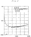
- Fig. 1 illustrates the results of measurement of electromagnetic waves by the advantest method.
- a shielding effect similar to that obtained with an electroless plating (Cu) film having a thickness of 1.3 ⁇ m as shown in Fig. 3 is observed.
- even a thin thickness as 0.6 ⁇ m for Cu and 0.1 ⁇ m for Sn gives a satisfactory effect, thus contributing to a saving of resources.
- a film was formed by high-frequency excited plasma (13.56 MHz) directly in a vacuum chamber on a 150 x 150 mm and 3 mm-thick injection molding sample comprising ABS/PC (50/50) resin, without conducting washing and without providing a primer coat layer.
- Plasma was held for ten minutes, and immediately a film was formed under 1 x 10 -4 Torr to a thickness of 0.1 ⁇ m. Then after holding plasma for two minutes, a 0.2 ⁇ m tin film was formed under 1.5 x 10 -4 Torr.
- Test item Test method Evaluation Adhesion test conformity to ASTMD3359-7B Class 5B Humidity resistance 65°C ⁇ 95% RH ⁇ 240hr Adhesion class 5B Resistance value 5.7mm ⁇ (No change between before and after the test) Pencil hardness Japan Industrial Standard K5401 3 H Salt spray test Japan Industrial Standard Z2371 Adhesion class 5B 5 % NaCl atmosphere 35°C Sample angle: 45°, Spray for 8 hrs., stoppage for 16 hrs., Repeating six such cycles Resistance value 6.1mm ⁇ (No change between before and after the test)
- an electromagnetic wave shielding plastic molding having similarly excellent properties was obtained by using an ABS (DIAPET 3001M) molding.
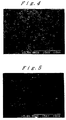
- Fig. 4 is an electron micrograph illustrating a surface etched by bombardment, and Fig. 5,1 a non-bombard-treated surface.
- the surface is etched by high-frequency excited plasma bombardment, and achievement of a high adhering strength was confirmed, by the anchor effect of the adhering thin film.
- a copper film and a nickel-chromium film were formed directly by high-frequency excited plasma on a 150 x 150 x 3.0 mm ABS sheet without washing and without providing a primer coat layer.
- the ABS sheet was held for ten minutes for bombardment in glow plasma generated by coil-shaped high-frequency excitation (13.56 MHz) electrodes by bringing the reached degree of vacuum to 2 x 10 -5 Torr and introducing argon under a partial pressure of 1 x 10 -3 Torr, and then immediately a 0.6 ⁇ m-thick copper film under 1.5 x 10 -4 Torr.
- nickel/chromium 80/20
- the thus obtained electromagnetic shielding plastic molding had the following excellent properties as shown in Table 5.
- a film was formed by high-frequency excited plasma (13.56 MHz) directly in vacuum chamber on a 1.50 x 150 mm and 3 mm-thick injection molding sample comprising ABS/PC (50/50) resin, without washing and without providing a primer coat layer.
- an electromagnetic wave shielding plastic molding which is excellent in the electromagnetic wave shielding effects, while displaying favorable features of a gas-phase deposited film, permits savings in resources, has a high film adhering strength, is free from production of decoloration or rustle, does not require washing nor provision of a primer coat layer, and eliminates the fear of contamination by waste liquid or waste gases.
- a copper film and a nickel film were formed directly by high-frequency excited plasma on 150 x 150 x 3.0 mm ABS sheet without washing and without providing a primer coat layer.
- argon was introduced under a partial pressure of 1 x 10 -3 Torr, in the same vacuum chamber.
- Glow plasma produced by coil-shaped high-frequency excitation (13.56 MHz) electrodes was held for ten minutes, and then immediately, a 0.6 ⁇ m-thick copper film was formed under 1 x 10 -4 Torr.
- the film was held in plasma for two minutes, and immediately, a 0.2 ⁇ m-thick tin film was formed in an ethylene atmosphere of 1.5 x 10 -4 Torr.
- the thus obtained electromagnetic wave shielding plastic molding had excellent properties as shown in Table 6.
- the obtained plastic molding in the shape of a 100 x 100 x 1 mm sheet was placed on an iron plate, and a 1-pound steel ball was dropped from above at a distance of 1 m wherein the production of cracks was observed on the film.
- a film was formed by high-frequency excited plasma (13.56 MHz) directly in a vacuum chamber on a 150 x 150 and 3 mm-thick injection molding sample comprising ABS/PC (50/50) resin, without washing and without providing a primer coat layer.
- a 1.0 ⁇ m-thick copper film was formed under 1 x 10 -4 Torr.
- a 0.2 ⁇ m-thick nickel-chromium alloy film at a ratio of Ni to Cr of 60:40 was formed in ethylene atmosphere under 1.6 x 10 -4 Torr.
- An electromagnetic wave shielding plastic molding is implemented, which is excellent in electromagnetic shielding effect, has a high adhering strength, is excellent in corrosion resistance and heat shock resistance, and is satisfactory both in strength and flexibility.
- a copper film and an SnO 2 film were formed by high-frequency excited plasma on the inner bottom surface of an ABS container molding having inside dimensions of 50 x 50 x 501, without washing and without providing a primer coat layer.
- the reached degree of vacuum was brought to 3 x 10 -5 Torr, and argon was introduced under a partial pressure of 1 x 10 -3 Torr.
- argon was introduced under a partial pressure of 1 x 10 -3 Torr.
- glow plasma generated by coil-shaped high-frequency excitation (13.56 MHz) electrodes a 1 ⁇ m-thick copper film was formed under 1 x 10 -4 Torr.
- the thus obtained electromagnetic wave shielding plastic molding had excellent properties as shown in Table 7.
- Test item Test method Evaluation Adhesion test conformity to ASTMD3359-7B Class 5B Humidity resistance 65°C ⁇ 95% RH ⁇ 240hr Adhesion class 5 B Resistance value 5.5mm ⁇ (No change between before and after the test) Pencil hardness Japan Industrial Standard K5401 3 H Salt spray test Japan Industrial Standard Z2371 Adhesion class 5 B 5 % NaCl atmosphere 35°C Sample angle: 45°, Spray for 8 hrs., stoppage for 16 hrs., Repeating six such cycles Resistance value 5.8mm ⁇ (No change between before and after the test)
- a film was formed by high-frequency excited plasma (13.56 MHz) directly in a vacuum chamber on a 150 x 150 and 3 mm-thick injection molding sample comprising an ABS/PC (50/50) resin, without washing and without providing a primer coat layer.
- the vacuum was brought to 3 x 10 -5 Torr, and argon was introduced so as to achieve 1 x 10 -3 Torr.
- a 1.0 ⁇ m-thick copper film was formed under 1 x 10 -4 Torr. Then, after molding plasma further for two minutes, a 0.2 ⁇ m-thick ITO film was formed under an oxygen partial pressure of 1.5 x 10 -4 Torr.
- a copper film was formed directly by high-frequency excited plasma on the housing of an automotive moving telephone formed from an ABS-PC alloy material as a plastic injection molding, without washing and without providing a primer coat layer.
- the reached degree of vacuum was brought to 5 x 10 -5 Torr, and argon was introduced under a partial pressure of 2 x 10 -4 Torr.
- argon was introduced under a partial pressure of 2 x 10 -4 Torr.
- the thus obtained electromagnetic wave shielding plastic molding had very excellent properties as shown in Table 8.
- Test item Test method Evaluation Adhesion test conformity to ASTMD3359-7B Class 5B Humidity resistance 65°C ⁇ 95% RH ⁇ 240hr Adhesion class 5 B Resistance value 5.5mm ⁇ (No change between before and after the test) Pencil hardness Japan Industrial Standard K5401 3 H Salt spray test Japan Industrial Standard Z2371 Adhesion class 5 B 5 % NaCl atmosphere 35°C Sample angle: 45°, Spray for 8 hrs., stoppage for 16 hrs., Repeating six such cycles Resistance value 6.0mm ⁇ (No change between before and after the test)
- a 1 ⁇ m-thick copper film was formed by high-frequency excited plasma, directly in a vacuum chamber, on a 200 x 300 mm and 3mm-thick infection molding sample comprising an ABS resin, without washing and without providing a primer coat layer.
- Copper was vaporized by electron beam.
- the vacuum was brought to 4 x 10 -5 Torr, with an argon partial pressure of 4 x 10 -4 Torr.
- electrolytic plating was applied to a thickness of 5 ⁇ m, and an electromagnetic wave shielding plastic molding having excellent properties was obtained.
- Example 14 Under the same conditions as in the Example 14, a 3 ⁇ m-thick copper film was first formed, and then electrolytic copper plating was applied to a thickness of 10 ⁇ m.
- Test item Test method Evaluation Adhesion test conformity to ASTMD3359-7B Class 5B Humidity resistance 65°C ⁇ 95% RH ⁇ 240hr Adhesion class 5 B Resistance value 5.7mm ⁇ (No change between before and after the test) Pencil hardness Japan Industrial Standard K5401 3 H Salt spray test Japan Industrial Standard Z2371 Adhesion class 5 B 5 % NaCl atmosphere 35°C Sample angle: 45°, Spray for 8 hrs., stoppage for 16 hrs., Repeating six such cycles Resistance value 6.1mm ⁇ (No change between before and after the test)
- a water-soluble paint comprising an acrylic emulsion paint was applied, and the product was dried by hot blast for 60 minutes at a temperature of 85°C. A 1.5 ⁇ m-thick primer coat layer was thus formed.
- a vacuum deposition chamber In a vacuum deposition chamber, the vacuum was brought to 3 x 10 -5 Torr, and argon was introduced under a partial pressure of 1 x 10 -4 Torr. Immediately after holding for five minutes in glow plasma generated by coil-shaped high-frequency excitation (13.56 MHz) electrodes, a 2.0 ⁇ m-thick aluminum film was formed under an argon partial pressure of 2 x 10 -4 Torr.
- the film was excellent in adhering strength, corrosion resistance, water resistance, and heat shock resistance.
- An acrylic emulsion paint was applied onto a shielding plate of a portable telephone formed with a polycarbonate (PC) molding material containing 8 wt.% blended carbon fiber, and after hot blast drying at 80 °C for 60 minutes, a 20 ⁇ m-thick primer coat layer wag formed.
- PC polycarbonate
- the product was held for six minutes in a high-frequency plasma (13.56 MHz) under an argon pressure of 7 x 10 -4 Torr, and a 1 ⁇ m-thick copper film was formed under an argon pressure of 2 x 10⁻⁴ Torr. Immediately after that, a 0.2 ⁇ m-thick nickel film was formed.
- This Example was carried out under the same conditions as in the Example 2, previously washing before the bombard-treatment was employed.
- a sliding oil adhered to the parts of the surface is completely removed by the washing-treatment.
- the adhesion properties of the conductive layer to the parts of the surface above-mentioned was more excellent. Indeed, the ratio of sub-standard articles, from the view point of the adhesion of the conductive layer, decreases from 1 % to 0.3 %.
Description
4) A method of manufacturing an electromagnetic wave shielding plastic molding, which comprises the steps of providing a primer coat layer comprising a water-soluble paint on the surface of a plastic molding containing a filler, and after drying same, providing a conductive layer comprising at least one metal selected from the group consisting of Al, Cu, Ni, Cr and Sn or an alloy thereof by high-frequency excited plasma in a vacuum chamber.
5) A method of manufacturing an electromagnetic wave shielding plastic molding, which comprises the step of previously washing parts of the surface of a plastic molding. which are contacted by molding pins or sliding cores having a sliding oil at the surface thereof, using an organic solvent, followed by bombard-treating the surface of plastic molding with a high-frequency plasma, and then providing a conductive layer by high-frequency excited plasma on the surface of a plastic molding.
| Test item | Test method | Evaluation |
| Adhesion test | conformity to ASTMD3359-7B | Class 5B |
| Humidity resistance | 65°C × 95% RH × 240hr | Adhesion class 5B |
| Resistance value 7.0mm Ω | ||
| (No change between before and after the test) | ||
| Pencil hardness | Japan Industrial Standard K5401 | 3 H |
| Salt spray test | Japan Industrial Standard Z2371 | Adhesion class 5B |
| 5 % NaCl atmosphere 35°C Sample angle: 45°, Spray for 8 hrs., stoppage for 16 hrs., Repeating six such cycles | Resistance value 7.0mm Ω | |
| (No change between before and after the test) |
| Test item | Test method | Evaluation |
| Adhesion test | conformity to ASTMD3359-7B | Class 5B |
| Humidity resistance | 65°C × 95% RH × 240hr | Adhesion class 5B |
| Resistance value 6.8mm Ω | ||
| (No change between before and after the test) | ||
| Pencil hardness | Japan Industrial Standard K5401 | 3 H |
| Salt spray test | Japan Industrial Standard Z2371 | Adhesion class 5B |
| 5 % NaCl atmosphere 35°C Sample angle: 45°, Spray for 8 hrs., stoppage for 16 hrs., Repeating six such cycles | Resistance value 6.8mm Ω | |
| (No change between before and after the test) |
| Test item | Test method | Evaluation |
| Adhesion test | conformity to ASTMD3359-7B | Class 5B |
| Humidity resistance | 65°C × 95% RH × 240hr | Adhesion class 5B |
| Resistance value 5.5mm Ω | ||
| (No change between before and after the test) | ||
| Pencil hardness | Japan Industrial Standard K5401 | 3 H |
| Salt spray test | Japan Industrial Standard Z2371 | Adhesion class 5B |
| 5 % NaCl atmosphere 35°C Sample angle: 45°, Spray for 8 hrs., stoppage for 16 hrs., Repeating six such cycles | Resistance value 6.0mm Ω | |
| (No change between before and after the test) |
| Test item | Test method | Evaluation |
| Adhesion test | conformity to ASTMD3359-7B | Class 5B |
| Humidity resistance | 65°C × 95% RH × 240hr | Adhesion class 5B |
| Resistance value 5.7mm Ω | ||
| (No change between before and after the test) | ||
| Pencil hardness | Japan Industrial Standard K5401 | 3 H |
| Salt spray test | Japan Industrial Standard Z2371 | Adhesion class 5B |
| 5 % NaCl atmosphere 35°C Sample angle: 45°, Spray for 8 hrs., stoppage for 16 hrs., Repeating six such cycles | Resistance value 6.1mm Ω | |
| (No change between before and after the test) |
| Test item | Test method | Evaluation |
| Adhesion test | conformity to ASTMD3359-7B | Class 5B |
| Humidity resistance | 65°C × 95% RH × 240hr | Adhesion class 5 B |
| Resistance value 5.5mm Ω | ||
| (No change between before and after the test) | ||
| Pencil hardness | Japan Industrial Standard K5401 | 3 H |
| Salt spray test | Japan Industrial Standard Z2371 | Adhesion class 5 B |
| 5 % NaCl atmosphere 35°C Sample angle: 45°, Spray for 8 hrs., stoppage for 16 hrs., Repeating six such cycles | Resistance value 5.6mm Ω | |
| (No change between before and after the test) |
| Test item | Test method | Evaluation |
| Adhesion test | conformity to ASTMD3359-7B | Class 5B |
| Humidity resistance | 65°C × 95% RH × 240hr | Adhesion class 5 B |
| Resistance value 5.4mm Ω | ||
| (No change between before and after the test) | ||
| Pencil hardness | Japan Industrial Standard K5401 | 3 H |
| Salt spray test | Japan Industrial Standard Z2371 | Adhesion class 5 B |
| 5 % NaCl atmosphere 35°C Sample angle: 45°, Spray for 8 hrs., stoppage for 16 hrs., Repeating six such cycles | Resistance value 5.5mm Ω | |
| (No change between before and after the test) |
| Test item | Test method | Evaluation |
| Adhesion test | conformity to ASTMD3359-7B | Class 5B |
| Humidity resistance | 65°C × 95% RH × 240hr | Adhesion class 5 B |
| Resistance value 5.5mm Ω | ||
| (No change between before and after the test) | ||
| Pencil hardness | Japan Industrial Standard K5401 | 3 H |
| Salt spray test | Japan Industrial Standard Z2371 | Adhesion class 5 B |
| 5 % NaCl atmosphere 35°C Sample angle: 45°, Spray for 8 hrs., stoppage for 16 hrs., Repeating six such cycles | Resistance value 5.8mm Ω | |
| (No change between before and after the test) |
| Test item | Test method | Evaluation |
| Adhesion test | conformity to ASTMD3359-7B | Class 5B |
| Humidity resistance | 65°C × 95% RH × 240hr | Adhesion class 5 B |
| Resistance value 5.5mm Ω | ||
| (No change between before and after the test) | ||
| Pencil hardness | Japan Industrial Standard K5401 | 3 H |
| Salt spray test | Japan Industrial Standard Z2371 | Adhesion class 5 B |
| 5 % NaCl atmosphere 35°C Sample angle: 45°, Spray for 8 hrs., stoppage for 16 hrs., Repeating six such cycles | Resistance value 6.0mm Ω | |
| (No change between before and after the test) |
| Test item | Test method | Evaluation |
| Adhesion test | conformity to ASTMD3359-7B | Class 5B |
| Humidity resistance | 65°C × 95% RH × 240hr | Adhesion class 5 B |
| Resistance value 5.7mm Ω | ||
| (No change between before and after the test) | ||
| Pencil hardness | Japan Industrial Standard K5401 | 3 H |
| Salt spray test | Japan Industrial Standard Z2371 | Adhesion class 5 B |
| 5 % NaCl atmosphere 35°C Sample angle: 45°, Spray for 8 hrs., stoppage for 16 hrs., Repeating six such cycles | Resistance value 6.1mm Ω | |
| (No change between before and after the test) |
Claims (21)
- A method of manufacturing an electromagnetic wave shielding plastic molding, which comprises the step of providing a conductive layer comprising at least a metal selected from the group consisting of Al, Cu, Ni, Cr and Sn or an alloy thereof by high-frequency excited plasma on the surface of a plastic molding, without prior washing and without providing a primer layer.
- A method of manufacturing an electromagnetic wave shielding plastic molding as claimed in Claim 1, wherein said conductive layer comprises a single layer or multiple layers.
- A method of manufacturing an electromagnetic wave shielding plastic molding as claimed in Claim 1 or Claim 2, wherein after bombardment by high-frequency excited plasma, the conductive layer is provided by high-frequency excited plasma.
- A method of manufacturing an electromagnetic wave shielding plastic molding as claimed in any one of the preceding claims, wherein, without prior washing and without providing a primer coat layer, an aluminium film having a thickness of from 0.7 to 5.0 µm is formed by high-frequency excited plasma on the surface of the plastic molding.
- A method of manufacturing an electromagnetic wave shielding plastic molding as claimed in any one of claims 1 to 4, wherein, without prior washing and without providing a primer coat layer, a copper film having a thickness of from 0.7 to 5.0 µm and an aluminum film are formed by high-frequency excited plasma on the surface of the plastic molding.
- A method of manufacturing an electromagnetic wave shielding plastic molding as claimed in any one of claims 1 to 3, wherein without prior washing and without providing a primer coat layer, a copper film having a thickness of 0.7 to 5.0 µm is formed in advance by high-frequency excited plasma in the same vacuum tank on the surface of the plastic molding, and then a tin film having a thickness of from 0.05 to 2.0 µm is formed by high-frequency excited plasma.
- A method of manufacturing an electromagnetic wave shielding plastic molding as claimed in any one of claims 1 to 3, wherein without prior washing and without providing a primer coat layer, a copper film having a thickness of from 0.7 to 5.0 µm is formed in advance by high-frequency excited plasma in the same vacuum tank on the surface of the plastic molding, and then a nickel-chromium film having a thickness of from 0.05 to 2.0 µm and a nickel/chromium ratio of 50-80:50-20 is formed by high-frequency excited plasma.
- A method of manufacturing an electromagnetic wave shielding plastic molding as claimed in any one of claims 1 to 3, wherein without prior washing and without providing a primer coat layer, a copper film having a thickness of from 0.7 to 5.0 µm is formed in advance by high-frequency excited plasma in the same vacuum tank on the surface of the plastic molding, and then a metal or alloy film having a thickness of from 0.05 to 2.0 µm is formed in an organic gas atmosphere by high-frequency excited plasma.
- A method of manufacturing an electromagnetic wave shielding plastic molding as claimed in any one of claims 1 to 3, wherein without prior washing and without providing a primer coat layer, a copper film having a thickness of from 0.7 to 5.0 µm is formed in advance by high-frequency excited plasma in the same vacuum tank on the surface of the plastic molding, and then a conductive oxide film having a thickness of from 0.05 to 2.0 µm is formed by high-frequency excited plasma.
- A method of manufacturing an electromagnetic wave shielding plastic molding as claimed in any one of claims 1 to 3, wherein without prior washing and without providing a primer coat layer, a copper film having a thickness of from 0.7 to 5.0 µm is formed in advance by high-frequency excited plasma in the same vacuum tank on the surface of the plastic molding, and then a copper electrolytic plating film having a thickness of from 10 to 30 µm is formed.
- A method of manufacturing an electromagnetic wave shielding plastic molding as claimed in Claim 10, wherein a protecting film is formed on said copper electrolytic plating film.
- A method of manufacturing an electromagnetic wave shielding plastic molding, which comprises the steps of providing a primer coat layer comprising a water-soluble paint on the surface of a plastic molding containing a filler, and after drying, providing a conductive layer comprising at least a metal selected from the group consisting of Al, Cu, Ni. Cr and Sn and alloys thereof by high-frequency excited plasma in a vacuum tank.
- A method of manufacturing an electromagnetic wave shielding plastic molding as claimed in Claim 12, wherein said conductive layer comprises a single layer or multiple films.
- A method of manufacturing an electromagnetic wave shielding plastic molding as claimed in Claim 12 or Claim 13, wherein a primer coat layer comprising a water-soluble paint and having a thickness of from 1 to 30 µm is formed on the surface of the plastic molding containing a filler, and after low-temperature drying at a temperature of up to 100°C, an aluminum film having a thickness of from 0.6 to 5.0 µm is formed by high-frequency excited plasma in a vacuum tank.
- A method of manufacturing an electromagnetic wave shielding plastic molding as claimed in Claim 14, wherein a primer coat layer comprising a water-soluble paint and having a thickness of from 1 to 30 µm is formed on the surface of the plastic molding containing a filler, then after low-temperature drying at a temperature of up to 100°C, a copper film having a thickness of from 0.7 to 5.0 µm is formed in advance by high-frequency excited plasma in the vacuum tank, and a corrosion-resistant metal or alloy film having a thickness of from 0.05 to 3.0 µm is further formed.
- A method of manufacturing an electromagnetic wave shielding plastic molding as claimed in Claim 15, wherein said corrosion-resistant metal or alloy film is formed in an organic gas atmosphere.
- A method of manufacturing an electromagnetic wave shielding plastic molding, which comprises the steps of previously washing parts of surface of a plastic molding, which are contacted by molding pins or sliding cores adhering a sliding oil at the surface thereof, using an organic solvent or organic solvents, followed by bombard-treating the surface of plastic molding with high-frequency plasma, and then providing a conductive layer comprising at least one selected from the group consisting of al, Cu, Ni, Cr and sn and alloys thereof by high-frequency excited plasma on the surface of a plastic molding.
- A method as claimed in claim 17, wherein the organic solvent has a low boiling points.
- A method as claimed in claim 17 or claim 18, wherein the organic solvent is selected from the group of ethanol, n-hexane and diethylether.
- A method of manufacturing an electromagnetic wave shielding plastic moulding, which comprises the step of providing said plastic moulding with a conductive layer comprising at least a metal selected from the group consisting of Al, Cu, Ni, Cr and Sn or an alloy thereof by high-frequency excited plasma deposition.
- A method of manufacturing an electromagnetic wave shielding plastic molding as claimed in any one of the preceding claims, wherein the conductive layer is formed by plasma excitation caused by the introduction of an inert gas under a partial pressure of about 1x10⁻⁴ to 1x10⁻³ Torr by the application of voltage from a high frequency power source in a vacuum tank having a degree of vacuum of 1x10⁻⁴ to 1x10⁻⁵ Torr.
Applications Claiming Priority (12)
| Application Number | Priority Date | Filing Date | Title |
|---|---|---|---|
| JP298940/92 | 1992-11-09 | ||
| JP4298940A JP2561992B2 (en) | 1992-11-09 | 1992-11-09 | Electromagnetic wave shield plastic molding |
| JP317380/92 | 1992-11-26 | ||
| JP4317380A JP2561993B2 (en) | 1992-11-26 | 1992-11-26 | Electromagnetic wave shield plastic molding |
| JP29216/93 | 1993-02-18 | ||
| JP29217/93 | 1993-02-18 | ||
| JP2921593A JPH06240034A (en) | 1993-02-18 | 1993-02-18 | Electromagnetic-wave-shielding molded plastic article |
| JP29215/93 | 1993-02-18 | ||
| JP5029216A JPH06240027A (en) | 1993-02-18 | 1993-02-18 | Electromagnetic-wave-shielding plastic molding |
| JP2921793A JPH06240035A (en) | 1993-02-18 | 1993-02-18 | Electromagnetic-wave-shielding molded plastic article |
| JP22263893A JPH0770345A (en) | 1993-09-07 | 1993-09-07 | Electromagnetic shielded plastic molding |
| JP222638/93 | 1993-09-07 |
Publications (2)
| Publication Number | Publication Date |
|---|---|
| EP0597670A1 EP0597670A1 (en) | 1994-05-18 |
| EP0597670B1 true EP0597670B1 (en) | 1998-02-18 |
Family
ID=27549444
Family Applications (1)
| Application Number | Title | Priority Date | Filing Date |
|---|---|---|---|
| EP93308934A Expired - Lifetime EP0597670B1 (en) | 1992-11-09 | 1993-11-09 | Method of manufacturing electromagnetic wave shielding plastic molding |
Country Status (3)
| Country | Link |
|---|---|
| US (1) | US5462771A (en) |
| EP (1) | EP0597670B1 (en) |
| DE (1) | DE69317035T2 (en) |
Families Citing this family (22)
| Publication number | Priority date | Publication date | Assignee | Title |
|---|---|---|---|---|
| US5385785A (en) * | 1993-08-27 | 1995-01-31 | Tapeswitch Corporation Of America | Apparatus and method for providing high temperature conductive-resistant coating, medium and articles |
| DE19617656A1 (en) * | 1996-05-03 | 1997-11-06 | Siegfried Schaal Metallveredel | Shielding molding for electronic components |
| US5989720A (en) * | 1996-12-25 | 1999-11-23 | Taniyama & Co., Ltd. | Electromagnetic wave shield material composition and electromagnetic wave shield product including such material composition |
| NL1008197C2 (en) * | 1998-02-04 | 1999-08-05 | Stork Screens Bv | Method for manufacturing a carrier with a shielding for interference radiation, as well as a shielding material. |
| JP3456473B2 (en) | 2000-11-16 | 2003-10-14 | 日本電気株式会社 | Mobile phone case |
| US6562414B2 (en) | 2001-10-10 | 2003-05-13 | Sport Court, Inc. | Method of coating polyolefin floor tile |
| US20040058089A1 (en) * | 2001-10-10 | 2004-03-25 | Sport Court, Inc. | Floor tile coating method and system |
| TWI276397B (en) * | 2003-03-21 | 2007-03-11 | Hon Hai Prec Ind Co Ltd | EMI-shielding assembly and method for the manufacture of same |
| US7748177B2 (en) | 2004-02-25 | 2010-07-06 | Connor Sport Court International, Inc. | Modular tile with controlled deflection |
| US7849642B2 (en) | 2004-03-12 | 2010-12-14 | Connor Sport Court International, Inc. | Tile with wide coupling configuration and method for the same |
| US8397466B2 (en) | 2004-10-06 | 2013-03-19 | Connor Sport Court International, Llc | Tile with multiple-level surface |
| US8407951B2 (en) | 2004-10-06 | 2013-04-02 | Connor Sport Court International, Llc | Modular synthetic floor tile configured for enhanced performance |
| USD656250S1 (en) | 2005-03-11 | 2012-03-20 | Connor Sport Court International, Llc | Tile with wide mouth coupling |
| KR100761435B1 (en) * | 2006-12-19 | 2007-09-27 | 구자은 | Electromagnetic wave shield with vacuum deposited metal using water dispersed polyurethane |
| US8502684B2 (en) | 2006-12-22 | 2013-08-06 | Geoffrey J. Bunza | Sensors and systems for detecting environmental conditions or changes |
| US7812731B2 (en) * | 2006-12-22 | 2010-10-12 | Vigilan, Incorporated | Sensors and systems for detecting environmental conditions or changes |
| CN101262748B (en) * | 2007-03-07 | 2012-05-30 | 鸿富锦精密工业(深圳)有限公司 | Shaped inlay part and its making method |
| ITGE20070053A1 (en) * | 2007-06-15 | 2008-12-16 | Nantech S R L | KEYCHAIN OR SIMILAR CHANNEL, AND METHOD FOR ITS MANUFACTURE |
| KR101375956B1 (en) * | 2012-07-05 | 2014-03-18 | 엘에스산전 주식회사 | Electronic component box for vehicle |
| CN111441018A (en) * | 2015-10-10 | 2020-07-24 | 江苏新思达电子有限公司 | Method for electroplating electromagnetic radiation-proof layer on plastic |
| JP2017212274A (en) * | 2016-05-24 | 2017-11-30 | タツタ電線株式会社 | Electromagnetic wave shielding film and shielded printed wiring board including the same |
| KR102617428B1 (en) * | 2023-03-17 | 2023-12-27 | 주식회사 크레토즈 | Method of manufacturing plastic-based article, injection mold for manufacturing plastic-based article, injection mold set for manufacturing plastic-based article, and plastic-based article |
Family Cites Families (6)
| Publication number | Priority date | Publication date | Assignee | Title |
|---|---|---|---|---|
| US4605565A (en) * | 1982-12-09 | 1986-08-12 | Energy Conversion Devices, Inc. | Method of depositing a highly conductive, highly transmissive film |
| US4544571A (en) | 1984-02-13 | 1985-10-01 | Pennwalt Corporation | Method of manufacture of EMI/RFI vapor deposited composite shielding panel |
| US4534921A (en) * | 1984-03-06 | 1985-08-13 | Asm Fico Tooling, B.V. | Method and apparatus for mold cleaning by reverse sputtering |
| DE3510982A1 (en) | 1985-03-22 | 1986-09-25 | Schering AG, Berlin und Bergkamen, 1000 Berlin | MANUFACTURE OF METALLIC STRUCTURES ON NON-CONDUCTORS |
| DE3744062A1 (en) | 1987-12-22 | 1989-07-13 | Schering Ag | METHOD FOR THE PRODUCTION OF ADHESIVE METALLIC STRUCTURES ON FLUORINE POLYMERS AND THERMOPLASTIC PLASTICS |
| FR2682688B1 (en) * | 1991-10-22 | 1994-01-14 | Thomson Csf | PROCESS FOR THE METALLIZATION OF THE SURFACE OF PARTS OF PLASTIC MATERIAL AND PARTS FOR ELECTRONIC USE THUS OBTAINED. |
-
1993
- 1993-11-09 US US08/149,533 patent/US5462771A/en not_active Expired - Lifetime
- 1993-11-09 EP EP93308934A patent/EP0597670B1/en not_active Expired - Lifetime
- 1993-11-09 DE DE69317035T patent/DE69317035T2/en not_active Expired - Lifetime
Also Published As
| Publication number | Publication date |
|---|---|
| US5462771A (en) | 1995-10-31 |
| DE69317035T2 (en) | 1998-06-10 |
| EP0597670A1 (en) | 1994-05-18 |
| DE69317035D1 (en) | 1998-03-26 |
Similar Documents
| Publication | Publication Date | Title |
|---|---|---|
| EP0597670B1 (en) | Method of manufacturing electromagnetic wave shielding plastic molding | |
| KR900004543B1 (en) | Rfi shielded plastic articles and process for making same | |
| US20050106403A1 (en) | Shaped metal article and method of producing shaped metal article having oxide coating | |
| JPH0770345A (en) | Electromagnetic shielded plastic molding | |
| PL103465B1 (en) | LAMINATE ON A POLYMERIC SUBSTRATE | |
| US5198096A (en) | Method of preparing polycarbonate surfaces for subsequent plating thereon and improved metal-plated plastic articles made therefrom | |
| Kupfer et al. | Plasma and ion beam assisted metallization of polymers and their application | |
| JPS61210183A (en) | Method for providing metal film to surface of polymer | |
| CN102792786B (en) | 2 layers of flexible substrate and manufacture method thereof | |
| JP3290389B2 (en) | Surface coatings for insulating materials, methods of obtaining them, and applications in the protection of insulating containers | |
| Kupfer et al. | Ecologically important metallization processes for high-performance polymers | |
| CN1234910C (en) | Technique for producing multifunctional aluminum base flexible shielding material | |
| JP2817891B2 (en) | Manufacturing method of electromagnetic wave shielding plastic molded products | |
| Fessmann et al. | Adherent metallization of carbon-fibre-reinforced plastic composites using a combined vacuum/electrochemical deposition process | |
| EP0470610B1 (en) | Synthetic resin molded article having metallic thin film on the surface thereof | |
| KR100438641B1 (en) | Resin composition for metal deposition without electricity and metal deposition method without electricity | |
| JP2561992B2 (en) | Electromagnetic wave shield plastic molding | |
| KR100431248B1 (en) | Plating Method on A Nonconductor Using Conductive Polymer Composition | |
| JP2561993B2 (en) | Electromagnetic wave shield plastic molding | |
| KR100395794B1 (en) | LAYERED STRUCTURE OF THIN FILMS INCLUDING Ag FILM FOR PROVIDING HIGH RELIABILITY ON INSULATING SUBSTRATE AND METHOD FOR FABRICATING THEREOF | |
| JPH06240027A (en) | Electromagnetic-wave-shielding plastic molding | |
| JP3775273B2 (en) | Electromagnetic shielding film | |
| JPH06240034A (en) | Electromagnetic-wave-shielding molded plastic article | |
| KR20110072767A (en) | A method for preparing a electromagnetic interference film | |
| JPH06240035A (en) | Electromagnetic-wave-shielding molded plastic article |
Legal Events
| Date | Code | Title | Description |
|---|---|---|---|
| PUAI | Public reference made under article 153(3) epc to a published international application that has entered the european phase |
Free format text: ORIGINAL CODE: 0009012 |
|
| AK | Designated contracting states |
Kind code of ref document: A1 Designated state(s): DE FR GB |
|
| 17P | Request for examination filed |
Effective date: 19940906 |
|
| GRAG | Despatch of communication of intention to grant |
Free format text: ORIGINAL CODE: EPIDOS AGRA |
|
| 17Q | First examination report despatched |
Effective date: 19951218 |
|
| GRAG | Despatch of communication of intention to grant |
Free format text: ORIGINAL CODE: EPIDOS AGRA |
|
| GRAH | Despatch of communication of intention to grant a patent |
Free format text: ORIGINAL CODE: EPIDOS IGRA |
|
| GRAH | Despatch of communication of intention to grant a patent |
Free format text: ORIGINAL CODE: EPIDOS IGRA |
|
| GRAA | (expected) grant |
Free format text: ORIGINAL CODE: 0009210 |
|
| AK | Designated contracting states |
Kind code of ref document: B1 Designated state(s): DE FR GB |
|
| REF | Corresponds to: |
Ref document number: 69317035 Country of ref document: DE Date of ref document: 19980326 |
|
| ET | Fr: translation filed | ||
| PLBE | No opposition filed within time limit |
Free format text: ORIGINAL CODE: 0009261 |
|
| STAA | Information on the status of an ep patent application or granted ep patent |
Free format text: STATUS: NO OPPOSITION FILED WITHIN TIME LIMIT |
|
| 26N | No opposition filed | ||
| REG | Reference to a national code |
Ref country code: FR Ref legal event code: CD Ref country code: FR Ref legal event code: CA |
|
| REG | Reference to a national code |
Ref country code: GB Ref legal event code: IF02 |
|
| REG | Reference to a national code |
Ref country code: FR Ref legal event code: TQ |
|
| PGFP | Annual fee paid to national office [announced via postgrant information from national office to epo] |
Ref country code: DE Payment date: 20101124 Year of fee payment: 18 |
|
| PGFP | Annual fee paid to national office [announced via postgrant information from national office to epo] |
Ref country code: GB Payment date: 20101101 Year of fee payment: 18 |
|
| PGFP | Annual fee paid to national office [announced via postgrant information from national office to epo] |
Ref country code: FR Payment date: 20111018 Year of fee payment: 19 |
|
| GBPC | Gb: european patent ceased through non-payment of renewal fee |
Effective date: 20121109 |
|
| REG | Reference to a national code |
Ref country code: FR Ref legal event code: ST Effective date: 20130731 |
|
| REG | Reference to a national code |
Ref country code: DE Ref legal event code: R119 Ref document number: 69317035 Country of ref document: DE Effective date: 20130601 |
|
| PG25 | Lapsed in a contracting state [announced via postgrant information from national office to epo] |
Ref country code: DE Free format text: LAPSE BECAUSE OF NON-PAYMENT OF DUE FEES Effective date: 20130601 |
|
| PG25 | Lapsed in a contracting state [announced via postgrant information from national office to epo] |
Ref country code: FR Free format text: LAPSE BECAUSE OF NON-PAYMENT OF DUE FEES Effective date: 20121130 Ref country code: GB Free format text: LAPSE BECAUSE OF NON-PAYMENT OF DUE FEES Effective date: 20121109 |