EP0594441B1 - Semiconductor device - Google Patents
Semiconductor device Download PDFInfo
- Publication number
- EP0594441B1 EP0594441B1 EP93308403A EP93308403A EP0594441B1 EP 0594441 B1 EP0594441 B1 EP 0594441B1 EP 93308403 A EP93308403 A EP 93308403A EP 93308403 A EP93308403 A EP 93308403A EP 0594441 B1 EP0594441 B1 EP 0594441B1
- Authority
- EP
- European Patent Office
- Prior art keywords
- layer
- crystal silicon
- substrate
- film
- semiconductor device
- Prior art date
- Legal status (The legal status is an assumption and is not a legal conclusion. Google has not performed a legal analysis and makes no representation as to the accuracy of the status listed.)
- Expired - Lifetime
Links
Images


Classifications
-
- G—PHYSICS
- G02—OPTICS
- G02F—OPTICAL DEVICES OR ARRANGEMENTS FOR THE CONTROL OF LIGHT BY MODIFICATION OF THE OPTICAL PROPERTIES OF THE MEDIA OF THE ELEMENTS INVOLVED THEREIN; NON-LINEAR OPTICS; FREQUENCY-CHANGING OF LIGHT; OPTICAL LOGIC ELEMENTS; OPTICAL ANALOGUE/DIGITAL CONVERTERS
- G02F1/00—Devices or arrangements for the control of the intensity, colour, phase, polarisation or direction of light arriving from an independent light source, e.g. switching, gating or modulating; Non-linear optics
- G02F1/01—Devices or arrangements for the control of the intensity, colour, phase, polarisation or direction of light arriving from an independent light source, e.g. switching, gating or modulating; Non-linear optics for the control of the intensity, phase, polarisation or colour
- G02F1/13—Devices or arrangements for the control of the intensity, colour, phase, polarisation or direction of light arriving from an independent light source, e.g. switching, gating or modulating; Non-linear optics for the control of the intensity, phase, polarisation or colour based on liquid crystals, e.g. single liquid crystal display cells
- G02F1/133—Constructional arrangements; Operation of liquid crystal cells; Circuit arrangements
- G02F1/1333—Constructional arrangements; Manufacturing methods
- G02F1/1345—Conductors connecting electrodes to cell terminals
- G02F1/13454—Drivers integrated on the active matrix substrate
-
- H—ELECTRICITY
- H01—ELECTRIC ELEMENTS
- H01L—SEMICONDUCTOR DEVICES NOT COVERED BY CLASS H10
- H01L23/00—Details of semiconductor or other solid state devices
- H01L23/34—Arrangements for cooling, heating, ventilating or temperature compensation ; Temperature sensing arrangements
- H01L23/36—Selection of materials, or shaping, to facilitate cooling or heating, e.g. heatsinks
- H01L23/367—Cooling facilitated by shape of device
-
- H—ELECTRICITY
- H01—ELECTRIC ELEMENTS
- H01L—SEMICONDUCTOR DEVICES NOT COVERED BY CLASS H10
- H01L27/00—Devices consisting of a plurality of semiconductor or other solid-state components formed in or on a common substrate
- H01L27/02—Devices consisting of a plurality of semiconductor or other solid-state components formed in or on a common substrate including semiconductor components specially adapted for rectifying, oscillating, amplifying or switching and having at least one potential-jump barrier or surface barrier; including integrated passive circuit elements with at least one potential-jump barrier or surface barrier
- H01L27/12—Devices consisting of a plurality of semiconductor or other solid-state components formed in or on a common substrate including semiconductor components specially adapted for rectifying, oscillating, amplifying or switching and having at least one potential-jump barrier or surface barrier; including integrated passive circuit elements with at least one potential-jump barrier or surface barrier the substrate being other than a semiconductor body, e.g. an insulating body
- H01L27/1203—Devices consisting of a plurality of semiconductor or other solid-state components formed in or on a common substrate including semiconductor components specially adapted for rectifying, oscillating, amplifying or switching and having at least one potential-jump barrier or surface barrier; including integrated passive circuit elements with at least one potential-jump barrier or surface barrier the substrate being other than a semiconductor body, e.g. an insulating body the substrate comprising an insulating body on a semiconductor body, e.g. SOI
-
- G—PHYSICS
- G02—OPTICS
- G02F—OPTICAL DEVICES OR ARRANGEMENTS FOR THE CONTROL OF LIGHT BY MODIFICATION OF THE OPTICAL PROPERTIES OF THE MEDIA OF THE ELEMENTS INVOLVED THEREIN; NON-LINEAR OPTICS; FREQUENCY-CHANGING OF LIGHT; OPTICAL LOGIC ELEMENTS; OPTICAL ANALOGUE/DIGITAL CONVERTERS
- G02F1/00—Devices or arrangements for the control of the intensity, colour, phase, polarisation or direction of light arriving from an independent light source, e.g. switching, gating or modulating; Non-linear optics
- G02F1/01—Devices or arrangements for the control of the intensity, colour, phase, polarisation or direction of light arriving from an independent light source, e.g. switching, gating or modulating; Non-linear optics for the control of the intensity, phase, polarisation or colour
- G02F1/13—Devices or arrangements for the control of the intensity, colour, phase, polarisation or direction of light arriving from an independent light source, e.g. switching, gating or modulating; Non-linear optics for the control of the intensity, phase, polarisation or colour based on liquid crystals, e.g. single liquid crystal display cells
- G02F1/133—Constructional arrangements; Operation of liquid crystal cells; Circuit arrangements
- G02F1/1333—Constructional arrangements; Manufacturing methods
- G02F1/1335—Structural association of cells with optical devices, e.g. polarisers or reflectors
- G02F1/133509—Filters, e.g. light shielding masks
- G02F1/133512—Light shielding layers, e.g. black matrix
-
- G—PHYSICS
- G02—OPTICS
- G02F—OPTICAL DEVICES OR ARRANGEMENTS FOR THE CONTROL OF LIGHT BY MODIFICATION OF THE OPTICAL PROPERTIES OF THE MEDIA OF THE ELEMENTS INVOLVED THEREIN; NON-LINEAR OPTICS; FREQUENCY-CHANGING OF LIGHT; OPTICAL LOGIC ELEMENTS; OPTICAL ANALOGUE/DIGITAL CONVERTERS
- G02F1/00—Devices or arrangements for the control of the intensity, colour, phase, polarisation or direction of light arriving from an independent light source, e.g. switching, gating or modulating; Non-linear optics
- G02F1/01—Devices or arrangements for the control of the intensity, colour, phase, polarisation or direction of light arriving from an independent light source, e.g. switching, gating or modulating; Non-linear optics for the control of the intensity, phase, polarisation or colour
- G02F1/13—Devices or arrangements for the control of the intensity, colour, phase, polarisation or direction of light arriving from an independent light source, e.g. switching, gating or modulating; Non-linear optics for the control of the intensity, phase, polarisation or colour based on liquid crystals, e.g. single liquid crystal display cells
- G02F1/133—Constructional arrangements; Operation of liquid crystal cells; Circuit arrangements
- G02F1/136—Liquid crystal cells structurally associated with a semi-conducting layer or substrate, e.g. cells forming part of an integrated circuit
- G02F1/1362—Active matrix addressed cells
- G02F1/136277—Active matrix addressed cells formed on a semiconductor substrate, e.g. of silicon
- G02F1/136281—Active matrix addressed cells formed on a semiconductor substrate, e.g. of silicon having a transmissive semiconductor substrate
-
- H—ELECTRICITY
- H01—ELECTRIC ELEMENTS
- H01L—SEMICONDUCTOR DEVICES NOT COVERED BY CLASS H10
- H01L2924/00—Indexing scheme for arrangements or methods for connecting or disconnecting semiconductor or solid-state bodies as covered by H01L24/00
- H01L2924/0001—Technical content checked by a classifier
- H01L2924/0002—Not covered by any one of groups H01L24/00, H01L24/00 and H01L2224/00
-
- H—ELECTRICITY
- H01—ELECTRIC ELEMENTS
- H01L—SEMICONDUCTOR DEVICES NOT COVERED BY CLASS H10
- H01L2924/00—Indexing scheme for arrangements or methods for connecting or disconnecting semiconductor or solid-state bodies as covered by H01L24/00
- H01L2924/30—Technical effects
- H01L2924/301—Electrical effects
- H01L2924/3011—Impedance
Definitions
- the present invention relates to a semiconductor device. Moreover, the present invention relates to a substrate arrangement for driving a flat-plate light valve used for a direct-view display device and a projection-type display device.
- the present invention relates to a semiconductor integrated circuit substrate arrangement in which a group of picture element electrodes, a group of switches, and a group of driving circuit elements are formed on a single-crystal semiconductor silicon film on an electrical insulator.
- the substrate arrangement is integrated with, for example, a liquid crystal panel to constitute the so-called active-matrix arrangement.
- the present invention relates to a semiconductor device having a structure for minimising the generation of heat in the semiconductor device or preventing the temperature of the semiconductor device from rising by releasing the heat to the outside of the semiconductor device even if heat is generated.
- An existing active-matrix arrangement is made by forming amorphous silicon or polycrystal silicon on an electrical insulator as a transparent glass substrate or transparent quartz substrate and further forming some or all of a group of picture element electrodes, a group of switching elements, and a group of driving circuit elements on the amorphous or polycrystal silicon.
- an electrical insulator as a transparent glass substrate or transparent quartz substrate
- the semiconductor silicon on the electrical insulating film is called SOI (Silicon On Insulator), which is noted as a semiconductor device whose operation speed can be increased and whose integration density can be increased in recent years.
- SOI Silicon On Insulator
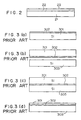
- Figure 2 shows a sectional view of a wafer made of the SOI.
- symbol 21 is a single-crystal silicon substrate with a thickness of 500 to 1,000 ⁇ m
- 22 is a silicon oxide film with a thickness of over 10 nm to several ⁇ m
- 23 is a single-crystal silicon film with a thickness of over 10 nm to several ⁇ m.
- the single-crystal silicon layer 23 on the electrical insulating film 22 is very thin. Therefore, when the integrated circuit comprises a complementary MIS transistor (complementary metal-insulator-semiconductor transistor; hereafter referred to as complementary MIS Tr), there are advantages such as the electrical capacities between the source and substrate, between the drain and substrate, and between the gate and substrate are decreased and the operation speed of the integrated circuit can be increased. In addition, a device isolation region between the transistors can be formed very small and the integration density can be increased compared with a case in which the integrated circuit is formed on an existing single-crystal silicon wafer because the electrical insulator 22 is present.
- complementary MIS Tr complementary metal-insulator-semiconductor transistor
- Figures 3(a) to 3(d) show a method for making a single-crystal silicon on an existing insulating film using a method for bonding the single-crystal silicon with other single-crystal silicon.
- single-crystal silicon 301 is thermally oxidised to form a silicon oxide SiO 2 layer 302.
- the silicon with SiO 2 prepared in figure 3(a) is bonded with the single-crystal silicon 303 at a high temperature.
- an existing SOI generally has a structure in which an SiO 2 layer 302 is present between the thick single-crystal silicon 303 and the thin single-crystal silicon 301.
- the insulating film 302 is present just under the thin single-crystal silicon 301 on which an integrated circuit is formed, the heat generated by the current flowing when the integrated circuit operates is not released to the thick conductive single-crystal silicon 303 under the insulating film 302 but is collected in the thin single-crystal silicon layer 301 to raise the temperature of the thin single-crystal silicon layer over the passage of time.
- the current flowing through the transistor increases and rate of the temperature rise also increases if the transistor size is decreased to increase the integration density.
- Figure 4 is a sectional view showing another embodiment of an existing semiconductor device.
- the sectional view in figure 4 shows an N-type metal-oxide semiconductor field-effect transistor (hereafter referred to as a MOS Tr) formed on a polycrystal silicon (hereafter referred to as Poly-Si) on an insulating substrate.
- MOS Tr N-type metal-oxide semiconductor field-effect transistor
- Poly-Si polycrystal silicon
- Symbol 401 is a transparent substrate made of glass or quartz
- 402 and 403 are a source and drain containing N-type impurities at a high concentration of approximately 1 x 10 19 to 1 x 10 20 cm -3 respectively
- 404 is a P-well region hardly containing any impurities or only containing impurities at a low concentration of about 1 x 10 16 cm -3 .
- the source 402, drain 403, and P-well 404 are formed in Poly-Si.
- Symbols 405 and 406 are silicon oxide SiO 2 formed by oxidising Poly-Si containing the source 402, drain 403, and P-well 404.
- the SiO 2 405 of these two silicon oxide films SiO 2 serves as a gate insulator of an N-type MOS Tr.
- Symbol 407 is Poly-Si containing N-type impurities at a high concentration of approximately 1 x 10 20 cm -3 , which serves as a gate of a MOS Tr.
- An N-type MOS Tr comprises the source 402, drain 403, P-well 404, gate insulator 405 and gate 407.
- Symbol 408 is an intermediate insulating film formed by depositing a silicon oxide
- 409 is a source electrode made of aluminium
- 410 is a drain electrode made of aluminium.
- the intermediate insulating film 408 is removed from portions where the source electrode 409 contacts the source 402 and the drain electrode 410 contacts the drain 403.
- Symbol 411 is a passivation film made of a silicon nitride film or silicon oxide.
- the transparent insulating substrate 401 under the N-type MOS Tr is an insulator and the intermediate insulating film 408 and the passivation film 411 above the N-type MOS Tr are insulating films. Therefore, the heat produced when current flows through the N-type MOS Tr formed in Poly-Si is hardly released to the outside of the Poly-Si.
- a transistor made of amorphous silicon (hereafter referred to as a-Si) is formed on the transparent insulating substrate and mainly used for a display device.
- a-Si amorphous silicon
- an insulating substrate is present under the transistor and an insulating film, such as a passivation film, is present above it. Therefore, the heat when current flows through the transistor is not released to the outside of the transistor but is easily collected in the transistor.
- Tr a transistor constituting an integrated circuit formed on single-crystal silicon
- the size of a transistor (hereafter referred to as Tr) constituting an integrated circuit formed on single-crystal silicon has been decreased year by year.
- the integrated circuit comprises a complementary metal-oxide-semiconductor transistor (hereafter referred to as CMOS Tr)
- CMOS Tr complementary metal-oxide-semiconductor transistor
- the length of the Tr is already decreased to 1 ⁇ m or less, and moreover lengths of 0.2 to 0.3 ⁇ m have recently been realised.
- Figure 5 shows a sectional view of an existing semiconductor, which is a sectional view of an N-type MOS Tr formed in single-crystal silicon.
- Symbol 501 is a single-crystal silicon layer containing P-type impurities at a low concentration of approximately 1 x 10 16 cm -3
- 502 and 503 are a source and drain containing N-type impurities at a high concentration of approximately 1 x 10 20 cm -3 respectively
- 504 is a gate insulator
- 505 is a gate made of Poly-Si containing N-type impurities at a high concentration of approximately 1 x 10 20 cm -3
- 506 is an intermediate insulator made of a silicon oxide for preventing the gate 505 and aluminium wires 507 and 508 from shorting
- 507 is an aluminium layer electrically connected to the source 502
- 508 is an aluminium layer electrically connected to the drain 503
- 509 is a passivation film made of, for example, a silicon nitride film.
- the N-type MOS Tr comprises the single-crystal silicon layer 501, source 502, drain 503, gate insulating film 504, and
- the current flowing between the source 502 and drain 503 increases.
- the temperature of the single-crystal silicon layer 501 rises.
- the heat produced in the N-type MOS Tr is also transmitted to the aluminium layers 507 and 508 because the source 502 and drain 503 electrically connect with the aluminium layers 507 and 508.
- the existing passivation film on the aluminium layers is made of a silicon nitride film or silicon oxide which is inferior in the thermal conductivity, the heat transmitted to the aluminium layers 507 and 508 is not released to the air outside the passivation film and therefore, the temperature of the region where Tr is formed rises.
- the Tr size decreases, the current flowing through the Tr increases. Therefore, the current flowing through the entire integrated circuit is very large compared with the existing current. As a result, the heat produced in the integrated circuit increases and the temperature of the integrated circuit rises. If the temperature of the single-crystal silicon layer where the integrated circuit is formed rises, a lot of carrier trap levels are easily generated in the gate insulator of the MOS Tr, the transistor characteristic fluctuates, and moreover the reliability of the integrated circuit is degraded.
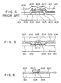
- a semiconductor substrate and a semiconductor for a light valve are already known in which a single-crystal silicon thin film device forming layer is formed on an insulating support substrate through an adhesive layer and an insulating layer is formed on the single-crystal silicon thin film device forming layer, respectively.
- Tr formed on the single-crystal silicon on the insulating substrate is operated for a long time, that is, when current flows through the Tr for a long time, the temperature of the single-crystal silicon where the current flow arises due to the heat produced.
- the temperature of an electrical insulator or thin single-crystal silicon film rises, the produced heat is hardly released and the temperature continuously rises as long as current flows because semiconductive single-crystal silicon is thin and the thin single-crystal silicon is surrounded by electrical insulators and air.
- MOS Tr which is the most popular in the MIS Tr is described below for easy understanding. Every description of the MOS Tr below is also applied to the MIS Tr.
- Figure 6 shows a sectional view of a MOS Tr formed on a substrate in which a thin single-crystal silicon layer 602 with a thickness of 0.1 to several ⁇ m is formed on a quartz layer 601 with a thickness of several hundreds to 1,000 ⁇ m.
- Symbols 603 and 604 are source and drain of the MOS Tr
- 605 is a well region
- 606 is a gate oxide
- 607 is a gate made of Poly-Si.
- Symbol 608 is a channel serving as a current path of the MOS Tr.
- the upper portions of the source 603, drain 604 and gate 607 are covered with an insulator such as a silicon oxide or silicon nitride film.
- Quartz serving as an electrical insulator is also present under the thin single-crystal silicon layer 602. Therefore, when current flows through the channel 608 serving as a current path and heat is produced, the heat of the channel 608 is hardly released and the temperature around the channel 608 is raised because the upper portion of the channel 608 is surrounded by the electrical insulating film such as the silicon oxide film or silicon nitride film, and the insulator of the quartz 601 under the single-crystal silicon layer 602.
- Figure 7 shows another sectional view of the MOS Tr formed on a single-crystal silicon layer on an electrical insulator.
- Symbol 701 is a silicon oxide with a thickness of over 100 nm to several ⁇ m and 702 is a thin single-crystal silicon layer with a thickness of 1 to several ⁇ m.
- the MOS Tr is formed by forming a well 703, source 704 and drain 705 in the thin single-crystal silicon layer 702 and also forming a gate 707 comprising a gate oxide 706 and Poly-Si.
- Symbol 709 is an inter-layer insulating film made of a silicon oxide and 710 is metal aluminium which is connected to the source 704 and drain 705 separately.
- Symbol 711 is a passivation film made of a silicon nitride film, 712 is an adhesive with a thickness of several ⁇ m, and 713 is a glass substrate with a thickness of over hundred to 1,000 ⁇ m.
- the present invention proposes to provide a semiconductor device which integrated circuit comprises a miniaturised Tr, on a SOI wafer, or a Poly-Si formed on an insulating substrate, or a transistor formed in a-Si with a high reliability by preventing the temperature of the single-crystal silicon from rising.
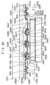
- a semiconductor for a light valve substrate has formed thereon a group of pixel switching transistors (hereafter referred to as Sw-Tr group) for selectively supplying electric power to a pixel electrode and a driving circuit for driving the pixel Sw-Tr group.
- Sw-Tr group a group of pixel switching transistors
- a high voltage of approximately 15 V is applied to the gate electrode and drain electrode of a pixel Sw-Tr to selectively operate the Sw-Tr when the Sw-Tr comprises a MOS Tr.
- Figure 8 shows a sectional view of an N-type MOS Tr formed on a thin single-crystal silicon layer 802 on an electrical insulator 801.
- Symbol 801 is a silicon oxide with a thickness of 0.1 to several ⁇ m
- 802 is a thin single-crystal silicon layer with a thickness of 0.1 to 2 ⁇ m
- 803 is a P-well
- 804 and 805 are source and drain respectively.
- Symbol 806 is a gate insulator made of a silicon oxide and 807 is a gate made of Poly-Si.
- Symbol 808 is a channel serving as a current path of the MOS Tr.
- the source 804 is grounded and a high voltage of 15 V is applied to the drain 805 and the gate 807.
- a high voltage of 15 V is applied to the drain 805 and the gate 807.
- no electric field is generated between the gate and drain at both sides of the gate insulator 806.
- an intense electric field is applied to the gate insulator close to the source.
- a new problem is caused by two events high temperature and intense electric field. That is, a lot of trap levels for capturing carriers flowing through the channel 808 are generated in the vicinity of the source 804. Because a lot of flowing carriers are captured by these traps, a problem occurs that the threshold voltage (gate voltage when current starts flowing between source and drain; hereafter referred to as Vt) of the N-type MOS Tr slowly rises while current flows.
- Vt threshold voltage when current starts flowing between source and drain
- Vt of the P-type MOS Tr fluctuates in the direction in which the absolute value of Vt increases. This is because, when flowing carriers are captured by traps of a gate insulator, a gate voltage with a high absolute value is required to form a channel, that is, to invert a well layer just under the gate insulator 806.
- the voltage to be applied to the Sw-Tr group of a pixel section requires a high voltage of 10 V or higher, for example, 15 V in order to drive a liquid crystal.
- the voltage to be applied to most transistors of a driving circuit section is a relatively low voltage of 5 V or lower.
- the intensity of the electric field applied between the gate and source of most transistors constituting the driving circuit is approximately 1/3 as low as that of the electric field applied between the gate and source of the Sw-Tr of the pixel section.
- the number of trap levels of carriers generated in a gate insulator relates to a high temperature of the channel section and the intensity of an electric field between a gate and source. A lot of trap levels are not generated by only one of the two factors, for example, only the high temperature of the channel section.
- the density of traps generated in the gate insulator increases as the temperature of the channel section gets higher and the intensity of the electric field between the gate and source gets higher.
- a semiconductor device for a light valve arrangement has formed on single crystal silicon on an electrical insulator, a pixel Sw-Tr group for selectively supplying electric power to pixel electrodes and a driving circuit for driving the pixel Sw-Tr group.
- Some of the transistors constituting the driving circuit and all of the Sw-Tr's of the pixel section are main transistors having Vt fluctuations when a high-intensity electric field is applied between a gate and drain. A large current flows through the channel, the channel temperature rises, a high-intensity electric field is applied between a gate and source, and carrier trap levels are generated in a gate oxide.
- Vt fluctuations of a transistor in which a high voltage is applied to the gate and drain of the semiconductor device It is desirable to minimise the Vt fluctuations of a transistor in which a high voltage is applied to the gate and drain of the semiconductor device.
- a semiconductor substrate for a light valve having a structure according to the prior art shown in figure 9 also has a problem in that the Vt of a MOS transistor increases due to the operation of the MOS transistor, when the MOS transistor is formed on a single-crystal silicon thin-film device forming layer.
- symbol 901 is a single-crystal silicon thin-film device forming layer
- 902 is an insulating layer
- 903 is an adhesive layer
- 904 is an insulating support substrate.
- one surface of the single-crystal silicon thin-film device forming layer 901 contacts the thick insulating support substrate 904 with a low heat conductivity through the adhesive layer 903 and the other surface of the layer 901 contacts the air with a low heat conductivity through the insulating layer 902.
- the heat produced due to the operation of a MOS transistor is stored in the single-crystal silicon thin-film device forming layer and a lot of carriers are deeply trapped in the gate insulator of the MOS transistor, and accordingly the Vt of the MOS transistor is increased.
- a semiconductor device comprising:
- a light valve device comprising a semiconductor device according to the first aspect of the present invention wherein said integrated circuit comprises:
- Fig. 10 shows a sectional view of a normal MOS Tr on an electrical insulator.
- Symbol 1001 is an electrical insulator such as a silicon oxide or quartz
- 1002 is a thin single-crystal silicon film with a thickness of 0.1 to 2 ⁇ m
- 1003 is a P-well containing P-type impurities at a low concentration
- 1004 and 1005 are a source and drain containing N-type impurities at a high concentration having the conducting type opposite to that of the P-well
- 1007 is a gate made of a Poly-Si film.
- Vt of the Tr changes according to elapse of time as shown in Fig. 11.
- Fig. 12 shows a sectional view of a MOS Tr having the LDD structure on an electrical insulator.
- the name of each portion corresponding to that of the portion in Fig. 10 is omitted for simplification.
- Symbols 1201 and 1202 are source and drain containing N-type impurities at a high concentration of approx. 1 x 10 20 cm -3 respectively and 1203 and 1204 are a source and drain containing N-type impurities at a relatively low concentration of approx. 1 to 5 x 10 18 cm -3 respectively.
- Symbol 1205 is a side spacer made of a silicon oxide film formed to make the LDD structure.
- the source 1203 and drain 1204 at a relatively low impurity concentration are formed through ion implantation before the side spacer 1205 is formed and the source 1201 and drain 1202 at a high impurity concentration are formed through ion implantation after the side spacer 1205 is formed.
- Symbol 1206 is a gate.
- Figs. 10 and 12 show the length of the gates 1007 and 1006 as L.
- the current flowing through the MOST Tr having the LDD structure in Fig. 12 is less than the current flowing through the normal MOS Tr in Fig. 10 even if the gate length is the same because the source 1203 and drain 1204 at a relatively low impurity concentration having the LDD structure serve as resistances when the same voltage is applied between the source and drain at a high impurity concentration.
- Fig. 11 shows the value of the Vt fluctuation at the time t1 when variously changing the gate length L in the normal-structure MOS Tr shown in Fig. 10 and the LDD-structure MOS Tr shown in Fig. 12.
- Symbol 1301 is the value of ⁇ Vt of the LDD-structure MOS Tr and 1302 is the value of ⁇ Vt of the normal-structure MOS Tr.
- Fig. 14 shows a perspective view showing the constitution of a semiconductor device for a light valve serving as an active-matrix arrangement.
- Symbol 1401 is a silicon oxide serving as an electrical insulating substrate and 1402 is a thin single-crystal silicon semiconductor film formed on the electrical insulating substrate 1401.
- Symbol 1403 is a driving electrode for driving each pixel and no opaque single-crystal silicon is left under the driving electrode 1403.
- Symbol 1404 is a pixel Sw-Tr for selectively supplying electric power to the driving electrode of each pixel.
- the pixel Sw-Tr comprises a MOS Tr.
- Symbol 1405 is a signal line connected to the drain electrode of each pixel Sw-Tr 1404.
- Symbol 1406 is a scanning line connected to the gate electrode of each pixel Sw-Tr 1404.
- Symbol 1407 is an X driver sending a signal to each signal line 1405 and 1408 is a Y driver for sending a signal to each scanning line 1406.
- the driving electrode 1403 of each pixel, pixel Sw-Tr 1404, signal line 1405, scanning line 1406, X driver 1407, and Y driver 1408 are formed in the single-crystal silicon semiconductor film 1402 or on the single-crystal silicon semiconductor film 1402 through an insulator.
- the X driver 1407 and Y driver 1408 comprise at least a CMOS Tr comprising an N-type MOS Tr and P-type MOS Tr.
- the present invention is characterized by making the gate length of the pixel Sw-Tr serving as a MOS Tr larger than the minimum gate length among the gate lengths of many MOS Tr's forming a driving circuit comprising the X driver 1407 and Y driver 1408 in Fig. 14 for driving a pixel Sw-Tr formed on thin single-crystal silicon on an electrical insulator in order to minimize the Vt fluctuation of the pixel Sw-Tr caused by a high voltage of approx. 15 V applied to the gate and drain electrodes of the pixel Sw-Tr. If the minimum gate length among the gate lengths of many MOS Tr's forming the driving circuit is 2 ⁇ m, the gate length of the pixel Sw-Tr is set to 4 to 5 ⁇ m.
- the Vt fluctuation of the pixel Sw-Tr further decreases even if a high voltage of 15 V is applied to gate and drain.
- the pixel Sw-Tr is described above by taking an N-type MOS Tr as an example. However, a P-type MOS Tr can be also used. The characteristics shown in Figs. 11 and 12 are also directly applicable to a P-type MOS Tr formed on thin single-crystal silicon on an electrical insulator.
- Fig. 15 shows a sectional view of a pixel Sw-Tr.
- Symbol 1501 is a silicon oxide or quartz plate serving as an electrical insulator
- 1502 is single-crystal silicon semiconductor with a thickness of 0.1 to 2 ⁇ m formed like an island on the electrical insulator 1501
- 1503 and 1504 are a source and drain of a P-type MOS Tr respectively
- 1505 is a gate made of a Poly-Si film
- 1506 is a gate oxide made of a silicon oxide.
- Symbol 1507 shown by a broken line is an edge of depletion layer produced when a negative voltage is applied to the drain 1504 and gate 1505. The depletion layer is produced at the top and right side of the broken line 1507.
- Symbol 1508 is an incident light and 1509 and 1510 are an electron and hole produced in the depletion layer due to the incident light 1508.
- the hole 1510 produced due to light reaches a drain electrode by an electric field in the depletion layer and serves as drain current.
- the electron reaches a substrate electrode if it is present nearby. However, if there is no substrate electrode nearby, the electron accumulates in the vicinity of the edge of depletion layer 1507, lowers a potential barrier between source and substrate, and pull the hole out of a source electrode.
- an electron-hole pair produced due to light in the depletion layer increases leak current and degrades transistor characteristics, particularly decreases the ON/OFF ratio.
- Fig. 14 shows a constitution of a semiconductor device for a light valve serving as an active-matrix arrangement.
- An active-matrix light valve substrate arrangement though it is omitted in Fig. 14 makes an image by forming a liquid crystal layer at the bottom of the arrangement through the silicon oxide 1401 of a pixel section comprising the pixel Sw-Tr group 1404 and pixel driving electrode group 1403, applying light vertically to the surfaces of the silicon oxide 1401 and single-crystal silicon semiconductor film 1402 from the liquid crystal layer side or pixel section side where the pixel Sw-Tr group and pixel driving electrode group are formed, and passing or interrupting the light while turning on/off each pixel Sw-Tr.
- a shading film for interrupting light is formed at the top or bottom of each pixel Sw-Tr so as to prevent the light from striking against the pixel Sw-Tr as much as possible. In fact, however, light incoming from a portion with no shading film strikes against the pixel Sw-Tr.
- Fig. 16 shows a top view of the picture element Sw-Tr in Fig. 15.
- Symbol 1611 is a gate made of polycrystal silicon
- 1612 and 1613 are a source and drain containing P-type impurities at a high concentration respectively
- 1614 is a single-crystal silicon island
- 1615 is an electrical insulator such as silicon oxide or quartz plate under a thin single-crystal silicon layer.
- L is the length of the gate 1611 and W is the width of the gate.
- the gate width of the pixel Sw-Tr is minimized to decrease the area of single-crystal silicon under a gate. That is, the gate width of the pixel Sw-Tr is made equal to or smaller than the minimum gate width among the gate widths of many MOST-Tr's in a driving circuit.
- the Tr size decreases by decreasing the gate width, the heat producing region decreases and the amount of heat to be produced also decreases even if a high voltage is applied and a large current flows.
- Fig. 17 (A) shows a top view of the pixel Sw-Tr of the semiconductor device for a light valve substrate of the present invention
- Fig. 17 (B) shows a top view of the MOS Tr of the driving circuit of the present invention.
- symbols 1701 and 1707 are gates made of Poly-Si
- 1702 and 1708 are sources containing P-type impurities at a high concentration
- 1703 and 1709 are drains containing P-type impurities at a high concentration
- 1704 and 1705 are a source and drain containing P-type impurities at a relatively low concentration respectively
- 1706 and 1710 are electrical insulators made of a silicon oxide film or quartz plate under single-crystal silicon.
- the pixel Sw-Tr in Fig. 17 (A) is a P-type MOS Tr having the LDD structure and the MOS Tr in Fig. 17 (B) is a Tr having the minimum gate length and width among the gate lengths and widths of many MOST Tr's in a driving circuit.
- the Vt hardly changes with time and the leak current caused by light can be minimized by setting the gate length and width to the above values and applying the LDD structure to the pixel Sw-Tr.
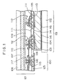
- Fig. 1 shows an example of a light valve device using a semiconductor device which does not form a part of the claimed invention as a driving substrate, particularly shows an active-matrix liquid-crystal light valve device.
- the light valve device has a structure in which a driving substrate 101 comprising the semiconductor device of the present invention and a facing substrate 102 made of transparent glass are bonded each other through a spacer 103 and liquid crystal 104 serving as an electrooptical material is sealed between the both substrates.
- the driving substrate 101 has a structure in which an integrated circuit formed on a single-crystal silicon layer 106 formed on an electrical insulator 105 is copied to a holding member 108 by an adhesive layer 107.
- a silicon oxynitride film or silicon nitride film 110 is formed on the top layer of a passivation film 109 for protecting the integrated circuit.
- the passivation film 109 effectively protects the integrated circuit from moisture and hydrogen contained in the adhesive layer 107. Therefore, electrical characteristics can be prevented from degrading.
- the driving substrate 101 is divided into a peripheral driver circuit section 150 and a pixel section 151.
- a pixel electrode 111 arranged like a matrix and a pixel Sw-Tr 112 for driving the electrode 111 are integrally formed on the pixel section.
- the peripheral driver circuit section is covered with a shading film 113 from the back.
- the pixel Sw-Tr is also covered with the shading film 113 from the back.
- An liquid crystal allignment layer 114 is formed at the back of the picture element section of the driving substrate 101.
- a common electrode 115 and liquid crystal allignment layer 116 are formed on the inner surface of the facing substrate 102.
- the pixel Sw-Tr 112 uses a P-type MOS Tr having the LDD structure as shown in Fig. 1, it can also use an N-type MOS Tr having the LDD structure.
- an N-type MOS Tr 117 is drawn at the driving circuit section.
- the driving circuit section includes a lot of N- and P-type MOS Tr's
- the N-type MOS Tr 117 shown in Fig. 1 is a Tr having the minimum gate length among those MOS Tr's.
- the gate length of the N-type MOS Tr's in the driving circuit section is L2 and that of the P-type MOS Tr's in the driving circuit section is L1.
- L1 is larger than L2.
- the gate width W1 of the picture element Sw-Tr 112 is made smaller than the minimum gate width W2 among the gate widths of many MOS Tr's in the driving circuit section.
- the leak current of the pixel Sw-Tr caused by light becomes very small.
- Fig. 18 shows an example which does not form a part of the claimed invention.
- Symbol 1801 is a single-crystal silicon substrate
- 1802 is a silicon oxide embedded in the single-crystal silicon substrate 1801 and serving as an electrical insulator
- 1803 is a thin single-crystal silicon layer on the silicon oxide 1802.
- the silicon oxide 1802 has a thickness of over hundred ⁇ ngstroms to several microns and the thin single-crystal silicon layer 1803 also has a thickness of over hundred ⁇ ngstroms to several microns.
- Fig. 19 shows another example which does not form a part of the claimed invention.
- Symbol 1901 is a single-crystal silicon substrate
- 1902 is an electrical insulator with a thickness of over hundred ⁇ ngstroms to several microns embedded in the single-crystal silicon substrate 1901
- 1903 is a thin single-crystal silicon layer with a thickness of over hundred ⁇ ngstroms to several microns on the silicon oxide 1902.
- Symbol 1904 is a circuit 1 formed in a region at the left of the single-crystal silicon substrate 1901 and where no electrical insulator is embedded
- 1906 is a circuit 3 in a region at the right of the single-crystal silicon substrate and where no electrical insulator is embedded
- 1905 is a circuit 2 formed on a thin single-crystal silicon layer above the electrical insulator 1902.
- the circuits 1904, 1905, and 1906 are electrically connected to each other to form an integrated circuit having a function.
- the circuit 1 of 1904 and the circuit 3 of 1906 have a high operation frequency and therefore, they have a large power consumption. However, there is no electrical insulator under the circuit 1 of 1904 or circuit 3 of 1906.
- the circuit 2 of 1905 formed on a thin single-crystal silicon layer 1903 has a low operation frequency and a small power consumption, and hardly produces heat. Therefore, no heat is accumulated in the single-crystal silicon layer 1903 even if the electrical insulating film 1902 is present under the thin single-crystal silicon layer 1903.
- a high operation speed is required for the circuit 2 of 1905, it can be easily obtained because the circuit 2 of 1905 is formed on an SOI from which the high operation speed of the circuit can be obtained.
- Fig. 20 shows still another example which does not form a part of the claimed invention.
- the example shown in Fig. 20 is almost common to the example shown in Fig. 19. Therefore, descriptions of the names of the portions 1901 to 1906 common to those in Fig. 19 are omitted.
- Fig. 20 part of single-crystal silicon is removed from the silicon oxide 1902 serving as an electrical insulator embedded in part of the region of the single-crystal silicon substrate 1901.
- Symbols 2001 and 2002 are silicon nitride films which serve as masks for removing the single-crystal silicon under the silicon oxide 1902.
- KOH solution potassium hydroxide solution
- the silicon oxide 1902 serves as a stopper when etching single-crystal silicon with the KOH solution and also prevents the thin single-crystal silicon film 1903 on the silicon oxide 1902 from being etched.
- Symbols 2003 and 2004 are portions where some of the single-crystal silicon 1901 is left under the silicon oxide 1902.
- Fig. 21 shows still another example which does not form a part of the claimed invention.
- the example shown in Fig. 21 is almost common to the examples shown in Figs. 19 and 20. Therefore, descriptions of the names of the portions 1901 and 1906 and 2001 and 2002 common to those in Figs. 19 and 20 are omitted.
- Fig. 21 is different from the example in Fig. 20 only in the fact that symbols 2003 and 2004 which are a part of the single-crystal silicon 1901 respectively are absent under the silicon oxide 1902 shown in Fig. 20. That is, Fig. 21 shows a structure in which the single-crystal silicon 1901 under the silicon oxide 1902 is entirely removed.
- the example in Fig. 21 has a structure in which any other arrangement can be easily set to the portion from which the single-crystal silicon 1901 under the silicon oxide 1902 is removed because the portion is larger than that of the example in Fig. 20.
- Fig. 22 shows a sectional view of an active matrix light-valve device serving as an example of a semiconductor device which does not form a part of the claimed invention.
- This semiconductor device has a structure in which a transparent substrate 2223 is bonded to the semiconductor device shown in Fig. 20 by adhesive and a facing substrate 2226 is set under a silicon oxide 2202 so that the liquid crystal layer 2224 is put between the substrate 2226 and the silicon oxide 2202. The following is the description of each portion in Fig. 22.
- Symbol 2201 is a single-crystal silicon substrate containing P-type impurities at a low concentration (e.g. approx. 1 x 10 16 cm -3 ), which is present at the right and left of Fig 22.
- a silicon oxide 2202 with a thickness of over hundred ⁇ ngstroms to several microns serving as an electrical insulator film is present at the center of Fig. 22 and three islands of single-crystal silicon 2203 containing N-type impurities at a low concentration (e.g. approx. 1 x 10 16 cm -3 ) are arranged in the lateral direction.
- Fig. 22 it is shown that three islands of a single-crystal silicon layer are arranged and a MOS Tr is formed on each island. However in fact, over ten to thousands of islands are arranged.
- Symbol 2204 is a field oxide made of a silicon oxide with a thickness of over thousand ⁇ ngstroms for isolating device formed on the single-crystal silicon substrate 2201.
- a MOS Tr is formed on each of three islands of a thin single-crystal silicon layer on the silicon oxide 2203.
- Each MOS Tr serves as a switching transistor in each pixel section of an active-matrix arrangement.
- Each of three switching transistors comprises a thin single-crystal silicon 2203 with a thickness of over hundred ⁇ ngstroms to several microns containing N-type impurities at a low concentration, a drain 2205 and source 2206 containing P-type impurities at a high concentration (e.g. approx. 1 x 10 20 cm -3 ), a gate insulator 2207, and a gate 2208.
- Symbol 2209 is an insulating film for preventing electrical continuity between a transparent pixel electrode 2229 made of a thin Poly-Si film with a thickness of over hundred to 2,000 ⁇ ngstroms and a thin single-crystal silicon layer 2203.
- the insulating film 2209 is a silicon oxide with a thickness of over hundred to 1,000 ⁇ ngstroms deposited through the chemical vapor deposition.
- Symbol 2210 is an intermediate insulating film made of a silicon oxide for preventing electrical continuity between a drain wire 2211 made of a metal such as aluminum or the like and gate electrode 2208, and between a drain 2211 and transparent pixel electrode 2229.
- the N-type MOS Tr is present on the single-crystal silicon substrate 2201 at the left of Fig. 22.
- the N-type MOS Tr comprises a source 2213 and drain 2214 containing N-type impurities at a high concentration (approx. 1 x 10 20 cm -3 ), a gate insulator 2215, gate electrode 2216, and single-crystal silicon substrate 2201 containing P-type impurities.
- the drain wire 2211 made of a metal such as aluminum or the like connected with the drain 2214 of the N-type MOS Tr connects with each drain 2205 of three pixel Sw-Tr's made of a P-type MOS Tr on the silicon oxide 2202 and supplies a voltage to give electric charges to the transparent pixel electrode 2229. That is, the N-type MOS Tr serves as a part of a driving circuit for driving the pixel Sw-Tr and the driving circuit is formed on the single-crystal silicon substrate 2201.
- an N-type MOS Tr is present on a single-crystal silicon substrate at the right of Fig. 22.
- the N-type MOS Tr comprises a source 2217 and drain 2218 containing N-type impurities at a high concentration (e.g. approx. 1 x 10 20 cm -3 ), a gate insulator 2219, a gate electrode 2220, and a single-crystal silicon substrate 2201 containing P-type impurities.
- the source 2217 and drain 2218 of the N-type MOS Tr connect with a metallic wire 2212 made of aluminum or the like.
- Each N-type MOS Tr on a single-crystal silicon substrate at the right and left of Fig. 22 and three P-type MOS Tr's serving as pixel Sw-Tr's on the silicon oxide 2202 at the center of Fig. 22 are finally electrically connected each other at a not-illustrated portion to constitute an integrated circuit having a certain function.
- Symbol 2221 is a passivation film made of a silicon nitride film for covering the entire integrated circuit.
- Symbol 2223 is a transparent substrate made of quartz with a thickness of over hundred to 1,000 microns, which is bonded to the single-crystal silicon substrate 2201 by an adhesive 2222.
- the liquid crystal layer 2224 is sealed in a region enclosed by a sealing material 2225 and facing transparent substrate 2226 under the silicon oxide 2202.
- a liquid crystal allignment layer 2227 for orienting liquid crystal is formed at a portion contacting the liquid crystal layer at the bottom of the silicon oxide 2202 on the facing transparent substrate 2226.
- a common electrode 2228 made of ITO or the like is formed on the facing transparent substrate 2226.
- the optically-opaque drain wire 2211 made of aluminum is arranged on three pixel Sw-Tr's.
- the width of the aluminum wire is as small as several microns, the drain wire 2211 made of aluminum cannot be seen when drawing a sectional view slightly back or slightly this side of the sectional view in Fig. 22.
- the top and bottom of the transparent picture element electrode 2229 become entirely transparent. Therefore, whenever each pixel Sw-Tr is turned on/off, a voltage is applied or not applied between each transparent picture element electrode 2229 and common electrode 2228, that is, to the liquid crystal layer under each pixel electrode.
- the light of a lamp set under the facing transparent electrode 2226 passes through a portion where each pixel Sw-Tr is turned on but the light is interrupted at a portion where it is turned off and a picture is displayed.
- a pixel Sw-Tr group is formed on the optically-transparent silicon oxide film 2202, the optically-opaque single-crystal silicon under the silicon oxide film 2202 is removed, and a liquid crystal is set to the portion where the silicon oxide 2202 is removed.
- the semiconductor device can be used as a light valve substrate device.
- the driving circuit section with a high operation frequency for driving the pixel Sw-Tr group is formed on the single-crystal silicon substrate 2201, the heat produced due to the operation of the driving circuit is easily released to the single-crystal silicon substrate 2201. Therefore, carrier trap levels do not increase due to temperature rise in many MOS Tr's constituting the driving circuit. Thus, there is an excellent advantage that the driving circuit operates stably.
- Fig. 23 is a sectional view showing a method for fabricating the semiconductor device of the present invention.
- Symbol 2301 is a single-crystal silicon substrate and 2302 is resist with a thickness of several microns.
- a window is opened on the resist 2302 at the center of the single-crystal silicon substrate 2301 to implant oxygen ions 2303.
- Oxygen ions are implanted at a proper acceleration energy so that a single-crystal silicon layer with a desired depth is left on the single-crystal silicon surface.
- implanted oxygen ions react on the sill by heating the single-crystal silicon substrate 2301 at a temperature of 1,000 °C or higher and a silicon oxide is formed, and thereby the semiconductor device of the present invention is formed.
- Fig. 24 shows a sectional view of the semiconductor device of the present invention.
- Symbol 2401 is a thin single-crystal silicon layer
- 2402 is a silicon oxide
- 2403 is an aluminum nitride layer
- 2404 is a single-crystal silicon substrate with a thickness of over hundred to 1,000 ⁇ m.
- the thin single-crystal silicon layer 2401, silicon oxide 2402, and aluminum nitride layer 2403 have a thickness of over hundred ⁇ ngstrom.
- the heat produced in the thin single-crystal silicon layer 2401 passes through the silicon oxide 2402 because the aluminum nitride layer 2403 with a high heat conductivity, and then it is transmitted to the aluminum nitride layer 2403, and finally released to the thick single-crystal silicon substrate 2404 serving as a heat sink.
- the heat conductivities of a silicon oxide, aluminum nitride and single-crystal silicon are 0.014 W/cm ⁇ °K, 2.5 W/cm ⁇ °K, and 1.5 W/cm ⁇ °K respectively. Therefore, the heat conductivity of aluminum nitride is approx. 180 times as large as that of the silicon oxide film, and is larger than that of single-crystal silicon. Thus, it is found that aluminum nitride has an excellent heat conductive characteristic.
- the silicon oxide 2402 is present just under the thin single-crystal silicon layer 2401 on which an integrated circuit is formed. This is not only because a silicon oxide is stable as an insulator and has a high reliability but because the silicon oxide is the best insulating film as an insulating film not affecting the single-crystal silicon layer when considering an insulating film contacting single-crystal silicon.
- Fig. 25 shows a sectional view of the semiconductor device of another embodiment of the present invention obtained at present.
- the number and name of each portion in Fig. 25 are the same as those of each portion in Fig. 24. Therefore, descriptions of them are omitted for simplification.
- the name of the portion corresponding to the number is the same as the name already described. Therefore, the description of it is hereafter omitted.
- Fig. 25 is different from Fig. 24 only in the fact that the thickness of the aluminum nitride layer 2403 is larger than that of the silicon oxide 2402,
- the heat produced in the thin single-crystal silicon layer 2401 very easily passes through the thin silicon oxide 2402 and easily reaches the aluminum nitride layer 2403 with a high heat conductivity when the integrated circuit formed on the thin single-crystal silicon layer 2401 operates as described above.
- the heat described above easily reaches the thick silicon substrate 2404 serving as a heat sink to prevent the temperature of the thin single-crystal silicon layer 2401 from rising.
- Fig. 26 is a sectional view of still another embodiment of the semiconductor device of the present invention.
- the aluminum nitride layer 2403 is present as an insulating film under the thin single-crystal silicon layer 2401 serving as an SOI.
- the heat produced due to the operation of the integrated circuit formed on the thin single-crystal silicon layer 2401 is directly transmitted to the aluminum nitride layer 2403 with a high heat conductivity and easily released to the single-crystal silicon substrate serving as a heat sink.
- Fig. 27 is a sectional view of still another embodiment of the semiconductor device of the present invention.
- Symbol 2701 is a thin single-crystal silicon layer
- 2702 and 2704 are aluminum nitride layers
- 2703 is a silicon oxide
- 2705 is a thick single-crystal silicon substrate.
- an insulating film under the thin single-crystal silicon layer 2701 serving as an SOI layer has a three-layer structure in which the silicon oxide 2703 is formed between the aluminum nitride layers 2702 and 2704.
- the aluminum nitride layer with a high heat conductivity contacts both the thin single-silicon layer 2701 and thick single-crystal silicon substrate 2705 and the heat produced due to the operation of the integrated circuit formed the thin single-crystal silicon layer is easily released to the thick single-crystal silicon substrate 2705 serving as a heat sink.
- Figs. 28 (a) to 28(c) are sectional views of the steps showing a fabrication method of the semiconductor device of the present invention.
- the fabrication method in Figs. 28 (a) to 28 (c) uses an SOI wafer forming method according to the bonding method.
- symbol 2801 is a single-crystal silicon substrate and 2802 is a silicon oxide obtained by oxidizing the single-crystal silicon substrate 2801.
- the silicon oxide 2802 has a thickness of over hundred ⁇ ngstroms to several ⁇ m.
- the single-crystal silicon substrate 2801 on which the silicon oxide 2802 is formed is assumed as substrate A.
- Symbol 2804 is another single-crystal silicon substrate and 2803 is an aluminum nitride layer formed on the surface of the single-crystal silicon substrate 2804.
- the single-crystal silicon substrate 2804 on which the aluminum nitride layer 2803 is formed is assumed as substrate B.
- the substrate A is bonded with the substrate B in a high-temperature vacuum or a high-temperature oxygen atmosphere of 900 to 1,200 °C so that the silicon oxide 2802 faces the aluminum nitride layer 2803.
- the single-crystal silicon substrate 2801 on which the silicon oxide 2802 is formed is removed up to a desired thickness through grinding and/or etching.
- the thin single-crystal silicon layer 2805 serving as an SOI layer is formed on the aluminum nitride layer 2803 and silicon oxide 2802.
- the silicon oxide 2802 formed by oxidizing the single-crystal silicon substrate 2801 is present just under the thin single-crystal silicon layer 2805 serving as an SOI layer on which an integrated circuit is formed and the boundary between the single-crystal silicon layer 2805 and silicon oxide 2802 is kept in a preferable state.
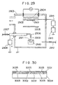
- Fig. 29 is a schematic view of an arrangement for forming an aluminum nitride layer.
- a method for forming an aluminum nitride layer above a single-crystal silicon substrate through the ion plating method is described below by referring to Fig. 29.
- a single-crystal silicon substrate 2901 is set to a substrate holder 2902.
- a vacuum vessel 2903 is brought into a high vacuum state of, for example, 0.01 m Torr or lower.
- the temperature of the vacuum vessel 2903 is raised to, for example, 300 to 400 °C by a heater 2904 to exhaust unnecessary gas out of the single-crystal silicon substrate 2901, substrate holder 2902, and vacuum vessel 2903 (degassing).
- the degassing increases the adhesion of aluminum nitride to be adhered to the single-crystal silicon substrate.
- argon gas is supplied to a hollow cathode 2906 through an argon gas introduction tube 2907 while keeping a shutter 2905 close.
- a hollow-cathode power supply 2908 is turned on to start hollow-cathode discharge.
- aluminum 2911 in a crucible 2910 is heated.
- the heated aluminum evaporates.
- the discharge current by the hollow cathode is, for example, 200 A and the argon gas flow rate is 18 SCCM (18 CC per min).
- Nitrogen gas N2 is introduced through a gas introduction port 2912 to adjust the nitrogen partial pressure.
- the nitrogen partial pressure is, for example, 2 m Torr.
- the shutter 2905 is opened to form an aluminum nitride layer on the single-crystal silicon substrate 2901. While the aluminum nitride layer is formed, a high-frequency bias is applied to the single-crystal silicon substrate 2901 from a high-frequency power supply 2913 and an impedance matching box 2914.
- the high-frequency bias removes charges from the substrate and therefore, an aluminum nitride film which is a compound film superior in adhesiveness and crytalinity can be formed on the single-crystal silicon substrate.
- the high-frequency output is, for example, 20 W.
- the aluminum nitride manufacturing method of the present invention described above is called the ion plating method and also called the actuation reaction evaporation method (ARE method).
- ARE method actuation reaction evaporation method
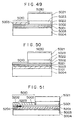
- Fig. 30 shows a sectional view of still another embodiment of the present invention.
- Symbol 3001 is a thin silicon oxide film serving as an SOI layer
- 3002 is a silicon oxide
- 3003 is an aluminum nitride layer
- 3004 is a thick single-crystal silicon film.
- the silicon oxide 3002 is removed from a portion 3005 in a silicon wafer and the aluminum nitride layer contacts the thin single-crystal silicon layer 3001 at the portion 3005.
- the heat produced in the thin single-crystal silicon due to the operation of an integrated circuit formed on the thin single-crystal silicon layer 3001 is transmitted to the aluminum nitride layer 3003 with a high heat conductivity from the portion 3005 where the aluminum nitride layer 3003 directly contacts the thin single-crystal silicon 3001 and released to the single-crystal silicon substrate 3004 serving as a heat sink. Therefore, for the semiconductor device of the present invention shown in Fig. 30, the temperature of the thin single-crystal silicon layer 3001 is prevented from rising even while the integrated circuit operates.
- a method for fabricating the semiconductor device of the present invention is described below by referring to the sectional views of steps in Figs. 31 (a) to 31 (d) and Figs. 32 (a) to 32 (d).
- symbol 3101 is a single-crystal silicon substrate
- 3102 is a silicon oxide obtained by oxidizing the single-crystal silicon substrate
- 3103 is a resist film applied onto the silicon oxide.
- a resist window 3104 is formed on a portion of the resist film 3103 through the step of photolithography. Thereafter, the silicon oxide in which the surface of the portion with the resist window 3104 formed is exposed is etched through ion etching.
- a portion of the silicon oxide is etched and the surface of the single-crystal silicon substrate is exposed at the portion.
- the aluminum nitride layer 3105 is formed on the single-crystal silicon substrate in which the silicon oxide is left at a portion of the surface. Moreover, the silicon oxide 3106 formed through chemical vapor deposition is deposited on the layer 3105. In this case, the surface of the aluminum nitride layer 3105 is not flat but the surface of the thickly-deposited silicon oxide 3106 is flat.
- Fig. 32 (a) when the whole of the silicon oxide 3106 formed through chemical vapor deposition and a portion of the aluminum nitride layer 3105 are removed by grinding or polishing, the aluminum nitride layer 3105 with a very flat surface is formed.
- the single-crystal silicon substrate 3101 on which the silicon oxide 3102 and very-flat aluminum nitride layer 3105 are formed is assumed as substrate C.
- Fig. 32 (b) the substrate C and a new single-crystal silicon substrate 3106 are prepared (this is assumed as substrate D).
- the substrates C and D are bonded each other in a high-temperature vacuum or high-temperature oxygen atmosphere of 900 to 1,200 °C so that the aluminum nitride layer 3105 is present between the substrates.
- the semiconductor device of the present invention having the structure shown in Fig. 30 is obtained by removing the a single-crystal silicon layer of the single-crystal silicon substrate 3101 (substrate C) with the silicon oxide 3102 and aluminum nitride layer 3105 formed up to a desired thickness through grinding and/or etching.
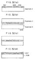
- Fig. 33 is a sectional view of the semiconductor device of still another embodiment of the present invention, which shows a partial sectional view of the semiconductor device in which an integrated circuit is formed on an SOI wafer having a single-crystal silicon layer on an insulator.
- Symbol 3301 is a single-crystal silicon substrate with a thickness of over hundred to 1,000 ⁇ m
- 3302 is an aluminum nitride layer with a thickness of over thousand ⁇ ngstroms to several ⁇ m
- 3303 is a silicon oxide film with a thickness of over thousand ⁇ ngstroms to several ⁇ m.
- Symbol 3304 is a silicon oxide with a thickness of over thousand ⁇ ngstroms for device isolation formed by oxidizing a thin single-crystal silicon layer on the silicon oxide 3303.
- the bottom of the silicon oxide 3304 contacts the silicon oxide 3303.
- Symbol 3305 is a P-well region containing P-type impurities at a concentration of approx. 1 x 10 16 cm -3 in the thin single-crystal silicon layer
- 3306 and 3307 are a source region and drain region containing N-type impurities at a concentration of approx. 1 x 10 20 cm -3 in the thin single-crystal silicon layer respectively.
- Symbol 3308 is a gate insulator made of a silicon oxide film with a thickness of over hundred ⁇ ngstroms formed by oxidizing a thin single-crystal silicon layer and 3309 is a gate made of a polycrystal silicon containing N-type impurities at a high concentration.
- An N-type MOS transistor comprises the gate 3309, gate insulatior 3308, source 3306, drain 3307, and P-well 3305.
- Symbol 3310 is an intermediate insulating film formed by depositing a silicon oxide with a thickness of over thousand ⁇ ngstroms.
- Symbol 3311 is an aluminum layer electrically connecting with the source 3306 and 3312 is an aluminum layer electrically connecting with the drain 3307. The aluminum layers 3311 and 3312 also serve as wiring as they extend to the left and right of Fig. 33.
- Symbol 3313 is a passivation film made of a silicon nitride.
- the aluminum nitride layer 3302 and silicon oxide film 3303 serve as insulators of a single-crystal silicon wafer on insulator (SOI wafer) and an SOI layer comprises the P-well 3305, source 3303, and drain 3307.
- the heat produced in a thin single-crystal silicon layer that is, the P-well 3305, source 3306, and drain 3307 in Fig. 11 is transmitted to the aluminum wiring 3312 and released to the aluminum nitride layer 3302 and the single-crystal silicon substrate 3301 serving as a heat sink through the portion 3314 where the aluminum nitride layer 3302 contacts the aluminum wiring 3312. Therefore, for the semiconductor device having the structure of the present invention shown in Fig. 33, the heat produced in the thin single-crystal silicon layer is not stored in the thin single-crystal silicon layer but it prevents the temperature of the thin single-crystal silicon layer from rising.
- the aluminum nitride layer is described above by taking a material expressed by the chemical formula of AlN as an example.
- a material expressed by the chemical formula of Al x Ny has the almost same heat conductivity as the material AlN.
- the material expressed by the formula of Al x Ny also has the features of the present invention described up to here. Therefore, matters described on the aluminum nitride in the present invention are applied not only to AlN but to Al x Ny.
- a high heat radiation effect is also obtained by using a film made of carbon or sapphire (Al 2 O 3 ) instead of AlN.
- the substrates 2404 and 2804 shown in Figs. 24, 26, and 28 are included in the embodiments of the present invention even if they are transparent substrates made of quartz or glass.
- the silicon oxide, aluminum nitride layer, and quartz can be used for an active-matrix light valve device because they are transparent.
- Fig. 34 shows an embodiment of a light valve device constituted by using the semiconductor substrate of the present invention, in which liquid crystal is used as an electrooptical material.
- the embodiment comprises a semiconductor substrate 3400, a facing substrate 3420 and a liquid crystal layer 3410 filled in the substrate.
- the semiconductor substrate comprises a support substrate 3401 made of a transparent material, an aluminum nitride layer 3402 formed on the support substrate, and a silicon oxide 3419.
- Fig. 34 top and bottom polarizing plates 3417 and 3411 are formed. However, it is not always necessary to bond the polarizing plates to transparent substrates 3416 and 3401 but it is possible to arrange them separately.
- the X and Y drivers constituting the peripheral circuit section comprises the semiconductor device shown in Fig. 33.
- Fig. 34 a structure is shown in which the aluminum nitride layer 3402 is formed on the transparent substrate 3401, for easy understanding. However, it is also possible to form only a necessary portion of the aluminum nitride layer, for example, only the bottom of the peripheral circuit section.
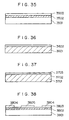
- Fig. 35 shows a sectional view of a semiconductor device which does not form a part of the claimed invention.
- Symbol 3501 is a transparent insulating substrate made of quartz or glass
- 3502 is an insulating film with a high heat conductivity made of aluminum nitride or the like
- 3503 is a semiconductor film made of single-crystal silicon, polycrystal silicon, or a-Si.
- the heat produced in the semiconductor film 3503 is transmitted to the insulating film 3502 made of aluminum nitride or the like with a high heat conductivity without remaining in the semiconductor film 350.
- the insulating substrate 3501 is transparent and the film 3502 is transparent when aluminum nitride is a thin film. Therefore, the example can be applied to a light-transmission-type active-matrix display device.
- Fig. 36 shows a sectional view of still another example of a semiconductor device which does not form a part of the claimed invention.
- Symbol 3601 is an insulating substrate with a high heat conductivity made of aluminum nitride or the like.
- Symbol 3602 is a semiconductor film made of single-crystal silicon, polycrystal silicon, or a-Si.
- the semiconductor device having the structure shown in Fig. 36, when a transistor or integrated circuit formed in the semiconductor film 3602 operates, the heat produced in the semiconductor film 3602 is transmitted to the insulating film 3601 with a high heat conductivity made of aluminum nitride or the like and released to the outside of the semiconductor device without remaining in the semiconductor film 3602.
- Fig. 37 is a sectional view of still another example of a semiconductor device which does not form a part of the claimed invention.
- Symbol 3701 is an insulating substrate with a high heat conductivity made of aluminum nitride or the like.
- Symbol 3702 is a thin insulating film made of a silicon oxide film or the like.
- Symbol 3703 is a semiconductor film made of single-crystal silicon, polycrystal silicon, or a-Si.
- the semiconductor device having the structure shown in Fig. 37 when a transistor or integrated circuit formed in the semiconductor film 3703 operates, the heat produced in the semiconductor film 3703 passes through the thin insulating film 3702 and it is easily released to the insulating film 3701 with a high heat conductivity made of aluminum nitride or the like without remaining in the semiconductor film 3703.
- the insulating film 3702 is used for the structure in Fig. 37 that, if the insulating substrate 3701 with a high heat conductivity is made of aluminum nitride, the aluminum nitride has a piezoelectric characteristic. A transistor and integrated circuit are formed in the semiconductor film 3703 and the current and voltage produced due to the operation of them influence the aluminum nitride having the piezoelectric characteristic, and thereby the semiconductor film 3703 and aluminum nitride 3701 may interact. The thin insulating film 3702 would be able to prevent the interaction.
- the insulating film 3702 is used for the structure in Fig. 37 that it is easier to form a semiconductor film on a silicon oxide film than to directly form the semiconductor film on aluminum nitride with a high heat conductivity.
- aluminum nitride is listed as an insulator with a high heat conductivity.
- the heat conductivity of the aluminum nitride is 2.5 W/cm ⁇ °K at the ordinary temperature as previously described, which is much higher than 0.014 W/cm ⁇ °K which is the heat conductivity of a silicon oxide film serving as an insulating film and also higher than 1.5 W/cm ⁇ °K which is the heat conductivity of single-crystal silicon serving as semiconductor. Therefore, it is understood that aluminum nitride has an excellent heat conductivity.
- Fig. 38 is a sectional view of still another embodiment of the semiconductor device of the present invention.
- Symbol 3801 is a transparent insulating substrate
- 3802 is an insulating film with a high heat conductivity made of aluminum nitride or the like
- 3803 is a silicon oxide film
- 3804 at the top both ends of the silicon oxide film 3803 is a single-crystal silicon layer
- 3805 at the top central portion of the silicon oxide film 3803 is Poly-Si.
- the transparent insulating substrate 3801, aluminum nitride 3802, and silicon oxide film 3803 are all transparent.
- the embodiment as an active-matrix display device by forming, for example, a picture element Sw-Tr group on the polycrystal silicon layer 3805 and a driver circuit for operating the picture element Sw-Tr group on the single-crystal silicon layer 3804.
- the thickness of the silicon oxide film 3803 is not very large, for example, over thousand ⁇ ngstroms.
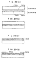
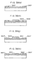
- Figs. 39 (a) to 39 (h) are sectional views of the steps showing the fabrication method of the semiconductor device of the present invention shown in Fig. 38. This method uses the SOI wafer forming method according to the bonding method.
- symbol 3901 is a single-crystal silicon substrate and 3902 is a silicon oxide film obtained by oxidizing the single-crystal silicon substrate 3901.
- the silicon oxide film 3902 has a thickness of over hundred ⁇ ngstroms to several ⁇ m.
- Symbol 3904 is a transparent insulating substrate and 3903 is an aluminum nitride layer formed on the surface of the transparent insulating substrate 3904.
- the substrate A and the substrate B are bonded each other in a high-temperature vacuum or high-temperature oxygen atmosphere of 900 to 1,200 °C so that the silicon oxide film 3902 faces the aluminum nitride layer 3903.
- Fig. 39 (c) the single-crystal silicon substrate 3901 on which the silicon oxide film 3902 is formed is removed up to a desired thickness through grinding and/or etching.
- a thin single-crystal silicon layer 3905 serving as an SOI layer is formed on the aluminum nitride layer 3903 and silicon oxide film 3902.
- resist 3906 is left at the both ends of the thin single-crystal silicon layer 3905 by applying resist onto the single-crystal silicon layer 3905 and removing the central resist through photolithography.
- a single-crystal silicon layer 3907 is left at the top right and left of the silicon oxide film 3902.
- resist 3909 is left at the central portion of Poly-Si 3908 through photolithography by depositing the Poly-Si 3908 and then applying resist to it. Then, in Fig. 40 (g), the Poly-Si 3908 is dry-etched to leave an islanded Poly-Si 3910 under the central resist 3909.
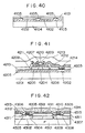
- Fig. 40 shows a sectional view of still another embodiment of the present invention.
- Symbol 4101 is a semiconductor film
- 4102 is a silicon oxide film
- 4103 is an aluminum nitride layer
- 4104 is a thick transparent insulating substrate.
- the silicon oxide film 4102 is removed at a portion 4105 where the aluminum nitride layer contacts the semiconductor film 4101.
- the heat produced in the thin semiconductor film due to the operation of an integrated circuit formed on the semiconductor film 4101 is transmitted to the aluminum nitride layer 4103 with a high heat conductivity through the portion 4105 where the aluminum nitride layer 4103 directly contacts the thin semiconductor film 4101. Therefore, for the semiconductor device of the present invention in Fig. 40, the temperature of the thin semiconductor film 4101 can be prevented from rising even while the integrated circuit operates.
- Fig. 41 is a sectional view of the semiconductor device of still another embodiment of the present invention, which shows a sectional view of a semiconductor film on an insulator, that is, a sectional view of a portion of a semiconductor device in which an integrated circuit is formed on a Poly-Si film.
- Symbol 4201 is an insulating substrate made of glass or quartz
- 4202 is an aluminum nitride layer with a thickness of over thousand ⁇ ngstroms to several ⁇ m
- 4203 is a silicon oxide film with a thickness of over thousand ⁇ ngstroms to several ⁇ m
- Symbol 4204 is a P-well region containing P-type impurities at a concentration of approx. 1 x 10 16 cm -3 in a thin Poly-Si
- 4205 and 4206 are a source region and drain region containing N-type impurities at a concentration of approx. 1 x 10 20 cm -3 in a thin Poly-Si layer respectively.
- Symbol 4207 is a gate insulating film made of a silicon oxide film formed by oxidizing a thin Poly-Si film
- 4208 is a silicon oxide film formed on the side wall of a Poly-Si film when the gate oxide film 4207 is formed
- 4209 is a gate made of Poly-Si containing N-type impurities at a high concentration.
- An N-type MOS transistor comprises the gate 4209, gate insulating film 4207, source 4205, drain 4206, and P-well 4204.
- Symbol 4210 is an intermediate insulating film formed by depositing a silicon oxide film with a thickness of over thousand ⁇ ngstroms.
- Symbol 4211 is an aluminum layer electrically connecting with the source 4205 and 4212 is an aluminum layer electrically connecting with the drain 4206.
- the aluminum layer 4211 also serves as wiring as it extends in the longitudinal direction of Fig. 41 and the aluminum layer 4212 serves as wiring as it extends toward right of Fig. 41.
- Symbol 4213 is a passivation film made of a silicon nitride film.
- the aluminum wiring 4212 contacts the aluminum nitride layer 4202 at a portion 4214.
- the heat produced in a thin Poly-Si film that is, in the P-well 4204, source 4205, and drain 4206 in Fig. 41 is transmitted to the aluminum wiring 4212 and released to the aluminium nitride layer 4202 through the portion 4214 where the aluminium nitride layer 4202 contacts the aluminium wiring 4212. Therefore, for the semiconductor device having the structure of the present invention in Fig. 41, the heat produced in a thin polycrystal silicon film prevents the temperature of the thin polycrystal silicon layer from rising without remaining in the thin polycrystal silicon layer.
- the aluminium wiring 4212 contacts the aluminium nitride layer 4202 at a portion 4214. But it is allowed that the aluminium wiring connecting other terminal like source or well contacts the aluminium nitride layer 4202.
- Embodiments of the present invention for the problem (1) are described below.
- Fig. 44 shows still another embodiment of the present invention
- Figs. 42 and 43 are explanatory diagrams which show examples of semiconductor devices which do not form a part of the claimed invention.
- a portion with the same name is provided with the same number in order to simplify the description.
- symbol 4301 is a single-crystal silicon substrate containing P-type impurities at a low concentration
- 4302 is a P-well containing P-type impurities at a concentration slightly higher than that of the single-crystal silicon substrate
- 4303 and 4304 are a source and drain containing N-type impurities at a high concentration respectively
- 4305 is a gate insulating film
- 4306 is a gate made of Poly-Si containing impurities at a high concentration
- 4307 is an N-well containing N-type impurities at a low concentration
- 4308 and 4309 are a source and drain containing P-type impurities at a high concentration respectively
- 4310 is a gate made of Poly-Si containing impurities at a high concentration.
- Symbol 4311 is a thick silicon oxide film for device isoration
- 4312 is an intermediate film made of a silicon oxide film formed by depositing the silicon oxide film
- 4313 is metal aluminum
- Symbol 4314 is a passivation film with a high heat conductivity.
- the passivation film 4314 has an insulating characteristic and uses, for example, aluminum.
- an N-type MOS Tr comprises the P-well 4302, source 4303, drain 4304, gate insulating film 4305, and gate 4306.
- a P-type MOS Tr comprises the N-well 4307, source 4308, drain 4309, gate insulating film 4305, and gate 4310.
- the heat produced due to the operations of the N-type MOS Tr and P-type MOS Tr is released not only to the single-crystal silicon layer 4301 of the substrate but to the passivation film 4314 with a high heat conductivity at the top of the Tr's. Therefore, the Tr temperature does not rise even if the Tr's are very small in size and a large current flows through the Tr's.
- Fig. 43 is different from that in Fig. 42 only in the fact that the example in Fig. 43 uses an SOI wafer. That is, in Fig. 43, symbol 4401 is a single-crystal silicon substrate and 4402 is a silicon oxide film of single-crystal silicon. A thin single-crystal silicon layer is present on the silicon oxide 4402 where an N-type MOS Tr and P-type MOS Tr are formed. That is, the SOI layer comprises the P-well 4302, source 4303, and drain 4304 of the N-type MOS Tr and the N-well 4307, source 4308, and drain 4309 of the P-type MOS Tr.
- the heat produced to the operation of the Tr's is hardly transmitted to the single-crystal silicon substrate 4401 under the silicon oxide 4402.
- the passivation film 4314 on the Tr's is made of a material with a high heat conductivity, the heat produced due to the Tr's is transmitted to the passivation film 4314 through the metal aluminium 4313 and therefore, the SOI layer temperature hardly rises.
- Fig. 44 shows an embodiment of the present invention using SOI similarly to the embodiment in Fig. 43.
- Symbol 4501 is a transparent insulating substrate and 4502 is a layer with a high heat conductivity.
- the structure upper than the silicon oxide film 4402 is the same as that in Fig. 43.
- the heat produced in the N-type and P-type MOS Tr regions is transmitted to the passivation film 4314 with a high heat conductivity on the Tr's and a heat conductive layer 4502 under the silicon oxide film 4402. Therefore, the Tr region temperature does not rise.
- the transparent insulating substrate 4501 has a low heat conductivity and the heat conductive layer 4502 between the silicon oxide film layer 4402 and transparent insulating substrate 4501 is effective to release the heat produced in the Tr's downward.
- Fig. 45 is a typical sectional view of an example of a semiconductor substrate which does not form a part of the claimed invention, in which a single-crystal silicon thin-film device forming layer 4601 is formed above an insulating support substrate 4604 through an adhesive layer 4603, an insulating layer 4602 is formed on the single-crystal silicon thin-film device forming layer 4601, and a heat conductive layer 4605 made of a material superior in the heat conductivity is formed on the insulating layer 4602.
- the layer 4605 superior in the heat conductivity is made of a metal or resin. Moreover, it is possible to form the layer 4605 made of a material superior in the heat conductivity with a transparent material.
- Fig. 46 is a typical sectional view of another example of a semiconductor substrate which does not form a part of the claimed invention.
- the example in Fig. 46 is different from that in Fig. 45 in the fact that the heat conductive layer 4701 is formed between the insulating support substrate 4604 and adhesive layer 4603.
- Fig. 47 is a typical sectional view of still another example of a semiconductor substrate which does not form a part of the claimed invention.
- the example in Fig. 47 is different from that in Fig. 45 in the fact that the position of the heat conductive layer 4801 and that of the adhesive layer 4603 are reversed. By reversing the positions of them, heat is easily released to the heat conductive layer 4801 because the distance between the single-crystal silicon thin-film device forming layer 4601 and heat conductive layer 4801 becomes smaller than that of the example in Fig. 45.
- Fig. 48 is a typical sectional view of still another example of a semiconductor substrate which does not form a part of the claimed invention.
- the example features that the heat conductive layer 4605 is formed on the insulating layer 4602, the heat conductive layer 4801 is formed between the adhesive layer 4603 and single-crystal silicon thin-film device forming layer 4601, that is, a heat conductive layer is formed at two places.
- the heat conductive layer is formed at two places, the heat produced in the single-crystal silicon thin-film device forming layer 4601 is released to the top heat conductive layer 4605 and the bottom heat conductive layer 4801. Therefore, the heat hardly remains in the single-crystal silicon thin-film device forming layer 4601 compared with the case of the example in Fig. 46.
- the examples in Figs. 45 to 48 feature that the heat conductive layers 4605 and 4901 are made of insulator aluminum nitride. Because aluminum nitride is transparent, it is suitable for a light-valve semiconductor substrate. Moreover, it is possible to us a metal such as aluminum with a very high heat conductivity for the insulator 4602 and heat conductive layer 4605.
- the heat conductive layer 4605 is made of a metal such as aluminum and the heat conductive layer 4801 is made of an insulator such as aluminum nitride. That is, it is better that the heat conductive layer 4801 is made of an insulator to prevent shorting because the heat conductive layer 4801 may contact a metallic wiring layer formed on the single-crystal silicon thin-film device forming layer 4601.
- a transparent material of glass or quartz for the insulating support substrate 4604 similarly to the embodiment in Fig. 45.
- the heat conductive layer 4605 is formed by adhering closely to the insulating layer 4602 contacting the single-crystal silicon thin-film device forming layer 4601 or the heat conductive layer 4701 or 4801 is formed by adhering closely to the adhesive layer 4603 contacting the single-crystal silicon thin-film device forming layer 4601. Therefore, when forming a MOS integrated circuit on the single-crystal silicon thin-film device forming layer 4601, the heat produced by the MOS integrated circuit can be quickly released and then it can be protected that a lot of carriers are deeply trapped into the gate insulating film of a MOS Tr by the heat and a voltage applied to the drain region of the MOS Tr. As a result, it is possible to prevent a deterioration which causes the Vt of the MOS Tr to rise.
- the semiconductor device is arranged such that an insulating layer is formed below a semiconductor layer to form the device forming layer; the heat conductive layer is formed below the insulating layer; and the adhesive layer is formed between the insulating layer and the insulating support substrate, either above or below the heat conductive layer.
- Fig. 49 is a typical sectional view of a light valve device of an example using a light-valve semiconductor substrate which does not form a part of the claimed invention.
- a single-crystal silicon thin-film device forming layer 5001 is formed above an insulating support substrate 5004 through an adhesive layer 5003, an insulating layer 5002 is formed on the single-crystal silicon thin-film device forming layer 5001, a driving circuit forming region 5010 with a driving circuit formed and a pixel region 5030 with an Sw-Tr formed for each pixel are formed on the single-crystal silicon thin-film device forming layer 5001, and a heat conductive layer 5005 made of a material superior in the heat conductivity is formed on the insulating layer 5002 on the driving circuit forming region 5010.
- a liquid crystal alignment layer though not illustrated is formed on the insulating layer 5002 on a pixel region 5030, a facing substrate 5021 with a facing electrode and liquid crystal alignment layer not illustrated for simplification formed on the surface is bonded by a seal 5022, and a liquid crystal layer 5023 is formed between an orientation film on the insulating layer 5002 and an orientation film on the facing substrate 5021.
- the heat conductive layer 5005 is formed only on the insulating layer 5002 on the driving circuit forming region 5010. This is because the driving circuit always operates, an Sw-Tr formed for each pixel in the pixel region 5030 does not always operate, and each Sw-Tr is turned on only for approx. 30 msec for screen display with a television signal.
- the insulating support substrate 5004, adhesive layer 5003, and facing substrate 5021 are made of a transparent material to form a transmission-type light valve arrangement.
- the heat conductive layer 5005 is not necessarily made of a transparent material but it is made of a metal or resin.
- Fig. 50 is a typical sectional view of a light valve device of another example using a light-valve semiconductor substrate which does not form a part of the claimed invention.
- Fig. 50 is different from that in Fig. 49 in the fact that a heat conductive layer 5101 is formed between the insulating support substrate 5004 and adhesive layer 5003.
- the heat conductive layer 5101 is formed also at the bottom of the picture element region 5030, it is necessary that the heat conductive layer 5101 is formed with a transparent material in order to form a transmission-type light valve device.
- Other components are provided with symbols same as those in Fig. 49 and their descriptions are omitted.
- Fig. 51 is a typical sectional view of a light valve device of still another example using a light-valve semiconductor substrate which does not form a part of the claimed invention.
- Symbol 5201 is aluminum nitride superior in the heat conductivity present between the adhesive layer 5003 and single-crystal silicon thin-film device forming layer 5001.
- Symbol 5202 is aluminum superior in the heat conductivity present on the insulating layer 5002 on the driving circuit forming region 5010.
- the aluminum 5202 releases the heat produced in the driving circuit forming region 5010 where heat is especially produced in the single-crystal silicon thin-film device forming layer 5001 by drilling a hole at a portion 5203 of the insulating layer 5002.
- the aluminum 5002 contacts an earth terminal formed in the single-crystal silicon thin-film device forming layer 5001, it efficiently releases heat also from the terminal. This is because the heat led to the earth terminal by metallic wiring is easily released to the aluminum 5202.
- the aluminum on the insulating layer 5002 is electrically set to the ground and it is stabilised, it is possible to prevent electrical influences of the single-crystal silicon thin-film device forming layer 5001 and therefore, stable operation of a driving circuit is realised.
- the heat conductive layer 5005 is formed by adhering closely to the insulating layer 5002 contacting the single-crystal silicon thin-film device forming layer 5001 or the heat conductive layers 5101 and 5201 are formed by adhering closely to the adhesive layer 5003 contacting the single-crystal silicon thin-film device forming layer 5001. Therefore, when forming a driving circuit comprising a MOS integrated circuit on the single-crystal silicon thin-film device forming layer 5001, the heat produced by the driving circuit can be quickly released and then it can be protected that a lot of carriers are deeply trapped into the gate insulator of a MOS Tr. As a result, it is possible to prevent a deterioration which causes the Vt of the MOS Tr to rise and form a light valve device for forming the driving circuit and the Sw-Tr for each pixel by using single-crystal silicon for the device.
- a light valve device similar to the examples shown in Figs. 49 to 51 comprises a semiconductor device which is arranged such that an insulating layer is formed below the a semiconductor layer to form the device forming layer; the heat conductive layer is formed below the insulating layer; and the adhesive layer is formed between the insulating layer and the insulating support substrate, either above or below the heat conductive layer.
- the light valve device of this embodiment further comprises a driving circuit region and a pixel region, the pixel region including a scanning line, a signal line, a pixel electrode formed at an intersection of the scanning line and the signal line, and a switching transistor formed on the semiconductor layer.
- the light valve device of this embodiment further comprises an electrode formed on a second substrate and an electrooptical material sandwiched between the insulating support substrate and the second substrate.
- the semiconductor of the present invention has the following excellent characteristics.
- layers under a semiconductor film made of thin single-crystal silicon, Poly-Si, or a-Si comprise one aluminum nitride layer with very high heat conductivity or a plurality of layers containing at least an aluminum nitride layer, the heat produced due to the operation of an integrated circuit formed in the semiconductor film made of thin single-crystal silicon, Poly-Si, or a-Si is released into the aluminum nitride layer. As a result, it is possible to provide a stable semiconductor device with a high reliability without raising the temperature of the thin semiconductor film.
- the semiconductor substrate and light-valve semiconductor substrate of the present invention having a single-crystal silicon thin-device forming layer above an insulating substrate through an adhesive layer, a heat conduction layer and an insulating layer on the single-crystal silicon thin-film device forming layer make it possible to quickly release the heat produced by a MOS integrated circuit formed on the single-crystal silicon thin-film device forming layer. Therefore, it is possible to prevent the Vt of a MOS transistor from rising even for a long-time operation and form a MOS integrated circuit with a high reliability, a driving circuit made of single-crystal silicon, and a light valve device in which an Sw-Tr is formed for each pixel.
Landscapes
- Physics & Mathematics (AREA)
- Engineering & Computer Science (AREA)
- Power Engineering (AREA)
- General Physics & Mathematics (AREA)
- Computer Hardware Design (AREA)
- Condensed Matter Physics & Semiconductors (AREA)
- Microelectronics & Electronic Packaging (AREA)
- Chemical & Material Sciences (AREA)
- Nonlinear Science (AREA)
- Materials Engineering (AREA)
- Mathematical Physics (AREA)
- Crystallography & Structural Chemistry (AREA)
- Optics & Photonics (AREA)
- Thin Film Transistor (AREA)
- Liquid Crystal (AREA)
Description
- The present invention relates to a semiconductor device. Moreover, the present invention relates to a substrate arrangement for driving a flat-plate light valve used for a direct-view display device and a projection-type display device.
- More particularly, the present invention relates to a semiconductor integrated circuit substrate arrangement in which a group of picture element electrodes, a group of switches, and a group of driving circuit elements are formed on a single-crystal semiconductor silicon film on an electrical insulator. The substrate arrangement is integrated with, for example, a liquid crystal panel to constitute the so-called active-matrix arrangement.
- Particularly, the present invention relates to a semiconductor device having a structure for minimising the generation of heat in the semiconductor device or preventing the temperature of the semiconductor device from rising by releasing the heat to the outside of the semiconductor device even if heat is generated.
- An existing active-matrix arrangement is made by forming amorphous silicon or polycrystal silicon on an electrical insulator as a transparent glass substrate or transparent quartz substrate and further forming some or all of a group of picture element electrodes, a group of switching elements, and a group of driving circuit elements on the amorphous or polycrystal silicon. However, it has not been attempted to form all of the picture element group, switching element group, and driving circuit group on a single-crystal semiconductor film on the electrical insulator.
- The semiconductor silicon on the electrical insulating film is called SOI (Silicon On Insulator), which is noted as a semiconductor device whose operation speed can be increased and whose integration density can be increased in recent years.
- Figure 2 shows a sectional view of a wafer made of the SOI. In figure 2,
symbol 21 is a single-crystal silicon substrate with a thickness of 500 to 1,000 µm, 22 is a silicon oxide film with a thickness of over 10 nm to several µm, 23 is a single-crystal silicon film with a thickness of over 10 nm to several µm. - For a semiconductor integrated circuit made of an SOI wafer, the single-
crystal silicon layer 23 on the electricalinsulating film 22 is very thin. Therefore, when the integrated circuit comprises a complementary MIS transistor (complementary metal-insulator-semiconductor transistor; hereafter referred to as complementary MIS Tr), there are advantages such as the electrical capacities between the source and substrate, between the drain and substrate, and between the gate and substrate are decreased and the operation speed of the integrated circuit can be increased. In addition, a device isolation region between the transistors can be formed very small and the integration density can be increased compared with a case in which the integrated circuit is formed on an existing single-crystal silicon wafer because theelectrical insulator 22 is present. - Figures 3(a) to 3(d) show a method for making a single-crystal silicon on an existing insulating film using a method for bonding the single-crystal silicon with other single-crystal silicon.
- In figure 3(a), single-
crystal silicon 301 is thermally oxidised to form a silicon oxide SiO2 layer 302. - In figures 3(b) and 3(c), the silicon with SiO2 prepared in figure 3(a) is bonded with the single-
crystal silicon 303 at a high temperature. - In figure 3(d), the thickness of the
silicon 301 on whose surface SiO2 decreased by up to several µm or less through grinding or etching. - As shown in figure 3(d), an existing SOI generally has a structure in which an SiO2 layer 302 is present between the thick single-
crystal silicon 303 and the thin single-crystal silicon 301. - For an SOI wafer, because the
insulating film 302 is present just under the thin single-crystal silicon 301 on which an integrated circuit is formed, the heat generated by the current flowing when the integrated circuit operates is not released to the thick conductive single-crystal silicon 303 under theinsulating film 302 but is collected in the thin single-crystal silicon layer 301 to raise the temperature of the thin single-crystal silicon layer over the passage of time. - When the integrated circuit comprises a complementary MIS Tr, the current flowing through the transistor increases and rate of the temperature rise also increases if the transistor size is decreased to increase the integration density.
- If the temperature of the thin single-crystal silicon layer rises, a lot of carrier trap levels are easily generated in a gate insulator of the MIS transistor, the transistor characteristic fluctuates, and the integrated circuit reliability is degraded.
- Figure 4 is a sectional view showing another embodiment of an existing semiconductor device. The sectional view in figure 4 shows an N-type metal-oxide semiconductor field-effect transistor (hereafter referred to as a MOS Tr) formed on a polycrystal silicon (hereafter referred to as Poly-Si) on an insulating substrate.
-
Symbol 401 is a transparent substrate made of glass or quartz, 402 and 403 are a source and drain containing N-type impurities at a high concentration of approximately 1 x 10¹⁹ to 1 x 1020 cm-3 respectively, and 404 is a P-well region hardly containing any impurities or only containing impurities at a low concentration of about 1 x 1016 cm-3. - The
source 402,drain 403, and P-well 404 are formed in Poly-Si.Symbols source 402,drain 403, and P-well 404. The SiO2 405 of these two silicon oxide films SiO2 serves as a gate insulator of an N-type MOS Tr. -
Symbol 407 is Poly-Si containing N-type impurities at a high concentration of approximately 1 x 1020 cm-3, which serves as a gate of a MOS Tr. An N-type MOS Tr comprises thesource 402,drain 403, P-well 404,gate insulator 405 andgate 407.Symbol 408 is an intermediate insulating film formed by depositing a silicon oxide, 409 is a source electrode made of aluminium, and 410 is a drain electrode made of aluminium. The intermediateinsulating film 408 is removed from portions where thesource electrode 409 contacts thesource 402 and thedrain electrode 410 contacts thedrain 403.Symbol 411 is a passivation film made of a silicon nitride film or silicon oxide. - Also for an existing semiconductor having the sectional structure shown in figure 4, the transparent
insulating substrate 401 under the N-type MOS Tr is an insulator and the intermediateinsulating film 408 and thepassivation film 411 above the N-type MOS Tr are insulating films. Therefore, the heat produced when current flows through the N-type MOS Tr formed in Poly-Si is hardly released to the outside of the Poly-Si. - The structure of a transistor made of amorphous silicon (hereafter referred to as a-Si) is formed on the transparent insulating substrate and mainly used for a display device. Although not illustrated, an insulating substrate is present under the transistor and an insulating film, such as a passivation film, is present above it. Therefore, the heat when current flows through the transistor is not released to the outside of the transistor but is easily collected in the transistor.
- In recent years, the size of a transistor (hereafter referred to as Tr) constituting an integrated circuit formed on single-crystal silicon has been decreased year by year. For example, when the integrated circuit comprises a complementary metal-oxide-semiconductor transistor (hereafter referred to as CMOS Tr), the length of the Tr is already decreased to 1 µm or less, and moreover lengths of 0.2 to 0.3 µm have recently been realised.
- Figure 5 shows a sectional view of an existing semiconductor, which is a sectional view of an N-type MOS Tr formed in single-crystal silicon.
-
Symbol 501 is a single-crystal silicon layer containing P-type impurities at a low concentration of approximately 1 x 1016 cm-3, 502 and 503 are a source and drain containing N-type impurities at a high concentration of approximately 1 x 1020 cm-3 respectively, 504 is a gate insulator, 505 is a gate made of Poly-Si containing N-type impurities at a high concentration of approximately 1 x 1020 cm-3, 506 is an intermediate insulator made of a silicon oxide for preventing thegate 505 andaluminium wires source drain crystal silicon layer 501,source 502,drain 503, gateinsulating film 504, andgate 505. - As the length L of the
gate 505 decreases to 0.5 µm or less, the current flowing between thesource 502 anddrain 503 increases. As a result, the temperature of the single-crystal silicon layer 501 rises. The heat produced in the N-type MOS Tr is also transmitted to thealuminium layers source 502 and drain 503 electrically connect with thealuminium layers aluminium layers - Thus, when the Tr size decreases, the current flowing through the Tr increases. Therefore, the current flowing through the entire integrated circuit is very large compared with the existing current. As a result, the heat produced in the integrated circuit increases and the temperature of the integrated circuit rises. If the temperature of the single-crystal silicon layer where the integrated circuit is formed rises, a lot of carrier trap levels are easily generated in the gate insulator of the MOS Tr, the transistor characteristic fluctuates, and moreover the reliability of the integrated circuit is degraded.
- A semiconductor substrate and a semiconductor for a light valve are already known in which a single-crystal silicon thin film device forming layer is formed on an insulating support substrate through an adhesive layer and an insulating layer is formed on the single-crystal silicon thin film device forming layer, respectively.
- When Tr, formed on the single-crystal silicon on the insulating substrate is operated for a long time, that is, when current flows through the Tr for a long time, the temperature of the single-crystal silicon where the current flow arises due to the heat produced. When the temperature of an electrical insulator or thin single-crystal silicon film rises, the produced heat is hardly released and the temperature continuously rises as long as current flows because semiconductive single-crystal silicon is thin and the thin single-crystal silicon is surrounded by electrical insulators and air.
- A MOS Tr which is the most popular in the MIS Tr is described below for easy understanding. Every description of the MOS Tr below is also applied to the MIS Tr.
- Figure 6 shows a sectional view of a MOS Tr formed on a substrate in which a thin single-
crystal silicon layer 602 with a thickness of 0.1 to several µm is formed on aquartz layer 601 with a thickness of several hundreds to 1,000 µm.Symbols Symbol 608 is a channel serving as a current path of the MOS Tr. Though omitted in figure 6 the upper portions of thesource 603,drain 604 and gate 607 are covered with an insulator such as a silicon oxide or silicon nitride film. Quartz serving as an electrical insulator is also present under the thin single-crystal silicon layer 602. Therefore, when current flows through thechannel 608 serving as a current path and heat is produced, the heat of thechannel 608 is hardly released and the temperature around thechannel 608 is raised because the upper portion of thechannel 608 is surrounded by the electrical insulating film such as the silicon oxide film or silicon nitride film, and the insulator of thequartz 601 under the single-crystal silicon layer 602. - Figure 7 shows another sectional view of the MOS Tr formed on a single-crystal silicon layer on an electrical insulator.
Symbol 701 is a silicon oxide with a thickness of over 100 nm to several µm and 702 is a thin single-crystal silicon layer with a thickness of 1 to several µm. The MOS Tr is formed by forming a well 703,source 704 anddrain 705 in the thin single-crystal silicon layer 702 and also forming agate 707 comprising agate oxide 706 and Poly-Si. -
Symbol 709 is an inter-layer insulating film made of a silicon oxide and 710 is metal aluminium which is connected to thesource 704 anddrain 705 separately.Symbol 711 is a passivation film made of a silicon nitride film, 712 is an adhesive with a thickness of several µm, and 713 is a glass substrate with a thickness of over hundred to 1,000 µm. - Also in figure 7, when current flows through a
channel 708 serving as a current path of the MOS Tr, the heat produced in the channel due to the current flowing, is hardly released and thereby the channel temperature rises because the lower portion of the thin single-crystal silicon layer 702 is surrounded by thesilicon oxide 701 and the upper portion of it is surrounded by thesilicon oxide 709 andpassivation film 711 and moreover by insulators such as the adhesive 712 andglass substrate 713. - The present invention proposes to provide a semiconductor device which integrated circuit comprises a miniaturised Tr, on a SOI wafer, or a Poly-Si formed on an insulating substrate, or a transistor formed in a-Si with a high reliability by preventing the temperature of the single-crystal silicon from rising.
- A semiconductor for a light valve substrate has formed thereon a group of pixel switching transistors (hereafter referred to as Sw-Tr group) for selectively supplying electric power to a pixel electrode and a driving circuit for driving the pixel Sw-Tr group. A high voltage of approximately 15 V is applied to the gate electrode and drain electrode of a pixel Sw-Tr to selectively operate the Sw-Tr when the Sw-Tr comprises a MOS Tr.
- In this case, a very large current flows through a MOS Tr formed on a single-crystal silicon independently of whether the MOS Tr is a P-type or N-type MOS Tr. Therefore, the channel section of the Sw-Tr formed on the thin single-crystal silicon on the electrical insulator has a high temperature.
- Figure 8 shows a sectional view of an N-type MOS Tr formed on a thin single-
crystal silicon layer 802 on anelectrical insulator 801.Symbol 801 is a silicon oxide with a thickness of 0.1 to several µm, 802 is a thin single-crystal silicon layer with a thickness of 0.1 to 2 µm, 803 is a P-well, and 804 and 805 are source and drain respectively.Symbol 806 is a gate insulator made of a silicon oxide and 807 is a gate made of Poly-Si.Symbol 808 is a channel serving as a current path of the MOS Tr. - In figure 8, the
source 804 is grounded and a high voltage of 15 V is applied to thedrain 805 and the gate 807. In this case, because the gate 807 and drain 805 have the same potential, no electric field is generated between the gate and drain at both sides of thegate insulator 806. However, an intense electric field is applied to the gate insulator close to the source. A new problem is caused by two events high temperature and intense electric field. That is, a lot of trap levels for capturing carriers flowing through thechannel 808 are generated in the vicinity of thesource 804. Because a lot of flowing carriers are captured by these traps, a problem occurs that the threshold voltage (gate voltage when current starts flowing between source and drain; hereafter referred to as Vt) of the N-type MOS Tr slowly rises while current flows. For an N-type MOS Tr, flowing carriers are electrons and carriers captured by traps are also electrons. For a P-type MOS Tr, flowing carriers are holes and carriers captured by traps are also holes. Therefore, Vt of the P-type MOS Tr fluctuates in the direction in which the absolute value of Vt increases. This is because, when flowing carriers are captured by traps of a gate insulator, a gate voltage with a high absolute value is required to form a channel, that is, to invert a well layer just under thegate insulator 806. - For the semiconductor device for a light valve substrate, the voltage to be applied to the Sw-Tr group of a pixel section requires a high voltage of 10 V or higher, for example, 15 V in order to drive a liquid crystal. However, the voltage to be applied to most transistors of a driving circuit section is a relatively low voltage of 5 V or lower. In this case, the intensity of the electric field applied between the gate and source of most transistors constituting the driving circuit is approximately 1/3 as low as that of the electric field applied between the gate and source of the Sw-Tr of the pixel section.
- The number of trap levels of carriers generated in a gate insulator, as described above, relates to a high temperature of the channel section and the intensity of an electric field between a gate and source. A lot of trap levels are not generated by only one of the two factors, for example, only the high temperature of the channel section. The density of traps generated in the gate insulator increases as the temperature of the channel section gets higher and the intensity of the electric field between the gate and source gets higher.
- Therefore, most transistors with a low intensity of electric field between a gate and source do not have many trap levels in the gate insulator or Vt fluctuates widely.
- A semiconductor device for a light valve arrangement has formed on single crystal silicon on an electrical insulator, a pixel Sw-Tr group for selectively supplying electric power to pixel electrodes and a driving circuit for driving the pixel Sw-Tr group. Some of the transistors constituting the driving circuit and all of the Sw-Tr's of the pixel section are main transistors having Vt fluctuations when a high-intensity electric field is applied between a gate and drain. A large current flows through the channel, the channel temperature rises, a high-intensity electric field is applied between a gate and source, and carrier trap levels are generated in a gate oxide.
- It is desirable to minimise the Vt fluctuations of a transistor in which a high voltage is applied to the gate and drain of the semiconductor device. In particular, herein is described minimising the Vt fluctuations of a pixel Sw-Tr for selective supply of electric power to pixel electrodes and transistors in a driving circuit for driving the pixel Sw-Tr group which are formed on a thin single-crystal silicon layer on an electrical insulator for use in a light valve device.
- Though it is attempted to form a shading film so that no light strikes a pixel Sw-Tr, often some of the light penetrates around the shading film to irradiate the pixel Sw-Tr. Carriers generated due to light are the cause of a leak current.
- It is also desirable to control the Vt fluctuation of the pixel Sw-Tr and decrease the leak current due to light.
- In a semiconductor substrate for a light valve having a structure according to the prior art shown in figure 9, also has a problem in that the Vt of a MOS transistor increases due to the operation of the MOS transistor, when the MOS transistor is formed on a single-crystal silicon thin-film device forming layer.
- In figure 9,
symbol 901 is a single-crystal silicon thin-film device forming layer, 902 is an insulating layer, 903 is an adhesive layer, and 904 is an insulating support substrate. Concerning the above problem, one surface of the single-crystal silicon thin-filmdevice forming layer 901 contacts the thick insulatingsupport substrate 904 with a low heat conductivity through theadhesive layer 903 and the other surface of thelayer 901 contacts the air with a low heat conductivity through the insulatinglayer 902. The heat produced due to the operation of a MOS transistor is stored in the single-crystal silicon thin-film device forming layer and a lot of carriers are deeply trapped in the gate insulator of the MOS transistor, and accordingly the Vt of the MOS transistor is increased. - To solve the above problem, it is effective to quickly release the heat produced, due to the operation of the MOS transistor, without storing it in the single-crystal silicon thin-film device forming layer.
- It is an object of the present invention to provide a semiconductor substrate, especially a semiconductor substrate for a light valve, for solving the above problem by preventing the threshold value of the MOS transistor from increasing and forming a MOS integrated circuit superior in reliability.
- The problems to be solved by the present invention described above are summarised below:
- (1) To prevent the temperature of single-crystal silicon from rising due to the heat produced by the operation of a miniaturised Tr in single-crystal silicon; and
- (2) To release the heat produced in a single-crystal silicon thin-film device layer in a semiconductor substrate, or a semiconductor substrate for a light valve, having an insulating layer on the single-crystal silicon thin-film device forming layer through an adhesive layer on an insulating support substrate.
-
- According to one aspect of the present invention, there is provided a semiconductor device comprising:
- a semiconductor layer,
- an insulating layer formed of SiO2 below said semiconductor layer,
- a heat conduction layer below said insulating layer,
- an integrated circuit on said semiconductor layer, and
- a first substrate (3301) made of transparent insulating material or single crystalline silicon below said heat conduction layer, wherein said first substrate is insulated from said semiconductor layer.
-
- According to another aspect of the present invention, there is provided a light valve device comprising a semiconductor device according to the first aspect of the present invention wherein said integrated circuit comprises:
- a driving circuit region and a pixel region;
- the pixel region including a scanning line, a signal line, a pixel electrode formed at an intersection of the scanning line and the signal line, and a switching transistor formed on the semiconductor layer;
- said light valve device further comprising:
- an electrode formed on a second substrate; and
- an electrooptical material sandwiched between the first and the second substrate.
-
- Embodiments of the present invention will now be described with reference to the accompanying drawings, of which:
- Figure 1 is a sectional view of the semiconductor device for a light valve substrate of the present invention;
- Figure 2 is a sectional view of an SOI wafer;
- Figures 3(a) to 3(d) are sectional views of the steps of fabricating a conventional semiconductor device;
- Fig. 4 is a sectional view of a conventional semiconductor device;
- Fig. 5 is a sectional view of a MOS transistor formed on a single-crystal silicon layer;
- Fig. 6 is a sectional view of a MOS transistor formed a single-crystal silicon layer on a quartz substrate;
- Fig. 7 is a sectional view of a MOS transistor formed on a single-crystal silicon layer on a silicon oxide film;
- Fig. 8 is a sectional view of a MOS transistor formed on a single-crystal silicon layer on an electrical insulator;
- Fig. 9 is a typical sectional view of an conventional semiconductor substrate;
- Fig. 10 is a sectional view of a MOS transistor having a normal structure formed on a single-crystal silicon layer on an electrical insulator;
- Fig. 11 is a graph showing the change of Vt with time while a MOS transistor formed on a single-crystal silicon layer on an electrical insulator operates at a high voltage;
- Fig. 12 is a sectional view of an LDD-structure MOS transistor formed a single-crystal silicon layer on an electrical insulator;
- Fig. 13 is a graph showing the change of Vt with time by using a gate length as a parameter while a normal-structure MOS transistor and an LDD-structure MOS transistor formed on a single-crystal silicon layer on an electrical insulator operate at a high voltage;
- Fig. 14 is a perspective view of the constitution of a semiconductor device for a light valve substrate;
- Fig. 15 is a sectional view of a MOS transistor formed on a single-crystal silicon layer on an electrical insulator when light is applied to the transistor;
- Fig. 16 is a top view of a MOS transistor formed on a single-crystal silicon layer on an electrical insulator;
- Figs. 17 (A) and 17 (B) are top views of a pixel switching transistor and a MOS transistor of a driving circuit section in the semiconductor device for a light valve substrate of the present invention;
- Fig. 18 is a sectional view of the semiconductor device of the present invention;
- Fig. 19 is a sectional view of the semiconductor device of the present invention;
- Fig. 20 is a sectional view of the semiconductor device of the present invention;
- Fig. 21 is a sectional view of the semiconductor device of the present invention;
- Fig. 22 is a sectional view of the semiconductor device of the present invention;
- Fig. 23 is a sectional view showing a method for fabricating the semiconductor device of the present invention;
- Fig. 24 is a sectional view of the semiconductor device of the present invention;
- Fig. 25 is a sectional view of the semiconductor device of the present invention;
- Fig. 26 is a sectional view of the semiconductor device of the present invention;
- Fig. 27 is a sectional view of the semiconductor device of the present invention;
- Figs. 28 (a) to 28 (c) are sectional views of the steps of fabricating the semiconductor device of the present invention;
- Fig. 29 is a schematic view of an arrangement for forming aluminum nitride;
- Fig. 30 is a sectional view of the semiconductor device of the present invention;
- Figs. 31 (a) to 31 (d) are sectional views of the steps of fabricating the semiconductor device of the present invention;
- Figs. 32 (a) to 32 (d) are sectional views of the steps of fabricating the semiconductor device of the present invention;
- Fig. 33 is a sectional view of the semiconductor device of the present invention;
- Fig. 34 is a light valve device using the semiconductor substrate of the present invention;
- Fig. 35 is a sectional view of the semiconductor device of the present invention;
- Fig. 38 is a sectional view of the semiconductor device of the present invention;
- Figs. 39(a) to 39(h) are sectional views of the steps of fabricating the semiconductor device of the present invention;
- Fig. 40 is a sectional view of the semiconductor device of the present invention;
- Fig. 41 is a sectional view of the semiconductor device of the present invention;
- Fig. 42 is a sectional view of the semiconductor device;
- Fig. 43 is a sectional view of a semiconductor device;
- Fig. 44 is a sectional view of the semiconductor device of the present invention;
- Fig. 45 is a typical sectional view of an embodiment of the semiconductor substrate of the present invention;
- Fig. 46 is a typical sectional view of another embodiment of the semiconductor substrate of the present invention;
- Fig. 47 is a sectional view of the semiconductor device of the present invention;
- Fig. 48 is a sectional view of the semiconductor device of the present invention;
- Fig. 49 is a typical section view of the light valve device of an embodiment using a light-valve semiconductor substrate;
- Fig. 50 is a typical sectional view of the light valve device of an embodiment using the light-valve semiconductor substrate of the present invention; and
- Fig. 51 is a typical sectional view of the light valve device of another embodiment using the light-valve semiconductor substrate of the present invention.
-
- First, embodiments of the present invention for the problems (1) and (2) are described.
- Fig. 10 shows a sectional view of a normal MOS Tr on an electrical insulator.
Symbol 1001 is an electrical insulator such as a silicon oxide or quartz, 1002 is a thin single-crystal silicon film with a thickness of 0.1 to 2 µm, 1003 is a P-well containing P-type impurities at a low concentration, 1004 and 1005 are a source and drain containing N-type impurities at a high concentration having the conducting type opposite to that of the P-well, and 1007 is a gate made of a Poly-Si film. - When applying the voltage shown in Fig. 8 to the Tr shown in Fig. 10 for a long time, Vt of the Tr changes according to elapse of time as shown in Fig. 11.
- Fig. 12 shows a sectional view of a MOS Tr having the LDD structure on an electrical insulator. In Fig. 12, the name of each portion corresponding to that of the portion in Fig. 10 is omitted for simplification.
Symbols Symbol 1205 is a side spacer made of a silicon oxide film formed to make the LDD structure. Thesource 1203 and drain 1204 at a relatively low impurity concentration are formed through ion implantation before theside spacer 1205 is formed and thesource 1201 and drain 1202 at a high impurity concentration are formed through ion implantation after theside spacer 1205 is formed.Symbol 1206 is a gate. - Figs. 10 and 12 show the length of the
gates source 1203 and drain 1204 at a relatively low impurity concentration having the LDD structure serve as resistances when the same voltage is applied between the source and drain at a high impurity concentration. - When applying the voltage shown in Fig. 8 to a MOS Tr formed in thin single-crystal silicon on an electrical insulator for a long time, the Vt fluctuation shown in Fig. 11 appears. In this case, the value of the Vt fluctuation at the time t1 is assumed as ΔVt. Fig. 13 shows the value of ΔVt when variously changing the gate length L in the normal-structure MOS Tr shown in Fig. 10 and the LDD-structure MOS Tr shown in Fig. 12.
Symbol 1301 is the value of ΔVt of the LDD-structure MOS Tr and 1302 is the value of ΔVt of the normal-structure MOS Tr. - From Fig. 13, it is found that ΔVt increases as L decreases and ΔVt of the LDD-structure MOS Tr is much smaller than that of the normal-structure MOS Tr. This characteristic is applicable to both the N-type MOS Tr and P-type MOS Tr.
- Fig. 14 shows a perspective view showing the constitution of a semiconductor device for a light valve serving as an active-matrix arrangement.
Symbol 1401 is a silicon oxide serving as an electrical insulating substrate and 1402 is a thin single-crystal silicon semiconductor film formed on the electrical insulatingsubstrate 1401.Symbol 1403 is a driving electrode for driving each pixel and no opaque single-crystal silicon is left under the drivingelectrode 1403.Symbol 1404 is a pixel Sw-Tr for selectively supplying electric power to the driving electrode of each pixel. The pixel Sw-Tr comprises a MOS Tr.Symbol 1405 is a signal line connected to the drain electrode of each pixel Sw-Tr 1404.Symbol 1406 is a scanning line connected to the gate electrode of each pixel Sw-Tr 1404.Symbol 1407 is an X driver sending a signal to eachsignal line scanning line 1406. The drivingelectrode 1403 of each pixel, pixel Sw-Tr 1404,signal line 1405,scanning line 1406,X driver 1407, andY driver 1408 are formed in the single-crystalsilicon semiconductor film 1402 or on the single-crystalsilicon semiconductor film 1402 through an insulator. TheX driver 1407 andY driver 1408 comprise at least a CMOS Tr comprising an N-type MOS Tr and P-type MOS Tr. - The present invention is characterized by making the gate length of the pixel Sw-Tr serving as a MOS Tr larger than the minimum gate length among the gate lengths of many MOS Tr's forming a driving circuit comprising the
X driver 1407 andY driver 1408 in Fig. 14 for driving a pixel Sw-Tr formed on thin single-crystal silicon on an electrical insulator in order to minimize the Vt fluctuation of the pixel Sw-Tr caused by a high voltage of approx. 15 V applied to the gate and drain electrodes of the pixel Sw-Tr. If the minimum gate length among the gate lengths of many MOS Tr's forming the driving circuit is 2 µm, the gate length of the pixel Sw-Tr is set to 4 to 5 µm. Moreover, by using an LDD-structure MOS Tr for the pixel Sw-Tr formed on thin single-crystal silicon on an electrical insulating film, the Vt fluctuation of the pixel Sw-Tr further decreases even if a high voltage of 15 V is applied to gate and drain. - The pixel Sw-Tr is described above by taking an N-type MOS Tr as an example. However, a P-type MOS Tr can be also used. The characteristics shown in Figs. 11 and 12 are also directly applicable to a P-type MOS Tr formed on thin single-crystal silicon on an electrical insulator.
- Fig. 15 shows a sectional view of a pixel Sw-Tr.
Symbol 1501 is a silicon oxide or quartz plate serving as an electrical insulator, 1502 is single-crystal silicon semiconductor with a thickness of 0.1 to 2 µm formed like an island on theelectrical insulator Symbol 1507 shown by a broken line is an edge of depletion layer produced when a negative voltage is applied to thedrain 1504 andgate 1505. The depletion layer is produced at the top and right side of thebroken line 1507.Symbol 1508 is an incident light and 1509 and 1510 are an electron and hole produced in the depletion layer due to theincident light 1508. Thehole 1510 produced due to light reaches a drain electrode by an electric field in the depletion layer and serves as drain current. The electron reaches a substrate electrode if it is present nearby. However, if there is no substrate electrode nearby, the electron accumulates in the vicinity of the edge ofdepletion layer 1507, lowers a potential barrier between source and substrate, and pull the hole out of a source electrode. Thus, an electron-hole pair produced due to light in the depletion layer increases leak current and degrades transistor characteristics, particularly decreases the ON/OFF ratio. - Fig. 14 shows a constitution of a semiconductor device for a light valve serving as an active-matrix arrangement. An active-matrix light valve substrate arrangement though it is omitted in Fig. 14 makes an image by forming a liquid crystal layer at the bottom of the arrangement through the
silicon oxide 1401 of a pixel section comprising the pixel Sw-Tr group 1404 and pixel drivingelectrode group 1403, applying light vertically to the surfaces of thesilicon oxide 1401 and single-crystalsilicon semiconductor film 1402 from the liquid crystal layer side or pixel section side where the pixel Sw-Tr group and pixel driving electrode group are formed, and passing or interrupting the light while turning on/off each pixel Sw-Tr. - In this case, a shading film for interrupting light is formed at the top or bottom of each pixel Sw-Tr so as to prevent the light from striking against the pixel Sw-Tr as much as possible. In fact, however, light incoming from a portion with no shading film strikes against the pixel Sw-Tr.
- From Fig. 15, it is found that leak current due to light is generated by an electron-hole set caused by the fact that light strikes against single-crystal silicon. Therefore, to decrease the leak current of pixel Sw-Tr due to light, it is necessary to decrease the volume of single-crystal silicon of the pixel Sw-Tr section.
- Fig. 16 shows a top view of the picture element Sw-Tr in Fig. 15.
Symbol 1611 is a gate made of polycrystal silicon, 1612 and 1613 are a source and drain containing P-type impurities at a high concentration respectively, 1614 is a single-crystal silicon island, and 1615 is an electrical insulator such as silicon oxide or quartz plate under a thin single-crystal silicon layer. Symbol L is the length of thegate 1611 and W is the width of the gate. - To decrease the leak current of the pixel Sw-Tr due to light, it is necessary to decrease the area of the single-crystal silicon under the
gate 1611 between thesource 1612 anddrain 1613, that is, decrease the product of L and W. The Vt of a MOS-Tr formed in single-crystal silicon on an electrical insulating film fluctuates when a high voltage is applied to a gate and drain, it is necessary to increase the gate length L of the pixel Sw-Tr to a certain extent as described above. Therefore, for the present invention, the gate width of the pixel Sw-Tr is minimized to decrease the area of single-crystal silicon under a gate. That is, the gate width of the pixel Sw-Tr is made equal to or smaller than the minimum gate width among the gate widths of many MOST-Tr's in a driving circuit. - Because the Tr size decreases by decreasing the gate width, the heat producing region decreases and the amount of heat to be produced also decreases even if a high voltage is applied and a large current flows.
- Fig. 17 (A) shows a top view of the pixel Sw-Tr of the semiconductor device for a light valve substrate of the present invention and Fig. 17 (B) shows a top view of the MOS Tr of the driving circuit of the present invention. In Figs. 17 (A) and 17 (B),
symbols - The pixel Sw-Tr in Fig. 17 (A) is a P-type MOS Tr having the LDD structure and the MOS Tr in Fig. 17 (B) is a Tr having the minimum gate length and width among the gate lengths and widths of many MOST Tr's in a driving circuit.
- In Figs. 17 (A) and 17 (B), symbols L1 and W1 are the gate length and width of the pixel Sw-Tr respectively and L2 and W2 are the gate length and width of the MOS Tr in the driving circuit respectively. In this case, it is featured that L1 is larger than L2 and W1 is smaller than W2. For example, if the minimum design rule is set to 2 µ m, L2 is set to 2 µm, W2 to 10 µm, L1 to 4 µm, and W1 to 2.5 µm. Thus, even if a high voltage is applied to the gate and drain of the pixel Sw-Tr, the Vt hardly changes with time and the leak current caused by light can be minimized by setting the gate length and width to the above values and applying the LDD structure to the pixel Sw-Tr.
- Fig. 1 shows an example of a light valve device using a semiconductor device which does not form a part of the claimed invention as a driving substrate, particularly shows an active-matrix liquid-crystal light valve device. The light valve device has a structure in which a driving
substrate 101 comprising the semiconductor device of the present invention and a facingsubstrate 102 made of transparent glass are bonded each other through aspacer 103 andliquid crystal 104 serving as an electrooptical material is sealed between the both substrates. The drivingsubstrate 101 has a structure in which an integrated circuit formed on a single-crystal silicon layer 106 formed on anelectrical insulator 105 is copied to a holdingmember 108 by anadhesive layer 107. A silicon oxynitride film orsilicon nitride film 110 is formed on the top layer of apassivation film 109 for protecting the integrated circuit. Thepassivation film 109 effectively protects the integrated circuit from moisture and hydrogen contained in theadhesive layer 107. Therefore, electrical characteristics can be prevented from degrading. The drivingsubstrate 101 is divided into a peripheraldriver circuit section 150 and apixel section 151. Apixel electrode 111 arranged like a matrix and a pixel Sw-Tr 112 for driving theelectrode 111 are integrally formed on the pixel section. The peripheral driver circuit section is covered with ashading film 113 from the back. The pixel Sw-Tr is also covered with theshading film 113 from the back. - An liquid
crystal allignment layer 114 is formed at the back of the picture element section of the drivingsubstrate 101. Acommon electrode 115 and liquidcrystal allignment layer 116 are formed on the inner surface of the facingsubstrate 102. Though the pixel Sw-Tr 112 uses a P-type MOS Tr having the LDD structure as shown in Fig. 1, it can also use an N-type MOS Tr having the LDD structure. In Fig. 1, an N-type MOS Tr 117 is drawn at the driving circuit section. Though the driving circuit section includes a lot of N- and P-type MOS Tr's, the N-type MOS Tr 117 shown in Fig. 1 is a Tr having the minimum gate length among those MOS Tr's. The gate length of the N-type MOS Tr's in the driving circuit section is L2 and that of the P-type MOS Tr's in the driving circuit section is L1. L1 is larger than L2. Thus, it is possible to hardly cause the Vt fluctuation of the pixel Sw-Tr to which a high voltage is applied. - Though not illustrated in Fig. 1, the gate width W1 of the picture element Sw-
Tr 112 is made smaller than the minimum gate width W2 among the gate widths of many MOS Tr's in the driving circuit section. Thus, the leak current of the pixel Sw-Tr caused by light becomes very small. - The following is the description of an example of a semiconductor device which does not form a part of the claimed invention.
- Fig. 18 shows an example which does not form a part of the claimed invention.
Symbol 1801 is a single-crystal silicon substrate, 1802 is a silicon oxide embedded in the single-crystal silicon substrate 1801 and serving as an electrical insulator, and 1803 is a thin single-crystal silicon layer on thesilicon oxide 1802. - The
silicon oxide 1802 has a thickness of over hundred Ångstroms to several microns and the thin single-crystal silicon layer 1803 also has a thickness of over hundred Ångstroms to several microns. - Fig. 19 shows another example which does not form a part of the claimed invention.
Symbol 1901 is a single-crystal silicon substrate, 1902 is an electrical insulator with a thickness of over hundred Ångstroms to several microns embedded in the single-crystal silicon substrate silicon oxide 1902. -
Symbol 1904 is acircuit 1 formed in a region at the left of the single-crystal silicon substrate 1901 and where no electrical insulator is embedded, 1906 is acircuit 3 in a region at the right of the single-crystal silicon substrate and where no electrical insulator is embedded, and 1905 is acircuit 2 formed on a thin single-crystal silicon layer above theelectrical insulator 1902. Thecircuits circuit 1 of 1904 and thecircuit 3 of 1906 have a high operation frequency and therefore, they have a large power consumption. However, there is no electrical insulator under thecircuit 1 of 1904 orcircuit 3 of 1906. Therefore, produced heat is released to the thick semiconductive single-crystal silicon substrate 1901 with a thickness of over hundred microns under thecircuit 1 of 1904 and thecircuit 3 of 1906. Therefore, a stable circuit is obtained because no carrier trap level is generated due to temperature rise in a gate insulating film of a MIS transistor and a transistor group constituting thecircuit 1 of 1904 and thecircuit 3 of 1906 have a high reliability. - The
circuit 2 of 1905 formed on a thin single-crystal silicon layer 1903 has a low operation frequency and a small power consumption, and hardly produces heat. Therefore, no heat is accumulated in the single-crystal silicon layer 1903 even if the electrical insulatingfilm 1902 is present under the thin single-crystal silicon layer 1903. When a high operation speed is required for thecircuit 2 of 1905, it can be easily obtained because thecircuit 2 of 1905 is formed on an SOI from which the high operation speed of the circuit can be obtained. - Fig. 20 shows still another example which does not form a part of the claimed invention. The example shown in Fig. 20 is almost common to the example shown in Fig. 19. Therefore, descriptions of the names of the
portions 1901 to 1906 common to those in Fig. 19 are omitted. - In Fig. 20, part of single-crystal silicon is removed from the
silicon oxide 1902 serving as an electrical insulator embedded in part of the region of the single-crystal silicon substrate 1901.Symbols silicon oxide 1902. To remove the single-crystal silicon, it is necessary to immerse the single-crystal silicon substrate in a potassium hydroxide solution (KOH solution) heated up to, for example, 80 to 100 °C. Thesilicon oxide 1902 serves as a stopper when etching single-crystal silicon with the KOH solution and also prevents the thin single-crystal silicon film 1903 on thesilicon oxide 1902 from being etched. After removing the single-crystal silicon under thesilicon oxide 1902, it is optional whether to remove thesilicon nitride films Symbols crystal silicon 1901 is left under thesilicon oxide 1902. - Fig. 21 shows still another example which does not form a part of the claimed invention. The example shown in Fig. 21 is almost common to the examples shown in Figs. 19 and 20. Therefore, descriptions of the names of the
portions - The example in Fig. 21 is different from the example in Fig. 20 only in the fact that
symbols crystal silicon 1901 respectively are absent under thesilicon oxide 1902 shown in Fig. 20. That is, Fig. 21 shows a structure in which the single-crystal silicon 1901 under thesilicon oxide 1902 is entirely removed. - The example in Fig. 21 has a structure in which any other arrangement can be easily set to the portion from which the single-
crystal silicon 1901 under thesilicon oxide 1902 is removed because the portion is larger than that of the example in Fig. 20. - Fig. 22 shows a sectional view of an active matrix light-valve device serving as an example of a semiconductor device which does not form a part of the claimed invention. This semiconductor device has a structure in which a
transparent substrate 2223 is bonded to the semiconductor device shown in Fig. 20 by adhesive and a facingsubstrate 2226 is set under asilicon oxide 2202 so that theliquid crystal layer 2224 is put between thesubstrate 2226 and thesilicon oxide 2202. The following is the description of each portion in Fig. 22. -
Symbol 2201 is a single-crystal silicon substrate containing P-type impurities at a low concentration (e.g. approx. 1 x 1016 cm-3), which is present at the right and left of Fig 22. Asilicon oxide 2202 with a thickness of over hundred Ångstroms to several microns serving as an electrical insulator film is present at the center of Fig. 22 and three islands of single-crystal silicon 2203 containing N-type impurities at a low concentration (e.g. approx. 1 x 1016 cm-3) are arranged in the lateral direction. - In Fig. 22, it is shown that three islands of a single-crystal silicon layer are arranged and a MOS Tr is formed on each island. However in fact, over ten to thousands of islands are arranged.
-
Symbol 2204 is a field oxide made of a silicon oxide with a thickness of over thousand Ångstroms for isolating device formed on the single-crystal silicon substrate 2201. A MOS Tr is formed on each of three islands of a thin single-crystal silicon layer on thesilicon oxide 2203. Each MOS Tr serves as a switching transistor in each pixel section of an active-matrix arrangement. Each of three switching transistors comprises a thin single-crystal silicon 2203 with a thickness of over hundred Ångstroms to several microns containing N-type impurities at a low concentration, adrain 2205 andsource 2206 containing P-type impurities at a high concentration (e.g. approx. 1 x 1020 cm-3), agate insulator 2207, and agate 2208. -
Symbol 2209 is an insulating film for preventing electrical continuity between atransparent pixel electrode 2229 made of a thin Poly-Si film with a thickness of over hundred to 2,000 Ångstroms and a thin single-crystal silicon layer 2203. The insulatingfilm 2209 is a silicon oxide with a thickness of over hundred to 1,000 Ångstroms deposited through the chemical vapor deposition.Symbol 2210 is an intermediate insulating film made of a silicon oxide for preventing electrical continuity between adrain wire 2211 made of a metal such as aluminum or the like andgate electrode 2208, and between adrain 2211 andtransparent pixel electrode 2229. - An N-type MOS Tr is present on the single-
crystal silicon substrate 2201 at the left of Fig. 22. The N-type MOS Tr comprises asource 2213 and drain 2214 containing N-type impurities at a high concentration (approx. 1 x 1020 cm-3), agate insulator 2215,gate electrode 2216, and single-crystal silicon substrate 2201 containing P-type impurities. Thedrain wire 2211 made of a metal such as aluminum or the like connected with thedrain 2214 of the N-type MOS Tr connects with eachdrain 2205 of three pixel Sw-Tr's made of a P-type MOS Tr on thesilicon oxide 2202 and supplies a voltage to give electric charges to thetransparent pixel electrode 2229. That is, the N-type MOS Tr serves as a part of a driving circuit for driving the pixel Sw-Tr and the driving circuit is formed on the single-crystal silicon substrate 2201. - Moreover, an N-type MOS Tr is present on a single-crystal silicon substrate at the right of Fig. 22. The N-type MOS Tr comprises a
source 2217 and drain 2218 containing N-type impurities at a high concentration (e.g. approx. 1 x 1020 cm-3), agate insulator 2219, agate electrode 2220, and a single-crystal silicon substrate 2201 containing P-type impurities. Thesource 2217 and drain 2218 of the N-type MOS Tr connect with ametallic wire 2212 made of aluminum or the like. - Each N-type MOS Tr on a single-crystal silicon substrate at the right and left of Fig. 22 and three P-type MOS Tr's serving as pixel Sw-Tr's on the
silicon oxide 2202 at the center of Fig. 22 are finally electrically connected each other at a not-illustrated portion to constitute an integrated circuit having a certain function.Symbol 2221 is a passivation film made of a silicon nitride film for covering the entire integrated circuit.Symbol 2223 is a transparent substrate made of quartz with a thickness of over hundred to 1,000 microns, which is bonded to the single-crystal silicon substrate 2201 by an adhesive 2222. - For the semiconductor device which does not form a part of the claimed invention in Fig. 22, the
liquid crystal layer 2224 is sealed in a region enclosed by a sealingmaterial 2225 and facingtransparent substrate 2226 under thesilicon oxide 2202. A liquidcrystal allignment layer 2227 for orienting liquid crystal is formed at a portion contacting the liquid crystal layer at the bottom of thesilicon oxide 2202 on the facingtransparent substrate 2226. Moreover, acommon electrode 2228 made of ITO or the like is formed on the facingtransparent substrate 2226. - In Fig. 22, the optically-
opaque drain wire 2211 made of aluminum is arranged on three pixel Sw-Tr's. However, because the width of the aluminum wire is as small as several microns, thedrain wire 2211 made of aluminum cannot be seen when drawing a sectional view slightly back or slightly this side of the sectional view in Fig. 22. In this case, because a silicon oxide and thin polysilicon film are transparent, the top and bottom of the transparentpicture element electrode 2229 become entirely transparent. Therefore, whenever each pixel Sw-Tr is turned on/off, a voltage is applied or not applied between each transparentpicture element electrode 2229 andcommon electrode 2228, that is, to the liquid crystal layer under each pixel electrode. As a result, the light of a lamp set under the facingtransparent electrode 2226, for example, passes through a portion where each pixel Sw-Tr is turned on but the light is interrupted at a portion where it is turned off and a picture is displayed. - Therefore, for the semiconductor device which does not form a part of the claimed invention in Fig. 22, a pixel Sw-Tr group is formed on the optically-transparent
silicon oxide film 2202, the optically-opaque single-crystal silicon under thesilicon oxide film 2202 is removed, and a liquid crystal is set to the portion where thesilicon oxide 2202 is removed. Thus, the semiconductor device can be used as a light valve substrate device. - Moreover, because the driving circuit section with a high operation frequency for driving the pixel Sw-Tr group is formed on the single-
crystal silicon substrate 2201, the heat produced due to the operation of the driving circuit is easily released to the single-crystal silicon substrate 2201. Therefore, carrier trap levels do not increase due to temperature rise in many MOS Tr's constituting the driving circuit. Thus, there is an excellent advantage that the driving circuit operates stably. - Fig. 23 is a sectional view showing a method for fabricating the semiconductor device of the present invention.
Symbol 2301 is a single-crystal silicon substrate and 2302 is resist with a thickness of several microns. A window is opened on the resist 2302 at the center of the single-crystal silicon substrate 2301 to implantoxygen ions 2303. Oxygen ions are implanted at a proper acceleration energy so that a single-crystal silicon layer with a desired depth is left on the single-crystal silicon surface. Then, implanted oxygen ions react on the sill by heating the single-crystal silicon substrate 2301 at a temperature of 1,000 °C or higher and a silicon oxide is formed, and thereby the semiconductor device of the present invention is formed. - Fig. 24 shows a sectional view of the semiconductor device of the present invention.
Symbol 2401 is a thin single-crystal silicon layer, 2402 is a silicon oxide, 2403 is an aluminum nitride layer, and 2404 is a single-crystal silicon substrate with a thickness of over hundred to 1,000 µm. The thin single-crystal silicon layer 2401,silicon oxide 2402, andaluminum nitride layer 2403 have a thickness of over hundred Ångstrom. - When an integrated circuit formed on the thin single-
crystal silicon layer 2401 operates, the heat produced in the thin single-crystal silicon layer 2401 passes through thesilicon oxide 2402 because thealuminum nitride layer 2403 with a high heat conductivity, and then it is transmitted to thealuminum nitride layer 2403, and finally released to the thick single-crystal silicon substrate 2404 serving as a heat sink. - This effect becomes more remarkable when the thickness of the silicon oxide is smaller than that of the
aluminum nitride layer 2403, in other words, when the thickness of thesilicon oxide 2402 ranges from over hundred to over thousand Ångstroms and the thickness of thealuminum nitride layer 2403 ranges from 1 to several µm. - The heat conductivities of a silicon oxide, aluminum nitride and single-crystal silicon are 0.014 W/cm · °K, 2.5 W/cm · °K, and 1.5 W/cm · °K respectively. Therefore, the heat conductivity of aluminum nitride is approx. 180 times as large as that of the silicon oxide film, and is larger than that of single-crystal silicon. Thus, it is found that aluminum nitride has an excellent heat conductive characteristic.
- As shown in Fig. 24, for the semiconductor device of the present invention, the
silicon oxide 2402 is present just under the thin single-crystal silicon layer 2401 on which an integrated circuit is formed. This is not only because a silicon oxide is stable as an insulator and has a high reliability but because the silicon oxide is the best insulating film as an insulating film not affecting the single-crystal silicon layer when considering an insulating film contacting single-crystal silicon. - Fig. 25 shows a sectional view of the semiconductor device of another embodiment of the present invention obtained at present. The number and name of each portion in Fig. 25 are the same as those of each portion in Fig. 24. Therefore, descriptions of them are omitted for simplification. Similarly, when the same number is used in other drawings, the name of the portion corresponding to the number is the same as the name already described. Therefore, the description of it is hereafter omitted.
- Fig. 25 is different from Fig. 24 only in the fact that the thickness of the
aluminum nitride layer 2403 is larger than that of thesilicon oxide 2402, By making the thickness of thelayer 2403 larger than that of thefilm 2402, the heat produced in the thin single-crystal silicon layer 2401 very easily passes through thethin silicon oxide 2402 and easily reaches thealuminum nitride layer 2403 with a high heat conductivity when the integrated circuit formed on the thin single-crystal silicon layer 2401 operates as described above. As a result, the heat described above easily reaches thethick silicon substrate 2404 serving as a heat sink to prevent the temperature of the thin single-crystal silicon layer 2401 from rising. - Fig. 26 is a sectional view of still another embodiment of the semiconductor device of the present invention. For the embodiment in Fig. 26, only the
aluminum nitride layer 2403 is present as an insulating film under the thin single-crystal silicon layer 2401 serving as an SOI. In this case, the heat produced due to the operation of the integrated circuit formed on the thin single-crystal silicon layer 2401 is directly transmitted to thealuminum nitride layer 2403 with a high heat conductivity and easily released to the single-crystal silicon substrate serving as a heat sink. - Fig. 27 is a sectional view of still another embodiment of the semiconductor device of the present invention.
Symbol 2701 is a thin single-crystal silicon layer, 2702 and 2704 are aluminum nitride layers, 2703 is a silicon oxide, and 2705 is a thick single-crystal silicon substrate. - For the embodiment of the present invention in Fig. 27, an insulating film under the thin single-
crystal silicon layer 2701 serving as an SOI layer has a three-layer structure in which thesilicon oxide 2703 is formed between thealuminum nitride layers silicon layer 2701 and thick single-crystal silicon substrate 2705 and the heat produced due to the operation of the integrated circuit formed the thin single-crystal silicon layer is easily released to the thick single-crystal silicon substrate 2705 serving as a heat sink. - Figs. 28 (a) to 28(c) are sectional views of the steps showing a fabrication method of the semiconductor device of the present invention. The fabrication method in Figs. 28 (a) to 28 (c) uses an SOI wafer forming method according to the bonding method.
- In Fig. 28 (a),
symbol 2801 is a single-crystal silicon substrate and 2802 is a silicon oxide obtained by oxidizing the single-crystal silicon substrate 2801. Thesilicon oxide 2802 has a thickness of over hundred Ångstroms to several µm. The single-crystal silicon substrate 2801 on which thesilicon oxide 2802 is formed is assumed assubstrate A. Symbol 2804 is another single-crystal silicon substrate and 2803 is an aluminum nitride layer formed on the surface of the single-crystal silicon substrate 2804. The single-crystal silicon substrate 2804 on which thealuminum nitride layer 2803 is formed is assumed as substrate B. - In Fig. 28 (b), the substrate A is bonded with the substrate B in a high-temperature vacuum or a high-temperature oxygen atmosphere of 900 to 1,200 °C so that the
silicon oxide 2802 faces thealuminum nitride layer 2803. - Moreover, in Fig. 28 (c), the single-
crystal silicon substrate 2801 on which thesilicon oxide 2802 is formed is removed up to a desired thickness through grinding and/or etching. As a result, the thin single-crystal silicon layer 2805 serving as an SOI layer is formed on thealuminum nitride layer 2803 andsilicon oxide 2802. Thesilicon oxide 2802 formed by oxidizing the single-crystal silicon substrate 2801 is present just under the thin single-crystal silicon layer 2805 serving as an SOI layer on which an integrated circuit is formed and the boundary between the single-crystal silicon layer 2805 andsilicon oxide 2802 is kept in a preferable state. - Fig. 29 is a schematic view of an arrangement for forming an aluminum nitride layer. A method for forming an aluminum nitride layer above a single-crystal silicon substrate through the ion plating method is described below by referring to Fig. 29.
- A single-
crystal silicon substrate 2901 is set to asubstrate holder 2902. Avacuum vessel 2903 is brought into a high vacuum state of, for example, 0.01 m Torr or lower. The temperature of thevacuum vessel 2903 is raised to, for example, 300 to 400 °C by aheater 2904 to exhaust unnecessary gas out of the single-crystal silicon substrate 2901,substrate holder 2902, and vacuum vessel 2903 (degassing). The degassing increases the adhesion of aluminum nitride to be adhered to the single-crystal silicon substrate. - Then, argon gas is supplied to a
hollow cathode 2906 through an argongas introduction tube 2907 while keeping ashutter 2905 close. A hollow-cathode power supply 2908 is turned on to start hollow-cathode discharge. As a result,aluminum 2911 in acrucible 2910 is heated. The heated aluminum evaporates. The discharge current by the hollow cathode is, for example, 200 A and the argon gas flow rate is 18 SCCM (18 CC per min). Nitrogen gas N2 is introduced through agas introduction port 2912 to adjust the nitrogen partial pressure. The nitrogen partial pressure is, for example, 2 m Torr. - After the discharge by the hollow cathode and the nitrogen gas pressure are stabilized, the
shutter 2905 is opened to form an aluminum nitride layer on the single-crystal silicon substrate 2901. While the aluminum nitride layer is formed, a high-frequency bias is applied to the single-crystal silicon substrate 2901 from a high-frequency power supply 2913 and animpedance matching box 2914. The high-frequency bias removes charges from the substrate and therefore, an aluminum nitride film which is a compound film superior in adhesiveness and crytalinity can be formed on the single-crystal silicon substrate. In this case, the high-frequency output is, for example, 20 W. - The aluminum nitride manufacturing method of the present invention described above is called the ion plating method and also called the actuation reaction evaporation method (ARE method).
- Fig. 30 shows a sectional view of still another embodiment of the present invention.
Symbol 3001 is a thin silicon oxide film serving as an SOI layer, 3002 is a silicon oxide, 3003 is an aluminum nitride layer, and 3004 is a thick single-crystal silicon film. - In Fig. 30, the
silicon oxide 3002 is removed from aportion 3005 in a silicon wafer and the aluminum nitride layer contacts the thin single-crystal silicon layer 3001 at theportion 3005. For this structure, the heat produced in the thin single-crystal silicon due to the operation of an integrated circuit formed on the thin single-crystal silicon layer 3001 is transmitted to thealuminum nitride layer 3003 with a high heat conductivity from theportion 3005 where thealuminum nitride layer 3003 directly contacts the thin single-crystal silicon 3001 and released to the single-crystal silicon substrate 3004 serving as a heat sink. Therefore, for the semiconductor device of the present invention shown in Fig. 30, the temperature of the thin single-crystal silicon layer 3001 is prevented from rising even while the integrated circuit operates. - A method for fabricating the semiconductor device of the present invention is described below by referring to the sectional views of steps in Figs. 31 (a) to 31 (d) and Figs. 32 (a) to 32 (d).
- In Fig. 31 (a),
symbol 3101 is a single-crystal silicon substrate, 3102 is a silicon oxide obtained by oxidizing the single-crystal silicon substrate, and 3103 is a resist film applied onto the silicon oxide. - In Fig. 31 (b), a resist
window 3104 is formed on a portion of the resistfilm 3103 through the step of photolithography. Thereafter, the silicon oxide in which the surface of the portion with the resistwindow 3104 formed is exposed is etched through ion etching. - In Fig. 31 (c), a portion of the silicon oxide is etched and the surface of the single-crystal silicon substrate is exposed at the portion.
- In Fig. 31 (d), the
aluminum nitride layer 3105 is formed on the single-crystal silicon substrate in which the silicon oxide is left at a portion of the surface. Moreover, thesilicon oxide 3106 formed through chemical vapor deposition is deposited on thelayer 3105. In this case, the surface of thealuminum nitride layer 3105 is not flat but the surface of the thickly-depositedsilicon oxide 3106 is flat. - In Fig. 32 (a), when the whole of the
silicon oxide 3106 formed through chemical vapor deposition and a portion of thealuminum nitride layer 3105 are removed by grinding or polishing, thealuminum nitride layer 3105 with a very flat surface is formed. Thus, the single-crystal silicon substrate 3101 on which thesilicon oxide 3102 and very-flataluminum nitride layer 3105 are formed is assumed as substrate C. - In Fig. 32 (b), the substrate C and a new single-
crystal silicon substrate 3106 are prepared (this is assumed as substrate D). - In Fig. 32 (c), the substrates C and D are bonded each other in a high-temperature vacuum or high-temperature oxygen atmosphere of 900 to 1,200 °C so that the
aluminum nitride layer 3105 is present between the substrates. Finally, in Fig. 32 (d), the semiconductor device of the present invention having the structure shown in Fig. 30 is obtained by removing the a single-crystal silicon layer of the single-crystal silicon substrate 3101 (substrate C) with thesilicon oxide 3102 andaluminum nitride layer 3105 formed up to a desired thickness through grinding and/or etching. - Fig. 33 is a sectional view of the semiconductor device of still another embodiment of the present invention, which shows a partial sectional view of the semiconductor device in which an integrated circuit is formed on an SOI wafer having a single-crystal silicon layer on an insulator.
-
Symbol 3301 is a single-crystal silicon substrate with a thickness of over hundred to 1,000 µm, 3302 is an aluminum nitride layer with a thickness of over thousand Ångstroms to several µm, and 3303 is a silicon oxide film with a thickness of over thousand Ångstroms to several µm. -
Symbol 3304 is a silicon oxide with a thickness of over thousand Ångstroms for device isolation formed by oxidizing a thin single-crystal silicon layer on thesilicon oxide 3303. In Fig. 33, the bottom of thesilicon oxide 3304 contacts thesilicon oxide 3303.Symbol 3305 is a P-well region containing P-type impurities at a concentration of approx. 1 x 1016 cm-3 in the thin single-crystal silicon layer, 3306 and 3307 are a source region and drain region containing N-type impurities at a concentration of approx. 1 x 1020 cm-3 in the thin single-crystal silicon layer respectively.Symbol 3308 is a gate insulator made of a silicon oxide film with a thickness of over hundred Ångstroms formed by oxidizing a thin single-crystal silicon layer and 3309 is a gate made of a polycrystal silicon containing N-type impurities at a high concentration. An N-type MOS transistor comprises thegate 3309,gate insulatior 3308,source 3306,drain 3307, and P-well 3305. -
Symbol 3310 is an intermediate insulating film formed by depositing a silicon oxide with a thickness of over thousand Ångstroms.Symbol 3311 is an aluminum layer electrically connecting with thesource drain 3307. The aluminum layers 3311 and 3312 also serve as wiring as they extend to the left and right of Fig. 33.Symbol 3313 is a passivation film made of a silicon nitride. - In Fig. 33, the
aluminum nitride layer 3302 andsilicon oxide film 3303 serve as insulators of a single-crystal silicon wafer on insulator (SOI wafer) and an SOI layer comprises the P-well 3305,source 3303, anddrain 3307. - The
aluminum wiring 3312 contacting thedrain 3307 contacts thealuminum nitride layer 3302 at the position of 3314. When the N-type MOS transistor operates, the heat produced in a thin single-crystal silicon layer, that is, the P-well 3305,source 3306, anddrain 3307 in Fig. 11 is transmitted to thealuminum wiring 3312 and released to thealuminum nitride layer 3302 and the single-crystal silicon substrate 3301 serving as a heat sink through theportion 3314 where thealuminum nitride layer 3302 contacts thealuminum wiring 3312. Therefore, for the semiconductor device having the structure of the present invention shown in Fig. 33, the heat produced in the thin single-crystal silicon layer is not stored in the thin single-crystal silicon layer but it prevents the temperature of the thin single-crystal silicon layer from rising. - The aluminum nitride layer is described above by taking a material expressed by the chemical formula of AlN as an example. However, a material expressed by the chemical formula of AlxNy has the almost same heat conductivity as the material AlN. The material expressed by the formula of AlxNy also has the features of the present invention described up to here. Therefore, matters described on the aluminum nitride in the present invention are applied not only to AlN but to AlxNy. Moreover, a high heat radiation effect is also obtained by using a film made of carbon or sapphire (Al2O3) instead of AlN.
- For the semiconductor device made of single-crystal silicon on the insulating film of the present invention, the
substrates - Fig. 34 shows an embodiment of a light valve device constituted by using the semiconductor substrate of the present invention, in which liquid crystal is used as an electrooptical material. In Fig. 34, the embodiment comprises a
semiconductor substrate 3400, a facingsubstrate 3420 and aliquid crystal layer 3410 filled in the substrate. The semiconductor substrate comprises asupport substrate 3401 made of a transparent material, analuminum nitride layer 3402 formed on the support substrate, and asilicon oxide 3419. An X driver 3414 andY driver 3415 constituting a peripheral circuit section, a plurality ofscanning lines 3412 connecting with the Y driver, a plurality ofsignal lines 3413 connecting with the X driver, an Sw-Tr 3404 formed on each intersection between each signal line and each scanning line, and apixel electrode 3403 are formed on thesemiconductor substrate 3400. - In Fig. 34, top and bottom
polarizing plates 3417 and 3411 are formed. However, it is not always necessary to bond the polarizing plates totransparent substrates aluminum nitride layer 3402 is formed on thetransparent substrate 3401, for easy understanding. However, it is also possible to form only a necessary portion of the aluminum nitride layer, for example, only the bottom of the peripheral circuit section. - Fig. 35 shows a sectional view of a semiconductor device which does not form a part of the claimed invention.
Symbol 3501 is a transparent insulating substrate made of quartz or glass, 3502 is an insulating film with a high heat conductivity made of aluminum nitride or the like, and 3503 is a semiconductor film made of single-crystal silicon, polycrystal silicon, or a-Si. When a transistor or integrated circuit formed in thesemiconductor film 3503 operates, the heat produced in thesemiconductor film 3503 is transmitted to the insulatingfilm 3502 made of aluminum nitride or the like with a high heat conductivity without remaining in the semiconductor film 350. - For the example in Fig. 35, the insulating
substrate 3501 is transparent and thefilm 3502 is transparent when aluminum nitride is a thin film. Therefore, the example can be applied to a light-transmission-type active-matrix display device. - Fig. 36 shows a sectional view of still another example of a semiconductor device which does not form a part of the claimed invention.
Symbol 3601 is an insulating substrate with a high heat conductivity made of aluminum nitride or the like.Symbol 3602 is a semiconductor film made of single-crystal silicon, polycrystal silicon, or a-Si. - Also for the semiconductor device having the structure shown in Fig. 36, when a transistor or integrated circuit formed in the
semiconductor film 3602 operates, the heat produced in thesemiconductor film 3602 is transmitted to the insulatingfilm 3601 with a high heat conductivity made of aluminum nitride or the like and released to the outside of the semiconductor device without remaining in thesemiconductor film 3602. - Fig. 37 is a sectional view of still another example of a semiconductor device which does not form a part of the claimed invention.
Symbol 3701 is an insulating substrate with a high heat conductivity made of aluminum nitride or the like.Symbol 3702 is a thin insulating film made of a silicon oxide film or the like.Symbol 3703 is a semiconductor film made of single-crystal silicon, polycrystal silicon, or a-Si. - Also for the semiconductor device having the structure shown in Fig. 37, when a transistor or integrated circuit formed in the
semiconductor film 3703 operates, the heat produced in thesemiconductor film 3703 passes through the thininsulating film 3702 and it is easily released to the insulatingfilm 3701 with a high heat conductivity made of aluminum nitride or the like without remaining in thesemiconductor film 3703. - It is one of the reasons why the insulating
film 3702 is used for the structure in Fig. 37 that, if the insulatingsubstrate 3701 with a high heat conductivity is made of aluminum nitride, the aluminum nitride has a piezoelectric characteristic. A transistor and integrated circuit are formed in thesemiconductor film 3703 and the current and voltage produced due to the operation of them influence the aluminum nitride having the piezoelectric characteristic, and thereby thesemiconductor film 3703 andaluminum nitride 3701 may interact. The thininsulating film 3702 would be able to prevent the interaction. - It is another reason why the insulating
film 3702 is used for the structure in Fig. 37 that it is easier to form a semiconductor film on a silicon oxide film than to directly form the semiconductor film on aluminum nitride with a high heat conductivity. In the above description, aluminum nitride is listed as an insulator with a high heat conductivity. The heat conductivity of the aluminum nitride is 2.5 W/cm·°K at the ordinary temperature as previously described, which is much higher than 0.014 W/cm·°K which is the heat conductivity of a silicon oxide film serving as an insulating film and also higher than 1.5 W/cm·°K which is the heat conductivity of single-crystal silicon serving as semiconductor. Therefore, it is understood that aluminum nitride has an excellent heat conductivity. - Fig. 38 is a sectional view of still another embodiment of the semiconductor device of the present invention.
Symbol 3801 is a transparent insulating substrate, 3802 is an insulating film with a high heat conductivity made of aluminum nitride or the like, 3803 is a silicon oxide film, 3804 at the top both ends of thesilicon oxide film 3803 is a single-crystal silicon layer, and 3805 at the top central portion of thesilicon oxide film 3803 is Poly-Si. For the embodiment of the present invention in Fig. 38, the transparent insulatingsubstrate 3801,aluminum nitride 3802, andsilicon oxide film 3803 are all transparent. Therefore, it is possible to use the embodiment as an active-matrix display device by forming, for example, a picture element Sw-Tr group on thepolycrystal silicon layer 3805 and a driver circuit for operating the picture element Sw-Tr group on the single-crystal silicon layer 3804. - Also for the above structure, even if the picture element switching transistor group formed on the
polycrystal silicon layer 3805 and the driver circuit formed in the single-crystal silicon layer 3804 operate, the heat produced there passes through thesilicon oxide film 3803 and it is transmitted to thealuminum nitride layer 3802 serving as a heat sink without remaining in the Poly-Si layer 3805 serving as a semiconductor layer and single-crystal silicon layer 3804. In this case, it is preferable that the thickness of thesilicon oxide film 3803 is not very large, for example, over thousand Ångstroms. - Figs. 39 (a) to 39 (h) are sectional views of the steps showing the fabrication method of the semiconductor device of the present invention shown in Fig. 38. This method uses the SOI wafer forming method according to the bonding method.
- In Fig. 39 (a),
symbol 3901 is a single-crystal silicon substrate and 3902 is a silicon oxide film obtained by oxidizing the single-crystal silicon substrate 3901. Thesilicon oxide film 3902 has a thickness of over hundred Ångstroms to several µm. The single-crystal silicon substrate 3901 on which thesilicon oxide film 3902 is assumed as substrate A. -
Symbol 3904 is a transparent insulating substrate and 3903 is an aluminum nitride layer formed on the surface of the transparent insulatingsubstrate 3904. The transparentinsulating substrate 3904 on which thealuminum nitride layer 3903 is assumed as substrate B. - In Fig. 39 (b), the substrate A and the substrate B are bonded each other in a high-temperature vacuum or high-temperature oxygen atmosphere of 900 to 1,200 °C so that the
silicon oxide film 3902 faces thealuminum nitride layer 3903. - Moreover, in Fig. 39 (c), the single-
crystal silicon substrate 3901 on which thesilicon oxide film 3902 is formed is removed up to a desired thickness through grinding and/or etching. As a result, a thin single-crystal silicon layer 3905 serving as an SOI layer is formed on thealuminum nitride layer 3903 andsilicon oxide film 3902. In Fig. 39 (d), resist 3906 is left at the both ends of the thin single-crystal silicon layer 3905 by applying resist onto the single-crystal silicon layer 3905 and removing the central resist through photolithography. - Then, in Fig. 39 (e), the thin single-
crystal silicon 3905 is removed through dry etching and thereafter the resist 3906 is removed. As a result, a single-crystal silicon layer 3907 is left at the top right and left of thesilicon oxide film 3902. - In Fig. 39 (f), resist 3909 is left at the central portion of Poly-
Si 3908 through photolithography by depositing the Poly-Si 3908 and then applying resist to it. Then, in Fig. 40 (g), the Poly-Si 3908 is dry-etched to leave an islanded Poly-Si 3910 under the central resist 3909. - In Fig. 39 (h), when the resist 3909 is removed, an islanded single-
crystal silicon 3907 is formed at the top both ends of thesilicon oxide film 3902, theislanded polycrystal silicon 3910 is formed at the central portion, and the structure of the semiconductor device of the present invention shown in Fig. 38 is finished. - Fig. 40 shows a sectional view of still another embodiment of the present invention.
Symbol 4101 is a semiconductor film, 4102 is a silicon oxide film, 4103 is an aluminum nitride layer, and 4104 is a thick transparent insulating substrate. - In Fig. 40, the
silicon oxide film 4102 is removed at aportion 4105 where the aluminum nitride layer contacts thesemiconductor film 4101. For this structure, the heat produced in the thin semiconductor film due to the operation of an integrated circuit formed on thesemiconductor film 4101 is transmitted to thealuminum nitride layer 4103 with a high heat conductivity through theportion 4105 where thealuminum nitride layer 4103 directly contacts thethin semiconductor film 4101. Therefore, for the semiconductor device of the present invention in Fig. 40, the temperature of thethin semiconductor film 4101 can be prevented from rising even while the integrated circuit operates. - Fig. 41 is a sectional view of the semiconductor device of still another embodiment of the present invention, which shows a sectional view of a semiconductor film on an insulator, that is, a sectional view of a portion of a semiconductor device in which an integrated circuit is formed on a Poly-Si film.
-
Symbol 4201 is an insulating substrate made of glass or quartz, 4202 is an aluminum nitride layer with a thickness of over thousand Ångstroms to several µm, and 4203 is a silicon oxide film with a thickness of over thousand Ångstroms to several µm.Symbol 4204 is a P-well region containing P-type impurities at a concentration of approx. 1 x 1016 cm-3 in a thin Poly-Si, 4205 and 4206 are a source region and drain region containing N-type impurities at a concentration of approx. 1 x 1020 cm-3 in a thin Poly-Si layer respectively. - Symbol 4207 is a gate insulating film made of a silicon oxide film formed by oxidizing a thin Poly-Si film, 4208 is a silicon oxide film formed on the side wall of a Poly-Si film when the gate oxide film 4207 is formed, and 4209 is a gate made of Poly-Si containing N-type impurities at a high concentration. An N-type MOS transistor comprises the gate 4209, gate insulating film 4207,
source 4205,drain 4206, and P-well 4204.Symbol 4210 is an intermediate insulating film formed by depositing a silicon oxide film with a thickness of over thousand Ångstroms. Symbol 4211 is an aluminum layer electrically connecting with thesource drain 4206. The aluminum layer 4211 also serves as wiring as it extends in the longitudinal direction of Fig. 41 and thealuminum layer 4212 serves as wiring as it extends toward right of Fig. 41. Symbol 4213 is a passivation film made of a silicon nitride film. - In Fig. 41, the
aluminum wiring 4212 contacts thealuminum nitride layer 4202 at aportion 4214. When an N-type MOS transistor operates, the heat produced in a thin Poly-Si film, that is, in the P-well 4204,source 4205, anddrain 4206 in Fig. 41 is transmitted to thealuminum wiring 4212 and released to thealuminium nitride layer 4202 through theportion 4214 where thealuminium nitride layer 4202 contacts thealuminium wiring 4212. Therefore, for the semiconductor device having the structure of the present invention in Fig. 41, the heat produced in a thin polycrystal silicon film prevents the temperature of the thin polycrystal silicon layer from rising without remaining in the thin polycrystal silicon layer. - In Fig. 41, the
aluminium wiring 4212 contacts thealuminium nitride layer 4202 at aportion 4214. But it is allowed that the aluminium wiring connecting other terminal like source or well contacts thealuminium nitride layer 4202. - Embodiments of the present invention for the problem (1) are described below.
- That is, a structure is considered which releases the heat produced due to the operation of an integrated circuit formed on a single-crystal silicon substrate by a very small size Tr.
- Fig. 44 shows still another embodiment of the present invention, while Figs. 42 and 43 are explanatory diagrams which show examples of semiconductor devices which do not form a part of the claimed invention. In these three drawings, a portion with the same name is provided with the same number in order to simplify the description.
- In Fig. 42,
symbol 4301 is a single-crystal silicon substrate containing P-type impurities at a low concentration, 4302 is a P-well containing P-type impurities at a concentration slightly higher than that of the single-crystal silicon substrate, 4303 and 4304 are a source and drain containing N-type impurities at a high concentration respectively, 4305 is a gate insulating film, 4306 is a gate made of Poly-Si containing impurities at a high concentration, 4307 is an N-well containing N-type impurities at a low concentration, 4308 and 4309 are a source and drain containing P-type impurities at a high concentration respectively, and 4310 is a gate made of Poly-Si containing impurities at a high concentration. -
Symbol 4311 is a thick silicon oxide film for device isoration, 4312 is an intermediate film made of a silicon oxide film formed by depositing the silicon oxide film, and 4313 is metal aluminum.Symbol 4314 is a passivation film with a high heat conductivity. Thepassivation film 4314 has an insulating characteristic and uses, for example, aluminum. - In Fig. 42, an N-type MOS Tr comprises the P-well 4302,
source 4303,drain 4304,gate insulating film 4305, andgate 4306. A P-type MOS Tr comprises the N-well 4307,source 4308,drain 4309,gate insulating film 4305, andgate 4310. - The heat produced due to the operations of the N-type MOS Tr and P-type MOS Tr is released not only to the single-
crystal silicon layer 4301 of the substrate but to thepassivation film 4314 with a high heat conductivity at the top of the Tr's. Therefore, the Tr temperature does not rise even if the Tr's are very small in size and a large current flows through the Tr's. - The example in Fig. 43 is different from that in Fig. 42 only in the fact that the example in Fig. 43 uses an SOI wafer. That is, in Fig. 43,
symbol 4401 is a single-crystal silicon substrate and 4402 is a silicon oxide film of single-crystal silicon. A thin single-crystal silicon layer is present on thesilicon oxide 4402 where an N-type MOS Tr and P-type MOS Tr are formed. That is, the SOI layer comprises the P-well 4302,source 4303, and drain 4304 of the N-type MOS Tr and the N-well 4307,source 4308, and drain 4309 of the P-type MOS Tr. - For the SOI wafer, the heat produced to the operation of the Tr's is hardly transmitted to the single-
crystal silicon substrate 4401 under thesilicon oxide 4402. In Fig. 43, however, because thepassivation film 4314 on the Tr's is made of a material with a high heat conductivity, the heat produced due to the Tr's is transmitted to thepassivation film 4314 through themetal aluminium 4313 and therefore, the SOI layer temperature hardly rises. - Fig. 44 shows an embodiment of the present invention using SOI similarly to the embodiment in Fig. 43.
Symbol 4501 is a transparent insulating substrate and 4502 is a layer with a high heat conductivity. The structure upper than thesilicon oxide film 4402 is the same as that in Fig. 43. The heat produced in the N-type and P-type MOS Tr regions is transmitted to thepassivation film 4314 with a high heat conductivity on the Tr's and aheat conductive layer 4502 under thesilicon oxide film 4402. Therefore, the Tr region temperature does not rise. - For the embodiment in Fig. 44, the transparent insulating
substrate 4501 has a low heat conductivity and theheat conductive layer 4502 between the siliconoxide film layer 4402 and transparent insulatingsubstrate 4501 is effective to release the heat produced in the Tr's downward. - For the embodiment in Fig. 44, it is possible to use an insulator for the heat
conductive passivation film 4314 and a metal for theheat conductive layer 4502. Because thepassivation film 4314 contacts themetal aluminum 4313, it must be made of an insulator. When using a metal for theheat conductive layer 4502, very high heat conductivity can be obtained. - The following is the description of an embodiment of the present invention for the problem (5).
- Fig. 45 is a typical sectional view of an example of a semiconductor substrate which does not form a part of the claimed invention, in which a single-crystal silicon thin-film
device forming layer 4601 is formed above an insulatingsupport substrate 4604 through anadhesive layer 4603, an insulatinglayer 4602 is formed on the single-crystal silicon thin-filmdevice forming layer 4601, and aheat conductive layer 4605 made of a material superior in the heat conductivity is formed on the insulatinglayer 4602. - In this case, it is possible to use a transparent material of glass or quartz for the insulating
support substrate 4604. Thelayer 4605 superior in the heat conductivity is made of a metal or resin. Moreover, it is possible to form thelayer 4605 made of a material superior in the heat conductivity with a transparent material. - Fig. 46 is a typical sectional view of another example of a semiconductor substrate which does not form a part of the claimed invention. The example in Fig. 46 is different from that in Fig. 45 in the fact that the
heat conductive layer 4701 is formed between the insulatingsupport substrate 4604 andadhesive layer 4603. - Fig. 47 is a typical sectional view of still another example of a semiconductor substrate which does not form a part of the claimed invention.
- The example in Fig. 47 is different from that in Fig. 45 in the fact that the position of the
heat conductive layer 4801 and that of theadhesive layer 4603 are reversed. By reversing the positions of them, heat is easily released to theheat conductive layer 4801 because the distance between the single-crystal silicon thin-filmdevice forming layer 4601 and heatconductive layer 4801 becomes smaller than that of the example in Fig. 45. - Fig. 48 is a typical sectional view of still another example of a semiconductor substrate which does not form a part of the claimed invention. The example features that the
heat conductive layer 4605 is formed on the insulatinglayer 4602, theheat conductive layer 4801 is formed between theadhesive layer 4603 and single-crystal silicon thin-filmdevice forming layer 4601, that is, a heat conductive layer is formed at two places. By forming the heat conductive layer at two places, the heat produced in the single-crystal silicon thin-filmdevice forming layer 4601 is released to the topheat conductive layer 4605 and the bottomheat conductive layer 4801. Therefore, the heat hardly remains in the single-crystal silicon thin-filmdevice forming layer 4601 compared with the case of the example in Fig. 46. - The examples in Figs. 45 to 48 feature that the heat
conductive layers 4605 and 4901 are made of insulator aluminum nitride. Because aluminum nitride is transparent, it is suitable for a light-valve semiconductor substrate. Moreover, it is possible to us a metal such as aluminum with a very high heat conductivity for theinsulator 4602 and heatconductive layer 4605. - For the example in Fig. 48, it is more preferable that the
heat conductive layer 4605 is made of a metal such as aluminum and theheat conductive layer 4801 is made of an insulator such as aluminum nitride. That is, it is better that theheat conductive layer 4801 is made of an insulator to prevent shorting because theheat conductive layer 4801 may contact a metallic wiring layer formed on the single-crystal silicon thin-filmdevice forming layer 4601. - For the examples in Figs. 46 to 48, it is also possible to use a transparent material of glass or quartz for the insulating
support substrate 4604 similarly to the embodiment in Fig. 45. - For the examples in Figs. 45 to 48, the
heat conductive layer 4605 is formed by adhering closely to the insulatinglayer 4602 contacting the single-crystal silicon thin-filmdevice forming layer 4601 or theheat conductive layer adhesive layer 4603 contacting the single-crystal silicon thin-filmdevice forming layer 4601. Therefore, when forming a MOS integrated circuit on the single-crystal silicon thin-filmdevice forming layer 4601, the heat produced by the MOS integrated circuit can be quickly released and then it can be protected that a lot of carriers are deeply trapped into the gate insulating film of a MOS Tr by the heat and a voltage applied to the drain region of the MOS Tr. As a result, it is possible to prevent a deterioration which causes the Vt of the MOS Tr to rise. - In an embodiment of the present invention, the semiconductor device is arranged such that an insulating layer is formed below a semiconductor layer to form the device forming layer; the heat conductive layer is formed below the insulating layer; and the adhesive layer is formed between the insulating layer and the insulating support substrate, either above or below the heat conductive layer.
- Fig. 49 is a typical sectional view of a light valve device of an example using a light-valve semiconductor substrate which does not form a part of the claimed invention.
- In Fig. 49, a single-crystal silicon thin-film
device forming layer 5001 is formed above an insulatingsupport substrate 5004 through anadhesive layer 5003, an insulatinglayer 5002 is formed on the single-crystal silicon thin-filmdevice forming layer 5001, a drivingcircuit forming region 5010 with a driving circuit formed and apixel region 5030 with an Sw-Tr formed for each pixel are formed on the single-crystal silicon thin-filmdevice forming layer 5001, and aheat conductive layer 5005 made of a material superior in the heat conductivity is formed on the insulatinglayer 5002 on the drivingcircuit forming region 5010. Moreover, a liquid crystal alignment layer though not illustrated is formed on the insulatinglayer 5002 on apixel region 5030, a facingsubstrate 5021 with a facing electrode and liquid crystal alignment layer not illustrated for simplification formed on the surface is bonded by aseal 5022, and aliquid crystal layer 5023 is formed between an orientation film on the insulatinglayer 5002 and an orientation film on the facingsubstrate 5021. - For the light valve device in Fig. 49, the
heat conductive layer 5005 is formed only on the insulatinglayer 5002 on the drivingcircuit forming region 5010. This is because the driving circuit always operates, an Sw-Tr formed for each pixel in thepixel region 5030 does not always operate, and each Sw-Tr is turned on only for approx. 30 msec for screen display with a television signal. - For the light valve device in Fig. 49, the insulating
support substrate 5004,adhesive layer 5003, and facingsubstrate 5021 are made of a transparent material to form a transmission-type light valve arrangement. However, theheat conductive layer 5005 is not necessarily made of a transparent material but it is made of a metal or resin. - Fig. 50 is a typical sectional view of a light valve device of another example using a light-valve semiconductor substrate which does not form a part of the claimed invention.
- The example in Fig. 50 is different from that in Fig. 49 in the fact that a
heat conductive layer 5101 is formed between the insulatingsupport substrate 5004 andadhesive layer 5003. In this case, because theheat conductive layer 5101 is formed also at the bottom of thepicture element region 5030, it is necessary that theheat conductive layer 5101 is formed with a transparent material in order to form a transmission-type light valve device. Though not illustrated, it is possible to further form a layer made of a material superior in the heat conductivity on the insulatinglayer 5002 on the drivingcircuit forming region 5010. Other components are provided with symbols same as those in Fig. 49 and their descriptions are omitted. - Fig. 51 is a typical sectional view of a light valve device of still another example using a light-valve semiconductor substrate which does not form a part of the claimed invention.
-
Symbol 5201 is aluminum nitride superior in the heat conductivity present between theadhesive layer 5003 and single-crystal silicon thin-filmdevice forming layer 5001. -
Symbol 5202 is aluminum superior in the heat conductivity present on the insulatinglayer 5002 on the drivingcircuit forming region 5010. Thealuminum 5202 releases the heat produced in the drivingcircuit forming region 5010 where heat is especially produced in the single-crystal silicon thin-filmdevice forming layer 5001 by drilling a hole at aportion 5203 of the insulatinglayer 5002. Moreover, because thealuminum 5002 contacts an earth terminal formed in the single-crystal silicon thin-filmdevice forming layer 5001, it efficiently releases heat also from the terminal. This is because the heat led to the earth terminal by metallic wiring is easily released to thealuminum 5202. Moreover, when the aluminum on the insulatinglayer 5002 is electrically set to the ground and it is stabilised, it is possible to prevent electrical influences of the single-crystal silicon thin-filmdevice forming layer 5001 and therefore, stable operation of a driving circuit is realised. - For the examples in Figs. 40 to 51, as described by the examples in Figs. 45 to 48, the
heat conductive layer 5005 is formed by adhering closely to the insulatinglayer 5002 contacting the single-crystal silicon thin-filmdevice forming layer 5001 or the heatconductive layers adhesive layer 5003 contacting the single-crystal silicon thin-filmdevice forming layer 5001. Therefore, when forming a driving circuit comprising a MOS integrated circuit on the single-crystal silicon thin-filmdevice forming layer 5001, the heat produced by the driving circuit can be quickly released and then it can be protected that a lot of carriers are deeply trapped into the gate insulator of a MOS Tr. As a result, it is possible to prevent a deterioration which causes the Vt of the MOS Tr to rise and form a light valve device for forming the driving circuit and the Sw-Tr for each pixel by using single-crystal silicon for the device. - In an embodiment of the present invention, a light valve device similar to the examples shown in Figs. 49 to 51 comprises a semiconductor device which is arranged such that an insulating layer is formed below the a semiconductor layer to form the device forming layer; the heat conductive layer is formed below the insulating layer; and the adhesive layer is formed between the insulating layer and the insulating support substrate, either above or below the heat conductive layer. The light valve device of this embodiment further comprises a driving circuit region and a pixel region, the pixel region including a scanning line, a signal line, a pixel electrode formed at an intersection of the scanning line and the signal line, and a switching transistor formed on the semiconductor layer. The light valve device of this embodiment further comprises an electrode formed on a second substrate and an electrooptical material sandwiched between the insulating support substrate and the second substrate.
- As described in detail, the semiconductor of the present invention has the following excellent characteristics.
- Because layers under a semiconductor film made of thin single-crystal silicon, Poly-Si, or a-Si comprise one aluminum nitride layer with very high heat conductivity or a plurality of layers containing at least an aluminum nitride layer, the heat produced due to the operation of an integrated circuit formed in the semiconductor film made of thin single-crystal silicon, Poly-Si, or a-Si is released into the aluminum nitride layer. As a result, it is possible to provide a stable semiconductor device with a high reliability without raising the temperature of the thin semiconductor film.
- Furthermore, the semiconductor substrate and light-valve semiconductor substrate of the present invention having a single-crystal silicon thin-device forming layer above an insulating substrate through an adhesive layer, a heat conduction layer and an insulating layer on the single-crystal silicon thin-film device forming layer make it possible to quickly release the heat produced by a MOS integrated circuit formed on the single-crystal silicon thin-film device forming layer. Therefore, it is possible to prevent the Vt of a MOS transistor from rising even for a long-time operation and form a MOS integrated circuit with a high reliability, a driving circuit made of single-crystal silicon, and a light valve device in which an Sw-Tr is formed for each pixel.
Claims (8)
- A semiconductor device comprising:a semiconductor layer (3305, 3306, 3307),an insulating layer (3303) formed of SiO2 below said semiconductor layer,a heat conduction layer (3302) below said insulating layer,an integrated circuit (3308, 3309, 3311) on said semiconductor layer, anda first substrate (3301) made of transparent insulating material or single crystalline silicon below said heat conduction layer, wherein said first substrate is insulated from said semiconductor layer.
- A semiconductor device according to claim 1, wherein the thickness of said heat conduction layer is greater than the thickness of said insulating layer.
- A semiconductor device according to claim 1 or claim 2, wherein said heat conduction layer is selected from the group consisting of aluminium nitride, aluminium oxide, metal and carbon.
- A semiconductor device as claimed in any of claims 1 to 3, wherein said semiconductor layer is selected from the group consisting of single crystalline silicon, poly crystalline silicon and amorphous silicon.
- A semiconductor device as claimed in any of claims 1 to 4, wherein a wiring section of said integrated circuit contacts said heat conduction layer.
- A semiconductor device as claimed in any of claims 1 to 4, wherein said heat conduction layer is electrically connected to an earth potential of said integrated circuit.
- A semiconductor device according to any one of the preceding claims, further comprising an adhesive between said insulating layer and said substrate, either above or below said heat conduction layer.
- A light valve device comprising a semiconductor device as claimed in any one of claims 1 to 8 wherein said integrated circuit comprises:a driving circuit region and a pixel region;the pixel region including a scanning line, a signal line, a pixel electrode formed at an intersection of the scanning line and the signal line, and a switching transistor formed on the semiconductor layer;said light valve device further comprising:an electrode formed on a second substrate; andan electrooptical material sandwiched between the first and the second substrate.
Priority Applications (1)
| Application Number | Priority Date | Filing Date | Title |
|---|---|---|---|
| EP99202202A EP0952611A3 (en) | 1992-10-21 | 1993-10-21 | Semiconductor device |
Applications Claiming Priority (18)
| Application Number | Priority Date | Filing Date | Title |
|---|---|---|---|
| JP28309192 | 1992-10-21 | ||
| JP28309192 | 1992-10-21 | ||
| JP283091/92 | 1992-10-21 | ||
| JP33601/93 | 1993-02-23 | ||
| JP3360193 | 1993-02-23 | ||
| JP3360193 | 1993-02-23 | ||
| JP5247793 | 1993-03-12 | ||
| JP5247793 | 1993-03-12 | ||
| JP52477/93 | 1993-03-12 | ||
| JP16295793 | 1993-06-30 | ||
| JP16295793 | 1993-06-30 | ||
| JP162957/93 | 1993-06-30 | ||
| JP18048493 | 1993-07-21 | ||
| JP180484/93 | 1993-07-21 | ||
| JP18048493 | 1993-07-21 | ||
| JP22262793A JPH0798460A (en) | 1992-10-21 | 1993-09-07 | Semiconductor device and light valve device |
| JP22262793 | 1993-09-07 | ||
| JP222627/93 | 1993-09-07 |
Related Child Applications (1)
| Application Number | Title | Priority Date | Filing Date |
|---|---|---|---|
| EP99202202A Division EP0952611A3 (en) | 1992-10-21 | 1993-10-21 | Semiconductor device |
Publications (3)
| Publication Number | Publication Date |
|---|---|
| EP0594441A2 EP0594441A2 (en) | 1994-04-27 |
| EP0594441A3 EP0594441A3 (en) | 1994-06-08 |
| EP0594441B1 true EP0594441B1 (en) | 2002-09-25 |
Family
ID=27549695
Family Applications (2)
| Application Number | Title | Priority Date | Filing Date |
|---|---|---|---|
| EP99202202A Withdrawn EP0952611A3 (en) | 1992-10-21 | 1993-10-21 | Semiconductor device |
| EP93308403A Expired - Lifetime EP0594441B1 (en) | 1992-10-21 | 1993-10-21 | Semiconductor device |
Family Applications Before (1)
| Application Number | Title | Priority Date | Filing Date |
|---|---|---|---|
| EP99202202A Withdrawn EP0952611A3 (en) | 1992-10-21 | 1993-10-21 | Semiconductor device |
Country Status (5)
| Country | Link |
|---|---|
| US (1) | US6191476B1 (en) |
| EP (2) | EP0952611A3 (en) |
| JP (1) | JPH0798460A (en) |
| KR (1) | KR940010289A (en) |
| DE (1) | DE69332329T2 (en) |
Families Citing this family (45)
| Publication number | Priority date | Publication date | Assignee | Title |
|---|---|---|---|---|
| US5719065A (en) * | 1993-10-01 | 1998-02-17 | Semiconductor Energy Laboratory Co., Ltd. | Method for manufacturing semiconductor device with removable spacers |
| TW374196B (en) | 1996-02-23 | 1999-11-11 | Semiconductor Energy Lab Co Ltd | Semiconductor thin film and method for manufacturing the same and semiconductor device and method for manufacturing the same |
| DE69739368D1 (en) | 1996-08-27 | 2009-05-28 | Seiko Epson Corp | Separation method and method for transferring a thin film device |
| USRE38466E1 (en) | 1996-11-12 | 2004-03-16 | Seiko Epson Corporation | Manufacturing method of active matrix substrate, active matrix substrate and liquid crystal display device |
| US6686623B2 (en) | 1997-11-18 | 2004-02-03 | Semiconductor Energy Laboratory Co., Ltd. | Nonvolatile memory and electronic apparatus |
| JP2000012864A (en) | 1998-06-22 | 2000-01-14 | Semiconductor Energy Lab Co Ltd | Manufacture of semiconductor device |
| US6271101B1 (en) * | 1998-07-29 | 2001-08-07 | Semiconductor Energy Laboratory Co., Ltd. | Process for production of SOI substrate and process for production of semiconductor device |
| JP2000056330A (en) * | 1998-08-06 | 2000-02-25 | Sony Corp | Liquid crystal display device |
| US6559036B1 (en) * | 1998-08-07 | 2003-05-06 | Semiconductor Energy Laboratory Co., Ltd. | Semiconductor device and method of manufacturing the same |
| JP4476390B2 (en) * | 1998-09-04 | 2010-06-09 | 株式会社半導体エネルギー研究所 | Method for manufacturing semiconductor device |
| JP2001042792A (en) * | 1999-05-24 | 2001-02-16 | Sony Corp | Led display device |
| US6599788B1 (en) * | 1999-08-18 | 2003-07-29 | Semiconductor Energy Laboratory Co., Ltd. | Semiconductor device and method of fabricating the same |
| JP3941401B2 (en) * | 2001-01-15 | 2007-07-04 | セイコーエプソン株式会社 | Manufacturing method of liquid crystal device |
| JP3484427B2 (en) * | 2001-03-28 | 2004-01-06 | 日本碍子株式会社 | Light emitting element |
| AU2003263841A1 (en) * | 2002-08-01 | 2004-02-23 | Georgia Tech Research Corporation | Piezo electric on seminconductor on- insulator resonator |
| CN101145564B (en) * | 2005-11-25 | 2012-08-29 | 香港科技大学 | Active matrix display base plate preparing method |
| US7951524B2 (en) * | 2006-04-28 | 2011-05-31 | International Business Machines Corporation | Self-topcoating photoresist for photolithography |
| US8034532B2 (en) | 2006-04-28 | 2011-10-11 | International Business Machines Corporation | High contact angle topcoat material and use thereof in lithography process |
| US8945808B2 (en) * | 2006-04-28 | 2015-02-03 | International Business Machines Corporation | Self-topcoating resist for photolithography |
| US7521172B2 (en) * | 2006-04-28 | 2009-04-21 | International Business Machines Corporation | Topcoat material and use thereof in immersion lithography processes |
| JP4197016B2 (en) * | 2006-07-24 | 2008-12-17 | セイコーエプソン株式会社 | Electro-optical device substrate, electro-optical device, and electronic apparatus |
| JP2009075503A (en) * | 2007-09-25 | 2009-04-09 | Seiko Epson Corp | Electro-optical device and electronic equipment equipped therewith |
| US8421128B2 (en) * | 2007-12-19 | 2013-04-16 | International Business Machines Corporation | Semiconductor device heat dissipation structure |
| TWI476929B (en) * | 2009-04-24 | 2015-03-11 | Au Optronics Corp | Bottom gate thin film transistor and active array substrate |
| US9466719B2 (en) | 2009-07-15 | 2016-10-11 | Qualcomm Incorporated | Semiconductor-on-insulator with back side strain topology |
| TWI515878B (en) | 2009-07-15 | 2016-01-01 | 西拉娜半導體美國股份有限公司 | Semiconductor-on-insulator structure, method of removing unwanted accumulated majority-type carriers from the channel of a semiconductor-on-insulator active device, and method of fabricatiing an integrated circuit |
| US8912646B2 (en) | 2009-07-15 | 2014-12-16 | Silanna Semiconductor U.S.A., Inc. | Integrated circuit assembly and method of making |
| US9496227B2 (en) | 2009-07-15 | 2016-11-15 | Qualcomm Incorporated | Semiconductor-on-insulator with back side support layer |
| TWI509780B (en) | 2009-07-15 | 2015-11-21 | Silanna Semiconductor Usa Inc | Integrated circuit and method of fabricating the same |
| US9390974B2 (en) | 2012-12-21 | 2016-07-12 | Qualcomm Incorporated | Back-to-back stacked integrated circuit assembly and method of making |
| EP2937898A1 (en) | 2009-07-15 | 2015-10-28 | Silanna Semiconductor U.S.A., Inc. | Semiconductor-on-insulator with backside heat dissipation |
| US9646869B2 (en) * | 2010-03-02 | 2017-05-09 | Micron Technology, Inc. | Semiconductor devices including a diode structure over a conductive strap and methods of forming such semiconductor devices |
| US8507966B2 (en) | 2010-03-02 | 2013-08-13 | Micron Technology, Inc. | Semiconductor cells, arrays, devices and systems having a buried conductive line and methods for forming the same |
| US8288795B2 (en) | 2010-03-02 | 2012-10-16 | Micron Technology, Inc. | Thyristor based memory cells, devices and systems including the same and methods for forming the same |
| US9608119B2 (en) | 2010-03-02 | 2017-03-28 | Micron Technology, Inc. | Semiconductor-metal-on-insulator structures, methods of forming such structures, and semiconductor devices including such structures |
| US8513722B2 (en) | 2010-03-02 | 2013-08-20 | Micron Technology, Inc. | Floating body cell structures, devices including same, and methods for forming same |
| JP5013025B2 (en) * | 2010-09-21 | 2012-08-29 | コニカミノルタホールディングス株式会社 | Piezoelectric device and manufacturing method thereof |
| US8598621B2 (en) | 2011-02-11 | 2013-12-03 | Micron Technology, Inc. | Memory cells, memory arrays, methods of forming memory cells, and methods of forming a shared doped semiconductor region of a vertically oriented thyristor and a vertically oriented access transistor |
| US8952418B2 (en) | 2011-03-01 | 2015-02-10 | Micron Technology, Inc. | Gated bipolar junction transistors |
| US8519431B2 (en) | 2011-03-08 | 2013-08-27 | Micron Technology, Inc. | Thyristors |
| US8772848B2 (en) | 2011-07-26 | 2014-07-08 | Micron Technology, Inc. | Circuit structures, memory circuitry, and methods |
| US9515181B2 (en) | 2014-08-06 | 2016-12-06 | Qualcomm Incorporated | Semiconductor device with self-aligned back side features |
| JP6708643B2 (en) * | 2015-06-19 | 2020-06-10 | 株式会社半導体エネルギー研究所 | Manufacturing method of display device |
| WO2018067136A1 (en) * | 2016-10-05 | 2018-04-12 | Hewlett-Packard Development Company, L.P. | Insulated sensors |
| JP2020119974A (en) * | 2019-01-23 | 2020-08-06 | 株式会社村田製作所 | Semiconductor device |
Citations (6)
| Publication number | Priority date | Publication date | Assignee | Title |
|---|---|---|---|---|
| US3686748A (en) * | 1970-04-13 | 1972-08-29 | William E Engeler | Method and apparatus for providng thermal contact and electrical isolation of integrated circuits |
| EP0013314A2 (en) * | 1978-11-17 | 1980-07-23 | Hitachi, Ltd. | Semiconductor device comprising a cooling body |
| GB2084796A (en) * | 1980-09-17 | 1982-04-15 | Hitachi Ltd | Mounting and cooling arrangements for semiconductor devices |
| EP0368133A2 (en) * | 1988-11-05 | 1990-05-16 | Semikron Elektronik Gmbh | Support body for the electrically insulated arrangement of components |
| WO1992002954A1 (en) * | 1990-08-01 | 1992-02-20 | Zhou Guo Gang | High power, compound semiconductor device and fabrication process |
| US5138407A (en) * | 1989-12-08 | 1992-08-11 | Thomson - Csf | Transistor made of 3-5 group semiconductor materials on a silicon substrate |
Family Cites Families (25)
| Publication number | Priority date | Publication date | Assignee | Title |
|---|---|---|---|---|
| DE134283C (en) | ||||
| US4024626A (en) | 1974-12-09 | 1977-05-24 | Hughes Aircraft Company | Method of making integrated transistor matrix for flat panel liquid crystal display |
| DE2715446A1 (en) | 1977-04-06 | 1978-10-12 | Siemens Ag | Liquid crystal display device - with control modules integrated in semiconductor cell wall requiring fewer connections |
| JPS55143042A (en) * | 1979-04-25 | 1980-11-08 | Hitachi Ltd | Semiconductor device |
| DE3064598D1 (en) * | 1979-11-05 | 1983-09-22 | Hitachi Ltd | Electrically insulating substrate and a method of making such a substrate |
| JPS57167655A (en) | 1981-04-08 | 1982-10-15 | Jido Keisoku Gijutsu Kenkiyuukumiai | Manufacture of insulating isolation substrate |
| JPS59126639A (en) | 1983-01-10 | 1984-07-21 | Nec Corp | Manufacture of substrate for semiconductor device |
| JPS59204274A (en) | 1983-05-06 | 1984-11-19 | Seiko Instr & Electronics Ltd | Thin film transistor |
| JPS6045219A (en) | 1983-08-23 | 1985-03-11 | Toshiba Corp | Active matrix type display device |
| JPS60111475A (en) * | 1983-11-22 | 1985-06-17 | Nec Corp | Semiconductor device and manufacture thereof |
| JPS60143666A (en) | 1983-12-29 | 1985-07-29 | Hitachi Ltd | Matrix type semiconductor device |
| US4599792A (en) | 1984-06-15 | 1986-07-15 | International Business Machines Corporation | Buried field shield for an integrated circuit |
| US4698662A (en) * | 1985-02-05 | 1987-10-06 | Gould Inc. | Multichip thin film module |
| US4748485A (en) | 1985-03-21 | 1988-05-31 | Hughes Aircraft Company | Opposed dual-gate hybrid structure for three-dimensional integrated circuits |
| US4751196A (en) | 1985-04-01 | 1988-06-14 | Motorola Inc. | High voltage thin film transistor on PLZT and method of manufacture thereof |
| EP0211402B1 (en) | 1985-08-02 | 1991-05-08 | General Electric Company | Process and structure for thin film transistor matrix addressed liquid crystal displays |
| JPS6336512A (en) * | 1986-07-30 | 1988-02-17 | Sony Corp | Manufacture of thin single-crystal semiconductor film |
| JPS63101829A (en) | 1986-10-17 | 1988-05-06 | Nec Corp | Active matrix liquid crystal display device and its production |
| US4875086A (en) | 1987-05-22 | 1989-10-17 | Texas Instruments Incorporated | Silicon-on-insulator integrated circuits and method |
| EP0326077B1 (en) * | 1988-01-25 | 1995-04-12 | Kabushiki Kaisha Toshiba | Circuit board |
| US5235233A (en) * | 1988-03-17 | 1993-08-10 | Fanuc Ltd. | Surface acoustic wave device |
| JP2653099B2 (en) | 1988-05-17 | 1997-09-10 | セイコーエプソン株式会社 | Active matrix panel, projection display and viewfinder |
| JPH0228354A (en) * | 1988-07-18 | 1990-01-30 | Toshiba Corp | Semiconductor device |
| JPH02250362A (en) * | 1989-03-24 | 1990-10-08 | Hitachi Ltd | Semiconductor device |
| US5057908A (en) * | 1990-07-10 | 1991-10-15 | Iowa State University Research Foundation, Inc. | High power semiconductor device with integral heat sink |
-
1993
- 1993-09-07 JP JP22262793A patent/JPH0798460A/en active Pending
- 1993-10-21 EP EP99202202A patent/EP0952611A3/en not_active Withdrawn
- 1993-10-21 EP EP93308403A patent/EP0594441B1/en not_active Expired - Lifetime
- 1993-10-21 DE DE69332329T patent/DE69332329T2/en not_active Expired - Lifetime
- 1993-10-21 KR KR1019930021961A patent/KR940010289A/en not_active Application Discontinuation
-
1997
- 1997-05-20 US US08/859,571 patent/US6191476B1/en not_active Expired - Lifetime
Patent Citations (6)
| Publication number | Priority date | Publication date | Assignee | Title |
|---|---|---|---|---|
| US3686748A (en) * | 1970-04-13 | 1972-08-29 | William E Engeler | Method and apparatus for providng thermal contact and electrical isolation of integrated circuits |
| EP0013314A2 (en) * | 1978-11-17 | 1980-07-23 | Hitachi, Ltd. | Semiconductor device comprising a cooling body |
| GB2084796A (en) * | 1980-09-17 | 1982-04-15 | Hitachi Ltd | Mounting and cooling arrangements for semiconductor devices |
| EP0368133A2 (en) * | 1988-11-05 | 1990-05-16 | Semikron Elektronik Gmbh | Support body for the electrically insulated arrangement of components |
| US5138407A (en) * | 1989-12-08 | 1992-08-11 | Thomson - Csf | Transistor made of 3-5 group semiconductor materials on a silicon substrate |
| WO1992002954A1 (en) * | 1990-08-01 | 1992-02-20 | Zhou Guo Gang | High power, compound semiconductor device and fabrication process |
Also Published As
| Publication number | Publication date |
|---|---|
| KR940010289A (en) | 1994-05-24 |
| EP0594441A2 (en) | 1994-04-27 |
| JPH0798460A (en) | 1995-04-11 |
| EP0952611A3 (en) | 2000-06-28 |
| DE69332329D1 (en) | 2002-10-31 |
| EP0594441A3 (en) | 1994-06-08 |
| EP0952611A2 (en) | 1999-10-27 |
| DE69332329T2 (en) | 2003-05-15 |
| US6191476B1 (en) | 2001-02-20 |
Similar Documents
| Publication | Publication Date | Title |
|---|---|---|
| EP0594441B1 (en) | Semiconductor device | |
| US6303412B1 (en) | Methods of forming semiconductor-on-insulator substrates and devices and structures formed thereby | |
| US5420048A (en) | Manufacturing method for SOI-type thin film transistor | |
| US6559478B1 (en) | Semiconductor integrated circuit and method of fabricating same | |
| US7402468B2 (en) | Flat panel display and method of fabricating the same | |
| KR100679917B1 (en) | Thin film transistor and the method of fabricating the same | |
| US5658808A (en) | Method of fabricating polycrystalline silicon thin-film transistor having symmetrical lateral resistors | |
| US20040016924A1 (en) | Top gate type thin film transistor | |
| JP2000196103A (en) | Soi element and its manufacture | |
| JPH08160466A (en) | Liquid crystal display device and its production | |
| KR0175390B1 (en) | Polysilicon tft and the manufacture thereof | |
| JPH06196703A (en) | Thin film transistor and manufacture thereof | |
| JPH05142571A (en) | Liquid crystal display device | |
| JPH0832072A (en) | Semiconductor device | |
| JP3057770B2 (en) | Method for manufacturing thin film transistor | |
| JPH1197699A (en) | Thin-film transistor | |
| JPH04115231A (en) | Semiconductor device for light valve substrate | |
| JPH0750417A (en) | Semiconductor device | |
| KR20030025611A (en) | Method of fabricating CMOS Poly Silicon TFT having LDD structure | |
| KR100493378B1 (en) | Method of fabricating Poly Silicon Thin Film Transistor | |
| US6011291A (en) | Video display with integrated control circuitry formed on a dielectric substrate | |
| JPH0582552A (en) | Manufacture of thin film transistor | |
| JPH07159809A (en) | Liquid crystal display | |
| JP3155040B2 (en) | Semiconductor device | |
| JP2001274409A (en) | Semiconductor device and display using the same |
Legal Events
| Date | Code | Title | Description |
|---|---|---|---|
| PUAI | Public reference made under article 153(3) epc to a published international application that has entered the european phase |
Free format text: ORIGINAL CODE: 0009012 |
|
| PUAL | Search report despatched |
Free format text: ORIGINAL CODE: 0009013 |
|
| AK | Designated contracting states |
Kind code of ref document: A2 Designated state(s): DE FR GB IT NL |
|
| AK | Designated contracting states |
Kind code of ref document: A3 Designated state(s): DE FR GB IT NL |
|
| 17P | Request for examination filed |
Effective date: 19941031 |
|
| 17Q | First examination report despatched |
Effective date: 19960417 |
|
| RAP1 | Party data changed (applicant data changed or rights of an application transferred) |
Owner name: SEIKO INSTRUMENTS INC. |
|
| GRAG | Despatch of communication of intention to grant |
Free format text: ORIGINAL CODE: EPIDOS AGRA |
|
| GRAG | Despatch of communication of intention to grant |
Free format text: ORIGINAL CODE: EPIDOS AGRA |
|
| GRAH | Despatch of communication of intention to grant a patent |
Free format text: ORIGINAL CODE: EPIDOS IGRA |
|
| GRAH | Despatch of communication of intention to grant a patent |
Free format text: ORIGINAL CODE: EPIDOS IGRA |
|
| GRAA | (expected) grant |
Free format text: ORIGINAL CODE: 0009210 |
|
| AK | Designated contracting states |
Kind code of ref document: B1 Designated state(s): DE FR GB IT NL |
|
| REG | Reference to a national code |
Ref country code: GB Ref legal event code: FG4D |
|
| REF | Corresponds to: |
Ref document number: 69332329 Country of ref document: DE Date of ref document: 20021031 |
|
| ET | Fr: translation filed | ||
| PLBE | No opposition filed within time limit |
Free format text: ORIGINAL CODE: 0009261 |
|
| STAA | Information on the status of an ep patent application or granted ep patent |
Free format text: STATUS: NO OPPOSITION FILED WITHIN TIME LIMIT |
|
| 26N | No opposition filed |
Effective date: 20030626 |
|
| PGFP | Annual fee paid to national office [announced via postgrant information from national office to epo] |
Ref country code: FR Payment date: 20121018 Year of fee payment: 20 Ref country code: DE Payment date: 20121017 Year of fee payment: 20 |
|
| PGFP | Annual fee paid to national office [announced via postgrant information from national office to epo] |
Ref country code: GB Payment date: 20121017 Year of fee payment: 20 Ref country code: IT Payment date: 20121013 Year of fee payment: 20 |
|
| PGFP | Annual fee paid to national office [announced via postgrant information from national office to epo] |
Ref country code: NL Payment date: 20121010 Year of fee payment: 20 |
|
| REG | Reference to a national code |
Ref country code: DE Ref legal event code: R071 Ref document number: 69332329 Country of ref document: DE |
|
| REG | Reference to a national code |
Ref country code: NL Ref legal event code: V4 Effective date: 20131021 |
|
| REG | Reference to a national code |
Ref country code: GB Ref legal event code: PE20 Expiry date: 20131020 |
|
| PG25 | Lapsed in a contracting state [announced via postgrant information from national office to epo] |
Ref country code: DE Free format text: LAPSE BECAUSE OF EXPIRATION OF PROTECTION Effective date: 20131022 Ref country code: GB Free format text: LAPSE BECAUSE OF EXPIRATION OF PROTECTION Effective date: 20131020 |