EP0592048A2 - Bar code detecting circuitry - Google Patents
Bar code detecting circuitry Download PDFInfo
- Publication number
- EP0592048A2 EP0592048A2 EP93202839A EP93202839A EP0592048A2 EP 0592048 A2 EP0592048 A2 EP 0592048A2 EP 93202839 A EP93202839 A EP 93202839A EP 93202839 A EP93202839 A EP 93202839A EP 0592048 A2 EP0592048 A2 EP 0592048A2
- Authority
- EP
- European Patent Office
- Prior art keywords
- circuit
- peak
- signal
- output
- detector
- Prior art date
- Legal status (The legal status is an assumption and is not a legal conclusion. Google has not performed a legal analysis and makes no representation as to the accuracy of the status listed.)
- Ceased
Links
Images


Classifications
-
- G—PHYSICS
- G06—COMPUTING; CALCULATING OR COUNTING
- G06K—GRAPHICAL DATA READING; PRESENTATION OF DATA; RECORD CARRIERS; HANDLING RECORD CARRIERS
- G06K7/00—Methods or arrangements for sensing record carriers, e.g. for reading patterns
- G06K7/10—Methods or arrangements for sensing record carriers, e.g. for reading patterns by electromagnetic radiation, e.g. optical sensing; by corpuscular radiation
- G06K7/10544—Methods or arrangements for sensing record carriers, e.g. for reading patterns by electromagnetic radiation, e.g. optical sensing; by corpuscular radiation by scanning of the records by radiation in the optical part of the electromagnetic spectrum
- G06K7/10821—Methods or arrangements for sensing record carriers, e.g. for reading patterns by electromagnetic radiation, e.g. optical sensing; by corpuscular radiation by scanning of the records by radiation in the optical part of the electromagnetic spectrum further details of bar or optical code scanning devices
- G06K7/10851—Circuits for pulse shaping, amplifying, eliminating noise signals, checking the function of the sensing device
-
- Y—GENERAL TAGGING OF NEW TECHNOLOGICAL DEVELOPMENTS; GENERAL TAGGING OF CROSS-SECTIONAL TECHNOLOGIES SPANNING OVER SEVERAL SECTIONS OF THE IPC; TECHNICAL SUBJECTS COVERED BY FORMER USPC CROSS-REFERENCE ART COLLECTIONS [XRACs] AND DIGESTS
- Y10—TECHNICAL SUBJECTS COVERED BY FORMER USPC
- Y10S—TECHNICAL SUBJECTS COVERED BY FORMER USPC CROSS-REFERENCE ART COLLECTIONS [XRACs] AND DIGESTS
- Y10S235/00—Registers
- Y10S235/901—Bar code reader specialized to read code on a highly reflective surface
Definitions
- the invention pertains to circuitry for detecting bar codes carried on a medium and for generating binary representations thereof. More particularly, the invention pertains to circuits which smooth or clip peak values of a bar code modulated analog signal and which detect slopes therein.
- Bar codes to identify products, documents, or other media, or to specify characteristics thereof, has become very common. Bar codes can improve the speed and accuracy of information transfer. Unfortunately, the increase in bar code use has led to difficulties in read accuracy and reliability.
- a source is usually used to generate a beam of radiant energy which is directed on to the bar code, usually by moving a bar coded medium through a read station.
- a photodetector is used to detect radiant energy reflected off of the moving bar code.
- the photodetector produces a bar code modulated analog signal in response to reflected radiant energy.
- the modulated analog signal which can have high and low amplitudes corresponding to the bar and space elements of the bar code, is then converted to a binary representation of the bar coded information.
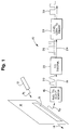
- Figure 1 illustrates a medium M which carries a bar code B previously applied thereto.
- the bar code B can be detected and converted to a binary representation thereof by means of a known read system 10.
- the system 10 includes a source of radiant energy 12.
- the source 12 is used to generate a beam of radiant energy R I , which could be monochromatic, and to direct that beam R I on to a predetermined region of a read area.
- the radiant energy R I is reflected by the elements of the bar code B, thereby forming a modulated, reflected beam of radiant energy R F .
- the beam R F is directed to a radiant energy sensor 16.
- the sensor 16 could be a photodiode, for example, a phototransistor, or other photo-sensitive device.
- Output from the sensor 16 on a conductor or a line 18 is a modulated, analog, electrical signal 20 which is representative of the elements of the bar code B.
- the analog signal 20 is coupled to a discriminator circuit 22.
- Known discriminator circuits include amplitude comparators, as well as various types of differentiators.
- the signal 26 could be coupled to a converter 28 for purposes of generating a digitized representation 30 of the modulated analog signal 20 at logic voltage levels.
- noise One problem associated with bar code reading circuitry is noise, which can cause false "ones” or “zeros" in the binary output stream. Noise can be due to variations in the quality of the bar code, as well as the configuration of the read circuitry.
- printers are used to create bar codes on surfaces with some degree of roughness.
- the printer may print bars with a significant degree of Element Reflectance Nonuniformity (ERN), as defined in ANSI Standard X3.182-1990, or reflectance variation across an element.
- Sensitive detectors may interpret the nonuniformity as additional bar or space elements, thus misreading the code.
- a granular surface on to which the codes are printed may contribute to ERN by differentially reflecting more or less light on to the detector.
- a nonuniform absorption of the printing into the surface material can also contribute to ERN.
- the bar and space element speed is high enough that the detector attenuates the amplitude of the narrow and higher frequency elements relative to the wide elements. This effect is defined as modulation in the ANSI Specification X3.192-1990 "Bar Code Print Quality - Guideline”.
- Modulation of the bar coded signal may occur when bandwidth-limited sensors are employed in bar code readers. This effect leads to elements with the same logical value, one or zero, but with differing amplitudes as the code is scanned.
- Wide elements typically have a lower frequency content than do the narrow elements, and thus, would possess higher amplitudes in the bandwidth limited systems.
- the convolution of an aperture and wide or narrow bar code elements may also contribute to higher amplitudes for wide elements relative to narrow elements.
- the rate at which the bar and space elements of a bar code symbol are sensed represents a set of frequencies to which the detector must be responsive. As the elements are sensed at higher and higher speeds, the frequency response requirements of the detector increases.
- the ERN of the wide elements is detectable as signal changes within a bar code element.
- the modulation effects are detectable as changes in amplitude between portions of the signal representative of the same logical value.
- Figure 2 is a graphical example of ERN and modulation present on the modulated analog signal 20 of Figure 1.
- the ERN noise 20a while illustrated in connection with positive peak analog values, is also present on negative peak values. Similarly, the modulation effects reduce both positive peak values, such as 20b, and increases negative peak values (not shown.)
- modulation of a bar code may be created in other ways. For a given aperture size of a sensor, there is a minimum element width which will generate a maximum signal. Bar or space elements which are narrower than this minimum will allow reflected light from adjoining elements to "leak" on to the detector, reducing the signal amplitude.
- a third method by which signal modulation may occur is by tilting a non-symmetric (that is rectangular) aperture with respect to the bar and space element edges.
- the combination of a tilted aperture across bar code element edges results in a reduced amplitude for narrow bars and spaces relative to wide bar and space amplitudes.
- the modulation need not be symmetrically placed with respect to wide bars and spaces.
- Bar code edge detectors utilizing threshold crossing or peak detection techniques are at times not capable of decoding signals with the modulation shown in Figure 2 with the desired accuracy and reliability.
- Circuits which differentiate the signal are theoretically capable of identifying each positive and negative peak where the first derivative of the input signal goes to zero.
- the output of this type of circuit is independent of the absolute signal amplitude, a differentiator is very sensitive to any high frequency noise which may be present or the signal. Hence, ERN noise can produce false "one" or "zero" pulses.
- modulation effects can modify the sensor waveform to the point that traditional element edge determination techniques do not function adequately.
- hysteresis produced by positive feedback in comparator circuits may also limit the dynamic range of bar code speeds. Large amounts of positive feedback will tend to limit the ability of a system to detect low amplitude signals, such as those generated by low bandwidth systems when exposed to high speed bar codes. At very low bar code speeds, where an unchanging input signal exists for a significant amount of time, the low hysteresis levels needed for high speed operation may not be adequate in the presence of electronic noise and the input offset voltage inherent in comparators.
- a bar code digitizing circuit must reconcile several conflicting performance requirements in order to accurately and reliably interpret an incoming waveform.
- This waveform may consist of high or low frequency constituents, ERN, modulation, overall amplitude variations, acceleration, or other undesirable modifiers to the bar coded signal.
- a slope responsive detector for producing a binary output signal corresponding to a binary information sequence carried by an analog signal having peak amplitudes of different values bounded by first and second slopes, wherein some of the amplitudes have substantially constant values
- the detector comprising: a detection circuit for detecting first and second slopes; and an output circuit coupled to the detection circuit and responsive only to the detected slopes for producing first and second binary output signals, a first binary output signal being generated when a first slope is detected and maintained in the presence of a substantially constant amplitude value until a second slope is detected whereupon a second binary output signal is generated.
- bar code reading apparatus usable to generate a binary representation of an analog signal modulated by an input sequence, comprising: a sensor for converting an input sequence to an analog signal modulated in accordance therewith; at least one truncator circuit coupled to the sensor, for substantially eliminating noise on selected peak amplitudes of the modulated signal and for forming a smoothed representation of the analog signal; and a detector, coupled to the truncator circuit, as described above.
- a device for converting an analog input signal with varying peak values and transitions to a binary output signal wherein the device includes positive and negative peak detectors with peak hold circuits coupled thereto and a comparator circuit; characterized in that each peak detector and respective peak hold circuit includes circuitry for eliminating selected of the varying peak values from the input signal; and slope sensing circuitry, coupled between the eliminating circuitry and the comparator for detecting transitions in the input signal and for generating the binary output signal therefrom.
- a second clipping circuit can be used to smooth both high or low peak values of the modulated input signal.
- the slope detecting circuit will include a tracking circuit to provide a symmetrical hysteresis characteristic.
- a system in accordance with the present invention can accurately convert an input analog signal to a binary signal over a wide dynamic range.
- the system also reliably operates in the presence of relatively long, substantially constant, peak values of the input analog signal.
- digital techniques can be used to process the modulated analog input signal.
- One or more digital signal processors can be used to implement this embodiment.
- a noise suppression or clipping circuit 40 in accordance with the present invention, is illustrated in the block diagram of Figure 3.
- the circuit 40 is coupled to the sensor 16 and receives a noisy information modulated signal, corresponding to the signal 20 shown in Figure 2, on the conductor or line 18.
- the signal 20 is coupled to an attenuator 42 and an amplifier 44. Output from the attenuator 42 is coupled to a peak detector 46 and peak hold circuitry 48.
- Outputs from the amplifier 44 and the peak hold circuit 48 are coupled via conductors or lines 44b, 48b to a voltage limiter circuit 50.
- the output from the limiter circuit 50, on a line 50b, is a non-noisy analog signal, representative of the noisy input signal 20.
- the peak hold circuitry 48 includes an RC time constant to sense and hold the maximum positive excursion of the input signal 20.
- the input signal 20 is amplified by the amplifier 44, an amount that causes all of the ERN negative going excursions to be at a higher voltage than the voltage at the output of the peak hold circuit 48.
- the peak detector 46 and peak hold circuit 48 produces the output.
- the bar code sensor senses lower amplitude elements without the ERN noise, the amplified signal from the amplifier 44 becomes the output.
- ERN noise can be eliminated for positive or negative peak values, such as 20a in Figure 2, using the circuit 40.
- the attenuator 42 may not be needed for a negative peak clipping or smoothing circuit.
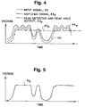
- Figure 4 is a graph illustrating various signals for the circuit of Figure 3 configured to smooth positive peak input values for the signal 20.
- Figure 5 illustrates the smoothed output 51p from the circuit 40 when so configured.
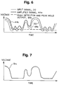
- Figures 6 and 7 illustrate waveforms associated with the smoothing circuit 40 when configured to clip and smooth negative peak values of the modulated analog signal 20.
- the output signal 51n of Figure 7 has smoothed negative peak values.
- the attenuator circuit 42 and amplifier 44 have opposite effects.
- the attenuator 42 reduces the waveform amplitude and the amplifier 44 increases the amplitude.
- the attenuator circuit 42 and amplifier circuit 44 act in the same direction, moving the waveform towards a negative voltage reference. In this case, it may be necessary to attenuate the signal more than the amplification of the negative voltage.
- the proper combination of attenuation and amplification is one where the lowest expected ERN voltage amplitude in the amplified signal is greater than the largest voltage amplitude in the attenuated signals for a bar code element.
- the output on the line 50b is the lower voltage amplitude of the two inputs.
- Figure 8 illustrates positive peak clipping circuitry 40a by which the unwanted ERN or positive peak values of the incoming signal 20 shown in Figure 2 is eliminated.
- the signal from an optical sensor 16 is input to the attenuator 42, formed of resistors 60a and 60b.
- the amplitude of the signal 20, Figure 2 is reduced by the ratio of resistor 60a to the sum of resistors 60a and 60b.
- the negative voltage reference -V r is set to ground potential. If the sensor waveform is negative, the voltage reference -V r is a fixed negative voltage of lower potential than the sensor waveform.
- the attenuated signal enters the peak detector circuit 46p.
- the positive peak detector 46p includes an operational amplifier 62a, diodes 62b, 62c, and an input resistor 62d.
- Diode 62b limits the output of amplifier 62a to voltages higher than that stored at the input of the peak hold circuit 48p.
- the diode 62c limits the output of the amplifier 62a to a maximum of one diode forward voltage drop from the stored voltage on the input to the peak hold circuit 48p.
- the positive peak hold circuit 48p contains a storage capacitor 64a and a resistor 64b referenced to -V r .
- a time constant formed by the capacitor 64a and resistor 64b allows a slow decay in voltage towards -V r relative to the rate at which bar and space elements are sensed.
- the peak hold circuitry 48p can reestablish the relative peak voltage based on recent signal levels. Otherwise, the peak hold circuit 48p is fixed at the highest voltage sensed by the peak detector circuit 46p. Any ERN voltage in the incoming waveform 20, shown in Figure 2, does not change the output of the peak hold circuit 48p.
- Amplifiers 66a and 68a along with resistors 66b and 66c, and 68b and 68c, respectively, buffer the signal from loading by other circuit elements.
- the output of the peak detector and hold circuits 46p, 48p is the maximum voltage of the attenuated output signal, slowly decaying in amplitude based on the RC time constant formed of resistor 64b and capacitor 64a. As soon as the attenuated input signal amplitude rises above the voltage on the capacitor 64a, the output of amplifier 62a quickly increases the voltage on that capacitor to be equal to the amplifier input. The output of the peak detector and peak hold circuits on a line 49p thus rises quickly and falls slowly.
- the sensor waveform on the line 18 is also input to amplifier circuit 44.
- the amplifier circuit 44 includes an operational amplifier 70a, input resistor 70b, and feedback resistors 70c, 70d. It is the proper selection of attenuation in the circuit 42 and amplification in the circuit 44 which suppresses the unwanted ERN voltage.
- the gain of this circuit is equal to one plus the ratio of the resistor 70c to the resistor 70d.
- the output from the amplifier circuit 44 and the peak hold circuit 48p are connected to a voltage limiter circuit 50p.
- the limiter circuit 50p includes a resistor 72a and a diode 72b.
- the output of the limiter 50p on line 51p is the higher voltage of the two input lines 49p and 44p.
- a differentiator or other circuitry can be employed to determine bar and space edges. This edge determination process can convert the waveform into digital levels as a function of time for subsequent decoding.
- Figure 9 is a schematic of a negative peak clipping and smoothing circuit 40b by which the unwanted ERN on negative peak values of the incoming signal can be eliminated. Because of changes in the connectivity of the negative peak detector 46n and negative peak hold circuit 48n, the attenuator 42 shown in Figure 8 has been be eliminated from the negative peak smoothing circuit 40b.
- the signal from an optical sensor 16 is input to the negative peak detector circuit 46n on line 18.
- That circuit includes an amplifier 82a, an output diode 82b, feedback diode 82c and resistor 82d, and an input resistor 82e.
- the diode 82b restricts the amplifier 82a to outputting only voltages lower than that on the input of the peak hold circuit 48n.
- Diode 82c maintains the output of amplifier 82a a maximum of one diode forward voltage drop from the voltage on the input to the negative peak hold circuit 48n.
- the negative peak hold circuit 48n includes an input RC time constant circuit, with capacitor 84a, and resistor 84b, coupled to an operational amplifier 86a through an input resistor 86b.
- the resistor 86c provides a feedback path and the resistor 86d provides a negative input for the operational amplifier 86a.
- Output from the amplifier 86a is coupled to a buffer output amplifier 88a via an input resistor 88b in buffer circuit 24.
- a feedback resistor 88c is coupled between the output 48n and the inverted input of the amplifier 88a.
- the capacitor 84a and resistor 84b are coupled to a positive voltage +V r .
- +V r is set to ground potential.
- +V r is set to a level which is higher than the highest expected voltage of any negative excursion of the incoming signal plus the ERN.
- the time constant formed by the capacitor 84a and resistor 84b allows a slow decay in voltage towards the +V r relative to the rate at which bar and space elements are sensed.
- the peak hold circuitry 48n can reestablish the relative peak voltage based on recent signal levels. Otherwise, the peak hold circuit is fixed at the lowest voltage sensed by the negative peak detector circuit 46n. Any ERN voltage in the incoming waveform does not change the output of the peak hold circuit 48n.
- the peak detector circuit 46n and the peak hold circuit 48n together provide an overall gain factor for the input signal.
- the circuits are configured such that if the ratio of resistor 82e to resistor 82d is equal to the ratio of resistor 86c to resistor 86d, the gain of the two circuits is equal to:
- the output of the negative peak hold circuit 48n is the value of the minimum voltage of the input signal times the gain. This value slowly rises in amplitude towards +V r based on the time constant of capacitor 84a and resistor 84b.
- the output of amplifier 82a quickly restores the voltage on the capacitor 84a to be equal to the amplified input.
- the output of the negative peak hold circuit 48n falls quickly and rises slowly.
- the sensor waveform is input to the amplifier circuit 44.
- the amplifier circuit 44 is as described with reference to Figure 8. The proper selection of amplification in circuit 44 relative to the amplification formed by circuits 46n and 48n, suppresses the unwanted ERN voltage.
- the gain of the circuit is equal to one plus the ratio of the resistor 70c to the resistor 70d.
- the proper amplification levels are where the highest expect ERN voltage in the amplified signal from circuit 44 is lower than the lowest voltage produced by circuits 46n and 48n.
- the output of the negative peak detector 46n and hold circuits 48n on line 49n, and the output of the amplifier 44 on line 44n are connected to the voltage limiter circuit 50n.
- the voltage limiter circuit 50n includes a resistor 92a and a diode 92b, Figure 9.
- the output of the limiter 50n on the line 51n is the higher voltage of the two input lines 44n and 49n.
- Figure 6 illustrates the output on the line 49n of the negative peak detector and hold circuitry 46n, 48n, and the output on the line 44n of the amplifier 44 in relation to the sensor input waveform.
- Figure 7 illustrates how the voltage limiter circuit 50n alternately chooses which of the two inputs drives the output signal on the line 51n, depending upon the relative magnitudes.
- the detector 100 can be used to detect bar code elements moving over a wide range of velocities and is insensitive to modulation and small amplitude, high frequency noise.
- a comparator 102 and first and second RC circuits 104a, 104b are configured such that the output of the detector 100 is determined by the sign of the difference of the first derivative of the voltage signals at inputs 102a, 102b to the comparator 102.
- the output of the detector 100 on a line 102c is one of two discrete voltage values which, if not already digital 5 volts and 0 volts, can easily be converted into such.
- the detector 100 has an input line 104c coupled to the circuits 104a, 104b.
- the circuit 104a includes a resistor 106a and a capacitor 106b.
- the circuit 104b includes a resistor 108a and a capacitor 108b.
- V0 A sgn [(V+) - (V-)] (1)
- A is the amplitude of the output signal V+ is the voltage at the positive input 102a of the comparator 102
- V- is the voltage at the negative input 102b of the comparator 102
- V0 A sgn[ ⁇ lO4b * (V-)'- ⁇ lO4a * (V+)'] (2)
- a feedback resistor 109 is used to create a small amount of hysteres
- Proper bar code element detection is achieved by the detector 100 when the RC time constant ⁇ 104a formed by the resistor 106a and capacitor 106b, is smaller than the RC time constant ⁇ 104b formed by the resistor 108a and the capacitor 108b. With this arrangement, the voltage signal on the capacitor 106b will phase lead the signal on the capacitor 108b.
- the voltage signal input on the line 104c will peak high or low. The input signal then move from that peak value towards an opposite peak.
- the selection of the ratio between ⁇ 104a and ⁇ 104b is a trade-off between increased sensitivity to bar and space peaks, and immunity from unwanted transitions caused by noise. As the ratio increases, (V+)' must be larger and larger than (V-)' in order to change the comparator output. In this manner, the excess sensitivity to high frequency noise, characteristic of differentiator circuits is avoided.
- equation (2) does not contain any terms relative to the signal amplitude, the detector 100 is insensitive to the effects of modulation. Only the derivative input signals (V+)' and (V-)' determine the output V0.
- the positive feedback formed by the inclusion of resistor 109 acts to suppress unwanted output changes caused by noise, or oscillation of the comparator.
- the amount of hysteresis is determined by resistors 106a and 109.
- the hysteresis voltage serves to assure that when ⁇ 104a * (V+)' approaches ⁇ 104b * (V-)', only one transition of V0 (as opposed to several, which can be caused by the influence of noise) occurs.
- hysteresis is provided in the detector 100 by connecting resistor 109 between the output 102c from comparator 102 and the positive input 102a.
- resistor 109 may result in a non-symmetrical hysteresis condition.
- the hysteresis will not be symmetric with respect to the signal level V0.
- a greater positive feedback voltage must be overcome in order to change the output in one direction than is required to change in the other direction.
- the asymmetric hysteresis condition mentioned above may limit the operation of the slope detector circuit 100. For example, if the smaller of the two hysteresis voltages is scaled for the expected input waveform, some small bar or space features may not generate a (V+)' or (V-)', large enough to cause a state change in the comparator 102.
- the reduced noise immunity of the smaller hysteresis may result in unwanted output changes and bar code misreads. In either case, the reduced sensitivity or lower noise immunity can result in lower performance of the detector 100.
- a resistor connected between the comparator output and a positive voltage source, pulls the signal to its "high" level. If there are amplitude changes in the positive voltage source due to current loading by another device sharing the source, noise generated by or conducted into the voltage source (or other phenomena), V0 variation results in changes in hysteresis voltage.
- the asymmetrical voltages and the V0 amplitude sensitivity serve to limit the performance of the slope detector 100 in some circumstances.
- a tracking hysteresis circuit can be used instead of the resistor 109.
- Figure 12 illustrates another circuit 100a with a feedback circuit 109a, which provides a symmetric hysteresis characteristic and is sensitive to comparator output amplitudes.
- the detector 100 as described above is incorporated into the circuit 100a of Figure 12. Components already described are referenced alike and will not be described again here.
- the feedback amplifier circuit 109a tracks the input signal on the line 104c and to regulate the hysteresis symmetrically with respect thereto. In this manner, the positive and negative hysteresis values will be equal, and will not be influenced by changes in V0.
- the circuit 109a includes an operational amplifier 120, resistors 122a and 122b, diodes 124a and 124b, and resistors 126a and 126b.
- the operational amplifier 120 has been configured as a buffer, with the output of the device on a line 120a equal to the voltage at its positive input terminal 120b.
- the input 120b is connected to the input signal on the line 104c through the input resistor 122a.
- the diodes 124a and 124b clamp the voltage at node 124c to a value equal to the input signal ⁇ one diode forward voltage drop (that is about 0.7V).
- the output of the comparator of the detector 100a is given by equation (1). If the current flow into the inputs of the comparator 102 is negligible, and the output voltage V0 for the detector 100a can be expressed as:
- the hysteresis voltage given by is no longer a function of V0. It is determined by the ratio of resistors R106a and R126a, and the forward voltage drop V D of the respective diode 124a or 124b. The hysteresis voltage amplitude is thus independent of whether the output V0 is "high” or "low".
- This symmetric hysteresis characteristic permits a choice of the ratio of resistors which, when multiplied by the diode forward voltage drop V D , is large enough to suppress unwanted transitions. This value is still small enough to allow small but valid changes in (V+)' and (V-)' to be sensed as bar and space elements, thereby increasing the performance range of the detector 100a over that of the detector 100.
- the output V0 of the detector 100a is not a function of the input signal level, but of the first derivative of the voltages on the inputs 102a, 102b of the comparator 102.
- the advantages of the insensitivity to modulation or amplitude variation are preserved in the detector 100a.
- the previously discussed modules can be combined to form an improved bar code digitizing system 140, in accordance with the present invention.
- the system 140 as described subsequently, can detect and properly digitize high and low speed bar coded signals that have been converted to a modulated analog voltage, such as the voltage 20 of Figure 2.
- the circuit 140 includes positive and negative peak clipping circuits 142, 144, which are similar structurally and functionally to the positive and negative peak smoothing circuits 40a and 40b of Figures 8 and 9.
- the clippers 142, 144 share a common gain stage 44.
- the clipper circuits 142, 144 in combination with the gain stage 44, flatten the ERN voltage, such as the ERN voltage 20a of Figure 2, thereby forming a composite, processed representation 21 of the input modulated analog signal 20.
- the processed analog signal 21, illustrated in Figure 13, on a line 21a, is then input to a slope detector circuit 100b, similar to the detector 100a.
- the output signal V0 from the detector 100b can then be translated, if needed, to logic levels in a translator or shifter circuit 146 to produce a binary output signal V out .
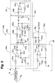
- Figure 14 is a schematic of the system 140.
- elements which were previously described in connection with Figures 8, 9, and 12 have been given the same identification numerals, and need not be discussed further.
- the input signal 20, Figure 2 from the bar code sensor 16 is input on line 18 into the three subcircuits, the positive peak clipper 142, the negative peak clipper 144, and the gain amplifier 44.
- the positive peak clipper attenuator, formed by resistors 60a and 60b, and the gain of the negative peak clipper 144 are matched to the gain in circuit 44 such that all the ERN on the highest and lowest amplitude elements, such as 20a, Figure 2, is higher or lower than the respective peak levels of the input signal 20, Figure 2.
- the peak clipping circuits 142, 144 do not affect modulation per se, but smooth or flatten the tops and bottoms of the highest and lowest amplitude elements.
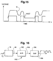
- Figure 15 illustrates the effects of conditioning the input signal 20 of Figure 2 with the positive and negative peak clipping circuits 142, 144, thereby producing a processed noise-free representation 21 thereof.
- Resistors 150a and 150b have been added to the slope detecting circuit 100b of Figure 14.
- the output of the detector 100b is given by equation (1).
- resistor 126a For proper operation, the value of resistor 126a must be greater than the value of resistor 150a, such that: R126a + R150a ⁇ R126a and There are two cases to consider.
- the output of the gain stage 44 When the output of the gain stage 44 is higher than the positive peak clipper voltage output, or lower than the negative peak clipper output, the active peak clipper voltage establishes the input at resistor 108a.
- the gain output sets the voltage for the negative input to the slope detector 100b. Case A will refer to the circumstance where circuit 44 sets the voltage; and Case B will refer to the case where a peak clipper circuit output sets the slope detector input level.
- the output of the slope detector 100b is:
- Cases A and B represent the expected behavior for the circuit 140.
- the term is small, being retained since it represents the hysteresis voltage on the slope detector.
- V pc is the voltage level but has of the active peak clipper circuit and
- V g is the voltage output from the gain circuit 44. The system accurately decodes a high or low speed, distorted signal as is described below.
- the positive feedback term of ( ⁇ V d R106a/R126a) is small in magnitude so that low amplitude bar and space edges can generate a (V+)' and (V-)' large enough to change the sign of V0.
- the small amount of hysteresis is sufficient to keep the comparator 102 from oscillating at those points in a time when (V+)' and (V-)' are very close in magnitude.
- V pc - V g the (V pc - V g ) term increases the effective noise suppression.
- this extra term disappears, allowing small amplitude elements to be detectable.
- the slope detector 100b can detect high speed, highly modulated bar code elements. It can also properly decode very slow, very flat waveform elements.
- the tracking hysteresis circuit 109a requires that the output levels of the slope detector 100b be higher than the highest input voltage from the sensor 16, and lower than the lowest input voltage therefrom. That often means that the slope detector output levels are not digital commonly used +5 volt and zero volt voltages.
- Translator circuit 146 can be used to make a voltage conversion.
- Circuit 146 includes a comparator 160, resistors 162, 164, 166, 168, and schottky diode 170.
- the circuit 146 can be used to convert the output levels V0 of the slope detector into digital one and digital "zero" voltages, corresponding to the binary output voltage V out of Figure 15.
- improved tracking can be achieved in the system 140 by open circuiting a region 18a of the conductor 18, as illustrated in Figure 14.
- a connection 18b illustrated in phantom in Figure 14, is provided between the resistor 60a and the output line 21a.
- comparators can be integrated voltage comparators, type LM339AM.
- Operational amplifiers can be LM324AM-type integrated circuits.
- the present invention includes alternate processing techniques.
- the output 20 from the sensor 16 could be digitally processed in digital processing chips.
- Figure 16 is a block diagram of a digital system 190 in accordance with the present invention.
- the digital system 190 digitizes the output signal 20, Figure 2, from the sensor 16 on line 18 in an analog-to-digital converter 192.
- the digital values, on a line or lines 194, are coupled to one or more digital signal processing chips 196.
- the chips are configured to digitally process the input signal 20, Figure 2, in accordance with the above described techniques.
- the output from the signal processor 196, on a line 198, is a digitized representation of the modulated analog input signal 20, Figure 2.
- the output on the line 198 corresponds to the output V out on the line 172 of Figure 14, but is achieved by digital rather than analog processing.
Abstract
Description
- The invention pertains to circuitry for detecting bar codes carried on a medium and for generating binary representations thereof. More particularly, the invention pertains to circuits which smooth or clip peak values of a bar code modulated analog signal and which detect slopes therein.
- The use of bar codes to identify products, documents, or other media, or to specify characteristics thereof, has become very common. Bar codes can improve the speed and accuracy of information transfer. Unfortunately, the increase in bar code use has led to difficulties in read accuracy and reliability.
- In known read systems, a source is usually used to generate a beam of radiant energy which is directed on to the bar code, usually by moving a bar coded medium through a read station. A photodetector is used to detect radiant energy reflected off of the moving bar code.
- The photodetector produces a bar code modulated analog signal in response to reflected radiant energy. The modulated analog signal, which can have high and low amplitudes corresponding to the bar and space elements of the bar code, is then converted to a binary representation of the bar coded information.
- For a further understanding of the problem, Figure 1 illustrates a medium M which carries a bar code B previously applied thereto. The bar code B can be detected and converted to a binary representation thereof by means of a known
read system 10. - The
system 10 includes a source ofradiant energy 12. Thesource 12 is used to generate a beam of radiant energy RI, which could be monochromatic, and to direct that beam RI on to a predetermined region of a read area. - As the medium M and associated bar code B move in a
direction 14 past the predefined region, the radiant energy RI is reflected by the elements of the bar code B, thereby forming a modulated, reflected beam of radiant energy RF. The beam RF is directed to aradiant energy sensor 16. Thesensor 16 could be a photodiode, for example, a phototransistor, or other photo-sensitive device. - Output from the
sensor 16 on a conductor or aline 18 is a modulated, analog,electrical signal 20 which is representative of the elements of the bar code B. Theanalog signal 20 is coupled to adiscriminator circuit 22. Known discriminator circuits include amplitude comparators, as well as various types of differentiators. - The output signal from the
discriminator circuit 22 on aline 24, which might be, for example, a bi-valued voltage, +V and -V, is a representation of the modulatedanalog signal 26. Thesignal 26 could be coupled to aconverter 28 for purposes of generating adigitized representation 30 of the modulatedanalog signal 20 at logic voltage levels. - One problem associated with bar code reading circuitry is noise, which can cause false "ones" or "zeros" in the binary output stream. Noise can be due to variations in the quality of the bar code, as well as the configuration of the read circuitry.
- In many applications, inexpensive printers are used to create bar codes on surfaces with some degree of roughness. The printer may print bars with a significant degree of Element Reflectance Nonuniformity (ERN), as defined in ANSI Standard X3.182-1990, or reflectance variation across an element. Sensitive detectors may interpret the nonuniformity as additional bar or space elements, thus misreading the code.
- A granular surface on to which the codes are printed may contribute to ERN by differentially reflecting more or less light on to the detector. A nonuniform absorption of the printing into the surface material can also contribute to ERN.
- Another problem associated with known bar code reading circuits is inaccuracy caused by limited dynamic range of the read circuitry. As a result, that circuitry is unable to discriminate relatively high frequency bar coded elements. This in turn imposes limitations on the velocity at which the bar coded medium M can move through the read station, as well as the range of velocity variations of the medium M that can be tolerated by the read circuitry.
- Often, the bar and space element speed is high enough that the detector attenuates the amplitude of the narrow and higher frequency elements relative to the wide elements. This effect is defined as modulation in the ANSI Specification X3.192-1990 "Bar Code Print Quality - Guideline".
- Modulation of the bar coded signal may occur when bandwidth-limited sensors are employed in bar code readers. This effect leads to elements with the same logical value, one or zero, but with differing amplitudes as the code is scanned.
- Wide elements typically have a lower frequency content than do the narrow elements, and thus, would possess higher amplitudes in the bandwidth limited systems. The convolution of an aperture and wide or narrow bar code elements may also contribute to higher amplitudes for wide elements relative to narrow elements.
- The rate at which the bar and space elements of a bar code symbol are sensed represents a set of frequencies to which the detector must be responsive. As the elements are sensed at higher and higher speeds, the frequency response requirements of the detector increases.
- The ERN of the wide elements is detectable as signal changes within a bar code element. The modulation effects are detectable as changes in amplitude between portions of the signal representative of the same logical value. Figure 2 is a graphical example of ERN and modulation present on the modulated
analog signal 20 of Figure 1. - In the
waveform 20, theERN noise 20a, while illustrated in connection with positive peak analog values, is also present on negative peak values. Similarly, the modulation effects reduce both positive peak values, such as 20b, and increases negative peak values (not shown.) - In addition to the effects of bandwidth-limited sensors, modulation of a bar code may be created in other ways. For a given aperture size of a sensor, there is a minimum element width which will generate a maximum signal. Bar or space elements which are narrower than this minimum will allow reflected light from adjoining elements to "leak" on to the detector, reducing the signal amplitude.
- A third method by which signal modulation may occur is by tilting a non-symmetric (that is rectangular) aperture with respect to the bar and space element edges. The combination of a tilted aperture across bar code element edges results in a reduced amplitude for narrow bars and spaces relative to wide bar and space amplitudes.
- As seen in Figure 2, the modulation need not be symmetrically placed with respect to wide bars and spaces. Bar code edge detectors utilizing threshold crossing or peak detection techniques are at times not capable of decoding signals with the modulation shown in Figure 2 with the desired accuracy and reliability.
- Circuits which differentiate the signal are theoretically capable of identifying each positive and negative peak where the first derivative of the input signal goes to zero. Although the output of this type of circuit is independent of the absolute signal amplitude, a differentiator is very sensitive to any high frequency noise which may be present or the signal. Hence, ERN noise can produce false "one" or "zero" pulses.
- Additionally, modulation effects can modify the sensor waveform to the point that traditional element edge determination techniques do not function adequately.
- The use of hysteresis produced by positive feedback in comparator circuits may also limit the dynamic range of bar code speeds. Large amounts of positive feedback will tend to limit the ability of a system to detect low amplitude signals, such as those generated by low bandwidth systems when exposed to high speed bar codes. At very low bar code speeds, where an unchanging input signal exists for a significant amount of time, the low hysteresis levels needed for high speed operation may not be adequate in the presence of electronic noise and the input offset voltage inherent in comparators.
- Therefore, a bar code digitizing circuit must reconcile several conflicting performance requirements in order to accurately and reliably interpret an incoming waveform. This waveform may consist of high or low frequency constituents, ERN, modulation, overall amplitude variations, acceleration, or other undesirable modifiers to the bar coded signal.
- Thus, there continues to be a problem in providing accurate, noise insensitive read circuitry with substantial bandwidth. Preferably, such circuitry will be inexpensive and readily manufacturable.
- In accordance with one aspect of the present invention, there is provided a slope responsive detector for producing a binary output signal corresponding to a binary information sequence carried by an analog signal having peak amplitudes of different values bounded by first and second slopes, wherein some of the amplitudes have substantially constant values, the detector comprising:
a detection circuit for detecting first and second slopes; and
an output circuit coupled to the detection circuit and responsive only to the detected slopes for producing first and second binary output signals, a first binary output signal being generated when a first slope is detected and maintained in the presence of a substantially constant amplitude value until a second slope is detected whereupon a second binary output signal is generated. - In accordance with a second aspect of the present invention, there is provided bar code reading apparatus, usable to generate a binary representation of an analog signal modulated by an input sequence, comprising:
a sensor for converting an input sequence to an analog signal modulated in accordance therewith;
at least one truncator circuit coupled to the sensor, for substantially eliminating noise on selected peak amplitudes of the modulated signal and for forming a smoothed representation of the analog signal; and
a detector, coupled to the truncator circuit, as described above. - In accordance with a third aspect of the present invention, there is provided a device for converting an analog input signal with varying peak values and transitions to a binary output signal wherein the device includes positive and negative peak detectors with peak hold circuits coupled thereto and a comparator circuit;
characterized in that each peak detector and respective peak hold circuit includes circuitry for eliminating selected of the varying peak values from the input signal; and
slope sensing circuitry, coupled between the eliminating circuitry and the comparator for detecting transitions in the input signal and for generating the binary output signal therefrom. - In accordance with a fourth aspect of the present invention, there is provided a method of detecting information carried by an analog signal having at least some peak amplitudes of substantially constant value, bounded by first and second slopes of different signs, the method comprising the steps of:
- a) sensing the analog signal;
- b) detecting the first and second slopes independent of amplitude values;
- c) initiating a first binary output value only in response to detecting a first slope, and maintaining that first binary output value in the presence of a subsequent substantially constant amplitude value until a second slope is detected; and
- d) initiating a second binary output value, only in response to detecting the second slope, and maintaining that second binary output value in the presence of a subsequent substantially constant amplitude value until a first slope is detected.
- A second clipping circuit can be used to smooth both high or low peak values of the modulated input signal. Preferably, the slope detecting circuit will include a tracking circuit to provide a symmetrical hysteresis characteristic.
- A system in accordance with the present invention can accurately convert an input analog signal to a binary signal over a wide dynamic range. The system also reliably operates in the presence of relatively long, substantially constant, peak values of the input analog signal.
- Alternately, digital techniques can be used to process the modulated analog input signal. One or more digital signal processors can be used to implement this embodiment.
- For a better understanding of the present invention, reference will now be made, by way of example only, to the accompanying drawings in which:-
- Figure 1 is a block diagram of known bar code read circuitry;
- Figure 2 is a graph of modulated analog voltage for the circuitry of Figure 1 as a function of time;
- Figure 3 is a block diagram of a clipping circuit in accordance with the present invention;
- Figure 4 is a graph of an input and internal signals for a positive clipping circuit as illustrated in Figure 3 as a function of time;
- Figure 5 is graph of the output of a positive clipping circuit in accordance with Figure 3, in response to the input signal of Figure 4 as a function of time;
- Figure 6 is a graph of an input and internal signals for a negative clipping circuit as in Figure 3 as a function of time;
- Figure 7 is a graph of the output of a negative clipping circuit in accordance with Figure 3, in response to the input signal of Figure 6 as a function of time;
- Figure 8 is a schematic of the circuit of Figure 3 configured to clip and smooth positive peak values of an input signal;
- Figure 9 is a schematic diagram of the circuit of Figure 3 configured to clip and smooth negative peak values of an input signal;
- Figure 10 is a schematic diagram of a slope detector in accordance with the present invention;
- Figure 11 is a graph of input and output waveforms of the detector of Figure 10 as a function of time;
- Figure 12 is a schematic of an improved slope detector in accordance with the present invention;
- Figure 13 is a block diagram of a bar code digitizing system in accordance with the present invention;
- Figure 14 is a schematic diagram of the digitizing system of Figure 13;
- Figure 15 is a graph of various signals of the circuit of Figure 14 as a function of time; and
- Figure 16 is a block diagram of an alternate digital embodiment in accordance with the present invention.
- While this invention is susceptible of embodiment in many different forms, there are shown in the drawings, and will be described herein in detail, specific embodiments thereof with the understanding that the present disclosure is to be considered as an exemplification of the principles of the invention and is not intended to limit the invention to the specific embodiments illustrated.
- A noise suppression or clipping
circuit 40, in accordance with the present invention, is illustrated in the block diagram of Figure 3. Thecircuit 40 is coupled to thesensor 16 and receives a noisy information modulated signal, corresponding to thesignal 20 shown in Figure 2, on the conductor orline 18. - The
signal 20 is coupled to anattenuator 42 and anamplifier 44. Output from theattenuator 42 is coupled to apeak detector 46 andpeak hold circuitry 48. - Outputs from the
amplifier 44 and thepeak hold circuit 48 are coupled via conductors orlines voltage limiter circuit 50. The output from thelimiter circuit 50, on aline 50b, is a non-noisy analog signal, representative of thenoisy input signal 20. - The
peak hold circuitry 48 includes an RC time constant to sense and hold the maximum positive excursion of theinput signal 20. In addition, theinput signal 20 is amplified by theamplifier 44, an amount that causes all of the ERN negative going excursions to be at a higher voltage than the voltage at the output of thepeak hold circuit 48. - Only the lower voltage signal of the
peak hold circuit 48 on theline 48b, or the output of theamplifier 44 on theline 44b, is output from thelimiter 50, on theline 50b. Hence, the ERN noise can be eliminated from the output signal online 50b. - Thus, when a wide, large amplitude element with ERN noise is being detected, the
peak detector 46 andpeak hold circuit 48 produces the output. When the bar code sensor senses lower amplitude elements without the ERN noise, the amplified signal from theamplifier 44 becomes the output. - ERN noise can be eliminated for positive or negative peak values, such as 20a in Figure 2, using the
circuit 40. Theattenuator 42 may not be needed for a negative peak clipping or smoothing circuit. - Figure 4 is a graph illustrating various signals for the circuit of Figure 3 configured to smooth positive peak input values for the
signal 20. Figure 5 illustrates the smoothedoutput 51p from thecircuit 40 when so configured. - Figures 6 and 7 illustrate waveforms associated with the smoothing
circuit 40 when configured to clip and smooth negative peak values of the modulatedanalog signal 20. The output signal 51n of Figure 7 has smoothed negative peak values. - For voltage signals from the
sensor 16 which are positive, theattenuator circuit 42 andamplifier 44 have opposite effects. Theattenuator 42 reduces the waveform amplitude and theamplifier 44 increases the amplitude. - For signals from the
sensor 16 which are negative, theattenuator circuit 42 andamplifier circuit 44 act in the same direction, moving the waveform towards a negative voltage reference. In this case, it may be necessary to attenuate the signal more than the amplification of the negative voltage. - For either positive or negative peak signals, the proper combination of attenuation and amplification is one where the lowest expected ERN voltage amplitude in the amplified signal is greater than the largest voltage amplitude in the attenuated signals for a bar code element. When the output of the positive peak detector and hold
circuits amplifier 44 are connected to thevoltage limiter circuit 50, the output on theline 50b is the lower voltage amplitude of the two inputs. - Figure 8 illustrates positive
peak clipping circuitry 40a by which the unwanted ERN or positive peak values of theincoming signal 20 shown in Figure 2 is eliminated. The signal from anoptical sensor 16 is input to theattenuator 42, formed ofresistors signal 20, Figure 2, is reduced by the ratio ofresistor 60a to the sum ofresistors - If the sensor voltage waveform is positive, the negative voltage reference -Vr is set to ground potential. If the sensor waveform is negative, the voltage reference -Vr is a fixed negative voltage of lower potential than the sensor waveform.
- The attenuated signal enters the
peak detector circuit 46p. Thepositive peak detector 46p includes anoperational amplifier 62a,diodes input resistor 62d. -
Diode 62b limits the output ofamplifier 62a to voltages higher than that stored at the input of thepeak hold circuit 48p. Thediode 62c limits the output of theamplifier 62a to a maximum of one diode forward voltage drop from the stored voltage on the input to thepeak hold circuit 48p. - The positive
peak hold circuit 48p contains astorage capacitor 64a and aresistor 64b referenced to -Vr. A time constant formed by thecapacitor 64a andresistor 64b allows a slow decay in voltage towards -Vr relative to the rate at which bar and space elements are sensed. - Thus, if the overall signal level changes as a bar code is scanned due to reflectance or other optical variations, the
peak hold circuitry 48p can reestablish the relative peak voltage based on recent signal levels. Otherwise, thepeak hold circuit 48p is fixed at the highest voltage sensed by thepeak detector circuit 46p. Any ERN voltage in theincoming waveform 20, shown in Figure 2, does not change the output of thepeak hold circuit 48p. -
Amplifiers resistors - The output of the peak detector and hold
circuits resistor 64b andcapacitor 64a. As soon as the attenuated input signal amplitude rises above the voltage on thecapacitor 64a, the output ofamplifier 62a quickly increases the voltage on that capacitor to be equal to the amplifier input. The output of the peak detector and peak hold circuits on aline 49p thus rises quickly and falls slowly. - The sensor waveform on the
line 18 is also input toamplifier circuit 44. Theamplifier circuit 44 includes anoperational amplifier 70a,input resistor 70b, andfeedback resistors circuit 42 and amplification in thecircuit 44 which suppresses the unwanted ERN voltage. The gain of this circuit is equal to one plus the ratio of theresistor 70c to theresistor 70d. - The output from the
amplifier circuit 44 and thepeak hold circuit 48p are connected to a voltage limiter circuit 50p. The limiter circuit 50p includes a resistor 72a and adiode 72b. The output of the limiter 50p online 51p is the higher voltage of the twoinput lines - With the undesirable ERN eliminated, a differentiator or other circuitry can be employed to determine bar and space edges. This edge determination process can convert the waveform into digital levels as a function of time for subsequent decoding.
- Figure 9 is a schematic of a negative peak clipping and smoothing
circuit 40b by which the unwanted ERN on negative peak values of the incoming signal can be eliminated. Because of changes in the connectivity of thenegative peak detector 46n and negativepeak hold circuit 48n, theattenuator 42 shown in Figure 8 has been be eliminated from the negativepeak smoothing circuit 40b. - The signal from an
optical sensor 16 is input to the negativepeak detector circuit 46n online 18. That circuit includes anamplifier 82a, anoutput diode 82b,feedback diode 82c andresistor 82d, and aninput resistor 82e. - The
diode 82b restricts theamplifier 82a to outputting only voltages lower than that on the input of thepeak hold circuit 48n.Diode 82c maintains the output ofamplifier 82a a maximum of one diode forward voltage drop from the voltage on the input to the negativepeak hold circuit 48n. - The negative
peak hold circuit 48n includes an input RC time constant circuit, withcapacitor 84a, andresistor 84b, coupled to anoperational amplifier 86a through aninput resistor 86b. Theresistor 86c provides a feedback path and theresistor 86d provides a negative input for theoperational amplifier 86a. - Output from the
amplifier 86a is coupled to abuffer output amplifier 88a via aninput resistor 88b inbuffer circuit 24. Afeedback resistor 88c is coupled between theoutput 48n and the inverted input of theamplifier 88a. Thecapacitor 84a andresistor 84b are coupled to a positive voltage +Vr. - If the incoming waveform is negative +Vr is set to ground potential. For positive voltage waveforms, +Vr is set to a level which is higher than the highest expected voltage of any negative excursion of the incoming signal plus the ERN.
- The time constant formed by the
capacitor 84a andresistor 84b allows a slow decay in voltage towards the +Vr relative to the rate at which bar and space elements are sensed. Thus, if the overall input signal level changes as a bar code is scanned due to reflectance or other optical variations, thepeak hold circuitry 48n can reestablish the relative peak voltage based on recent signal levels. Otherwise, the peak hold circuit is fixed at the lowest voltage sensed by the negativepeak detector circuit 46n. Any ERN voltage in the incoming waveform does not change the output of thepeak hold circuit 48n. - The
peak detector circuit 46n and thepeak hold circuit 48n together provide an overall gain factor for the input signal. When the circuits are configured such that if the ratio ofresistor 82e toresistor 82d is equal to the ratio ofresistor 86c toresistor 86d, the gain of the two circuits is equal to:
The voltage follower,amplifier 88a, andresistors - The output of the negative
peak hold circuit 48n is the value of the minimum voltage of the input signal times the gain. This value slowly rises in amplitude towards +Vr based on the time constant ofcapacitor 84a andresistor 84b. - As soon as the input signal amplitude drops below the stored voltage on the
capacitor 84a, the output ofamplifier 82a quickly restores the voltage on thecapacitor 84a to be equal to the amplified input. As a result, the output of the negativepeak hold circuit 48n falls quickly and rises slowly. - In addition to the negative peak detector and hold
circuits amplifier circuit 44. Theamplifier circuit 44 is as described with reference to Figure 8. The proper selection of amplification incircuit 44 relative to the amplification formed bycircuits resistor 70c to theresistor 70d. - For either positive or negative signals, the proper amplification levels are where the highest expect ERN voltage in the amplified signal from
circuit 44 is lower than the lowest voltage produced bycircuits - The output of the
negative peak detector 46n and holdcircuits 48n online 49n, and the output of theamplifier 44 online 44n are connected to thevoltage limiter circuit 50n. Thevoltage limiter circuit 50n includes aresistor 92a and adiode 92b, Figure 9. The output of thelimiter 50n on the line 51n is the higher voltage of the twoinput lines - Figure 6 illustrates the output on the
line 49n of the negative peak detector and holdcircuitry line 44n of theamplifier 44 in relation to the sensor input waveform. Figure 7 illustrates how thevoltage limiter circuit 50n alternately chooses which of the two inputs drives the output signal on the line 51n, depending upon the relative magnitudes. - Subsequent to removing ERN noise using the smoothing circuits of Figures 8 and 9, a determination must be made as to which portions of the smoothed signal should be represented as binary "one" or binary "zero" value. This determination preferably will be made using an
edge detector 100, in accordance with the present invention, as illustrated in Figure 10. - The
detector 100 can be used to detect bar code elements moving over a wide range of velocities and is insensitive to modulation and small amplitude, high frequency noise. Acomparator 102 and first andsecond RC circuits detector 100 is determined by the sign of the difference of the first derivative of the voltage signals atinputs 102a, 102b to thecomparator 102. - This arrangement incorporates the advantage of absolute amplitude insensitivity without the excessive noise sensitivity of a differentiator circuit. The output of the
detector 100 on aline 102c is one of two discrete voltage values which, if not already digital 5 volts and 0 volts, can easily be converted into such. - The
detector 100 has aninput line 104c coupled to thecircuits circuit 104a includes aresistor 106a and acapacitor 106b. Thecircuit 104b includes a resistor 108a and acapacitor 108b. - The output voltage (1/0) on the
line 102c is given by:

Where:
A is the amplitude of the output signal
V+ is the voltage at the positive input 102a of thecomparator 102
V- is the voltage at thenegative input 102b of thecomparator 102
sgn(x) is the sign function of x,
sgn(x) = 1, x≧0
sgn(x) = -1, x<0
Then:

Where:
(V+)' is the first derivative with respect to time of the input voltage signal V+
(V-)' is the first derivative with respect to time of the input voltage signal V-


Afeedback resistor 109 is used to create a small amount of hysteresis in thedetector 100. This feedback increases circuit stability in the presence of electrical noise. Consequently, the resistance value R109 of theresistor 109 is generally much greater than the resistance value R106a of theinput resistor 106a (2 or 3 orders of magnitude, for example). - Proper bar code element detection is achieved by the
detector 100 when the RC time constant τ104a formed by theresistor 106a andcapacitor 106b, is smaller than the RC time constant τ104b formed by the resistor 108a and thecapacitor 108b. With this arrangement, the voltage signal on thecapacitor 106b will phase lead the signal on thecapacitor 108b. - When the
sensor 16 scans an element (bar or space), the voltage signal input on theline 104c will peak high or low. The input signal then move from that peak value towards an opposite peak. - As the signal peaks, (V+)' at the input 102a will change sign before (V-)' at the
input 102b. Since the time constant τlO4a is less than the time constant τl04b, the output V₀ on theline 102c will not change sign, which determines the element edge, until (V-)* is reduced in amplitude such that:
For example, if
comparator 102 will not change its output until
- The selection of the ratio between τ104a and τ104b is a trade-off between increased sensitivity to bar and space peaks, and immunity from unwanted transitions caused by noise. As the ratio increases, (V+)' must be larger and larger than (V-)' in order to change the comparator output. In this manner, the excess sensitivity to high frequency noise, characteristic of differentiator circuits is avoided.
- Because equation (2) does not contain any terms relative to the signal amplitude, the
detector 100 is insensitive to the effects of modulation. Only the derivative input signals (V+)' and (V-)' determine the output V₀. - The positive feedback formed by the inclusion of
resistor 109 acts to suppress unwanted output changes caused by noise, or oscillation of the comparator. The amount of hysteresis is determined byresistors

The hysteresis voltage serves to assure that when τ104a * (V+)' approaches τ104b * (V-)', only one transition of V₀ (as opposed to several, which can be caused by the influence of noise) occurs. - If the
signal 20, illustrated in Figure 1, is input into theslope detector 100, thecomparator 102 will switch state each time the sign function in equation (2) changes from +1 to -1, or vice versa. Figure 11 illustrates this process as a function of time for a non-noisy input signal. - As noted previously in Figure 10, hysteresis is provided in the
detector 100 by connectingresistor 109 between theoutput 102c fromcomparator 102 and the positive input 102a. However, this arrangement may result in a non-symmetrical hysteresis condition. - If the amplitude of the positive output voltage of the
comparator 102 is not equal to the amplitude of the negative output voltage, the hysteresis will not be symmetric with respect to the signal level V₀. A greater positive feedback voltage must be overcome in order to change the output in one direction than is required to change in the other direction. - The asymmetric hysteresis condition mentioned above may limit the operation of the
slope detector circuit 100. For example, if the smaller of the two hysteresis voltages is scaled for the expected input waveform, some small bar or space features may not generate a (V+)' or (V-)', large enough to cause a state change in thecomparator 102. - If the larger of the hysteresis voltages is chosen for scaling, the reduced noise immunity of the smaller hysteresis may result in unwanted output changes and bar code misreads. In either case, the reduced sensitivity or lower noise immunity can result in lower performance of the
detector 100. - Another limitation to the operation of the
slope detector 100 is that most comparators have open-collector outputs. A resistor, connected between the comparator output and a positive voltage source, pulls the signal to its "high" level. If there are amplitude changes in the positive voltage source due to current loading by another device sharing the source, noise generated by or conducted into the voltage source (or other phenomena), V₀ variation results in changes in hysteresis voltage. - As a result, it may be necessary to increase the hysteresis amplitude by an amount which anticipates these events. Once again, this may result in larger than necessary positive feedback for the detector.
- Therefore, the asymmetrical voltages and the V₀ amplitude sensitivity serve to limit the performance of the
slope detector 100 in some circumstances. To improve circuit performance, a tracking hysteresis circuit can be used instead of theresistor 109. - Figure 12 illustrates another circuit 100a with a
feedback circuit 109a, which provides a symmetric hysteresis characteristic and is sensitive to comparator output amplitudes. Thedetector 100 as described above is incorporated into the circuit 100a of Figure 12. Components already described are referenced alike and will not be described again here. Thefeedback amplifier circuit 109a tracks the input signal on theline 104c and to regulate the hysteresis symmetrically with respect thereto. In this manner, the positive and negative hysteresis values will be equal, and will not be influenced by changes in V₀. - The
circuit 109a includes anoperational amplifier 120,resistors diodes resistors 126a and 126b. Theoperational amplifier 120 has been configured as a buffer, with the output of the device on a line 120a equal to the voltage at itspositive input terminal 120b. Theinput 120b is connected to the input signal on theline 104c through theinput resistor 122a. Thediodes node 124c to a value equal to the input signal ± one diode forward voltage drop (that is about 0.7V). - The
comparator 102 is configured such that its output voltage V₀ on theline 102c is higher than the input signal on theline 104c for V₀ = "high", and lower than the input signal for V₀ = "low". If the output V₀ on theline 102c is at a high voltage, current will flow from thecomparator 102 throughresistor 126b,diode 124b andresistor 122b into theinput 120c of theamplifier 120. Since the amplifier output on the line 120a is set at the input signal level, the voltage at thenode 124c will be set to the voltage at the input on theline 104c plus the forward voltage drop of thediode 124b. - If the comparator output on the
line 102c is at a low voltage, current flows fromamplifier 120 throughdiode 124a and resistor 126a into thecomparator 102. This arrangement sets the voltage at thenode 124c to a value equal to the input signal level minus the forward voltage drop of thediode 124a. - As in the
original slope detector 100, the output of the comparator of the detector 100a is given by equation (1). If the current flow into the inputs of thecomparator 102 is negligible, and the output voltage V₀ for the detector 100a can be expressed as:
The hysteresis voltage given by
is no longer a function of V₀. It is determined by the ratio of resistors R106a and R126a, and the forward voltage drop VD of therespective diode - This symmetric hysteresis characteristic permits a choice of the ratio of resistors which, when multiplied by the diode forward voltage drop VD, is large enough to suppress unwanted transitions. This value is still small enough to allow small but valid changes in (V+)' and (V-)' to be sensed as bar and space elements, thereby increasing the performance range of the detector 100a over that of the
detector 100. - Like the
slope detector 100 described above, the output V₀ of the detector 100a is not a function of the input signal level, but of the first derivative of the voltages on theinputs 102a, 102b of thecomparator 102. Thus, the advantages of the insensitivity to modulation or amplitude variation are preserved in the detector 100a. - The previously discussed modules can be combined to form an improved bar
code digitizing system 140, in accordance with the present invention. Thesystem 140, as described subsequently, can detect and properly digitize high and low speed bar coded signals that have been converted to a modulated analog voltage, such as thevoltage 20 of Figure 2. - The
circuit 140, with reference to Figure 13, includes positive and negativepeak clipping circuits peak smoothing circuits system 140, theclippers common gain stage 44. As described previously, theclipper circuits gain stage 44, flatten the ERN voltage, such as theERN voltage 20a of Figure 2, thereby forming a composite, processedrepresentation 21 of the input modulatedanalog signal 20. - The processed
analog signal 21, illustrated in Figure 13, on aline 21a, is then input to aslope detector circuit 100b, similar to the detector 100a. The output signal V₀ from thedetector 100b can then be translated, if needed, to logic levels in a translator orshifter circuit 146 to produce a binary output signal Vout. - Figure 14 is a schematic of the
system 140. In Figure 14, elements which were previously described in connection with Figures 8, 9, and 12 have been given the same identification numerals, and need not be discussed further. - With respect to Figure 14, the
input signal 20, Figure 2, from thebar code sensor 16 is input online 18 into the three subcircuits, thepositive peak clipper 142, thenegative peak clipper 144, and thegain amplifier 44. As previously described with respect to Figures 8 and 9, the positive peak clipper attenuator, formed byresistors negative peak clipper 144, are matched to the gain incircuit 44 such that all the ERN on the highest and lowest amplitude elements, such as 20a, Figure 2, is higher or lower than the respective peak levels of theinput signal 20, Figure 2. - The
peak clipping circuits input signal 20 of Figure 2 with the positive and negativepeak clipping circuits free representation 21 thereof. - It is signals such as 21, shown in Figure 15, which are input into the
slope detector circuit 100b. A modification to the circuit l00a, described in Figure 12, has been made in order to extend the performance of the system. -
Resistors slope detecting circuit 100b of Figure 14. The output of thedetector 100b is given by equation (1). - For proper operation, the value of resistor 126a must be greater than the value of
resistor 150a, such that:

and
There are two cases to consider. When the output of thegain stage 44 is higher than the positive peak clipper voltage output, or lower than the negative peak clipper output, the active peak clipper voltage establishes the input at resistor 108a. When thegain circuit 44 voltage is between the two peak levels, the gain output sets the voltage for the negative input to theslope detector 100b. Case A will refer to the circumstance wherecircuit 44 sets the voltage; and Case B will refer to the case where a peak clipper circuit output sets the slope detector input level. The output of theslope detector 100b is: -

-

Cases A and B represent the expected behavior for thecircuit 140. The term
is small, being retained since it represents the hysteresis voltage on the slope detector. Vpc is the voltage level but has of the active peak clipper circuit and Vg is the voltage output from thegain circuit 44. The system accurately decodes a high or low speed, distorted signal as is described below. - With the use of slope detection to discriminate bars and spaces, the circuit is insensitive to the absolute signal amplitude, or changes in the amplitude across the bar code. Modulation of the signal or overall amplitude changes across the code occur in the waveform where the Case B equation applies. Case B has no terms which are dependent upon the input signal amplitude. Only first derivative (slope) terms determine the sign of the output V₀.
- The positive feedback term of

comparator 102 from oscillating at those points in a time when (V+)' and (V-)' are very close in magnitude. - There is a circumstance where (V+)' and (V-)' become very close to zero. That is when a wide element is being scanned such that the constant voltage of a clipped bar or space element drives (V+)' and (V-)' down in magnitude. This is Case A, defined earlier.
- If Case A is examined, there is an extra voltage term which acts as additional hysteresis to the small positive feedback. The term (Vpc - Vg) serves to increase the potential difference between the positive and negative inputs to the
comparator 102 at the same time that (V+)' and (V-)' become very small. This difference adds to the positive feedback to protect the system from small voltage variations such as input offset voltage, electronic noise, vibration induced signal transients, or other phenomena which may be present. - During the scan of a bar code element where one of the peak clippers flattens the signal, the (Vpc - Vg) term increases the effective noise suppression. When the input signal falls below the peak value, this extra term disappears, allowing small amplitude elements to be detectable.
- Thus, the
slope detector 100b can detect high speed, highly modulated bar code elements. It can also properly decode very slow, very flat waveform elements. - The tracking
hysteresis circuit 109a requires that the output levels of theslope detector 100b be higher than the highest input voltage from thesensor 16, and lower than the lowest input voltage therefrom. That often means that the slope detector output levels are not digital commonly used +5 volt and zero volt voltages. -
Translator circuit 146 can be used to make a voltage conversion.Circuit 146 includes acomparator 160,resistors schottky diode 170. Thecircuit 146 can be used to convert the output levels V₀ of the slope detector into digital one and digital "zero" voltages, corresponding to the binary output voltage Vout of Figure 15. - Alternately, improved tracking can be achieved in the
system 140 by open circuiting a region 18a of theconductor 18, as illustrated in Figure 14. In this instance, a connection 18b, illustrated in phantom in Figure 14, is provided between theresistor 60a and theoutput line 21a. - In connection with the previously discussed circuits, comparators can be integrated voltage comparators, type LM339AM. Operational amplifiers can be LM324AM-type integrated circuits.
- It will also be understood that the present invention includes alternate processing techniques. For example and without limitation, the
output 20 from thesensor 16 could be digitally processed in digital processing chips. - Figure 16 is a block diagram of a
digital system 190 in accordance with the present invention. Thedigital system 190 digitizes theoutput signal 20, Figure 2, from thesensor 16 online 18 in an analog-to-digital converter 192. The digital values, on a line orlines 194, are coupled to one or more digital signal processing chips 196. - The chips are configured to digitally process the
input signal 20, Figure 2, in accordance with the above described techniques. The output from thesignal processor 196, on aline 198, is a digitized representation of the modulatedanalog input signal 20, Figure 2. The output on theline 198 corresponds to the output Vout on theline 172 of Figure 14, but is achieved by digital rather than analog processing.
Claims (16)
- A slope responsive detector for producing a binary output signal corresponding to a binary information sequence carried by an analog signal having peak amplitudes of different values bounded by first and second slopes, wherein some of the amplitudes have substantially constant values, the detector comprising:
a detection circuit for detecting first and second slopes; and
an output circuit coupled to the detection circuit and responsive only to the detected slopes for producing first and second binary output signals, a first binary output signal being generated when a first slope is detected and maintained in the presence of a substantially constant amplitude value until a second slope is detected whereupon a second binary output signal is generated. - A detector according to claim 1, further including an input node to which the analog signal can be coupled, and an output node, the detection circuit being coupled to the input node and the output circuit being coupled to the first circuit and the output node.
- A detector according to claim 1 or 2, wherein the detection circuit includes a first time constant means with a first parameter value, and a second time constant means with a second parameter value, the first parameter value being of the order of three times greater than the second parameter value.
- A detector according to claim 3, wherein each time constant means includes a resistive input coupled to the input node.
- A detector according to any one of claims 2 to 4, wherein the output circuit includes a comparator.
- A detector according to claim 5, further including hysteresis circuitry coupled between the output node and the detection circuit.
- A detector according to claim 6, wherein the hysteresis circuitry includes means for generating first and second substantially equal hysteresis values.
- A detector according to claim 7, wherein the generating means includes a decoupling circuit between the output node and the detection circuit.
- Bar code reading apparatus, usable to generate a binary representation of an analog signal modulated by an input sequence, comprising:
a sensor for converting an input sequence to an analog signal modulated in accordance therewith;
at least one truncator circuit coupled to the sensor, for substantially eliminating noise on selected peak amplitudes of the modulated signal and for forming a smoothed representation of the analog signal; and
a detector, coupled to the truncator circuit, according to any one of claims 1 to 8. - Apparatus according to claim 9, wherein the truncator circuit includes means for replacing noise carrying peak amplitude values with non-noisy representations thereof.
- Apparatus according to claim 10, wherein the replacing means includes a peak detector circuit coupled to a peak hold circuit.
- Apparatus according to claim 11, wherein the replacing means includes an amplifier coupled to the peak hold circuit.
- A device for converting an analog input signal with varying peak values and transitions to a binary output signal wherein the device includes positive and negative peak detectors with peak hold circuits coupled thereto and a comparator circuit;
characterized in that each peak detector and respective peak hold circuit includes circuitry for eliminating selected of the varying peak values from the input signal; and
slope sensing circuitry, coupled between the eliminating circuitry and the comparator for detecting transitions in the input signal and for generating the binary output signal therefrom. - A method of detecting information carried by an analog signal having at least some peak amplitudes of substantially constant value, bounded by first and second slopes of different signs, the method comprising the steps of:a) sensing the analog signal;b) detecting the first and second slopes independent of amplitude values;c) initiating a first binary output value only in response to detecting a first slope, and maintaining that first binary output value in the presence of a subsequent substantially constant amplitude value until a second slope is detected; andd) initiating a second binary output value, only in response to detecting the second slope, and maintaining that second binary output value in the presence of a subsequent substantially constant amplitude value until a first slope is detected.
- A method according to claim 14, including the step of smoothing peak amplitudes of the analog signal to remove noise therein.
- A method according to claim 15, wherein the smoothing step includes substituting non-noisy representations of peak amplitudes for noisy peak amplitudes of the analog signal.
Applications Claiming Priority (2)
| Application Number | Priority Date | Filing Date | Title |
|---|---|---|---|
| US959208 | 1992-10-09 | ||
| US07/959,208 US5461223A (en) | 1992-10-09 | 1992-10-09 | Bar code detecting circuitry |
Publications (2)
| Publication Number | Publication Date |
|---|---|
| EP0592048A2 true EP0592048A2 (en) | 1994-04-13 |
| EP0592048A3 EP0592048A3 (en) | 1994-09-07 |
Family
ID=25501780
Family Applications (1)
| Application Number | Title | Priority Date | Filing Date |
|---|---|---|---|
| EP19930202839 Ceased EP0592048A3 (en) | 1992-10-09 | 1993-10-06 | Bar code detecting circuitry |
Country Status (5)
| Country | Link |
|---|---|
| US (5) | US5461223A (en) |
| EP (1) | EP0592048A3 (en) |
| JP (1) | JPH06215167A (en) |
| CA (1) | CA2106715C (en) |
| TW (1) | TW232737B (en) |
Cited By (2)
| Publication number | Priority date | Publication date | Assignee | Title |
|---|---|---|---|---|
| EP0981198A2 (en) * | 1998-08-19 | 2000-02-23 | Harris Corporation | Improved signal detector |
| WO2000030256A1 (en) * | 1998-11-13 | 2000-05-25 | University Of Surrey | Anti-jitter circuits |
Families Citing this family (34)
| Publication number | Priority date | Publication date | Assignee | Title |
|---|---|---|---|---|
| JP3246824B2 (en) * | 1994-01-18 | 2002-01-15 | 登 山口 | Ambient noise suppression circuit for voice communication terminals |
| US5637853A (en) * | 1995-07-28 | 1997-06-10 | Symbol Technologies, Inc. | Reading indicia by analysis of different light reflecting portions based on signal-to-noise ratios |
| US6272360B1 (en) | 1997-07-03 | 2001-08-07 | Pan Communications, Inc. | Remotely installed transmitter and a hands-free two-way voice terminal device using same |
| WO2000016240A1 (en) * | 1998-09-14 | 2000-03-23 | Psc Scanning, Inc. | Fast edge detection system tolerant of high degree of intersymbol interference |
| PT1509256E (en) | 2002-05-24 | 2009-10-15 | Angiotech Int Ag | Compositions and methods for coating medical implants |
| US7216811B2 (en) * | 2004-04-16 | 2007-05-15 | Microscan Systems Incorporated | Barcode scanner with linear automatic gain control (AGC), modulation transfer function detector, and selectable noise filter |
| CA2611944A1 (en) * | 2005-06-15 | 2006-12-28 | Massachusetts Institute Of Technology | Amine-containing lipids and uses thereof |
| WO2007057008A1 (en) * | 2005-11-21 | 2007-05-24 | Saxo Bank A/S | A financial trading system |
| ATE500718T1 (en) * | 2007-03-07 | 2011-03-15 | Martin Charles | CIRCUIT AND METHOD FOR CHECKING THE IMPEDANCE OF ELECTRODES AND CONTROLLING THE INTENSITY OF AN ELECTRICAL STIMULUS |
| US8165475B2 (en) * | 2007-05-24 | 2012-04-24 | Applied Optoelectronics | Systems and methods for reducing clipping in multichannel modulated optical systems |
| US8358937B2 (en) * | 2007-05-24 | 2013-01-22 | Applied Optoelectronics, Inc. | Systems and methods for reducing clipping in multichannel modulated optical systems |
| US8165474B2 (en) * | 2008-03-21 | 2012-04-24 | Applied Optoelectronics, Inc. | Reducing cross modulation in multichannel modulated optical systems with anti-clipping |
| EP2124136B1 (en) * | 2008-05-23 | 2012-08-22 | Charles Martin | Hands-free device for remote control |
| JP6087504B2 (en) | 2008-11-07 | 2017-03-01 | マサチューセッツ インスティテュート オブ テクノロジー | Amino alcohol lipidoids and uses thereof |
| PL3338765T3 (en) | 2009-12-01 | 2019-06-28 | Translate Bio, Inc. | Steroid derivative for the delivery of mrna in human genetic diseases |
| EP2609135A4 (en) | 2010-08-26 | 2015-05-20 | Massachusetts Inst Technology | Poly(beta-amino alcohols), their preparation, and uses thereof |
| PL2691443T3 (en) | 2011-03-28 | 2021-08-30 | Massachusetts Institute Of Technology | Conjugated lipomers and uses thereof |
| EP4043025A1 (en) | 2011-06-08 | 2022-08-17 | Translate Bio, Inc. | Lipid nanoparticle compositions and methods for mrna delivery |
| US8891974B2 (en) | 2012-03-30 | 2014-11-18 | Applied Optoelectronics, Inc. | Distortion compensation circuit including tunable phase path |
| EP2859102A4 (en) | 2012-06-08 | 2016-05-11 | Shire Human Genetic Therapies | Nuclease resistant polynucleotides and uses thereof |
| EP2970955B1 (en) | 2013-03-14 | 2018-11-14 | Translate Bio, Inc. | Methods for purification of messenger rna |
| PT2968586T (en) | 2013-03-14 | 2018-11-13 | Ethris Gmbh | Cftr mrna compositions and related methods and uses |
| US9315472B2 (en) | 2013-05-01 | 2016-04-19 | Massachusetts Institute Of Technology | 1,3,5-triazinane-2,4,6-trione derivatives and uses thereof |
| AU2014340092B2 (en) | 2013-10-22 | 2019-09-19 | Translate Bio, Inc. | mRNA therapy for Argininosuccinate Synthetase Deficiency |
| WO2015061491A1 (en) | 2013-10-22 | 2015-04-30 | Shire Human Genetic Therapies, Inc. | Mrna therapy for phenylketonuria |
| US9629804B2 (en) | 2013-10-22 | 2017-04-25 | Shire Human Genetic Therapies, Inc. | Lipid formulations for delivery of messenger RNA |
| SG11201608725YA (en) | 2014-04-25 | 2016-11-29 | Shire Human Genetic Therapies | Methods for purification of messenger rna |
| MA48050A (en) | 2014-05-30 | 2020-02-12 | Translate Bio Inc | BIODEGRADABLE LIPIDS FOR THE ADMINISTRATION OF NUCLEIC ACIDS |
| WO2015200465A1 (en) | 2014-06-24 | 2015-12-30 | Shire Human Genetic Therapies, Inc. | Stereochemically enriched compositions for delivery of nucleic acids |
| WO2016004202A1 (en) | 2014-07-02 | 2016-01-07 | Massachusetts Institute Of Technology | Polyamine-fatty acid derived lipidoids and uses thereof |
| WO2018157154A2 (en) | 2017-02-27 | 2018-08-30 | Translate Bio, Inc. | Novel codon-optimized cftr mrna |
| EP3624824A1 (en) | 2017-05-16 | 2020-03-25 | Translate Bio, Inc. | Treatment of cystic fibrosis by delivery of codon-optimized mrna encoding cftr |
| US20200264225A1 (en) * | 2017-12-13 | 2020-08-20 | Mitsubishi Electric Corporation | Noise detection circuit |
| AU2019325702A1 (en) | 2018-08-24 | 2021-02-25 | Translate Bio, Inc. | Methods for purification of messenger RNA |
Citations (6)
| Publication number | Priority date | Publication date | Assignee | Title |
|---|---|---|---|---|
| US4219152A (en) * | 1979-02-21 | 1980-08-26 | International Business Machines Corporation | Dual threshold comparator circuit |
| US4243876A (en) * | 1979-07-25 | 1981-01-06 | Westinghouse Electric Corp. | Background light intensity compensation circuit for a line scan camera system |
| EP0240767A2 (en) * | 1986-04-10 | 1987-10-14 | Hewlett-Packard Company | Digital bar code slot reader |
| US4833309A (en) * | 1987-06-13 | 1989-05-23 | Tohoku Ricoh Co., Ltd. | Bar-code reading apparatus |
| EP0400969A1 (en) * | 1989-05-30 | 1990-12-05 | Fujitsu Limited | Circuitry for processing an analog signal obtained by scanning a bar code |
| EP0433593A2 (en) * | 1989-11-20 | 1991-06-26 | Symbol Technologies, Inc. | Bar code symbol readers with edge enhancement |
Family Cites Families (103)
| Publication number | Priority date | Publication date | Assignee | Title |
|---|---|---|---|---|
| US2731571A (en) * | 1945-12-27 | 1956-01-17 | Chance Britton | Delay circuit |
| US2975367A (en) * | 1957-01-10 | 1961-03-14 | Itt | Maximum slope pulse detector |
| US2927223A (en) * | 1957-11-27 | 1960-03-01 | Sperry Rand Corp | Temperature compensated limiter circuits |
| US3078377A (en) * | 1959-03-09 | 1963-02-19 | Ibm | Limiting amplifier employing non-saturating transistors for providing inphase squarewave output from distorted wave input |
| US3085131A (en) * | 1960-08-31 | 1963-04-09 | Gen Electric | Transistorized video black clipper |
| US3183446A (en) * | 1962-03-15 | 1965-05-11 | Weston Instruments Inc | Electrical signal comparator |
| US3303425A (en) * | 1963-04-09 | 1967-02-07 | Atlantic Res Corp | Binary detection system |
| US3260950A (en) * | 1963-11-08 | 1966-07-12 | Bell Telephone Labor Inc | Capacitor coupled feedback amplifier |
| US3449593A (en) * | 1964-10-26 | 1969-06-10 | Digitronics Corp | Signal slope derivative detection apparatus |
| US3573641A (en) * | 1967-03-27 | 1971-04-06 | Control Data Corp | Electronic filter |
| US3541459A (en) * | 1968-01-30 | 1970-11-17 | Webb James E | Noise limiter |
| US3584235A (en) * | 1968-10-18 | 1971-06-08 | Bell Telephone Labor Inc | Video defect eliminator |
| US3805170A (en) * | 1969-01-03 | 1974-04-16 | Us Navy | Transition detector |
| US3594612A (en) * | 1970-02-24 | 1971-07-20 | Forbro Design Corp | Overvoltage protector for the load of fast-slewing regulated power supplies |
| US3626214A (en) * | 1970-03-03 | 1971-12-07 | Sperry Rand Corp | Bipolar input bistable output trigger circuit |
| US3678296A (en) * | 1970-04-14 | 1972-07-18 | American Optical Corp | Electrical signal slope polarity change detector |
| US3711779A (en) * | 1970-11-17 | 1973-01-16 | Instrumentation Specialties Co | Apparatus for determining and characterizing the slopes of time-varying signals |
| US3798559A (en) * | 1971-04-20 | 1974-03-19 | Matsushita Electric Ind Co Ltd | Noise reduction system |
| US3770940A (en) * | 1971-11-12 | 1973-11-06 | Ibm | Optical bar coding scanning apparatus |
| US3751636A (en) * | 1972-06-01 | 1973-08-07 | Rca Corp | Signal transition detection circuit |
| US3789458A (en) * | 1972-06-14 | 1974-02-05 | Kenneth J Brown | Hog skinning ii |
| US3958132A (en) * | 1974-04-25 | 1976-05-18 | Sun Oil Company Of Pennsylvania | Slope change detector |
| US3931580A (en) * | 1974-06-10 | 1976-01-06 | Xerox Corporation | Digital line receiver circuit |
| US3969612A (en) * | 1974-06-11 | 1976-07-13 | Recognition Equipment Incorporated | Bar code reader enhancement |
| US4000397A (en) * | 1975-03-21 | 1976-12-28 | Spectra-Physics, Inc. | Signal processor method and apparatus |
| US3995224A (en) * | 1975-04-30 | 1976-11-30 | Rca Corporation | Fast automatic gain control circuit with adjustable range |
| US4007377A (en) * | 1975-09-08 | 1977-02-08 | The Singer Company | Optical scanning system for universal product code |
| US4016481A (en) * | 1975-11-26 | 1977-04-05 | Gte Automatic Electric Laboratories Incorporated | Unmatched field effect transistors providing matched voltage-controlled resistances |
| US4020357A (en) * | 1976-01-29 | 1977-04-26 | Metrologic Instruments, Inc. | Signal processing for print scanners |
| US4091379A (en) * | 1976-05-03 | 1978-05-23 | Litton Business Systems, Inc. | Analog to digital wave shaping system |
| US4053737A (en) * | 1976-06-25 | 1977-10-11 | Recognition Equipment Incorporated | Magnetic reader for bar encoded characters |
| US4101072A (en) * | 1976-10-21 | 1978-07-18 | The Singer Company | Data-gathering device for scanning data having a variable amplitude modulation and signal to noise ratio |
| JPS53128230A (en) * | 1977-04-14 | 1978-11-09 | Shinko Electric Co Ltd | Method of reading bar code information in label reader |
| GB1587171A (en) * | 1977-04-15 | 1981-04-01 | Vickers Ltd | Bar-coded data reading terminals |
| US4157509A (en) * | 1977-06-13 | 1979-06-05 | Honeywell Inc. | Variable reference signal generating circuit and analog comparator utilizing hysteresis |
| US4121121A (en) * | 1977-09-13 | 1978-10-17 | Computer Identics Corporation | Follower response control circuit |
| US4339727A (en) * | 1978-03-07 | 1982-07-13 | Nippon Electric Co., Ltd. | Waveform converting circuit |
| US4192003A (en) * | 1978-04-13 | 1980-03-04 | International Business Machines Corporation | Signal recovery method and apparatus |
| ZA782493B (en) * | 1978-05-01 | 1979-12-27 | Anglo Amer Corp South Africa | Rate of change detection |
| US4251798A (en) * | 1978-05-31 | 1981-02-17 | Symbol Technologies | Portable laser scanning arrangement for and method of evaluating and validating bar code symbols |
| US4360798A (en) * | 1978-05-31 | 1982-11-23 | Symbol Technologies, Inc. | Portable laser scanning arrangement for and method of evaluating and validating bar code symbols |
| US4243988A (en) * | 1979-03-01 | 1981-01-06 | The Bendix Corporation | Means for improving angular resolution of incoherent pulse radar systems |
| US4335301A (en) * | 1979-09-27 | 1982-06-15 | Interface Mechanisms, Inc. | Wave shaping circuit for electro-optical code readers |
| US4306194A (en) * | 1979-10-11 | 1981-12-15 | International Business Machines Corporation | Data signal detection circuit |
| US4387297B1 (en) * | 1980-02-29 | 1995-09-12 | Symbol Technologies Inc | Portable laser scanning system and scanning methods |
| US4496831A (en) * | 1980-02-29 | 1985-01-29 | Symbol Technologies, Inc. | Portable laser scanning system and scanning methods |
| US4593186A (en) * | 1980-02-29 | 1986-06-03 | Symbol Technologies, Inc. | Portable laser scanning system and scanning methods |
| US4369361A (en) * | 1980-03-25 | 1983-01-18 | Symbol Technologies, Inc. | Portable, stand-alone, desk-top laser scanning workstation for intelligent data acquisition terminal and method of scanning |
| US4337434A (en) * | 1980-05-02 | 1982-06-29 | Leeds & Northrup Company | Compensator for slowly responding sensors |
| US4394683A (en) * | 1980-06-26 | 1983-07-19 | Diffracto Ltd. | New photodetector array based optical measurement systems |
| US4384219A (en) * | 1980-12-29 | 1983-05-17 | Motorola, Inc. | Voltage comparator hysteresis control circuit |
| DE3109288C2 (en) * | 1981-03-11 | 1985-01-10 | Standard Elektrik Lorenz Ag, 7000 Stuttgart | Optical reading device for characters encoded in bar code writing |
| US4408344A (en) * | 1981-04-09 | 1983-10-04 | Recognition Equipment Incorporated | OCR and Bar code reader using multi port matrix array |
| US4399474A (en) * | 1981-08-10 | 1983-08-16 | Ampex Corporation | Automatic threshold tracking system |
| US4387298A (en) * | 1981-11-27 | 1983-06-07 | Burroughs Corporation | Recognition logic circuit for bar code reader systems |
| US4468705A (en) * | 1981-12-07 | 1984-08-28 | Exxon Research And Engineering Co. | Data transition enhancement |
| US4758717A (en) * | 1982-01-25 | 1988-07-19 | Symbol Technologies, Inc. | Narrow-bodied, single-and twin-windowed portable laser scanning head for reading bar code symbols |
| US4673805A (en) * | 1982-01-25 | 1987-06-16 | Symbol Technologies, Inc. | Narrow-bodied, single- and twin-windowed portable scanning head for reading bar code symbols |
| US4409470A (en) * | 1982-01-25 | 1983-10-11 | Symbol Technologies, Inc. | Narrow-bodied, single-and twin-windowed portable laser scanning head for reading bar code symbols |
| US4460120A (en) * | 1982-01-25 | 1984-07-17 | Symbol Technologies, Inc. | Narrow bodied, single- and twin-windowed portable laser scanning head for reading bar code symbols |
| US4736095A (en) * | 1982-01-25 | 1988-04-05 | Symbol Technologies, Inc. | Narrow-bodied, single- and twin-windowed portable laser scanning head for reading bar code symbols |
| CA1203290A (en) * | 1982-04-28 | 1986-04-15 | Yoshio Shimizu | Signal comparing circuit |
| US4517455A (en) * | 1982-10-04 | 1985-05-14 | Texas Instruments Incorporated | Dual peak detector |
| JPS5979684A (en) * | 1982-10-28 | 1984-05-08 | Casio Comput Co Ltd | Signal converting circuit |
| US4727314A (en) * | 1982-12-23 | 1988-02-23 | The United States Of America As Represented By The Secretary Of The Air Force | Transient detector apparatus |
| US4535294A (en) * | 1983-02-22 | 1985-08-13 | United Technologies Corporation | Differential receiver with self-adaptive hysteresis |
| US4575625A (en) * | 1983-09-27 | 1986-03-11 | Knowles Carl H | Integral hand-held laser scanner |
| JP2724996B2 (en) * | 1983-12-20 | 1998-03-09 | パイオニア株式会社 | Relative position detection device |
| US4548211A (en) * | 1984-01-12 | 1985-10-22 | Marks Lloyd A | Computer assisted admittance plethysmograph |
| US4607156A (en) * | 1984-03-26 | 1986-08-19 | Symbol Technologies, Inc. | Shock-resistant support structure for use in portable laser scanning heads |
| US4585990A (en) * | 1984-04-11 | 1986-04-29 | Rockwell International Corporation | Largest amplitude transient detector |
| JPS6118636U (en) * | 1984-07-06 | 1986-02-03 | アルプス電気株式会社 | Waveform shaping circuit device |
| US4665318A (en) * | 1984-10-11 | 1987-05-12 | Canon Kabushiki Kaisha | Recording medium mark detector |
| US4631737A (en) * | 1984-12-06 | 1986-12-23 | Motorola, Inc. | Self biasing direct coupled data limiter |
| US4835374A (en) * | 1985-02-28 | 1989-05-30 | Symbol Technologies, Inc. | Portable laser diode scanning head |
| DE3650217T2 (en) * | 1985-02-28 | 1995-09-28 | Symbol Technologies Inc | Portable readhead with laser diode. |
| US4644410A (en) * | 1985-03-11 | 1987-02-17 | R. A. McDonald | Dynamic threshold binary generator |
| JP2641421B2 (en) * | 1985-03-22 | 1997-08-13 | 株式会社日立製作所 | Optical detection method, optical information reproducing device, and signal detection circuit |
| JPS6260074A (en) * | 1985-09-10 | 1987-03-16 | Tokyo Electric Co Ltd | Bar code scanner |
| US4727270A (en) * | 1986-05-08 | 1988-02-23 | North American Philips Corporation | Noise immune circuit for use with frequency sensor |
| US5227614A (en) * | 1986-08-15 | 1993-07-13 | Norand Corporation | Core computer processor module, and peripheral shell module assembled to form a pocket size data capture unit |
| US4877949A (en) * | 1986-08-08 | 1989-10-31 | Norand Corporation | Hand-held instant bar code reader system with automated focus based on distance measurements |
| US4798943A (en) * | 1986-09-30 | 1989-01-17 | Spectra-Physics, Inc. | Method and system for control of a bar code scanner threshold |
| US4870262A (en) * | 1987-01-06 | 1989-09-26 | Alps Electric Co., Ltd. | Signal processing apparatus and binary encoder circuit for the same |
| JPS63169816A (en) * | 1987-01-07 | 1988-07-13 | Nec Corp | Voltage comparator circuit |
| US4808804A (en) * | 1987-01-28 | 1989-02-28 | Symbol Technologies, Inc. | Bar code symbol readers with variable spot size and/or working distance |
| DE3710871A1 (en) * | 1987-04-01 | 1988-10-20 | Standard Elektrik Lorenz Ag | CIRCUIT FOR SHAPING A MEASURING SIGNAL VOLTAGE IN A RECTANGULAR SIGNAL |
| NL8700948A (en) * | 1987-04-22 | 1988-11-16 | Philips Nv | DETECTION DEVICE FOR DETECTION OF SIGNAL CHANGES IN AN IMPULSE SIGNAL. |
| US4749879A (en) * | 1987-06-18 | 1988-06-07 | Spectra-Physics, Inc. | Signal transition detection method and system |
| US4819197A (en) * | 1987-10-01 | 1989-04-04 | Canadian Patents And Development Limited-Societe Canadienne Des Brevets Et D'exploitation Limitee | Peak detector and imaging system |
| JPH06103765B2 (en) * | 1987-10-30 | 1994-12-14 | 日本電気株式会社 | Semiconductor laser bias current control method |
| US5022052A (en) * | 1987-11-13 | 1991-06-04 | Seismograph Service Corp. | Analog signal binary transmission system using slope detection |
| US4866400B1 (en) * | 1988-01-15 | 1999-08-31 | Eg & G Instr Inc | Automatic pole-zero adjustment circuit for an ionizing radiation spectroscopy system |
| US4914387A (en) * | 1988-04-04 | 1990-04-03 | The Torrington Company | Magnetic speed sensor with an adaptive threshold circuit for use with a bearing assembly |
| US4965782A (en) * | 1988-05-26 | 1990-10-23 | Storage Technology Partners Ii | Off-track bit shift compensation apparatus |
| JPH01317077A (en) * | 1988-06-17 | 1989-12-21 | Toshiba Corp | Clamp circuit |
| US4926442A (en) * | 1988-06-17 | 1990-05-15 | International Business Machines Corporation | CMOS signal threshold detector |
| US4845348A (en) * | 1988-06-20 | 1989-07-04 | Ncr Corporation | Method and apparatus for reading bar code magnetic ink characters |
| US4864167A (en) * | 1988-08-01 | 1989-09-05 | Tektronix, Inc. | Dual function peak metering circuit |
| IT1223867B (en) * | 1988-10-25 | 1990-09-29 | Marelli Autronica | CIRCUIT FOR THE PROCESSING OF THE SIGNAL GENERATED BY AN ELECTROMAGNETIC ROTATION SENSOR OF THE VARIABLE RELUCTANCE TYPE |
| JP2729088B2 (en) * | 1989-09-22 | 1998-03-18 | 富士通株式会社 | Barcode reader processing unit |
| US5268564A (en) * | 1990-08-03 | 1993-12-07 | Symbol Technologies, Inc. | Bar code scanner actuated by detection of scanner motion |
| US5159340A (en) * | 1990-08-31 | 1992-10-27 | Hewlett-Packard Company | Signal digitizer for bar code readers |
-
1992
- 1992-10-09 US US07/959,208 patent/US5461223A/en not_active Expired - Lifetime
-
1993
- 1993-08-25 TW TW082106887A patent/TW232737B/zh active
- 1993-09-22 CA CA002106715A patent/CA2106715C/en not_active Expired - Fee Related
- 1993-10-06 EP EP19930202839 patent/EP0592048A3/en not_active Ceased
- 1993-10-08 JP JP5253037A patent/JPH06215167A/en active Pending
-
1995
- 1995-05-18 US US08/444,092 patent/US5548109A/en not_active Expired - Fee Related
- 1995-05-18 US US08/444,093 patent/US5528023A/en not_active Expired - Lifetime
- 1995-05-18 US US08/444,088 patent/US5536929A/en not_active Expired - Fee Related
- 1995-05-18 US US08/444,090 patent/US5536927A/en not_active Expired - Fee Related
Patent Citations (6)
| Publication number | Priority date | Publication date | Assignee | Title |
|---|---|---|---|---|
| US4219152A (en) * | 1979-02-21 | 1980-08-26 | International Business Machines Corporation | Dual threshold comparator circuit |
| US4243876A (en) * | 1979-07-25 | 1981-01-06 | Westinghouse Electric Corp. | Background light intensity compensation circuit for a line scan camera system |
| EP0240767A2 (en) * | 1986-04-10 | 1987-10-14 | Hewlett-Packard Company | Digital bar code slot reader |
| US4833309A (en) * | 1987-06-13 | 1989-05-23 | Tohoku Ricoh Co., Ltd. | Bar-code reading apparatus |
| EP0400969A1 (en) * | 1989-05-30 | 1990-12-05 | Fujitsu Limited | Circuitry for processing an analog signal obtained by scanning a bar code |
| EP0433593A2 (en) * | 1989-11-20 | 1991-06-26 | Symbol Technologies, Inc. | Bar code symbol readers with edge enhancement |
Cited By (4)
| Publication number | Priority date | Publication date | Assignee | Title |
|---|---|---|---|---|
| EP0981198A2 (en) * | 1998-08-19 | 2000-02-23 | Harris Corporation | Improved signal detector |
| EP0981198A3 (en) * | 1998-08-19 | 2001-09-12 | Harris Corporation | Improved signal detector |
| WO2000030256A1 (en) * | 1998-11-13 | 2000-05-25 | University Of Surrey | Anti-jitter circuits |
| US6791393B1 (en) | 1998-11-13 | 2004-09-14 | Toric Limited | Anti-jitter circuits |
Also Published As
| Publication number | Publication date |
|---|---|
| JPH06215167A (en) | 1994-08-05 |
| CA2106715C (en) | 1997-03-18 |
| US5548109A (en) | 1996-08-20 |
| TW232737B (en) | 1994-10-21 |
| US5536929A (en) | 1996-07-16 |
| US5528023A (en) | 1996-06-18 |
| US5536927A (en) | 1996-07-16 |
| EP0592048A3 (en) | 1994-09-07 |
| CA2106715A1 (en) | 1994-04-10 |
| US5461223A (en) | 1995-10-24 |
Similar Documents
| Publication | Publication Date | Title |
|---|---|---|
| US5536929A (en) | Bar code detecting circuitry | |
| US4528444A (en) | Optical reading apparatus with automatic gain control circuit | |
| AU634346B2 (en) | Optical code reader and format | |
| US5068520A (en) | Signal processing circuit of a bar code reader | |
| EP1114391B1 (en) | Fast edge detection system tolerant of high degree of intersymbol interference | |
| EP0965097B1 (en) | Symbology scanning system for efficiently locating coded symbologies | |
| JP2571683B2 (en) | Signal amplification circuit of code reader | |
| WO1998039727A9 (en) | Symbology scanning system for efficiently locating coded symbologies | |
| US4856076A (en) | Binary coding circuit for OCR | |
| US5506411A (en) | Optical reader with improved response to change in reflected signal | |
| US6935564B2 (en) | Circuit and method for correcting influence of AC coupling | |
| US5661288A (en) | Optoelectronic device including digital filters compensating for component stipulated signal distortion in a recieved signal for recognizing barcode symbols | |
| US5600118A (en) | Binarizing circuit and bar-code reader using such | |
| US5965864A (en) | Slicing ratio controlling circuit | |
| EP0268983A2 (en) | Binary coding circuit | |
| EP0957444B1 (en) | Bar code reader having a transition detector circuit | |
| JP2878960B2 (en) | Barcode reader signal processing circuit | |
| JPH05101211A (en) | Binarizing device for bar code signal | |
| JPH05101212A (en) | Binarizing device for bar code signal | |
| JPH08202798A (en) | Bar code reader | |
| JPH0576071B2 (en) | ||
| JPH07302299A (en) | Bar code reader | |
| JPS627266A (en) | Picture processor | |
| JPH02184108A (en) | Binarizing device | |
| JPS6153756B2 (en) |
Legal Events
| Date | Code | Title | Description |
|---|---|---|---|
| PUAI | Public reference made under article 153(3) epc to a published international application that has entered the european phase |
Free format text: ORIGINAL CODE: 0009012 |
|
| AK | Designated contracting states |
Kind code of ref document: A2 Designated state(s): BE CH DE FR GB IE IT LI LU NL |
|
| RHK1 | Main classification (correction) |
Ipc: G06K 7/10 |
|
| PUAL | Search report despatched |
Free format text: ORIGINAL CODE: 0009013 |
|
| AK | Designated contracting states |
Kind code of ref document: A3 Designated state(s): BE CH DE FR GB IE IT LI LU NL |
|
| 17P | Request for examination filed |
Effective date: 19950209 |
|
| RAP1 | Party data changed (applicant data changed or rights of an application transferred) |
Owner name: CLINICAL DIAGNOSTIC SYSTEMS, INC. |
|
| RAP1 | Party data changed (applicant data changed or rights of an application transferred) |
Owner name: JOHNSON & JOHNSON CLINICAL DIAGNOSTICS, INC. |
|
| 17Q | First examination report despatched |
Effective date: 19970408 |
|
| GRAG | Despatch of communication of intention to grant |
Free format text: ORIGINAL CODE: EPIDOS AGRA |
|
| STAA | Information on the status of an ep patent application or granted ep patent |
Free format text: STATUS: THE APPLICATION HAS BEEN REFUSED |
|
| 18R | Application refused |
Effective date: 19980830 |