EP0587144A2 - Liquid crystal display apparatus, structure for mounting semiconductor device, method of mounting semiconductor device, electronic optical apparatus and electronic printing apparatus - Google Patents
Liquid crystal display apparatus, structure for mounting semiconductor device, method of mounting semiconductor device, electronic optical apparatus and electronic printing apparatus Download PDFInfo
- Publication number
- EP0587144A2 EP0587144A2 EP93114425A EP93114425A EP0587144A2 EP 0587144 A2 EP0587144 A2 EP 0587144A2 EP 93114425 A EP93114425 A EP 93114425A EP 93114425 A EP93114425 A EP 93114425A EP 0587144 A2 EP0587144 A2 EP 0587144A2
- Authority
- EP
- European Patent Office
- Prior art keywords
- layer
- substrate
- liquid crystal
- lines
- panel
- Prior art date
- Legal status (The legal status is an assumption and is not a legal conclusion. Google has not performed a legal analysis and makes no representation as to the accuracy of the status listed.)
- Granted
Links
Images


Classifications
-
- G—PHYSICS
- G02—OPTICS
- G02F—OPTICAL DEVICES OR ARRANGEMENTS FOR THE CONTROL OF LIGHT BY MODIFICATION OF THE OPTICAL PROPERTIES OF THE MEDIA OF THE ELEMENTS INVOLVED THEREIN; NON-LINEAR OPTICS; FREQUENCY-CHANGING OF LIGHT; OPTICAL LOGIC ELEMENTS; OPTICAL ANALOGUE/DIGITAL CONVERTERS
- G02F1/00—Devices or arrangements for the control of the intensity, colour, phase, polarisation or direction of light arriving from an independent light source, e.g. switching, gating or modulating; Non-linear optics
- G02F1/01—Devices or arrangements for the control of the intensity, colour, phase, polarisation or direction of light arriving from an independent light source, e.g. switching, gating or modulating; Non-linear optics for the control of the intensity, phase, polarisation or colour
- G02F1/13—Devices or arrangements for the control of the intensity, colour, phase, polarisation or direction of light arriving from an independent light source, e.g. switching, gating or modulating; Non-linear optics for the control of the intensity, phase, polarisation or colour based on liquid crystals, e.g. single liquid crystal display cells
- G02F1/133—Constructional arrangements; Operation of liquid crystal cells; Circuit arrangements
- G02F1/1333—Constructional arrangements; Manufacturing methods
- G02F1/1345—Conductors connecting electrodes to cell terminals
- G02F1/13452—Conductors connecting driver circuitry and terminals of panels
-
- G—PHYSICS
- G02—OPTICS
- G02F—OPTICAL DEVICES OR ARRANGEMENTS FOR THE CONTROL OF LIGHT BY MODIFICATION OF THE OPTICAL PROPERTIES OF THE MEDIA OF THE ELEMENTS INVOLVED THEREIN; NON-LINEAR OPTICS; FREQUENCY-CHANGING OF LIGHT; OPTICAL LOGIC ELEMENTS; OPTICAL ANALOGUE/DIGITAL CONVERTERS
- G02F1/00—Devices or arrangements for the control of the intensity, colour, phase, polarisation or direction of light arriving from an independent light source, e.g. switching, gating or modulating; Non-linear optics
- G02F1/01—Devices or arrangements for the control of the intensity, colour, phase, polarisation or direction of light arriving from an independent light source, e.g. switching, gating or modulating; Non-linear optics for the control of the intensity, phase, polarisation or colour
- G02F1/13—Devices or arrangements for the control of the intensity, colour, phase, polarisation or direction of light arriving from an independent light source, e.g. switching, gating or modulating; Non-linear optics for the control of the intensity, phase, polarisation or colour based on liquid crystals, e.g. single liquid crystal display cells
- G02F1/133—Constructional arrangements; Operation of liquid crystal cells; Circuit arrangements
-
- H—ELECTRICITY
- H01—ELECTRIC ELEMENTS
- H01L—SEMICONDUCTOR DEVICES NOT COVERED BY CLASS H10
- H01L23/00—Details of semiconductor or other solid state devices
- H01L23/12—Mountings, e.g. non-detachable insulating substrates
- H01L23/13—Mountings, e.g. non-detachable insulating substrates characterised by the shape
-
- H—ELECTRICITY
- H01—ELECTRIC ELEMENTS
- H01L—SEMICONDUCTOR DEVICES NOT COVERED BY CLASS H10
- H01L23/00—Details of semiconductor or other solid state devices
- H01L23/48—Arrangements for conducting electric current to or from the solid state body in operation, e.g. leads, terminal arrangements ; Selection of materials therefor
- H01L23/488—Arrangements for conducting electric current to or from the solid state body in operation, e.g. leads, terminal arrangements ; Selection of materials therefor consisting of soldered or bonded constructions
- H01L23/498—Leads, i.e. metallisations or lead-frames on insulating substrates, e.g. chip carriers
- H01L23/49822—Multilayer substrates
-
- H—ELECTRICITY
- H01—ELECTRIC ELEMENTS
- H01L—SEMICONDUCTOR DEVICES NOT COVERED BY CLASS H10
- H01L23/00—Details of semiconductor or other solid state devices
- H01L23/48—Arrangements for conducting electric current to or from the solid state body in operation, e.g. leads, terminal arrangements ; Selection of materials therefor
- H01L23/50—Arrangements for conducting electric current to or from the solid state body in operation, e.g. leads, terminal arrangements ; Selection of materials therefor for integrated circuit devices, e.g. power bus, number of leads
-
- H—ELECTRICITY
- H01—ELECTRIC ELEMENTS
- H01L—SEMICONDUCTOR DEVICES NOT COVERED BY CLASS H10
- H01L23/00—Details of semiconductor or other solid state devices
- H01L23/52—Arrangements for conducting electric current within the device in operation from one component to another, i.e. interconnections, e.g. wires, lead frames
- H01L23/538—Arrangements for conducting electric current within the device in operation from one component to another, i.e. interconnections, e.g. wires, lead frames the interconnection structure between a plurality of semiconductor chips being formed on, or in, insulating substrates
- H01L23/5383—Multilayer substrates
-
- H—ELECTRICITY
- H01—ELECTRIC ELEMENTS
- H01L—SEMICONDUCTOR DEVICES NOT COVERED BY CLASS H10
- H01L23/00—Details of semiconductor or other solid state devices
- H01L23/52—Arrangements for conducting electric current within the device in operation from one component to another, i.e. interconnections, e.g. wires, lead frames
- H01L23/538—Arrangements for conducting electric current within the device in operation from one component to another, i.e. interconnections, e.g. wires, lead frames the interconnection structure between a plurality of semiconductor chips being formed on, or in, insulating substrates
- H01L23/5385—Assembly of a plurality of insulating substrates
-
- H—ELECTRICITY
- H01—ELECTRIC ELEMENTS
- H01L—SEMICONDUCTOR DEVICES NOT COVERED BY CLASS H10
- H01L25/00—Assemblies consisting of a plurality of individual semiconductor or other solid state devices ; Multistep manufacturing processes thereof
- H01L25/03—Assemblies consisting of a plurality of individual semiconductor or other solid state devices ; Multistep manufacturing processes thereof all the devices being of a type provided for in the same subgroup of groups H01L27/00 - H01L33/00, or in a single subclass of H10K, H10N, e.g. assemblies of rectifier diodes
- H01L25/04—Assemblies consisting of a plurality of individual semiconductor or other solid state devices ; Multistep manufacturing processes thereof all the devices being of a type provided for in the same subgroup of groups H01L27/00 - H01L33/00, or in a single subclass of H10K, H10N, e.g. assemblies of rectifier diodes the devices not having separate containers
- H01L25/065—Assemblies consisting of a plurality of individual semiconductor or other solid state devices ; Multistep manufacturing processes thereof all the devices being of a type provided for in the same subgroup of groups H01L27/00 - H01L33/00, or in a single subclass of H10K, H10N, e.g. assemblies of rectifier diodes the devices not having separate containers the devices being of a type provided for in group H01L27/00
- H01L25/0655—Assemblies consisting of a plurality of individual semiconductor or other solid state devices ; Multistep manufacturing processes thereof all the devices being of a type provided for in the same subgroup of groups H01L27/00 - H01L33/00, or in a single subclass of H10K, H10N, e.g. assemblies of rectifier diodes the devices not having separate containers the devices being of a type provided for in group H01L27/00 the devices being arranged next to each other
-
- H—ELECTRICITY
- H01—ELECTRIC ELEMENTS
- H01L—SEMICONDUCTOR DEVICES NOT COVERED BY CLASS H10
- H01L2224/00—Indexing scheme for arrangements for connecting or disconnecting semiconductor or solid-state bodies and methods related thereto as covered by H01L24/00
- H01L2224/01—Means for bonding being attached to, or being formed on, the surface to be connected, e.g. chip-to-package, die-attach, "first-level" interconnects; Manufacturing methods related thereto
- H01L2224/10—Bump connectors; Manufacturing methods related thereto
- H01L2224/15—Structure, shape, material or disposition of the bump connectors after the connecting process
- H01L2224/16—Structure, shape, material or disposition of the bump connectors after the connecting process of an individual bump connector
-
- H—ELECTRICITY
- H01—ELECTRIC ELEMENTS
- H01L—SEMICONDUCTOR DEVICES NOT COVERED BY CLASS H10
- H01L2224/00—Indexing scheme for arrangements for connecting or disconnecting semiconductor or solid-state bodies and methods related thereto as covered by H01L24/00
- H01L2224/01—Means for bonding being attached to, or being formed on, the surface to be connected, e.g. chip-to-package, die-attach, "first-level" interconnects; Manufacturing methods related thereto
- H01L2224/42—Wire connectors; Manufacturing methods related thereto
- H01L2224/44—Structure, shape, material or disposition of the wire connectors prior to the connecting process
- H01L2224/45—Structure, shape, material or disposition of the wire connectors prior to the connecting process of an individual wire connector
- H01L2224/45001—Core members of the connector
- H01L2224/45099—Material
- H01L2224/451—Material with a principal constituent of the material being a metal or a metalloid, e.g. boron (B), silicon (Si), germanium (Ge), arsenic (As), antimony (Sb), tellurium (Te) and polonium (Po), and alloys thereof
- H01L2224/45117—Material with a principal constituent of the material being a metal or a metalloid, e.g. boron (B), silicon (Si), germanium (Ge), arsenic (As), antimony (Sb), tellurium (Te) and polonium (Po), and alloys thereof the principal constituent melting at a temperature of greater than or equal to 400°C and less than 950°C
- H01L2224/45124—Aluminium (Al) as principal constituent
-
- H—ELECTRICITY
- H01—ELECTRIC ELEMENTS
- H01L—SEMICONDUCTOR DEVICES NOT COVERED BY CLASS H10
- H01L2224/00—Indexing scheme for arrangements for connecting or disconnecting semiconductor or solid-state bodies and methods related thereto as covered by H01L24/00
- H01L2224/01—Means for bonding being attached to, or being formed on, the surface to be connected, e.g. chip-to-package, die-attach, "first-level" interconnects; Manufacturing methods related thereto
- H01L2224/42—Wire connectors; Manufacturing methods related thereto
- H01L2224/44—Structure, shape, material or disposition of the wire connectors prior to the connecting process
- H01L2224/45—Structure, shape, material or disposition of the wire connectors prior to the connecting process of an individual wire connector
- H01L2224/45001—Core members of the connector
- H01L2224/45099—Material
- H01L2224/451—Material with a principal constituent of the material being a metal or a metalloid, e.g. boron (B), silicon (Si), germanium (Ge), arsenic (As), antimony (Sb), tellurium (Te) and polonium (Po), and alloys thereof
- H01L2224/45138—Material with a principal constituent of the material being a metal or a metalloid, e.g. boron (B), silicon (Si), germanium (Ge), arsenic (As), antimony (Sb), tellurium (Te) and polonium (Po), and alloys thereof the principal constituent melting at a temperature of greater than or equal to 950°C and less than 1550°C
- H01L2224/45144—Gold (Au) as principal constituent
-
- H—ELECTRICITY
- H01—ELECTRIC ELEMENTS
- H01L—SEMICONDUCTOR DEVICES NOT COVERED BY CLASS H10
- H01L2224/00—Indexing scheme for arrangements for connecting or disconnecting semiconductor or solid-state bodies and methods related thereto as covered by H01L24/00
- H01L2224/01—Means for bonding being attached to, or being formed on, the surface to be connected, e.g. chip-to-package, die-attach, "first-level" interconnects; Manufacturing methods related thereto
- H01L2224/42—Wire connectors; Manufacturing methods related thereto
- H01L2224/44—Structure, shape, material or disposition of the wire connectors prior to the connecting process
- H01L2224/45—Structure, shape, material or disposition of the wire connectors prior to the connecting process of an individual wire connector
- H01L2224/45001—Core members of the connector
- H01L2224/45099—Material
- H01L2224/451—Material with a principal constituent of the material being a metal or a metalloid, e.g. boron (B), silicon (Si), germanium (Ge), arsenic (As), antimony (Sb), tellurium (Te) and polonium (Po), and alloys thereof
- H01L2224/45138—Material with a principal constituent of the material being a metal or a metalloid, e.g. boron (B), silicon (Si), germanium (Ge), arsenic (As), antimony (Sb), tellurium (Te) and polonium (Po), and alloys thereof the principal constituent melting at a temperature of greater than or equal to 950°C and less than 1550°C
- H01L2224/45147—Copper (Cu) as principal constituent
-
- H—ELECTRICITY
- H01—ELECTRIC ELEMENTS
- H01L—SEMICONDUCTOR DEVICES NOT COVERED BY CLASS H10
- H01L2224/00—Indexing scheme for arrangements for connecting or disconnecting semiconductor or solid-state bodies and methods related thereto as covered by H01L24/00
- H01L2224/01—Means for bonding being attached to, or being formed on, the surface to be connected, e.g. chip-to-package, die-attach, "first-level" interconnects; Manufacturing methods related thereto
- H01L2224/42—Wire connectors; Manufacturing methods related thereto
- H01L2224/47—Structure, shape, material or disposition of the wire connectors after the connecting process
- H01L2224/48—Structure, shape, material or disposition of the wire connectors after the connecting process of an individual wire connector
- H01L2224/4805—Shape
- H01L2224/4809—Loop shape
- H01L2224/48091—Arched
-
- H—ELECTRICITY
- H01—ELECTRIC ELEMENTS
- H01L—SEMICONDUCTOR DEVICES NOT COVERED BY CLASS H10
- H01L2224/00—Indexing scheme for arrangements for connecting or disconnecting semiconductor or solid-state bodies and methods related thereto as covered by H01L24/00
- H01L2224/01—Means for bonding being attached to, or being formed on, the surface to be connected, e.g. chip-to-package, die-attach, "first-level" interconnects; Manufacturing methods related thereto
- H01L2224/42—Wire connectors; Manufacturing methods related thereto
- H01L2224/47—Structure, shape, material or disposition of the wire connectors after the connecting process
- H01L2224/48—Structure, shape, material or disposition of the wire connectors after the connecting process of an individual wire connector
- H01L2224/481—Disposition
- H01L2224/48151—Connecting between a semiconductor or solid-state body and an item not being a semiconductor or solid-state body, e.g. chip-to-substrate, chip-to-passive
- H01L2224/48221—Connecting between a semiconductor or solid-state body and an item not being a semiconductor or solid-state body, e.g. chip-to-substrate, chip-to-passive the body and the item being stacked
- H01L2224/48225—Connecting between a semiconductor or solid-state body and an item not being a semiconductor or solid-state body, e.g. chip-to-substrate, chip-to-passive the body and the item being stacked the item being non-metallic, e.g. insulating substrate with or without metallisation
- H01L2224/48227—Connecting between a semiconductor or solid-state body and an item not being a semiconductor or solid-state body, e.g. chip-to-substrate, chip-to-passive the body and the item being stacked the item being non-metallic, e.g. insulating substrate with or without metallisation connecting the wire to a bond pad of the item
-
- H—ELECTRICITY
- H01—ELECTRIC ELEMENTS
- H01L—SEMICONDUCTOR DEVICES NOT COVERED BY CLASS H10
- H01L24/00—Arrangements for connecting or disconnecting semiconductor or solid-state bodies; Methods or apparatus related thereto
- H01L24/01—Means for bonding being attached to, or being formed on, the surface to be connected, e.g. chip-to-package, die-attach, "first-level" interconnects; Manufacturing methods related thereto
- H01L24/42—Wire connectors; Manufacturing methods related thereto
- H01L24/44—Structure, shape, material or disposition of the wire connectors prior to the connecting process
- H01L24/45—Structure, shape, material or disposition of the wire connectors prior to the connecting process of an individual wire connector
-
- H—ELECTRICITY
- H01—ELECTRIC ELEMENTS
- H01L—SEMICONDUCTOR DEVICES NOT COVERED BY CLASS H10
- H01L24/00—Arrangements for connecting or disconnecting semiconductor or solid-state bodies; Methods or apparatus related thereto
- H01L24/01—Means for bonding being attached to, or being formed on, the surface to be connected, e.g. chip-to-package, die-attach, "first-level" interconnects; Manufacturing methods related thereto
- H01L24/42—Wire connectors; Manufacturing methods related thereto
- H01L24/47—Structure, shape, material or disposition of the wire connectors after the connecting process
- H01L24/48—Structure, shape, material or disposition of the wire connectors after the connecting process of an individual wire connector
-
- H—ELECTRICITY
- H01—ELECTRIC ELEMENTS
- H01L—SEMICONDUCTOR DEVICES NOT COVERED BY CLASS H10
- H01L2924/00—Indexing scheme for arrangements or methods for connecting or disconnecting semiconductor or solid-state bodies as covered by H01L24/00
- H01L2924/0001—Technical content checked by a classifier
- H01L2924/00014—Technical content checked by a classifier the subject-matter covered by the group, the symbol of which is combined with the symbol of this group, being disclosed without further technical details
-
- H—ELECTRICITY
- H01—ELECTRIC ELEMENTS
- H01L—SEMICONDUCTOR DEVICES NOT COVERED BY CLASS H10
- H01L2924/00—Indexing scheme for arrangements or methods for connecting or disconnecting semiconductor or solid-state bodies as covered by H01L24/00
- H01L2924/01—Chemical elements
- H01L2924/01012—Magnesium [Mg]
-
- H—ELECTRICITY
- H01—ELECTRIC ELEMENTS
- H01L—SEMICONDUCTOR DEVICES NOT COVERED BY CLASS H10
- H01L2924/00—Indexing scheme for arrangements or methods for connecting or disconnecting semiconductor or solid-state bodies as covered by H01L24/00
- H01L2924/01—Chemical elements
- H01L2924/01013—Aluminum [Al]
-
- H—ELECTRICITY
- H01—ELECTRIC ELEMENTS
- H01L—SEMICONDUCTOR DEVICES NOT COVERED BY CLASS H10
- H01L2924/00—Indexing scheme for arrangements or methods for connecting or disconnecting semiconductor or solid-state bodies as covered by H01L24/00
- H01L2924/01—Chemical elements
- H01L2924/01014—Silicon [Si]
-
- H—ELECTRICITY
- H01—ELECTRIC ELEMENTS
- H01L—SEMICONDUCTOR DEVICES NOT COVERED BY CLASS H10
- H01L2924/00—Indexing scheme for arrangements or methods for connecting or disconnecting semiconductor or solid-state bodies as covered by H01L24/00
- H01L2924/01—Chemical elements
- H01L2924/01019—Potassium [K]
-
- H—ELECTRICITY
- H01—ELECTRIC ELEMENTS
- H01L—SEMICONDUCTOR DEVICES NOT COVERED BY CLASS H10
- H01L2924/00—Indexing scheme for arrangements or methods for connecting or disconnecting semiconductor or solid-state bodies as covered by H01L24/00
- H01L2924/01—Chemical elements
- H01L2924/01028—Nickel [Ni]
-
- H—ELECTRICITY
- H01—ELECTRIC ELEMENTS
- H01L—SEMICONDUCTOR DEVICES NOT COVERED BY CLASS H10
- H01L2924/00—Indexing scheme for arrangements or methods for connecting or disconnecting semiconductor or solid-state bodies as covered by H01L24/00
- H01L2924/01—Chemical elements
- H01L2924/01039—Yttrium [Y]
-
- H—ELECTRICITY
- H01—ELECTRIC ELEMENTS
- H01L—SEMICONDUCTOR DEVICES NOT COVERED BY CLASS H10
- H01L2924/00—Indexing scheme for arrangements or methods for connecting or disconnecting semiconductor or solid-state bodies as covered by H01L24/00
- H01L2924/01—Chemical elements
- H01L2924/01046—Palladium [Pd]
-
- H—ELECTRICITY
- H01—ELECTRIC ELEMENTS
- H01L—SEMICONDUCTOR DEVICES NOT COVERED BY CLASS H10
- H01L2924/00—Indexing scheme for arrangements or methods for connecting or disconnecting semiconductor or solid-state bodies as covered by H01L24/00
- H01L2924/01—Chemical elements
- H01L2924/0105—Tin [Sn]
-
- H—ELECTRICITY
- H01—ELECTRIC ELEMENTS
- H01L—SEMICONDUCTOR DEVICES NOT COVERED BY CLASS H10
- H01L2924/00—Indexing scheme for arrangements or methods for connecting or disconnecting semiconductor or solid-state bodies as covered by H01L24/00
- H01L2924/01—Chemical elements
- H01L2924/01078—Platinum [Pt]
-
- H—ELECTRICITY
- H01—ELECTRIC ELEMENTS
- H01L—SEMICONDUCTOR DEVICES NOT COVERED BY CLASS H10
- H01L2924/00—Indexing scheme for arrangements or methods for connecting or disconnecting semiconductor or solid-state bodies as covered by H01L24/00
- H01L2924/01—Chemical elements
- H01L2924/01079—Gold [Au]
-
- H—ELECTRICITY
- H01—ELECTRIC ELEMENTS
- H01L—SEMICONDUCTOR DEVICES NOT COVERED BY CLASS H10
- H01L2924/00—Indexing scheme for arrangements or methods for connecting or disconnecting semiconductor or solid-state bodies as covered by H01L24/00
- H01L2924/06—Polymers
- H01L2924/078—Adhesive characteristics other than chemical
- H01L2924/0781—Adhesive characteristics other than chemical being an ohmic electrical conductor
- H01L2924/07811—Extrinsic, i.e. with electrical conductive fillers
-
- H—ELECTRICITY
- H01—ELECTRIC ELEMENTS
- H01L—SEMICONDUCTOR DEVICES NOT COVERED BY CLASS H10
- H01L2924/00—Indexing scheme for arrangements or methods for connecting or disconnecting semiconductor or solid-state bodies as covered by H01L24/00
- H01L2924/095—Indexing scheme for arrangements or methods for connecting or disconnecting semiconductor or solid-state bodies as covered by H01L24/00 with a principal constituent of the material being a combination of two or more materials provided in the groups H01L2924/013 - H01L2924/0715
- H01L2924/097—Glass-ceramics, e.g. devitrified glass
- H01L2924/09701—Low temperature co-fired ceramic [LTCC]
-
- H—ELECTRICITY
- H01—ELECTRIC ELEMENTS
- H01L—SEMICONDUCTOR DEVICES NOT COVERED BY CLASS H10
- H01L2924/00—Indexing scheme for arrangements or methods for connecting or disconnecting semiconductor or solid-state bodies as covered by H01L24/00
- H01L2924/10—Details of semiconductor or other solid state devices to be connected
- H01L2924/11—Device type
- H01L2924/14—Integrated circuits
-
- H—ELECTRICITY
- H01—ELECTRIC ELEMENTS
- H01L—SEMICONDUCTOR DEVICES NOT COVERED BY CLASS H10
- H01L2924/00—Indexing scheme for arrangements or methods for connecting or disconnecting semiconductor or solid-state bodies as covered by H01L24/00
- H01L2924/15—Details of package parts other than the semiconductor or other solid state devices to be connected
- H01L2924/151—Die mounting substrate
- H01L2924/1515—Shape
- H01L2924/15153—Shape the die mounting substrate comprising a recess for hosting the device
-
- H—ELECTRICITY
- H01—ELECTRIC ELEMENTS
- H01L—SEMICONDUCTOR DEVICES NOT COVERED BY CLASS H10
- H01L2924/00—Indexing scheme for arrangements or methods for connecting or disconnecting semiconductor or solid-state bodies as covered by H01L24/00
- H01L2924/15—Details of package parts other than the semiconductor or other solid state devices to be connected
- H01L2924/151—Die mounting substrate
- H01L2924/15165—Monolayer substrate
-
- H—ELECTRICITY
- H01—ELECTRIC ELEMENTS
- H01L—SEMICONDUCTOR DEVICES NOT COVERED BY CLASS H10
- H01L2924/00—Indexing scheme for arrangements or methods for connecting or disconnecting semiconductor or solid-state bodies as covered by H01L24/00
- H01L2924/15—Details of package parts other than the semiconductor or other solid state devices to be connected
- H01L2924/151—Die mounting substrate
- H01L2924/1517—Multilayer substrate
-
- H—ELECTRICITY
- H01—ELECTRIC ELEMENTS
- H01L—SEMICONDUCTOR DEVICES NOT COVERED BY CLASS H10
- H01L2924/00—Indexing scheme for arrangements or methods for connecting or disconnecting semiconductor or solid-state bodies as covered by H01L24/00
- H01L2924/15—Details of package parts other than the semiconductor or other solid state devices to be connected
- H01L2924/181—Encapsulation
-
- H—ELECTRICITY
- H01—ELECTRIC ELEMENTS
- H01L—SEMICONDUCTOR DEVICES NOT COVERED BY CLASS H10
- H01L2924/00—Indexing scheme for arrangements or methods for connecting or disconnecting semiconductor or solid-state bodies as covered by H01L24/00
- H01L2924/19—Details of hybrid assemblies other than the semiconductor or other solid state devices to be connected
- H01L2924/191—Disposition
- H01L2924/19101—Disposition of discrete passive components
- H01L2924/19107—Disposition of discrete passive components off-chip wires
-
- H—ELECTRICITY
- H05—ELECTRIC TECHNIQUES NOT OTHERWISE PROVIDED FOR
- H05K—PRINTED CIRCUITS; CASINGS OR CONSTRUCTIONAL DETAILS OF ELECTRIC APPARATUS; MANUFACTURE OF ASSEMBLAGES OF ELECTRICAL COMPONENTS
- H05K1/00—Printed circuits
- H05K1/02—Details
- H05K1/0296—Conductive pattern lay-out details not covered by sub groups H05K1/02 - H05K1/0295
- H05K1/0298—Multilayer circuits
-
- H—ELECTRICITY
- H05—ELECTRIC TECHNIQUES NOT OTHERWISE PROVIDED FOR
- H05K—PRINTED CIRCUITS; CASINGS OR CONSTRUCTIONAL DETAILS OF ELECTRIC APPARATUS; MANUFACTURE OF ASSEMBLAGES OF ELECTRICAL COMPONENTS
- H05K3/00—Apparatus or processes for manufacturing printed circuits
- H05K3/30—Assembling printed circuits with electric components, e.g. with resistor
- H05K3/32—Assembling printed circuits with electric components, e.g. with resistor electrically connecting electric components or wires to printed circuits
- H05K3/321—Assembling printed circuits with electric components, e.g. with resistor electrically connecting electric components or wires to printed circuits by conductive adhesives
-
- H—ELECTRICITY
- H05—ELECTRIC TECHNIQUES NOT OTHERWISE PROVIDED FOR
- H05K—PRINTED CIRCUITS; CASINGS OR CONSTRUCTIONAL DETAILS OF ELECTRIC APPARATUS; MANUFACTURE OF ASSEMBLAGES OF ELECTRICAL COMPONENTS
- H05K3/00—Apparatus or processes for manufacturing printed circuits
- H05K3/36—Assembling printed circuits with other printed circuits
- H05K3/368—Assembling printed circuits with other printed circuits parallel to each other
Definitions
- the present invention relates to a liquid crystal display apparatus having a plurality of semiconductor chips for driving liquid crystal.
- a driver IC 50041 is mounted on a tape-carrier package (hereinafter called a "TCP") 50042 and connected to a panel 16 while interposing a connection member 19.
- TCP tape-carrier package
- Input lines 50044 and output lines 50045 of the TCP 50042 to and from the driver IC 50041 are disposed on the same surface of the TCP 50042, the connection with the panel 16 being established by using the connection member 19 so that a leading portion 50046 of the output line pattern 50045 on the surface of the TCP substrate 50042 and a panel terminal 18 are connected to each other.
- the driver IC 50041 is mounted on the tape-carrier package (hereinafter called the "TCP") 50042 and connected to the panel 16 while interposing an anisotropic conductive film 50049.
- TCP tape-carrier package
- the input lines 50044 to the driver IC 50041 and the output lines 50045 from the driver IC 50041 are disposed on the surface of the substrate TCP 50042 and are connected to the panel 16 in such a manner that the leading portion 50046 of the output line pattern 50045 on the surface of the substrate TCP 50042 and the panel terminal 18 are connected by using the anisotropic conductive film 50049.
- the anisotropic conductive film 50049 is mainly made of conductive particles 50050 and an adhesive agent 50051.
- the thickness (H) of the adhesive agent 50051 is made to be lager than the particle size (D) of the conductive particles 50050.
- the thickness (K) of the leading portion 50046 of the TCP 50042 is larger than the particle size (D) of the conductive particle 50050, a connection state shown in Fig. 95 is therefore realized in which the conductive particles 50050 are so crushed that conduction is established. If the thickness (k) of a connection terminal 13 is smaller than the particle size (D) of the conductive particle 50050, the adhesive agent 50051 cannot be removed sufficiently. In this case, there arises a problem in that the electrical connection by the conductive particles 50050 cannot be established satisfactorily.
- the input line 50044 to the driver IC 50041 is, by soldering, connected to another substrate (hereinafter called a "bus substrate) 50043 for supplying input signals and electric power.
- the bus substrate 50043 is formed into two-layer shape so that the bus line can be wired in a cross manner. However, the detailed illustrations about the wired portions and connection portions are omitted here.
- the major portion of the TCP 50042 and the bus substrate 50043 are positioned outside the outline of the panel 16 so that the area required to mount the semiconductor chip is very wide. Further, the bus substrate must be used as an individual element and, accordingly, the cost cannot be reduced.
- Fig. 93 is a cross sectional view which illustrates an essential portion in which the semiconductor chip is mounted by the COG method.
- a bus line 50048 If a bus line 50048 is intended to be wired on the panel substrate, it must be wired on the panel substrate in a manner crossing an input line 50047 to the driver IC 50041 for driving liquid crystal. Since the lines must be formed by thin metal films made of Au or Ni or the like, each line must have a large width in order to reduce the resistance value. Therefore, a large area is required to mount the semiconductor chip, and what is worse, the cost cannot be reduced because wiring using the thin metal film must be performed in the cross manner.
- a conventional liquid crystal display apparatus includes display pixels composed of matrix electrodes each consisting of line electrodes and column electrodes. Display signals for driving a semiconductor device disposed in the peripheral portion of the liquid crystal display device in a TAB (Tape-Automated-Bonding) manner are supplied to an electrode terminal of the display device connected with an anisotropic conductive adhesive agent or a conductive rubber connector.
- TAB Tepe-Automated-Bonding
- Figs. 97 and 98 illustrate an example of the mounting structure employed in a liquid crystal display apparatus in which a semiconductor device mounted in the TAB manner is connected to a liquid crystal display device.
- a TCP (Tape-Carrier-Package) 50151 for driving liquid crystal comprises a semiconductor device 111 for driving liquid crystal which is mounted on a flexible wiring member 50152 in the so-called TAB method. Further, a TCP output terminal 50153 disposed on one side of the TCP 50151 is connected to the terminal portion of a liquid crystal member 110 with an anisotropic conductive agent 115, while a TCP input terminal 50154 and a drive control circuit substrate 50155 disposed on the other side are connected by soldering.
- the foregoing conventional technology must comprise an individual wiring substrate (the bus substrate) for supplying input signals and electric power to the driver IC and thin metal film lines wired in the cross manner, the area required to mounting the semiconductor chip cannot be reduced. Therefore, there arises a problem in that a liquid crystal display apparatus, the cost and the size of which can be reduced, cannot be provided.
- the present invention is directed to overcome the foregoing problem.
- an object of the present invention is to provide a liquid crystal display apparatus which requires a small area for mounting the semiconductor chip for driving liquid crystal thereof, the thickness and the size of which can be reduced and the cost of which can therefore be reduced satisfactorily.
- the foregoing conventional technology has an arrangement that semiconductor devices 111 for driving liquid crystal are, by a TAB mounting method, connected to the electrodes of the liquid crystal display devices 110 in the sequential order of the column (connected in parallel to the pixels and sequentially) while being formed into a TCP shape for each semiconductor device. Further, the semiconductor devices 111 are connected to a drive control circuit substrate 50155 for supplying electric power for driving liquid crystal and control signals (hereinafter called a "bus lines").
- a liquid crystal display apparatus of the type having the foregoing mounting structure and adapted to the color display requires a pixel density three times that of white and black display apparatus when the same resolution as that realized by the white and black display apparatus is intended to be realized. It leads to a fact that the number of lines for mutually connecting the TCPs increases excessively to maintain the reliability in the connection. Further, the drive control circuit substrate 50155 must have a precise wiring rule due to the increase in the number of the terminals, and, accordingly, the substrate must be formed into a multi-layer shape. As a result, the size of the liquid crystal display apparatus cannot be reduced and the number of required elements increases undesirably. Therefore, the overall cost of the apparatus cannot be reduced.
- Fig. 99 is a view which illustrates the structure of a conventional color liquid crystal display apparatus disclosed in Japanese Patent Laid-Open No. 2-214826.
- TCPs 50151-1 to 50151-3 are formed into three layers.
- the portions in which the foregoing TCPs 50151-1 to 50151-3 are connected to the drive control circuit substrate 50155 are arranged in the same as those of the structure shown in Fig. 98. Therefore, the number of required connections increases due to the rise in the pixel density. Hence, the defect occurring in the connection cannot be prevented. What is worse, the structure, in which the TCPs are stacked, causes the semiconductor device to project in the direction of the thickness, resulting in a problem to rise in that the size of the apparatus cannot be reduced.
- the present invention is directed to overcome the foregoing problems and therefore an object of the present invention is to provide a liquid crystal display apparatus capable of displaying precise and high density color images by a liquid crystal thereof while necessitating reduced cost and the size thereof.
- a liquid crystal display apparatus is characterized in that; a semiconductor chip for driving liquid crystal is mounted on the surface of a multi-layer substrate; the multi-layer substrate is electrically connected to a panel terminal, the multi-layer substrate having an upper surface in which an input line pattern to the chip and an output line pattern from the chip are formed, a reverse side having a terminal to be connected to a terminal of a liquid crystal panel and at least one intermediate layer formed between the upper surface and the reverse surface and having a portion of the input lines and/or the output lines as a circuit pattern, wherein each of the lines are connected via through holes; and a plurality of multi-layer substrates are electrically connected to one another by conduction and connection means.
- the structure of the liquid crystal display apparatus according to the present invention has an arrangement that bus lines and connection terminals are formed on the laminated substrate, and a plurality of the semiconductor devices are mounted to be connected to electrodes of the display device.
- the drive control circuit substrate can be omitted from the structure and the number of mutual connections between semiconductor devices can be decreased. Therefore, reliability can be improved and the size of the apparatus can be reduced.
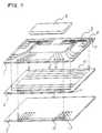
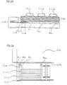
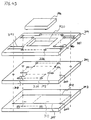
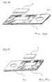
- Fig. 1 is an exploded perspective view which illustrates a multi-layer substrate according to the first embodiment of the present invention in which a semiconductor chip for driving liquid crystal is mounted on the surface of a multi-layer substrate by a face-down bonding method.
- Reference numerals 1, 2 and 3 represent layers of the multi-layer (comprising three layers) substrate composed of a first layer 1, a second layer 2 and a third layer 3.
- a semiconductor chip 4 for driving liquid crystal is mounted on the surface of the first layer 1 in the face-down bonding manner by a known method (for example, a method in which an Au bump of the semiconductor is connected to the substrate by using Ag paste or a method in which an anisotropic conductive film is used or a flip chip method in which soldering bump is used).
- molding members 20 are respectively disposed around the semiconductor chip 4 and between the semiconductor chip 4 and the first layer 1 in order to prevent corrosion and reinforce bonding.
- the molding members 20 are made of sole epoxy, acryl, urethane or polyester material or a mixture or compound of two or more of these materials in the form of a solvent or thermo-hardening or light hardening type or a mixture thereof.
- Input lines 5 corresponding to input pads of the semiconductor chip 4 are formed on the surface of the first layer 1 by patterning.
- the input lines 5 are connected to bus lines 10 of the second layer 2 via through holes 6.
- lands 7 are formed at the leading portions of the input lines 5 for establishing a wire bonding connection with another multi-layer substrate formed similarly and positioned adjacently.
- Output lines 8 corresponding to output pads of the semiconductor chip 4 are formed on the surface of the first layer 1 by patterning. Since the pitch of the terminals of the panel is longer than the pitch of the output pads of the semiconductor chip 4 , the line pattern is widened on the first layer 1 so that the output pads and the terminals of the panel are aligned to one another. Further, through holes 9 are formed at the leading portions of the output lines 8 so that the output lines 8 pass through holes 11 of the second layer 2 and are connected to connection terminals 13 of the panel via through holes 12 of the third layer 3.
- Each of the first, second and the third layers 1, 2 and 3 is made of ceramic substrates manufactured by simultaneously sintering alumina bases at low temperature to have a thickness of 0.25 mm.
- the input lines 5, the output lines 8 and the bus lines 10 are formed by sintering Au, Ag, AgPd or Cu metal paste.
- the through holes 6, 9, 11 and 12 are formed by sintering Au, Ag, AgPd or Cu metal paste.
- the lands 7 and the connection terminals 13 are respectively formed by sintering Au, Ag, AgPd or Cu metal paste.
- the foregoing elements for each layer are formed by a known print patterning method, and the layers are stacked, sintered and integrated so that forming of the multi-layer substrate is completed.
- Each of the metal layers formed by patterning and sintering as described above usually has a thickness of about 0.001 mm to about 0.05 mm. The foregoing thickness may be about 0.05 mm to about 0.2 mm in order to reduce the resistance value.
- the input lines 5, the lands 7, the output lines 8 on the first layer 1 and the connection terminals 13 on the reverse side of the third layer 3 may be formed by photolithographic patterning after the Au, Ag, AgPd or Cu metal paste or a mixture of two or more of these has been printed on the entire surface.
- the thickness of the formed pattern is about 0.001 mm to about 0.2 mm.
- the pattern may be formed by a photolithographic method or a plating method after Au, Ag or Cu has been evaporated or after the thin film has been formed by sputtering. In this case, the thickness of the formed pattern is about 0.0005 mm to about 0.1 mm.
- connection stability can be realized in the portion in which the semiconductor chip 4 and the multi-layer circuit substrate 14 are connected to each other and in the portion in which the connection terminals 13 of the multi-layer circuit substrate 14 and the panel terminals 18 are connected to one another.
- Each of the first, second and the third layers 1, 2 and 3 may be made of different materials, for example, a glass epoxy plate made of a composite material of glass fiber and epoxy resin.
- the thickness of the glass epoxy plate may be about 0.05 mm to about 0.8 mm in place of the employed thickness of 0.1 mm.
- the input lines 5, the output lines 8, the through holes 10, the lands 7 and the connection terminals 13 for each layer are formed by known sub-tractive method or an additive method in which metal, such as copper, is patterned.
- the through holes 6, 9, 11 and 12 are, by a known plating method using metal such as copper, formed for each layer or collectively while stacking the layers.
- the thickness of the patterned metal is about 0.001 mm to about 0.035 mm, it may be about 0.035 mm to about 0.2 mm in order to reduce the resistance and to permit large electric currents to flow.
- the surface of each of the input lines 5, the output lines 8, the bus lines 10, the lands 7, the connection terminals 13, the through holes 6, 9, 11 and 12 may be applied with plating using sole metal, such as Ni, Au, Cr, Co, Pd, Sn, Pb or In or a mixture of two or more of these materials, plating being performed to have a thickness of about 0.00005 mm to about 0.05 mm. If a glass epoxy plate is used, the thickness can be decreased as compared with the foregoing ceramic substrate. Further, the cost can be reduced because ordinary material and manufacturing process can be employed.
- Each of the first, second and the third layers 1, 2 and 3 may be formed by an organic resin film solely made of polyimide (PI), polyethylene terephthalate (PET), polyether sulfon (PES), polycarbonate (PC), polyester (PS), cellulose triacetate (TAC), polysulfon (PS), acryl, epoxy, polyether ether ketone (PEEK) or polyarylate or made of a mixture of two or more of these.
- PI polyimide
- PET polyethylene terephthalate
- PES polyether sulfon
- PC polycarbonate
- PS polyester
- TAC cellulose triacetate
- PS polysulfon
- acryl epoxy
- PEEK polyether ether ketone
- the input lines 5, the output lines 8, the bus lines 10, the lands 7 and the connection terminals 13 for each layer are formed by a known sub-tractive method or an additive method in which metal, such as copper, is patterned.
- the through holes 6, 9, 11 and 12 are formed collectively for each layer or formed after the layers 1, 2 and 3 have been stacked by a known plating method using metal, such as copper.
- a member formed by applying a PI coat (by a known casting method or the like) to metal foil made of, for example, copper, may be patterned and stacked.
- the thickness of the patterned metal is about 0.001 mm to about 0.035 mm, the thickness may be made to be about 0.035 mm to about 0.2 mm in order to reduce the resistance or to permit large electric currents to flow.
- the surface of each of the lines 5, 8, 10, the lands 7, the connection terminals 13, the through holes 6, 9, 11 and 12 may be applied with plating solely using Ni, Au, Cr, Co, Pd, Sn, Pb or In or using a mixture of two or more of these materials.
- the thickness of the layers made by plating is about 0.0001 mm to about 0.05 mm.
- the thickness can be reduced as compared with the thickness realized by using the ceramic substrate or the epoxy glass plate and the connection between the panel terminal 18 and the connection member 19 can easily be established. Therefore, the connection reliability can be improved and the connection process can be simplified.
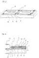
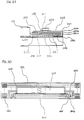
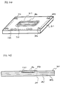
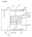
- Fig. 2 illustrates an example in which the multi-layer substrate according to the first embodiment shown in Fig. 1 is connected to a liquid crystal display panel.
- Fig. 3 is an enlarged view which illustrates an essential portion of the connection portion shown in Fig. 2.
- Fig. 4 illustrates the cross sectional view of the essential portion of the connection portion shown in Fig. 2.
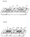
- a light crystal display panel (for example, 640 dots x 480 dots) 16 has 16 multi-layer substrates 14 according to the first embodiment shown in Fig. 1 mounted in direction X and 5 multi-layer substrates 14 in direction Y, the multi-layer substrates 14 thus disposed being connected to the panel terminals 18.
- 12 multi-layer substrates 14 in the direction X and 5 multi-layer substrates 14 in the direction Y are omitted in Fig. 2.
- the terminals 13 of the multi-layer substrate 14 and the panel terminals 18 are connected to one another by the connection member 19.
- the connection member 19 establishes electrical connections and somewhat fixes the multi-layer substrate 14 to the panel.
- the connection member 19 is made of an anisotropic conductive film mainly composed of conductive particles and an adhesive agent.
- the conductive particles are sole soldering particles, sole Ni, Au, Ag, Cu, Pb or Sn particles or a mixture or alloy of two or more of these, complex metal particles made by plating, particles formed by plating sole Ni, Co, Pd, Au, Ag, Cu, Fe, Sn or Pb or a mixture of two or more of these materials on plastic particles (polystyrene, polycarbonate or acryl or the like) or carbon particles.
- the foregoing adhesive agent is a sole styrene butadiene styrene (SBS), epoxy, acryl, polyester or urethane adhesive agent or a mixture or compound of two or more of these materials.
- SBS styrene butadiene styrene
- the anisotropic conductive film is disposed between the panel terminals 18 and the connection terminals 13 of the multi-layer substrate 14. If the anisotropic conductive film is a thermo-hardening film or a blend type of a thermoplastic film and a thermo-hardening film, a heating and pressurizing head is abutted against the multi-layer substrate 14 so that the anisotropic film is hardened and connected.
- the anisotropic conductive film is an ultraviolet hardening type film
- a pressuring head is abutted against the multi-layer substrate 14 and ultraviolet rays are applied to the anisotropic conductive film from a position adjacent to the panel terminal 18 (adjacent to the glass) to harden the ultraviolet hardening type film.
- connection member 19 an anisotropic conductive adhesive agent mainly composed of conductive particles and an adhesive agent is used.
- the conductive particles are sole soldering particles, sole Ni, Au, Ag, Cu, Pb or Sn particles or a mixture or alloy of two or more of these materials, complex metal particles made by plating, particles formed by plating sole Ni, Co, Pd, Au, Ag, Cu, Fe, Sn or Pb or a mixture of two or more of these materials on plastic particles (polystyrene, polycarbonate or acryl or the like) or carbon particles.
- the foregoing adhesive agent is a sole styrene butadiene styrene (SBS), epoxy, acryl, polyester or urethane adhesive agent or a mixture or compound of two or more of these materials.
- the anisotropic conductive adhesive agent is a fluid or paste agent and applied to the portion in which the panel terminal 16 is connected by a known method, for example, printing or a dispensing method using a dispenser. If the anisotropic conductive adhesive agent is a thermo-hardening agent or a blended agent of a thermoplastic agent and a thermo-hardening agent, a heating and pressuring head is abutted against the multi-layer substrate 14 so that the agent is hardened and connected.
- the anisotropic conductive film is an ultraviolet hardening type film
- a pressuring head is abutted against the multi-layer substrate 14 and ultraviolet rays are applied to the anisotropic conductive film from a position adjacent to the panel terminal 18 (adjacent to the glass) to harden the ultraviolet hardening type film.
- the molding 21 In order to protect the exposed portion of the panel terminal 18, a molding 21 is placed.
- the molding 21 also serves to fix the multi-layer substrate 14 to the panel.
- the molding 21 is made of sole epoxy, acryl, urethane or polyester material or a mixture or compound of two or more of these materials of any one of solvent type, thermo-hardening type, or light hardening type or a mixture thereof.
- the bus lines between adjacent multi-layer substrates 14 are connected by wire bonding with wires 15 via the lands 7.
- the wires 15 may be made of metal such as Au, Al or Cu or the like or their alloy (alloy containing Be, Si or Mg or the like included).
- the width of the wire-bonded portion is so determined as to be narrower than the width of the multi-layer substrate, resulting in that the wire-bonded portion can be mounted in a satisfactorily compact manner in which it is included within the outline of the panel 16.
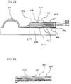
- the connection member 19 may be an anisotropic conductive film arranged as shown in Fig. 21 and mainly composed of conductive particles 32 and an adhesive agent 33.
- the thickness (h) of the adhesive agent 33 is made thinner than the particle size (d) of the conductive particles 32.
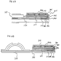
- the anisotropic conductive film 31 may be formed on a separator 34 (a teflon or a PET sheet (film) or a paper sheet).
- the conductive particles 32 are, as shown in Fig.
- sole soldering particles Ni, Au, Ag, Cu, Pb or Sn particles or a mixture or alloy of two or more of these, complex metal particles made by plating, particles formed by plating sole Ni, Au, Cu or Fe or a mixture of two or more of these materials on plastic particles (polystyrene, polycarbonate or acryl or the like) or carbon particles.
- the particle size (d) is about 0.001 mm to about 0.020 mm.
- the adhesive agent 27 is sole styrene butadiene styrene (SBS), epoxy, acrylic, polyester or urethane adhesive agent or a mixture or compound of two or more of these materials having a thickness (h) ranging from about 0.0005 mm to about 0.018 mm.
- the anisotropic conductive film 31 is disposed between the panel terminal 18 and the connection terminal 13 of the multi-layer substrate 14. If the anisotropic conductive film 31 is a thermo-hardening agent or a blend type of a thermoplastic agent and a thermo-hardening agent, a heating and pressurizing head is abutted against the multi-layer substrate 14 so that the anisotropic adhesive agent is hardened and connected. If the anisotropic conductive film 31 is an ultraviolet hardening type adhesive agent, a pressuring head is abutted against the multi-layer substrate 14 and ultraviolet rays are applied to the anisotropic conductive adhesive agent from a position adjacent to the panel terminal 18 (adjacent to the glass) to harden and connect the ultraviolet hardening type film.
- the adhesive agent 33 can be removed satisfactorily at the time of applying pressure so that the panel terminal 18 and the connection terminal 13 of the multi-layer substrate 14 can be assuredly electrically connected to each other by the conductive particles 32 (see Fig. 10).
- the thus established connection state is maintained by the adhesive agent 33 so that satisfactory connection reliability is maintained.
- FIG. 23 Another conductive member may be employed as shown in Fig. 23 which has an arrangement that an anisotropic adhesive agent 35 in the form of fluid or paste including the conductive particles 32 and the adhesive agent 33 is applied to the portion, in which the panel terminal 16 is connected, by a known method, such as a printing method or a dispensing method using a dispenser.
- a known method such as a printing method or a dispensing method using a dispenser.
- the viscosity and the thixotropic characteristics of the anisotropic conductive agent 35 are so controlled as to make the thickness (h) of the adhesive agent 33 to be smaller than the particle size (d) of the conductive particles 32.
- the connection can reliably be established as shown in Fig. 24 by a method similar to that for connecting the foregoing anisotropic conductive film with pressure.
- a molding 21 is placed.
- the molding 21 also serves to fix the multi-layer substrate 14 to the panel.
- the molding 21 is made of sole epoxy, acryl, urethane or polyester material or a mixture or compound of two or more of these materials of any one of solvent type, thermo-hardening type, or light hardening type or a mixture thereof.
- the bus lines between adjacent multi-layer substrates 14 are connected by wire bonding with wires 15 via the lands 7.
- the wires 15 may be made of metal such as Au, Al or Cu or the like or their alloy (alloy containing Be, Si or Mg or the like included).
- the width of the wire-bonded portion is so determined as to be narrower than the width of the multi-layer substrate, resulting in that the wire-bonded portion can be mounted in a satisfactorily compact manner in which it is included within the outline of the panel 16 as shown in Fig. 4.
- use of the multi-layer substrate according to this embodiment enables the lines to be wired in the cross manner in the same multi-layer substrate as contrasted with the conventional TAB method using individual bus substrates to wire the bus lines in the cross manner. Therefore, the overall size can be reduced as compared with the TAB method by raising the density of the lines wired on the substrate. Further, the cost can be reduced because individual bus lines are not used.
- the conventional COG method has the arrangement that the cross wiring of the bus lines is performed on the panel substrate, a wide area is required to wire the bus lines. Further, metal lines must be used to reduce the resistance value of the wired lines, resulting in an enlargement of the cost.
- use of the multi-layer substrate according to this embodiment enables the space required to wire the bus lines and the cost to be reduced as compared with the COG method.
- Fig. 5 is an exploded perspective view which illustrates a multi-layer substrate of a liquid crystal display apparatus according to a second embodiment of the present invention in which a semiconductor chip for driving liquid crystal is mounted on the surface of a multi-layer substrate by wire bonding.
- Wire bonding lands 22 are, on the surface of the first layer 1 of the multi-layer substrate, formed for the input lines 5 and the output lines 8 to correspond to the input/output pads of the semiconductor chip 4 .
- the residual factors, such as the pattern, through holes, the method of forming the multi-layer substrate, the arrangement and the structure are the same as those according to the first embodiment.
- the reverse side of the semiconductor chip 4 is secured to the surface of the multi-layer substrate. Further, the input/output pads of the semiconductor chip 4 and the lands 22 on the surface of the first layer 1 of the multi-layer substrate are wire-bonded to one another. Wire 23 for use to connect the multi-layer substrates according to the first embodiment may be used here. Further, the bonded portions and the wired portions are, although omitted from illustration, applied with molding material to be protected and reinforced similarly to the first embodiment.
- bus lines between the adjacent multi-layer substrates are connected by wire bonding similarly to the first embodiment.
- the bonded portions and the wired portions are, although omitted from illustration, applied with molding material to be protected and reinforced similarly to the first embodiment.
- use of the multi-layer substrate according to this embodiment enables the size and the cost to be reduced similarly to the first embodiment as compared with the conventional TAB method and the COG method.
- Fig. 6 illustrates a liquid crystal display apparatus according to the present invention in which the multi-layer substrates 14 having the face-down-bonded semiconductor chips 4 thereon is connected to the panel terminal 18 of the liquid crystal display panel by using the anisotropic conductive film 19 similarly to the first embodiment.
- the essential portion of the connection portion is arranged to be similar to that according to the first embodiment shown in Fig. 4.
- the leading portions of the input lines of the first layer 1 of the multi-layer substrate are formed into shapes adaptable to be connected to heat seal or flexible substrates in place of the wire bonding lands.
- connection substrate 24 may be a heat seal or a flexible substrate.
- the width of the portion, in which the connection substrate 24 is connected, is so determined as to be narrower than the width of the multi-layer substrate 14, resulting in that the wire-bonded portion can be mounted in a satisfactorily compact manner in which it is included within the outline of the panel 16 as shown in Fig. 4.
- use of the multi-layer substrate according to this embodiment enables the size and the cost to be reduced similarly to the first embodiment as compared with the conventional TAB method and the COG method.
- connection of the semiconductor chip for driving liquid crystal to the surface of the multi-layer substrate and the electrical connection between the adjacent multi-layer substrates may be established by combining the methods according to first, second and the third embodiments. In any case, the size and the cost can be reduced similarly.
- the multi-layer substrate having the semiconductor chip for use in the foregoing embodiments mounted thereon can be mounted on another display apparatus or an electronic printing apparatus such that it can be mounted on a plasma display or an EL display apparatus by changing the foregoing semiconductor chip to a semiconductor chip for driving the plasma display or a semiconductor chip for driving the EL.
- a semiconductor chip for driving a thermal head By similarly mounting a semiconductor chip for driving a thermal head on the multi-layer substrate and by similarly connecting the multi-layer substrate to the thermal head, application to an electronic printing apparatus can be realized.
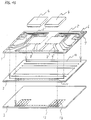
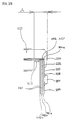
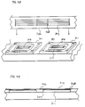
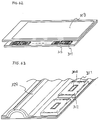
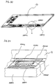
- Fig. 7 is an exploded perspective view which illustrates a liquid crystal display apparatus according to the present invention in which a multi-layer substrate according to this embodiment includes a semiconductor chip for driving liquid crystal face-down bonded thereon.
- Reference numerals 1, 2 and 3 represent layers of the multi-layer (comprising three layers) substrate composed of a first layer 1, a second layer 2 and a third layer 3.
- a semiconductor chip 4 for driving liquid crystal is mounted on the surface of the first layer 1 in the face-down bonding manner by a known method (for example, a method in which an Au bump of the semiconductor is connected to the substrate by using Ag paste or a method in which an anisotropic conductive film is used or a flip chip method in which soldering is performed).
- molding members 20 are respectively disposed around the semiconductor chip 4 and between the semiconductor chip 4 and the first layer 1 in order to prevent corrosion and reinforce bonding.
- the molding members 20 are made of sole epoxy, acryl, urethane or polyester material or a mixture or compound of two or more of these materials in the form of a solvent or thermo-hardening or light hardening type or a mixture thereof.
- Input lines 5 corresponding to input pads of the semiconductor chip 4 are formed on the surface of the first layer 1 by patterning.
- the input lines 5 are connected to bus lines 10 of the second layer 2 via through holes 6 and through holes 25.
- the input lines 5 are connected to the connection terminals 27 formed on the reverse side of the third layer 3 via the through holes 26 formed in the third layer 3.
- the connection terminals 27 are respectively formed into a proper shape to have a proper size and a thickness to be connected to the connection terminals 29 of the bus lines 28 on the panel.
- connection terminals 27 are disposed on the side of the multi-layer substrate 14 perpendicular to the side on which the connection terminals 13 for establishing the connection with the panel are disposed. Although the illustrated structure comprises the connection terminals 27 disposed in a line, a two-line configuration may be employed.
- Output lines 8 corresponding to output pads of the semiconductor chip 4 are formed on the surface of the first layer 1 by patterning. Since the pitch of the terminals of the panel is longer than the pitch of the output pads of the semiconductor chip 4 , the line pattern is widened on the first layer 1 so that the output pads and the terminals of the panel are aligned to one another. Further, through holes 9 are formed at the leading portions of the output lines 8 so that the output lines 8 pass through the through holes 11 of the second layer 2 and are connected to connection terminals 13 of the panel via through holes 12 of the third layer 3.
- the coincidence may be made over a plurality of layers (two or more layers) in place of making only one layer coincide.
- Each of the first, second and the third layers 1, 2 and 3 is made of ceramic substrates manufactured by simultaneously sintering alumina bases at low temperature to have a thickness of 0.25 mm.
- the input lines 5, the output lines 8 and the bus lines 10 are formed by sintering solely or mixture of Au, Ag, AgPd or Cu metal paste.
- the through holes 6, 9, 11, 12, 25 and 26 are formed by sintering Au, Ag, AgPd or Cu metal paste.
- connection terminals 13 and 27 are respectively formed by sintering solely Au, Ag, AgPd or Cu metal paste or a mixture of two or more of these.
- each layer is formed by a known print patterning method, and the layers are stacked sintered and integrated so that forming of the multi-layer substrate is completed.
- Each of the metal layers formed by patterning and sintering as described above usually has a thickness of about 0.001 mm to about 0.05 mm.
- the foregoing thickness may be about 0.05 mm to about 0.2 mm in order to reduce the resistance value.
- the input lines 5 and the output lines 8 on the surface of the first layer 1 and the connection terminals 13 and 27 on the third layer 3 may be formed by photolithographic patterning after the Au, Ag, AgPd or Cu metal paste or a mixture paste of two or more of these materials has been printed on the entire surface.
- the thickness of the formed pattern is about 0.001 mm to about 0.2 mm.
- the pattern may be formed by a photolithographic method or a plating method after Au, Ag or Cu has been evaporated or after the thin film has been formed by sputtering. In this case, the thickness of the formed pattern is about 0.0005 mm to about 0.1 mm.
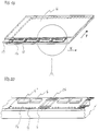
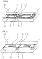
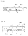
- Fig. 8 is an exploded view which illustrates an essential portion in which the multi-layer substrate according to this embodiment shown in Fig. 7 is connected to the liquid crystal display panel.
- the cross section (section x-x of Fig. 8) of the essential portion of the connection portion is as shown in Fig. 4 similarly to the first embodiment.
- Connection terminals 18, bus lines 28 and connection terminals 29 to be disposed at the end portions of the bus lines 28 are, by patterning, formed on the panel 16 to correspond to the portion in which the multi-layer substrate 14 will be mounted. Although a straight-line pattern is formed in the structure shown in Fig. 8, the pattern may be formed fully in an allowable area in terms of wiring if the resistance of the circuit and that of the connections are intended to be reduced.
- the bus lines 28 on the panel serve as bus lines for establishing the connections between the foregoing multi-layer substrates.
- Fig. 9 illustrates a structure arranged substantially similarly to that according to the embodiment shown in Fig. 8 except for an arrangement in which the connection terminals 13 of the multi-layer substrate 14 are disposed inside the panel 16.
- the cross section (section y-y of Fig. 9) of the essential portion of the connection portion is as shown in Fig. 10 whereby the length of each of lines arranged from the panel terminals 18 to the inside portion of the panel can be shorter than that according to the embodiment shown in Fig. 4. As a result, an effect can be obtained in that the circuit resistance can be reduced.
- connection terminals 13, the panel terminals 18, the connection terminals 27 and the panel terminals 28 are connected to one another by connection members 19.
- the connection members 19 maintain the electrical connections and also act to fix somewhat the multi-layer substrates 14 to the panel.
- the connection member 19 is made of an anisotropic conductive film mainly composed of conductive particles and an adhesive agent.
- the conductive particles are sole soldering particles, sole Ni, Au, Ag, Cu, Pb or Sn particles or a mixture or alloy of two or more of these, complex metal particles made by plating, particles formed by plating sole Ni, Co, Pd, Au, Ag, Cu, Fe, Sn or Pb or a mixture of two or more of these materials on plastic particles (polystyrene, polycarbonate or acryl or the like) or carbon particles.
- the foregoing adhesive agent is a sole styrene butadiene styrene (SBS), epoxy, acryl, polyester or urethane adhesive agent or a mixture or compound of two or more of these materials.
- SBS styrene butadiene styrene
- the anisotropic conductive film is disposed between the panel terminals 18 and the connection terminals 13 and 27 of the multi-layer substrate 14. If the anisotropic conductive film is a thermo-hardening film or a blend type of a thermoplastic film and a thermo-hardening film, a heating and pressurizing head is abutted against the multi-layer substrate 14 so that the anisotropic film is hardened and connected.
- the anisotropic conductive film is an ultraviolet hardening type film
- a pressuring head is abutted against the multi-layer substrate 14 and ultraviolet rays are applied to the anisotropic conductive film from a position adjacent to the panel terminals 18 and 29 (adjacent to the glass) to harden the ultraviolet hardening type film.
- the pressuring head is formed into a U-shape facing sidewards or if a multiplicity of the pressuring heads are used to correspond to the configuration of the connection terminals 13 and 27, the input/output terminals of the multi-layer substrate 14 can be collectively connected to the corresponding panel terminals 18 and 29 while necessitating only one pressurizing process.
- an anisotropic conductive adhesive agent which is mainly composed of conductive particles and an adhesive agent.
- the conductive particles are sole soldering particles, sole Ni, Au, Ag, Cu, Pb or Sn particles or a mixture or alloy of two or more of these materials, complex metal particles made by plating, particles formed by plating sole Ni, Co, Pd, Au, Ag, Cu, Fe, Sn or Pb or a mixture of two or more of these materials on plastic particles (polystyrene, polycarbonate or acryl or the like) or carbon particles.
- the foregoing adhesive agent is a sole styrene butadiene styrene (SBS), epoxy, acryl, polyester or urethane adhesive agent or a mixture or compound of two or more of these materials.
- the anisotropic conductive adhesive agent is a fluid or paste agent and applied to the portion in which the panel terminal 16 is connected by a known method, for example, printing or a dispensing method using a dispenser. If the anisotropic conductive adhesive agent is a thermo-hardening agent or a blended agent of a thermoplastic agent and a thermo-hardening agent, a heating and pressuring head is abutted against the multi-layer substrate 14 so that the agent is hardened and connected.
- the anisotropic conductive adhesive agent is an ultraviolet hardening type adhesive agent
- a pressuring head is abutted against the multi-layer substrate 14 and ultraviolet rays are applied to the anisotropic conductive film from a position adjacent to the panel terminals 18 and 19 (adjacent to the glass) to harden the ultraviolet hardening type film.
- the pressuring head is formed into a U-shape facing sidewards or if a multiplicity of the pressuring heads are used to correspond to the configuration of the connection terminals 13 and 27, the input/output terminals of the multi-layer substrate 14 can be collectively connected to the corresponding panel terminals 18 and 29 while necessitating only one pressurizing process.
- a molding 21 is placed.
- the molding 21 also serves to fix the multi-layer substrate 14 to the panel.
- the molding 21 is made of sole epoxy, acryl, urethane or polyester material or a mixture or compound of two or more of these materials of any one of solvent type, thermo-hardening type, or light hardening type or a mixture thereof.
- the multi-layer substrate can be mounted in a compact manner within the outline of the panel 16.
- the bus lines formed on the panel to serves as the means for establishing the electrical connections between the multi-layer substrates enables the bus lines to be formed simultaneously with the other lines on the panel. Therefore, an individual forming process does not need to be performed. Further, individual elements such as the heat seal can be omitted. In addition, the fact that the connections of the input and output terminals can be collectively established causes the manufacturing process to be simplified.
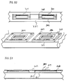
- Fig. 11 is an exploded perspective view which illustrates a liquid crystal display apparatus according to the present invention in which a multi-layer substrate according to this embodiment includes a semiconductor chip for driving liquid crystal face-down bonded thereon.
- Reference numerals 1, 2 and 3 represent layers of the multi-layer (comprising three layers) substrate composed of a first layer 1, a second layer 2 and a third layer 3.
- a semiconductor chip 4 for driving liquid crystal is mounted on the surface of the first layer 1 in the face-down bonding manner by a known method (for example, a method in which an Au bump of the semiconductor is connected to the substrate by using Ag paste or a method in which an anisotropic conductive film is used or a flip chip method in which soldering is performed).
- molding members 20 are respectively disposed around the semiconductor chip 4 and between the semiconductor chip 4 and the first layer 1 in order to prevent corrosion and reinforce bonding.
- the molding members 20 are made of sole epoxy, acryl, urethane or polyester material or a mixture or compound of two or more of these materials in the form of a solvent or thermo-hardening or light hardening type or a mixture thereof.
- Input lines 5 corresponding to input pads of the semiconductor chip 4 are formed on the surface of the first layer 1 by patterning.
- the input lines 5 are connected to bus lines 10 of the second layer 2 via through holes 6 and through holes 25.
- the bus lines 10 are connected to through holes 30 of the second layer 2 and connected to the connection terminals 27 formed on the reverse side of the third layer 3 via the through holes 30 and the through holes 26 of the second layer 2.
- the connection terminals 27 are disposed to substantially run parallel to the connection terminals 13.
- connection terminals 27 and the connection terminals 13 are formed into the same shape, have the same size and thickness.
- Fig. 11 illustrates the structure in which the connection terminals 13 and 27 respectively have the same shape and are disposed at the same pitch, the connection terminals 13 and 27 may be respectively different from one another.
- the through holes 13 and 26 are disposed in one line, they may be disposed to form plural lines.
- Output lines 8 corresponding to output pads of the semiconductor chip 4 are formed on the surface of the first layer 1 by patterning. Since the pitch of the terminals of the panel is longer than the pitch of the output pads of the semiconductor chip 4 , the line pattern is widened on the first layer 1 so that the output pads and the terminals of the panel are aligned to one another. Further, through holes 9 are formed at the leading portions of the output lines 8 so that the output lines 8 pass through the through holes 11 of the second layer 2 and and connected to connection terminals 13 of the panel via through holes 12 of the third layer 3.
- the coincidence may be made over a plurality of layers (two or more layers) in place of making only one layer coincide.
- Each of the first, second and the third layers 1, 2 and 3 is made of ceramic substrates manufactured by simultaneously sintering alumina bases at low temperature to have a thickness of 0.25 mm.
- the input lines 5, the output lines 8 and the bus lines 10 are formed by sintering solely or mixture of Au, Ag, AgPd or Cu metal paste.
- the through holes 6, 9, 11, 12, 25, 26 and 30 are formed by sintering Au, Ag, AgPd or Cu metal paste.
- connection terminals 13 and 27 are respectively formed by sintering solely Au, Ag, AgPd or Cu metal paste or a mixture of two or more of these.
- each layer is formed by a known print patterning method, and the layers are stacked sintered and integrated so that forming of the multi-layer substrate is completed.
- Each of the metal layers formed by patterning and sintering as described above usually has a thickness of about 0.001 mm to about 0.05 mm.
- the foregoing thickness may be about 0.05 mm to about 0.2 mm in order to reduce the resistance value.
- the input lines 5 and the output lines 8 on the surface of the first layer 1 and the connection terminals 13 and 27 on the third layer 3 may be formed by photolithographic patterning after the Au, Ag, AgPd or Cu metal paste or a mixture paste of two or more of these materials has been printed on the entire surface.
- the thickness of the formed pattern is about 0.001 mm to about 0.2 mm.
- the pattern may be formed by a photolithographic method or a plating method after Au, Ag or Cu has been evaporated or after the thin film has been formed by sputtering. In this case, the thickness of the formed pattern is about 0.0005 mm to about 0.1 mm.
- Fig. 12 is an exploded view which illustrates an essential portion in which the multi-layer substrate according to this embodiment shown in Fig. 7 is connected to the liquid crystal display panel.
- the cross section (section x-x of Fig. 12) of the essential portion of the connection portion is as shown in Fig. 4 similarly to the first embodiment.
- Connection terminals 18, bus lines 28 and connection terminals 29 to be disposed at the end portions of the bus lines 28 are, by patterning, formed on the panel 16 to correspond to the portion in which the multi-layer substrate 14 will be mounted.
- the connection terminals 18 and 29 are disposed on one straight line.
- the bus lines 28 are simply illustrated by a continuous line in Fig.
- bus lines 28 on the panel serve as bus lines for establishing the connections between the foregoing multi-layer substrates.
- connection terminals 13, the panel terminals 18, the connection terminals 27 and the panel terminals 28 of the multi-layer substrate 14 are connected to one another by connection members 19.
- the connection members 19 maintain the electrical connections and also act to fix somewhat the multi-layer substrates 14 to the panel.
- the connection member 19 is made of an anisotropic conductive film mainly composed of conductive particles and an adhesive agent.
- the conductive particles are sole soldering particles, sole Ni, Au, Ag, Cu, Pb or Sn particles or a mixture or alloy of two or more of these, complex metal particles made by plating, particles formed by plating sole Ni, Co, Pd, Au, Ag, Cu, Fe, Sn or Pb or a mixture of two or more of these materials on plastic particles (polystyrene, polycarbonate or acryl or the like) or carbon particles.
- the foregoing adhesive agent is a sole styrene butadiene styrene (SBS), epoxy, acryl, polyester or urethane adhesive agent or a mixture or compound of two or more of these materials.
- SBS styrene butadiene styrene
- the anisotropic conductive film is disposed between the panel terminals 18 and the connection terminals 13 and 27 of the multi-layer substrate 14. If the anisotropic conductive film is a thermo-hardening film or a blend type of a thermoplastic film and a thermo-hardening film, a heating and pressurizing head is abutted against the multi-layer substrate 14 so that the anisotropic film is hardened and connected.
- the anisotropic conductive film is an ultraviolet hardening type film
- a pressuring head is abutted against the multi-layer substrate 14 and ultraviolet rays are applied to the anisotropic conductive film from a position adjacent to the panel terminals 18 and 29 (adjacent to the glass) to harden the ultraviolet hardening type film. Since the connection terminals 13 and 27 are disposed on one straight line, the pressurizing head may be formed into a simple straight shape so that the connections can be established by using a simple pressurizing and connecting device. Further, the input/output terminals of the multi-layer substrate 14 can be collectively connected to the corresponding panel terminals 18 and 29 while necessitating only one pressurizing process.
- an anisotropic conductive adhesive agent which is mainly composed of conductive particles and an adhesive agent.
- the conductive particles are sole soldering particles, sole Ni, Au, Ag, Cu, Pb or Sn particles or a mixture or alloy of two or more of these, complex metal particles made by plating, particles formed by plating sole Ni, Co, Pd, Au, Ag, Cu, Fe, Sn or Pb or a mixture of two or more of these materilas on plastic particles (polystyrene, polycarbonate or acryl or the like) or carbon particles.
- the foregoing adhesive agent is a sole styrene butadiene styrene (SBS), epoxy, acryl, polyester or urethane adhesive agent or a mixture or compound of two or more of these materials.
- the anisotropic conductive adhesive agent is a fluid or paste agent and applied to the portion in which the panel terminal 16 is connected by a known method, for example, printing or a dispensing method using a dispenser. If the anisotropic conductive adhesive agent is a thermo-hardening agent or a blended agent of a thermoplastic agent and a thermo-hardening agent, a heating and pressuring head is abutted against the multi-layer substrate 14 so that the agent is hardened and connected.
- the anisotropic conductive adhesive agent is an ultraviolet hardening type adhesive agent
- a pressuring head is abutted against the multi-layer substrate 14 and ultraviolet rays are applied to the anisotropic conductive film from a position adjacent to the panel terminals 18 and 19 (adjacent to the glass) to harden the ultraviolet hardening type film. Since the connection terminals 13 and 27 are disposed on one straight line, the pressurizing head may be formed into a simple straight shape so that the connections can be established by using a simple pressurizing and connecting device. Further, the input/output terminals of the multi-layer substrate 14 can be collectively connected to the corresponding panel terminals 18 and 29 while necessitating only one pressurizing process.
- a molding 21 is placed.
- the molding 21 also serves to fix the multi-layer substrate 14 to the panel.
- the molding 21 is made of sole epoxy, acryl, urethane or polyester material or a mixture or compound of two or more of these materials of any one of solvent type, thermo-hardening type, or light hardening type or a mixture thereof.
- the multi-layer substrate can be mounted in a compact manner within the outline of the panel 16.
- the bus lines formed on the panel to serves as the means for establishing the electrical connections between the multi-layer substrates enables the bus lines to be formed simultaneously with the other lines on the panel. Therefore, an individual forming process does not need to be performed. Further, individual elements such as the heat seal can be omitted. In addition, the fact that the connections of the input and output terminals can be collectively established causes the manufacturing process to be simplified.
- Fig. 13 illustrates a structure arranged substantially similarly to that according to the embodiment shown in Fig. 12 except for an arrangement in which the connection terminals 13 of the multi-layer substrate 14 are disposed inside the panel 16.
- the cross section (section Y-Y of Fig. 13) of the essential portion of the connection portion is as shown in Fig. 10 whereby the length of each of lines arranged from the panel terminals 18 to the inside portion of the panel can be shorter than that according to the embodiment shown in Fig. 4. As a result, an effect can be obtained in that the circuit resistance can be reduced.
- connection terminals 13, the panel terminals 18, the connection terminals 27 and the panel terminals 28 of the multi-layer substrate 14 are connected to one another by connection members 19.
- the connection members 19 maintain the electrical connections and also act to fix somewhat the multi-layer substrates 14 to the panel.
- the connection member 19 is made of an anisotropic conductive film mainly composed of conductive particles and an adhesive agent.
- the conductive particles are sole soldering particles, sole Ni, Au, Ag, Cu, Pb or Sn particles or a mixture or alloy of two or more of these, complex metal particles made by plating, particles formed by plating sole Ni, Co, Pd, Au, Ag, Cu, Fe, Sn or Pb or a mixture of two or more of these materials on plastic particles (polystyrene, polycarbonate or acryl or the like) or carbon particles.
- the foregoing adhesive agent is a sole styrene butadiene styrene (SBS), epoxy, acryl, polyester or urethane adhesive agent or a mixture or compound of two or more of these materials.
- SBS styrene butadiene styrene
- the anisotropic conductive film is disposed between the panel terminals 18 and the connection terminals 13 and 27 of the multi-layer substrate 14. If the anisotropic conductive film is a thermo-hardening film or a blend type of a thermoplastic film and a thermo-hardening film, a heating and pressurizing head is abutted against the multi-layer substrate 14 so that the anisotropic film is hardened and connected.
- the anisotropic conductive film is an ultraviolet hardening type film
- a pressuring head is abutted against the multi-layer substrate 14 and ultraviolet rays are applied to the anisotropic conductive film from a position adjacent to the panel terminals 18 and 29 (adjacent to the glass) to harden the ultraviolet hardening type film. Since the connection terminals 13 and 27 are disposed on one straight line, the pressurizing head may be formed into a simple straight shape so that the connections can be established by using a simple pressurizing and connecting device. Further, the input/output terminals of the multi-layer substrate 14 can be collectively connected to the corresponding panel terminals 18 and 29 while necessitating only one pressurizing process.
- an anisotropic conductive adhesive agent which is mainly composed of conductive particles and an adhesive agent.
- the conductive particles are sole soldering particles, sole Ni, Au, Ag, Cu, Pb or Sn particles or a mixture or alloy of two or more of these, complex metal particles made by plating, particles formed by plating sole Ni, Co, Pd, Au, Ag, Cu, Fe, Sn or Pb or a mixture of two or more of these materials on plastic particles (polystyrene, polycarbonate or acryl or the like) or carbon particles.
- the foregoing adhesive agent is a sole styrene butadiene styrene (SBS), epoxy, acryl, polyester or urethane adhesive agent or a mixture or compound of two or more of these materials.
- the anisotropic conductive adhesive agent is a fluid or paste agent and applied to the portion in which the panel terminal 16 is connected by a known method, for example, printing or a dispensing method using a dispenser. If the anisotropic conductive adhesive agent is a thermo-hardening agent or a blended agent of a thermoplastic agent and a thermo-hardening agent, a heating and pressuring head is abutted against the multi-layer substrate 14 so that the agent is hardened and connected.
- the anisotropic conductive adhesive agent is an ultraviolet hardening type adhesive agent
- a pressuring head is abutted against the multi-layer substrate 14 and ultraviolet rays are applied to the anisotropic conductive film from a position adjacent to the panel terminals 18 and 19 (adjacent to the glass) to harden the ultraviolet hardening type film. Since the connection terminals 13 and 27 are disposed on one straight line, the pressurizing head may be formed into a simple straight shape so that the connections can be established by using a simple pressurizing and connecting device. Further, the input/output terminals of the multi-layer substrate 14 can be collectively connected to the corresponding panel terminals 18 and 29 while necessitating only one pressurizing process.
- a molding 21 is placed.
- the molding 21 also serves to fix the multi-layer substrate 14 to the panel.
- the molding 21 is made of sole epoxy, acryl, urethane or polyester material or a mixture or compound of two or more of these materilas of any one of solvent type, thermo-hardening type, or light hardening type or a mixture thereof.
- the multi-layer substrate can be mounted in a compact manner within the outline of the panel 16.
- the bus lines formed on the panel to serves as the means for establishing the electrical connections between the multi-layer substrates enables the bus lines to be formed simultaneously with the other lines on the panel. Therefore, an individual forming process does not need to be performed. Further, individual elements such as the heat seal can be omitted. In addition, the fact that the connections of the input and output terminals can be collectively established causes the manufacturing process to be simplified.
- Fig. 14 illustrates a structure arranged similarly to that according to the embodiment shown in Fig. 12 except for an arrangement that the bus lines 28 on the panel are also disposed in an area in the panel that does not affect the display n addition to the area on which the multi-layer substrate 13 will be mounted. Therefore, the area that can be used to form the bus lines 28 can be widened, the width of the bus lines can be enlarged to reduce the circuit resistance while eliminating a necessity of enlarging the area required to mount the multi-layer substrates 14. The reduction in the resistance value of the bus lines enables an effect to be obtained in that the quality of display made by the liquid crystal display apparatus can be improved.
- the cross section (section Z-Z of Fig. 14) of the essential portion of the connection portion is as shown in Fig. 10. As shown in the drawing, a liquid crystal display apparatus can be provided in which the area required to mount the multi-layer substrate 14 can further be reduced and which exhibits excellent quality of display.
- connection terminals 13, the panel terminals 18, the connection terminals 27 and the panel terminals 28 of the multi-layer substrate 14 are connected to one another by connection members 19.
- the connection members 19 maintain the electrical connections and also act to fix somewhat the multi-layer substrates 14 to the panel.
- the connection member 19 is made of an anisotropic conductive film mainly composed of conductive particles and an adhesive agent.
- the conductive particles are sole soldering particles, sole Ni, Au, Ag, Cu, Pb or Sn particles or a mixture or alloy of two or more of these, complex metal particles made by plating, particles formed by plating sole Ni, Co, Pd, Au, Ag, Cu, Fe, Sn or Pb or a mixture of two or more of these materials on plastic particles (polystyrene, polycarbonate or acryl or the like) or carbon particles.
- the foregoing adhesive agent is a sole styrene butadiene styrene (SBS), epoxy, acryl, polyester or urethane adhesive agent or a mixture or compound of two or more of these materials.
- SBS styrene butadiene styrene
- the anisotropic conductive film is disposed between the panel terminals 18 and the connection terminals 13 and 27 of the multi-layer substrate 14. If the anisotropic conductive film is a thermo-hardening film or a blend type of a thermoplastic film and a thermo-hardening film, a heating and pressurizing head is abutted against the multi-layer substrate 14 so that the anisotropic film is hardened and connected.
- the anisotropic conductive film is an ultraviolet hardening type film
- a pressuring head is abutted against the multi-layer substrate 14 and ultraviolet rays are applied to the anisotropic conductive film from a position adjacent to the panel terminals 18 and 29 (adjacent to the glass) to harden the ultraviolet hardening type film. Since the connection terminals 13 and 27 are disposed on one straight line, the pressurizing head may be formed into a simple straight shape so that the connections can be established by using a simple pressurizing and connecting device. Further, the input/output terminals of the multi-layer substrate 14 can be collectively connected to the corresponding panel terminals 18 and 29 while necessitating only one pressurizing process.
- an anisotropic conductive adhesive agent which is mainly composed of conductive particles and an adhesive agent.
- the conductive particles are sole soldering particles, sole Ni, Au, Ag, Cu, Pb or Sn particles or a mixture or alloy of two or more of these, complex metal particles made by plating, particles formed by plating sole Ni, Co, Pd, Au, Ag, Cu, Fe, Sn or Pb or a mixture of two or more of these materials on plastic particles (polystyrene, polycarbonate or acryl or the like) or carbon particles.
- the foregoing adhesive agent is a sole styrene butadiene styrene (SBS), epoxy, acryl, polyester or urethane adhesive agent or a mixture or compound of two or more of these materials.
- the anisotropic conductive adhesive agent is a fluid or paste agent and applied to the portion in which the panel terminal 16 is connected by a known method, for example, printing or a dispensing method using a dispenser. If the anisotropic conductive adhesive agent is a thermo-hardening agent or a blended agent of a thermoplastic agent and a thermo-hardening agent, a heating and pressuring head is abutted against the multi-layer substrate 14 so that the agent is hardened and connected.
- the anisotropic conductive adhesive agent is an ultraviolet hardening type adhesive agent
- a pressuring head is abutted against the multi-layer substrate 14 and ultraviolet rays are applied to the anisotropic conductive film from a position adjacent to the panel terminals 18 and 19 (adjacent to the glass) to harden the ultraviolet hardening type film. Since the connection terminals 13 and 27 are disposed on one straight line, the pressurizing head may be formed into a simple straight shape so that the connections can be established by using a simple pressurizing and connecting device. Further, the input/output terminals of the multi-layer substrate 14 can be collectively connected to the corresponding panel terminals 18 and 29 while necessitating only one pressurizing process.
- a molding 21 is placed.
- the molding 21 also serves to fix the multi-layer substrate 14 to the panel.
- the molding 21 is made of sole epoxy, acryl, urethane or polyester material or a mixture or compound of two or more of these materials of any one of solvent type, thermo-hardening type, or light hardening type or a mixture thereof.
- the multi-layer substrate can be mounted in a compact manner within the outline of the panel 16.
- the bus lines formed on the panel to serves as the means for establishing the electrical connections between the multi-layer substrates enables the bus lines to be formed simultaneously with the other lines on the panel. Therefore, an individual forming process does not need to be performed. Further, individual elements such as the heat seal can be omitted.
- the fact that the connections of the input and output terminals can be collectively established causes the manufacturing process to be simplified. Therefore, a liquid crystal display apparatus, the cost of which can further be reduced, can be provided.
- use of the multi-layer substrate according to this embodiment enables the lines to be wired in the cross manner in the same multi-layer substrate as contrasted with the conventional TAB method using individual bus substrate to wire the bus lines in the cross manner. Therefore, the overall size can be reduced as compared with the TAB method by raising the density of the lines wired on the substrate. Further, the cost can be reduced because individual bus lines are not used.
- the conventional COG method has the arrangement that the cross wiring of the bus lines is performed on the panel substrate, a wide area is required to wire the bus lines. Further, metal lines must be used to reduce the resistance value of the wired lines, resulting in an enlargement of the cost.
- use of the multi-layer substrate according to this embodiment enables the space required to wire the bus lines and the cost to be reduced as compared with the COG method.
- Fig. 15 is an exploded perspective view which illustrates a multi-layer substrate according to this embodiment which includes two semiconductor chips for driving liquid crystal face-down bonded thereon.
- Reference numerals 1, 2 and 3 represent layers of the multi-layer (comprising three layers) substrate composed of a first layer 1, a second layer 2 and a third layer 3.
- Semiconductor chips 4 and 4' for driving liquid crystal are mounted on the surface of the first layer 1 in the face-down bonding manner by a known method (for example, a method in which an Au bump of the semiconductor is connected to the substrate by using Ag paste or a method in which an anisotropic conductive film is used or a flip chip method in which soldering is performed).
- molding members 20 are respectively disposed around the semiconductor chips 4 and 4' and between the semiconductor chips 4 and 4' and the first layer 1 in order to prevent corrosion and reinforce bonding.
- the molding members 20 are made of sole epoxy, acryl, urethane or polyester material or a mixture or compound of two or more of these materilas in the form of a solvent or thermo-hardening or light hardening type or a mixture thereof.
- Input lines 5 and 5' corresponding to input pads of the semiconductor chip 4 and 4' are formed on the surface of the first layer 1 by patterning.
- the input lines 5 and 5' are connected to bus lines 10 of the second layer 2 via through holes 6.
- lands 7 are formed at the leading portions of the input lines 5 and 5' for wire-bonding with another multi-layer substrate arranged similarly.
- Output lines 8 and 8' corresponding to output pads of the semiconductor chips 4 and 4' are formed on the surface of the first layer 1 by patterning. Since the pitch of the terminals of the panel is longer than the pitch of the output pads of the semiconductor chips 4 and 4' , the line pattern is widened on the first layer 1 so that the output pads and the terminals of the panel are aligned to one another. Further, through holes 9 are formed at the leading portions of the output lines 8 and 8' so that the output lines 8 and 8' pass through the through holes 11 of the second layer 2 and are connected to connection terminals 13 of the panel via through holes 12 of the third layer 3.
- Each of the first, second and the third layers 1, 2 and 3 is made of ceramic substrates manufactured by simultaneously sintering alumina bases at low temperature to have a thickness of 0.25 mm.
- the input lines 5 and 5', the output lines 8 and 8' and the bus lines 10 are formed by sintering solely or mixture of Au, Ag, AgPd or Cu metal paste.
- the through holes 6, 9, 11 and 12 are formed by sintering Au, Ag, AgPd or Cu metal paste.
- lands 7 and the connection terminals 13 are respectively formed by sintering solely Au, Ag, AgPd or Cu metal paste or a mixture of two or more of these.
- each layer is formed by a known print patterning method, and the layers are stacked sintered and integrated so that forming of the multi-layer substrate is completed.
- Each of the metal layers formed by patterning and sintering as described above usually has a thickness of about 0.001 mm to about 0.05 mm.
- the foregoing thickness may be about 0.05 mm to about 0.2 mm in order to reduce the resistance value.
- the input lines 5 and 5', the lands 7, the output lines 8 and 8' on the first layer and connection terminals 13 on the reverse side of the third layer 3 may be formed by photolithographic patterning after the Au, Ag, AgPd or Cu metal paste or a mixture paste of two or more of these has been printed on the entire surface.
- the thickness of the formed pattern is about 0.001 mm to about 0.2 mm.
- the pattern may be formed by a photolithographic method or a plating method after Au, Ag or Cu has been evaporated or after the thin film has been formed by sputtering. In this case, the thickness of the formed pattern is about 0.0005 mm to about 0.1 mm.
- the arrangement in which the two semiconductor chips for driving liquid crystal are bonded on one multi-layer substrate enables the input/output lines to be wired efficiently as compared with an arrangement in which one semiconductor chip for driving liquid crystal on one multi-layer substrate. Further, the semiconductor chips can be disposed efficiently. Therefore, the required area for the multi-layer substrate can be reduced and, accordingly, the parts cost can be reduced. Further, the process for exploding (dicing or breaking) the multi-layer substrate and the process for setting/resetting the multi-layer substrate for bonding and molding the semiconductor chip can also be simplified. Therefore, the cost can be reduced.
- Fig. 16 illustrates an embodiment in which the multi-layer substrate according to an embodiment shown in Fig. 15 is connected to a liquid crystal display panel.
- Fig. 17 is an enlarged view which illustrates an essential portion of the connection portion.
- Fig. 18 illustrates the cross section of an essential portion of the connection portion.
- a liquid crystal display panel (for example, 640 x 480 dot display) 16 has a panel terminal 18 to which 8 multi-layer substrates 14 according to the embodiment shown in Fig. 1 are connected on the direction X thereof and 5 multi-layer substrates 14 on the direction Y thereof. However, four multi-layer substrates 14 on the direction X and five multi-layer substrates 14 on the direction Y are not shown in Fig. 16.
- the conductive member 19 maintains the electrical connection and also fix somewhat the multi-layer substrate 14 to the panel.
- the connection member 19 is made of an anisotropic conductive film mainly composed of conductive particles and an adhesive agent.
- the conductive particles are sole soldering particles, sole Ni, Au, Ag, Cu, Pb or Sn particles or a mixture or alloy of two or more of these, complex metal particles made by plating, particles formed by plating sole Ni, Co, Pd, Au, Ag, Cu, Fe, Sn or Pb or a mixture of two or more of these materials on plastic particles (polystyrene, polycarbonate or acryl or the like) or carbon particles.
- the foregoing adhesive agent is a sole styrene butadiene styrene (SBS), epoxy, acryl, polyester or urethane adhesive agent or a mixture or compound of two or more of these materials.
- SBS styrene butadiene styrene
- the anisotropic conductive film is disposed between the panel terminals 18 and the connection terminals 13 of the multi-layer substrate 14. If the anisotropic conductive film is a thermo-hardening film or a blend type of a thermoplastic film and a thermo-hardening film, a heating and pressurizing head is abutted against the multi-layer substrate 14 so that the anisotropic film is hardened and connected.
- the anisotropic conductive film is an ultraviolet hardening type film
- a pressuring head is abutted against the multi-layer substrate 14 and ultraviolet rays are applied to the anisotropic conductive film from a position adjacent to the panel terminals 18 (adjacent to the glass) to harden the ultraviolet hardening type film.
- an anisotropic conductive adhesive agent which is mainly composed of conductive particles and an adhesive agent.
- the conductive particles are sole soldering particles, sole Ni, Au, Ag, Cu, Pb or Sn particles or a mixture or alloy of two or more of these, complex metal particles made by plating, particles formed by plating sole Ni, Co, Pd, Au, Ag, Cu, Fe, Sn or Pb or a mixture of two or more of these materials on plastic particles (polystyrene, polycarbonate or acryl or the like) or carbon particles.
- the foregoing adhesive agent is a sole styrene butadiene styrene (SBS), epoxy, acryl, polyester or urethane adhesive agent or a mixture or compound of two or more of these materials.
- the anisotropic conductive adhesive agent is a fluid or paste agent and applied to the portion in which the panel terminal 16 is connected by a known method, for example, printing or a dispensing method using a dispenser. If the anisotropic conductive adhesive agent is a thermo-hardening agent or a blended agent of a thermoplastic agent and a thermo-hardening agent, a heating and pressuring head is abutted against the multi-layer substrate 14 so that the agent is hardened and connected.
- the anisotropic conductive adhesive agent is an ultraviolet hardening type adhesive agent
- a pressuring head is abutted against the multi-layer substrate 14 and ultraviolet rays are applied to the anisotropic conductive film from a position adjacent to the panel terminals 18 (adjacent to the glass) to harden the ultraviolet hardening type film.
- a molding 21 is placed.
- the molding 21 also serves to fix the multi-layer substrate 14 to the panel.
- the molding 21 is made of sole epoxy, acryl, urethane or polyester material or a mixture or compound of two or more of these materials of any one of solvent type, thermo-hardening type, or light hardening type or a mixture thereof.
- the bus lines between the adjacent multi-layer substrates 14 are connected by wire bonding performed by using wires 15 via the lands 7.
- the wires 15 are made of metal, such as Au, Al, or Cu or the like or their alloy (alloy containing Be, Si or Mg or the like included).
- the width of the portion to be wire-bonded is narrower than the width of the multi-layer substrate so that the multi-layer substrate is mounted within the outline of the panel 16 as shown in Fig. 18.
- connection portions to connect the multi-layer substrates can be decreased by 8 (14 connection portions can be made to be 6 connection portions). Therefore, the number of wires 15 can be reduced and the wire bonding process can be simplified.
- use of the multi-layer substrates according to this embodiment enables the lines to be wired in the cross manner in the same multi-layer substrate as contrasted with the conventional TAB method using individual bus substrate to wire the bus lines in the cross manner. Therefore, the overall size can be reduced as compared with the TAB method by raising the density of the lines wired on the substrate. Further, the cost can be reduced because individual bus lines are not used.
- the conventional COG method has the arrangement that the cross wiring of the bus lines is performed on the panel substrate, a wide area is required to wire the bus lines. Further, metal lines must be used to reduce the resistance value of the wired lines, resulting in an enlargement of the cost.
- use of the multi-layer substrate according to this embodiment enables the space required to wire the bus lines and the cost to be reduced as compared with the COG method.
- Fig. 19 is an exploded perspective view which illustrates a multi-layer substrate of a liquid crystal display apparatus according to the present invention in which two semiconductor chips for driving liquid crystal are wire-bonded to the surface of one multi-layer substrate.
- the surface of the first layer 1 of the multi-layer substrate has input lines 5 and 5' corresponding to input/output pads of the semiconductor chips 4 and 4' for driving liquid crystal. Further, the output lines 8 and 8' have wire bonding lands 22.
- the pattern, the through holes, the method of forming the multi-layer substrate, the arrangement and the structure are the same as those according to the sixth embodiment.
- the reverse side of the semiconductor chip is secured to the surface of the multi-layer substrate. Further, the input/output pads of the semiconductor chips 4 and 4' and lands 22 on the surface of the first layer 1 of the multi-layer substrate are wire bonded.
- the wires may be wires of the same type as those used to connect the multi-layer substrates according to the sixth embodiment. Although omitted from the illustration, the bonding portions and the wiring portions are molded by molding members made similarly to the sixth embodiment.
- the bus lines between the adjacent multi-layer substrates are wire-bonded similarly to the sixth embodiment. Although omitted from the illustration, the bonding portions and the wiring portions are molded by molding members made similarly to the first embodiment.
- use of the multi-layer substrate according to this embodiment also enables the size and the cost to be reduced similarly to the sixth embodiment as compared with the conventional TAB method and the COG method.
- Fig. 20 illustrates a liquid crystal display apparatus according to the present invention in which a multi-layer substrate 14 having two semiconductor chips 4 and 4' for driving liquid crystal face-down-bonded on the surface thereof is connected to the terminal 18 of the liquid crystal display panel by using a connection member 19.
- An essential portion of the connection portion is arranged to be similar to that according to the embodiment shown in Fig. 18.
- the leading portions of the input lines on the first layer 1 of the multi-layer substrate are formed into heat seals or shapes that are suitable to connect the flexible substrate in place of the wire bonding lands.
- connection substrate 24 may be a heat seal or a flexible substrate.
- the width of a portion to which the connection substrate 24 is connected is smaller than the width of the multi-layer substrate 14 so that the multi-layer substrate 14 can be mounted within the outline of the panel 16.
- use of the multi-layer substrate according to this embodiment also enables the size and the cost to be reduced as compared with the conventional TAB method and the COG method.
- connection of the semiconductor chips for driving liquid crystal to the surface of the multi-layer substrate and the electrical connection between the adjacent multi-layer substrates may be performed by methods which are the combination of the methods according to the sixth, seventh and the eighth embodiments. In any case, the size and the cost can also be reduced.
- the multi-layer substrate having the semiconductor chip for use in the foregoing embodiments mounted thereon can be mounted on another display apparatus or an electronic printing apparatus such that it can be mounted on a plasma display or an EL display apparatus by changing the foregoing semiconductor chip to a semiconductor chip for driving the plasma display or a semiconductor chip for driving the EL.
- a semiconductor chip for driving a thermal head By similarly mounting a semiconductor chip for driving a thermal head on the multi-layer substrate and by similarly connecting the multi-layer substrate to the thermal head, application to an electronic printing apparatus can be realized.
- Fig. 25 is a cross sectional view which illustrates an embodiment of a mounting structure adapted to a liquid crystal display apparatus according to the present invention in which a semiconductor device mounted on a laminated substrate is connected to a liquid crystal display device.
- Fig. 26 is a plan view which illustrates the mounting structure shown in Fig. 25.
- Fig. 27 is a detailed plan view which illustrates the terminal connection portion of the foregoing liquid crystal display device.
- Fig. 28 is a block diagram which illustrates a color liquid crystal apparatus structured by using the foregoing mounting structure.
- a liquid crystal display device 110 is a display substrate including a line electrode group, a column electrode group and a color filter. A liquid crystal composition is enclosed among the foregoing elements and electrode terminal group 113 is formed.
- Laminated substrates 112-1 and 112-2 shown in Figs. 25 and 26 have output lines P11 to P3n and bus lines formed by patterning to establish the vertical electrical connections between the substrate layers, the laminated substrates 112-1 and 112-2 being stacked.
- Semiconductor devices 111-1, 111-2 and 111-3 are ICs which drive liquid crystal and which have connection terminals in which bumps are formed. Each of the semiconductor devices 111 is connected to the connection terminals formed on the laminated substrate 112 in a face-down mounting manner. Although three semiconductor devices 111-1, 111-2 and 111-3 are mounted to correspond to three-color pixels in this embodiment, the number of the semiconductor devices may be determined to be adaptable to the number of the pixels.
- Each laminated substrate 112 has terminals for connecting each semiconductor device formed on the surface layer thereof, input/output line P11 of the semiconductor device 111-1 formed on the first layer thereof, input/output line P21 of the semiconductor device 111-2 on the second layer thereof, input/output line P31 of the semiconductor device 111-3 formed on the third layer thereof and bus lines formed on the surface of the third layer thereof.
- the laminated substrate 112 is formed into tree layers, the present invention is not limited to the number of layers if an efficient wiring pattern can be formed.
- this embodiment employs ceramic to make laminated substrate 112 depending upon consideration of expansion and contraction occurring due to thermal influence, a polyimide film or the like, which is a flexible substrate, may be used.
- the structure for mounting a semiconductor device has the arrangement that the lines for driving the liquid crystal display device 110 and the bus lines are formed on the substrate thereof. Therefore, the drive control circuit substrate can be omitted from the structure and, accordingly, the number of required elements can be decreased considerably. Therefore, the cost of the elements can be reduced significantly.
- the laminated substrate 112-1 and the liquid crystal display device 110 are connected to each other such that alignment is established between the liquid crystal display device electrode terminal group 113 respectively pulled out for color pixel R (red) 131-1, G (green) 131-2 and B (blue) 131-3 and the laminated substrate terminal group 114 connected to the semiconductor devices 111-1 (for red), 111-2 (for green) and 111-3 (for blue) corresponding to each pixel and formed at the extensions of the liquid crystal driving output line P11 (the output from the semiconductor device 111-1), P21 (the output from the semiconductor device 111-2) and P31 (the output from the semiconductor device 111-3).
- a pressing machine is used to press and connect them under pressing conditions: 180°C, 30 Kg/cm2 and 20 seconds so that the connection is established.
- Color display suffers from a problem in that the contrast is unsatisfactory due to excessive cross talk as compared with white and black display because the drive method must bear a high duty.
- the connection method according to this embodiment is able to reduce the cross talk and, accordingly, a high-contrast display can be realized because individual output lines for semiconductor devices are connected for each color electrode and, therefore, a proper drive waveform can be supplied.
- Fig. 28 is a block diagram which illustrates an embodiment of a color liquid crystal display apparatus using the foregoing mounting structure according to this embodiment.
- a display device 10 is a 640 x 480 dots STN color liquid crystal display, and semiconductor devices 111-1 to 111-12 are segment drivers for driving liquid crystal having 160 outputs.
- Each of the laminated substrates 112-1 to 112-4 has semiconductor devices 111-1 to 111-12 for R (red), G (green) and B (blue) mounted thereon.
- the laminated substrates 112-1 to 112-4 are mounted in parallel on electrode terminals formed on the periphery of the liquid crystal display device 110.
- the laminated substrates 112-1 to 112-4, on which the semiconductor devices 111-1 to 111-12 are mounted, are mutually connected at four points for the purpose of supplying electric power and control signals.
- a liquid crystal display apparatus using the structure for mounting the semiconductor device according to this embodiment was manufactured and a reliability test was performed. As a result, satisfactory results were obtained in a TS test (between - 30°C and 80°C) in 1000 cycles and a TH test (at 60°C and 90%RH) for 1000 hours. Excellent connection reliability was realized.
- Fig. 29 is a cross sectional view which illustrates an essential portion of the structure for mounting a semiconductor device according to this embodiment.
- a liquid crystal display device hereinafter called an "LCD" 203 is used as the electronic device.
- an LSI 201 is, at a predetermined position, mounted on a laminated substrate 202 having an internal conductive layer 221, an input line 204, an output line 205, a via-hole 261 and a bump 206 and the like, the LSI 201 being mounted by a face down method.
- the input and output terminals of the LSI 201 are connected to the input line 204 and the output line 205.
- the LSI 201 mounted as described above may be secured by an adhesive agent 208 if necessary to improve the reliability, such as the moisture resistance.
- the laminated substrate 202 includes an internal conductive layer 221 which electrically connects the two sides of each substrate to transmit each signal to the input line 204 and to make the internal conductive portion 221 to have a ground level so that noise is prevented.
- the bump portion 206 of the laminated substrate 202 and a terminal 231 of the LCD 203 are electrically connected to each other by using an ACF 209. Although the ACF 209 shown in Fig. 29 is used in a limited space adjacent to the bump 206, it may be disposed on the entire surface of the laminated substrate 202.
- Fig. 30 is a plan view which illustrates one laminated substrate 202 adapted to the mounting structure according to this embodiment.
- the output line 205 connected to the output terminal of an LSI 201 is electrically connected between the two sides of the laminated substrate 202 via the via-hole 261 and connected to the bump 206.
- Fig. 31 is a plan view which illustrates one laminated substrate 202 and which illustrates the reverse side.
- bumps 206 for receiving signals from the output terminals of the LSI 201 are disposed in a zigzag manner. If the pitch of the output terminals is shortened to correspond to a fine pitch, it can be realized by increasing the zigzag lines to three or four lines.
- Fig. 33 is a cross sectional view which illustrates an essential portion of the structure for mounting a semiconductor device according to an eleventh embodiment, this embodiment having an arrangement that an LCD 203 is used as the electronic device. As contrasted with the tenth embodiment, this embodiment is characterized in that the laminated substrate 202 is so mounted that the bumps 206 are placed adjacently to the LCD 203.
- Fig. 34 is a cross sectional view which illustrates an essential portion of the structure for mounting a semiconductor device according to a twelfth embodiment, this embodiment having an arrangement that an LCD 203 is used as the electronic device.
- this embodiment is characterized in that the output lines 205 of the laminated substrate 2 are electrically connected by lines 251 on the side surface in place of the via hole, the output lines 205 being connected to the bumps 206 on the reverse side.
- Fig. 35 is a cross-sectional view which illustrates a thermo-sensitive electronic printing apparatus (hereinafter called an "electronic printing apparatus") according to a thirteenth embodiment and using the structure for mounting a semiconductor device according to the present invention.
- a thermo-sensitive electronic printing apparatus hereinafter called an "electronic printing apparatus”
- a plurality of laminated substrates 202 are mounted on the terminal of a thermal printer head, which is the electronic printing device 213.
- Fig. 36 is a plan view which illustrates an electronic printing apparatus according to this embodiment. Similarly to the structure using the LCD, a very compact mounting area can be realized.
- Fig. 37 is a plan view which illustrates an embodiment of an electronic printing apparatus using the structure for mounting a semiconductor device according to the present invention. As contrasted with the thirteenth embodiment, this embodiment is characterized in that the laminated substrate 202 is formed into one integrated substrate.
- Fig. 38 is a cross sectional view which illustrates an embodiment of an electronic printing apparatus using the structure for mounting a semiconductor device according to the present invention. This embodiment is characterized in that the laminated substrate 202 of the twelfth embodiment is applied to an electronic printing apparatus.
- Fig. 39 is a cross sectional view which illustrates an embodiment of the structure for mounting a semiconductor device according to the present invention, wherein a liquid crystal display device is used as the electronic device.
- an LSI 201 is, at a predetermined position, mounted on a laminated substrate 202 having an internal conductive layer 221, an input line 204 and an output line 205, the LSI 201 being mounted by a face down method.
- the input and output terminals of the LSI 201 are connected to the input line 204 and the output line 205.
- the LSI 201 mounted as described above may be secured by an adhesive agent 208 if necessary to improve the reliability, such as the moisture resistance.
- the laminated substrate 202 includes an internal conductive layer 221 which electrically connects the two sides of each substrate to transmit each signal to the input line 204 and to make the internal conductive portion 221 to have a ground level so that noise is prevented.
- the output line 205 of the laminated substrate 202 is extended to reach the side surface of the laminated substrate 202, the output line 205 having the side surface portion which is formed into an output terminal 204a which can be connected to another electronic device.
- the output terminal 205a and an electronic device 203 (which is a liquid crystal display device according to this embodiment and called an "LCD" hereinafter) are mounted and electrically connected to each other by using an ACF 209 so that the surface of the laminated substrate 202 and that of the electronic device (LCD) 203 are disposed perpendicular to each other.
- the laminated substrate 202 and the electronic device (LCD) 203 may be bonded and fixed by an adhesive agent 211 in order to strengthen the fixation.
- Fig. 40 is a plan view which illustrates a liquid crystal apparatus. It is preferable that the size of the portion A shown in Fig. 40 is minimized to satisfy the characteristics required for a product. If a back-light is mounted on the reverse side of the LCD, the size of the portion A can be reduced significantly by using the mounting structure according to this embodiment. As a result, the quality of a manufactured LCD module can be improved considerably.
- Fig. 41 illustrates an embodiment of a liquid crystal display apparatus using the structure for mounting a semiconductor device according to the present invention.
- a plurality of laminated substrates 202 are mounted on the terminal of the LCD 203 by using the structure for mounting a semiconductor device according to the present invention.
- the substrates are connected by wire bonding by using metal wires made of, for example, Au, Cu or Al or the like.
- the connection may be established by using a heat seal or an FPC using an ACF.
- Fig. 42 illustrates an example of a thermo-sensitive electronic printing apparatus (hereinafter called an "electronic printing apparatus") using the structure for mounting a semiconductor device according to the present invention.
- a laminated substrate 202 is mounted on the terminal of a thermal printer head, which is the electronic printing device 213.
- a very compact mounting area can be realized.
- Fig. 43 is an exploded perspective view which illustrates a multi-layer circuit substrate 311 according to an embodiment in which a semiconductor device 304 is, by using the method of mounting a semiconductor according to the present invention, face-down bonded on the multi-layer circuit substrate 311 having an opening portion 320 formed in the first layer 301, the semiconductor device 304 having the input terminals and output terminals disposed such that only an output terminal group is disposed on any one of peripheral sides of the semiconductor device and an input terminal group is disposed on one or two sides that are perpendicular to the foregoing side on which only the output terminal group is disposed.
- Reference numerals 301, 302 and 303 represent layers of the multi-layer circuit substrate (composed of three layers).
- Reference numeral 301 represents a first layer
- 302 represents a second layer
- 303 represents a third layer, the first layer 301 having the opening portion 320.
- the second layer 302 has, on the surface thereof, input lines 305 corresponding to the input electrodes of the semiconductor device 304, the input lines 305 being formed by patterning.
- the input lines 305 are connected to bus lines 309 of the third layer 303 via through holes 306.
- the input lines 305 have, at the leading portions thereof, lands 307 for establishing the connections between bus lines with an adjacent and similar multi-layer substrate 311.
- the output lines 308 on the second layer 302 have output terminal through holes 324 at the leading portion thereof, the output lines 308 being connected to external connection terminals 310 via through holes formed in the third layer 303.
- the layers 301, 302 and 303 are made of a ceramic substrate obtained by simultaneously sintering alumina substrates at a low temperature. Each layer is formed into a thin layer having a thickness of about 0.25 mm.
- the input lines 305, the output lines 308 and the bus lines 309 are made by sintering paste of metal, such as Au, Ag, AgPd or Cu or the like.
- the through holes 306 and 324 are formed by sintering paste of metal, such as Au, Ag, AgPd or Cu or the like.
- the lands 307 and the external connection terminals 310 are formed by sintering paste of metal, such as Au, Ag, AgPd or Cu or the like.
- the foregoing elements for the corresponding layers are formed by patterning performed by a known printing method, and the layers are stacked, sintered and integrated. As a result, forming of the layers is completed.
- the thickness of the metal patterned and sintered is usually about 0.001 mm to about 0.05 mm.
- the thickness may be about 0.05 mm to about 0.2 mm in order to reduce the resistance value.
- the input lines 305 and the lands 307 on the first layer 1, the output lines 8 on the second layer and the external connection terminals 310 on the third layer 303 may be formed by photolithographic patterning after the Au, Ag, AgPd or Cu metal paste has been printed on the entire surface.
- the thickness of the formed pattern is about 0.001 mm to about 0.2 mm.
- the pattern may be formed by a photolithographic method or a plating method after Au, Ag or Cu has been evaporated or after the thin film has been formed by sputtering. In this case, the thickness of the formed pattern is about 0.0005 mm to about 0.1 mm.
- the multi-layer circuit substrate is made of ceramic in this embodiment, it may be made of color-epoxy, paper phenol or polyimide.
- Fig. 44 is a perspective view which illustrates an embodiment of the structure for mounting a semiconductor device according to this embodiment.
- Fig. 45 is a cross-sectional view of the structure.
- a semiconductor device 304 is mounted on the multi-layer circuit substrate 311 according to the nineteenth embodiment such that the semiconductor device 304 is face-down bonded on the surface of the second layer 302 via the opening portion 320 of the first layer 301 by a known method (for example, a method in which Au bumps of the semiconductor is connected to the substrate by using Ag paste or a method using an anisotropic conductive film or the like).
- molding material 317 is supplied around the semiconductor device 304 and to the portion between the semiconductor device 304 and the surface of the second layer 302 in order to prevent corrosion and reinforce the fixation.
- This embodiment is characterized in that the surface of the second layer 302 has input lines 305 corresponding to the input electrodes of the semiconductor device 304 and formed by patterning.
- Fig. 46 is a perspective view which illustrates an embodiment of the structure in which the semiconductor device 304 is fixed by an adhesive agent while passing through the opening portion 320 formed in the first layer 301 of the multi-layer circuit substrate 311 according to the nineteenth embodiment such that the upper surface of the active surface of the semiconductor device 304 faces upwards.
- the electrodes 325 of the semiconductor device 304 and the wire bonding lands 318 of the first layer 301 of the multi-layer circuit substrate 311 are connected by a wire bonding mounting method.
- This embodiment is characterized in that the pitch of the wire bonding lands 318 is made to be 60 ⁇ m to 300 ⁇ m and that the electrodes 325 and the wire bonding lands 318 are connected by Au wires 312.
- Fig. 47 is a cross sectional view which illustrates an embodiment of the method of mounting the semiconductor device according to the twenty-first embodiment.
- Fig. 48 is an exploded perspective view which illustrates each element of an embodiment of the structure for mounting a semiconductor device according to this embodiment.
- Fig. 48 shows an embodiment of a method of mounting a bus line in which the semiconductor device 304 according to the twentieth embodiment passes through the opening portion 320 formed in the first layer 1 of the multi-layer circuit substrate 311, and the semiconductor device 304 is face-down mounted on the second layer 302.
- the bus lines 309 of the multi-layer circuit substrate 311, on which a plurality of semiconductor devices 304 are mounted, are wired by using an FPC 326 for wiring bus lines.
- This embodiment is characterized in that the FPC for wiring bus lines has connection lands 328 for wiring bus lines to correspond to the lands 307 of the multi-layer circuit substrate 311. Further, the lands 307 and the lands 328 for wiring bus lines are connected to one another by soldering or by using anisotropic conductive films or the like.
- Fig. 49 is a front elevational view which illustrates a state where the semiconductor devices 304 and the FPC 326 shown in Fig. 48 have been mounted.
- Fig. 50 is an exploded perspective view which illustrates each element of an embodiment of the structure for mounting a semiconductor device according to this embodiment.
- Fig. 48 shows an embodiment of a method of mounting a bus line in which the semiconductor device 304 according to the twentieth embodiment passes through the opening portion 320 formed in the first layer 301 of the multi-layer circuit substrate 311, and the semiconductor device 304 is face-down mounted on the second layer 302.
- the bus lines 309 of the multi-layer circuit substrate 311, on which a plurality of semiconductor devices 304 are mounted, are wired by using a PCB substrate for wiring bus lines having a plurality of opening portions 329.
- the PCB substrate for wiring bus lines has connection lands 328 for wiring bus lines to correspond to the lands 307 of the multi-layer circuit substrate 311. Further, the lands 307 and the lands 328 for wiring bus lines are connected to one another by soldering or by using anisotropic conductive films or the like.
- Fig. 51 is a front elevational view which illustrates a state where the semiconductor devices 304 and the PCB substrate 327 shown in Fig. 50 have been mounted.
- Fig. 52 is a perspective view which illustrates an embodiment of the structure for mounting a semiconductor device according to this embodiment.
- Fig. 52 shows an embodiment of a method of mounting a bus line in which the semiconductor device 304 according to the twentieth embodiment passes through the opening portion 320 formed in the first layer 301 of the multi-layer circuit substrate 311, and the semiconductor device 304 is face-down mounted on the second layer 302.
- the bus lines of the multi-layer circuit substrate 311, on which a plurality of semiconductor devices 304 are mounted are connected by using the lands 307 formed on the first layer 301 of the multi-layer circuit substrate 311 with Au wires 312 by the wire bonding mounting method.
- Fig. 53 is an exploded perspective view which illustrates each element of an embodiment of the structure for mounting a semiconductor device according to this embodiment.
- Fig. 53 illustrates an example of the mounting method in which the semiconductor device 304 according to the twentieth embodiment is secured on the second layer 302 of the multi-layer circuit substrate 311 with an adhesive agent or the like in such a manner that the active side of the semiconductor device 304 faces upwards while passing through the opening portion 320 formed in the first layer 301 of the multi-layer circuit substrate 311. Further, the electrodes 325 of the semiconductor device 304 and the wire bonding lands 318 of the first layer 301 of the multi-layer circuit substrate 311 are connected to one another by the wire bonding mounting method.
- the bus lines 309 of the multi-layer circuit substrate 311, on which a plurality of semiconductor devices 304 are mounted, are wired by using an FPC 326 for wiring bus lines.
- This embodiment is characterized in that the FPC for wiring bus lines has connection lands 328 for wiring bus lines to correspond to the lands 307 of the multi-layer circuit substrate 311. Further, the lands 307 of the multi-layer circuit substrate 311. Further, the lands 307 and the connection lands 328 for wiring lands are connected by soldering or by using anisotropic conductive films.
- Fig. 54 is a front elevational view which illustrates a state where the semiconductor devices 304 and the FPC substrate 326 shown in Fig. 54 have been mounted.
- Fig. 55 is an exploded perspective view which illustrates each element of an embodiment of the structure for mounting a semiconductor device according to this embodiment.
- Fig. 55 illustrates an example of the mounting method in which the semiconductor device 304 according to the twentieth embodiment is secured on the second layer 302 of the multi-layer circuit substrate 311 with an adhesive agent or the like in such a manner that the active side of the semiconductor device 304 faces upwards while passing through the opening portion 320 formed in the first layer 301 of the multi-layer circuit substrate 311. Further, the electrodes 325 of the semiconductor device 304 and the wire bonding lands 318 of the first layer 301 of the multi-layer circuit substrate 311 are connected to one another by the wire bonding mounting method.
- the bus lines 309 of the multi-layer circuit substrate 311, on which a plurality of semiconductor devices 304 are mounted, are wired by using a PCB substrate for wiring bus lines having a plurality of openings.
- the PCB substrate for wiring bus lines has connection lands 328 for wiring bus lines to correspond to the lands 307 of the multi-layer circuit substrate 311. Further, the lands 307 of the multi-layer circuit substrate 311. Further, the lands 307 and the connection lands 328 for wiring lands are connected by soldering or by using anisotropic conductive films.
- Fig. 56 is a front elevational view which illustrates a state where the semiconductor devices 304 and the PCB 327 shown in Fig. 55 have been mounted.
- Fig. 57 is a perspective view which illustrates an embodiment of the structure for mounting a semiconductor device.
- Fig. 57 illustrates an example of the mounting method in which the semiconductor device 304 according to the twentieth embodiment is secured on the second layer 302 of the multi-layer circuit substrate 311 with an adhesive agent or the like in such a manner that the active side of the semiconductor device 304 faces upwards while passing through the opening portion 320 formed in the first layer 301 of the multi-layer circuit substrate 311. Further, the electrodes 325 of the semiconductor device 304 and the wire bonding lands 318 of the first layer 301 of the multi-layer circuit substrate 311 are connected to one another by the wire bonding mounting method.
- the bus lines 309 of the multi-layer circuit substrate 311, on which a plurality of semiconductor devices 304 are mounted, are connected by using the land formed on the surface of the first layer 301 of the multi-layer circuit substrate 311 by the wire bonding method using Au wires 312.
- Fig. 58 is a cross sectional view which illustrates an embodiment in which the structure for mounting the semiconductor device according to the present invention is adapted to a liquid crystal display apparatus, which is an electronic optical apparatus.
- Fig. 58 illustrates a state where the multi-layer circuit substrate 311, on which a plurality of semiconductor devices according to the twenty-second embodiment, passing through the opening portion 320 formed in the first layer 301 of the multi-layer circuit substrate 311 and face-down mounting on the second layer 302 are mounted, is mounted on a liquid crystal display apparatus, the multi-layer circuit substrate 311 having the bus lines 309 mounted by using the FPC 326 for wiring bus lines.
- the external connection terminal 310 of the multi-layer circuit substrate 311 and the panel terminal 315 are connected to each other by an anisotropic conductive film 316.
- the anisotropic conductive film 316 establishes the electrical connection and as well as somewhat secures the multi-layer circuit board 311 to the liquid crystal panel 313. If the anisotropic conductive film 316 is made of a thermo-hardening material or a blend type of a thermoplastic material and a thermo-hardening material, a heating and pressurizing head is abutted against the multi-layer substrate 311 so that the anisotropic conductive film 316 is hardened and connected.
- anisotropic conductive film 316 is made of an ultraviolet hardening type material
- a pressuring head is abutted against the multi-layer circuit substrate and ultraviolet rays are applied from a position adjacent to the panel terminal 315 (adjacent to the glass) so that the anisotropic conductive film 316 is hardened.
- molds 330 are charged to protect exposed portions of the panel terminal from corrosion, the molds 330 also serving to secure the multi-layer circuit substrate to the liquid crystal panel 313.
- the conventional COG method in which the wiring of the bus lines in the cross manner on the liquid crystal panel requires a wide area in which the bus lines are wired. What is worse, metal lines must be used in order to reduce the circuit resistance and, accordingly, the cost cannot be reduced.
- use of the multi-layer circuit substrate 311 enables the space required to wire the bus lines and cost can be reduced as compared with the COG method.
- Fig. 59 is a cross sectional view which illustrates an embodiment in which the structure for mounting the semiconductor according to the present invention is adapted to the head portion of a thermal printer which is the electronic printing apparatus.
- the multi-layer circuit substrate 311, on which a multiplicity of semiconductor devices 304 according to the twenty-second embodiment passing through the opening portion 320 of the first layer 301 of the multi-layer circuit substrate 311 and face-down mounted on the second layer 311 are mounted, is mounted on the thermal printer head of the electronic printing apparatus.
- the external connection terminal 310 of the multi-layer substrate 311 and the panel terminal 315 are connected to each other by an anisotropic conductive film 316.
- Fig. 60 is a cross sectional view which illustrates an embodiment in which the mounting structure of the multi-layer circuit substrate according to the twenty-third embodiment is adapted to a liquid crystal display apparatus which is the electronic optical apparatus.
- this embodiment is characterized in that bus lines of a plurality of multi-layer circuit board 311 are mounted by using a PCB substrate 327 for wiring bus lines having a plurality of opening portions 321.
- Fig. 61 is a cross sectional view which illustrates an embodiment in which the mounting structure of the multi-layer circuit board according to the twenty-third embodiment is adapted a thermal printer head of an electronic printing apparatus.
- this embodiment is characterized in that the bus lines of a plurality of multi-layer circuit substrates 311 are mounted by using a PCB substrate 327 having a plurality of opening portion 321.
- Fig. 62 is a perspective view which illustrates an embodiment in which the mounting structure of the multi-layer circuit substrate according to the twentieth embodiment is adapted to a liquid crystal display apparatus which is an electronic optical apparatus.
- this embodiment is characterized in that the bus lines of a plurality of multi-layer circuit boards 311 are connected by using Au wires 312 by the wire bonding method.
- Fig. 63 is a perspective view which illustrates an embodiment in which the mounting structure of the multi-layer circuit substrate according to the twentieth embodiment is adapted to the head portion of a thermal printer which is the electronic printing apparatus.
- this embodiment is characterized in that the bus lines of a plurality of multi-layer circuit boards 311 are connected by using Au wires 312 by the wire bonding method.
- Fig. 64 is a cross sectional view which illustrates an embodiment in which the mounting structure of the multi-layer circuit substrate according to the twenty-first embodiment is adapted to the liquid crystal display apparatus which is the electronic optical apparatus. As contrasted with the twenty-eighth embodiment, the input/output terminals of the semiconductor device 304 are connected by the wire bonding method.
- Fig. 65 is a cross sectional view which illustrates an embodiment in which the mounting structure of the multi-layer circuit substrate according to the twenty-ninth embodiment is adapted to the head portion of a thermal printer which is the electronic printing apparatus. As contrasted with the twenty-ninth embodiment, the input/output terminals of the semiconductor device 304 are connected by the wire bonding method.
- Fig. 66 is a cross sectional view which illustrates an embodiment in which the mounting structure of the multi-layer circuit substrate according to the twenty-first embodiment is adapted to the liquid crystal display apparatus which is the electronic optical apparatus.
- this embodiment is characterized in that the bus lines of a plurality of multi-layer circuit substrates 311 are mounted by using a PCB substrate 327 having a plurality of opening portion 321.
- Fig. 67 is a cross sectional view which illustrates an embodiment in which the mounting structure of the multi-layer circuit substrate according to the twenty-first embodiment is adapted to the head portion of a thermal printer which is the electronic printing apparatus.
- this embodiment is characterized in that the bus lines of a plurality of multi-layer circuit substrates 311 are mounted by using a PCB substrate 327 having a plurality of opening portion 321.
- Fig. 68 is a perspective view which illustrates an embodiment in which the mounting structure of the multi-layer circuit substrate according to the twenty-first embodiment is adapted to the liquid crystal display apparatus which is the electronic optical apparatus.
- this embodiment is characterized in that the bus lines of a plurality of multi-layer circuit boards 311 are connected by using Au wires 312 by the wire bonding method.
- Fig. 69 is a perspective view which illustrates an embodiment in which the mounting structure of the multi-layer circuit substrate according to the twenty-first embodiment is adapted to the head portion of a thermal printer which is the electronic printing apparatus.
- this embodiment is characterized in that the bus lines of a plurality of multi-layer circuit boards 311 are connected by using Au wires 312 by the wire bonding method.
- Fig. 70 illustrates a liquid crystal display apparatus according to the present invention in which a multi-layer substrate 14, on which a semiconductor chip 4 for driving liquid crystal is face-down bonded, is connected to the terminal 18 of a liquid crystal display panel by using the connection member 19 similarly to the first embodiment.
- the essential portion of the connection portion is arranged similarly to that shown in Fig. 4.
- the multi-layer substrate has projections that are formed in only the portions which are required for wire bonding.
- the multi-layer substrate according to this embodiment By using the multi-layer substrate according to this embodiment, unnecessary portions can be eliminated in the multi-layer substrate. Further, the distance between the multi-layer substrates is shortened while necessitating a minimum size so that the length of the wire for use in the wire bonding operation is shortened. As a result, generation of defective connection due to breakage of the wire can be reduced and, accordingly, a low cost and reliable liquid crystal display apparatus can be provided.
- Fig. 71 illustrates a liquid crystal display apparatus according to the present invention in which a multi-layer substrate 14, on which a semiconductor chip 4 for driving liquid crystal is face-down bonded, is connected to the terminal 18 of a liquid crystal display panel by using the connection member 19 similarly to the first embodiment.
- the essential portion of the connection portion is arranged similarly to that shown in Fig. 4.
- the upper layer of the multi-layer substrate is smaller than the residual layers, a step portion is formed at the end portion of the multi-layer substrate, and the adjacent multi-layer substrates are connected such that wire bonding is performed in each of the two sections.
- Fig. 72 illustrates a liquid crystal display apparatus according to the present invention in which the multi-layer substrates 14 having the semiconductor chips 4 face-down bonded on the surface thereof are connected to the terminal 18 of the liquid crystal display panel by using the connection member 19 similarly to the first embodiment.
- the essential portion of the connection portion is arranged similarly to that of the first embodiment shown in Fig. 4.
- portion M of the multi-layer substrate shown in Fig. 72 has one or more intermediate layers between the upper layer and the lower layer thereof.
- the intermediate layer and/or the lower layer has a smaller area than that of the upper layer so that a groove portion is formed.
- the multi-layer substrate according to this embodiment arranged such that the intermediate layer and/or the lower layer of the multi-layer substrate except the upper layer is arranged to have a smaller area than that of the upper area so that a space to which a jig and tool are fastened is formed.
- the multi-layer substrate can easily be handled at the time of the machining operations.
- Fig. 73 is an exploded perspective view which illustrates a liquid crystal display apparatus according to the present invention in which a multi-layer substrate has a semiconductor chip for driving liquid crystal face-down bonded on the surface thereof.
- Reference numerals 1, 2 and 3 represent layers of the multi-layer (three layer) substrate according to this embodiment.
- Reference numeral 1 represents a first layer
- 2 represents a second layer
- 3 represents a third layer.
- the semiconductor chip 4 for driving liquid crystal is face-down bonded on the surface of the multi-layer substrate. After bonding has been performed, the periphery of the semiconductor chip 4 and portions between the semiconductor chip 4 and the first layer 1 are molded.
- the first layer 1 has, on the surface thereof, input lines 5 corresponding to the input pads of the semiconductor chip 4 .
- the input lines 5 are connected to the bus lines 10 of the second layer 2 via through holes 6.
- the input lines 5 have, at the leading portions thereof, lands 7 for wire-bonding another multi-layer substrate disposed adjacently and formed similarly.
- output lines 8 corresponding to the output pads of the semiconductor chip 4 are formed on the surface of the first layer by patterning. Since the pitch of the panel terminals is longer than the pitch of the output pads of the semiconductor chip 4 , wiring is performed such that the pattern is widened on the first layer 1 to make the output pads coincide with the panel terminals. Further, through holes 9 are formed at the leading portions of the output lines 8 so that the output lines 8 are connected to the connection terminals 13 formed on the reverse side of the first layer for establishing the connection with the panel.
- the layers 1, 2 and 3 are ceramic substrates formed by simultaneously sintering alumina substrates at low temperature.
- Fig. 74 illustrates the cross section of an essential portion of an embodiment in which the multi-layer substrate according to the embodiment shown in Fig. 73 is connected to a liquid crystal display panel.
- Fig. 75 illustrates an essential portion of an embodiment in which the multi-layer substrate according to the embodiment shown in Fig. 73 is connected to a liquid crystal display panel.
- the arrangement of the multi-layer substrate according to this embodiment in which a portion of the multi-layer substrate is removed from the upper surface of the liquid crystal display panel enables the thickness of the liquid crystal display apparatus to be reduced.
- the multi-layer substrate having the semiconductor chip for use in the foregoing embodiments mounted thereon can be mounted on another display apparatus or an electronic printing apparatus such that it can be mounted on a plasma display or an EL display apparatus by changing the foregoing semiconductor chip to a semiconductor chip for driving the plasma display or a semiconductor chip for driving the EL.
- a semiconductor chip for driving a thermal head By similarly mounting a semiconductor chip for driving a thermal head on the multi-layer substrate and by similarly connecting the multi-layer substrate to the thermal head, application to an electronic printing apparatus can be realized.
- FIGs. 76 and 77 are perspective views which illustrate a liquid crystal display apparatus according to the present invention which comprises a multi-layer substrate according to the embodiment and having a semiconductor chip for driving liquid crystal which is face-down-bonded on to the surface thereof.
- a fastening hole 432 is formed.
- the drawings illustrate the circular fastening hole 432, the shape may be formed into a rectangle, an ellipse, a square or an elongated hole.
- Fig. 77 illustrates the liquid crystal display apparatus making use of multi-layer substrates 14 and 431a to 431d shown in Figs. 76 and 77.
- the multi-layer substrates 14 and 431a to 431d having the semiconductor chips 4 mounted on the surfaces thereof are connected to a panel 16.
- the panel 16, a member formed by integrating a backlight unit 435 and an exterior decoration case 436 and an exterior decoration case 433 are, by a fixing screw 434, fixed to the multi-layer substrates 431a to 431d by way of the fastening hole 432.
- the exterior decoration case of the liquid crystal display apparatus according to the present invention is able to also serve as the exterior case of a PC (Personal Computer) or the like.
- PC Personal Computer
- the elements such as the frame and the metal frame and the like that have been required for the conventional liquid crystal display apparatus as individual elements, can be omitted.
- the cost of the elements can be reduced.
- the number of assembling processes can be simplified and the number of machining processes can be decreased.
- the mold 21 may be provided for the side surfaces or the reverse surfaces of the panel 18 and the multi-layer substrates 14 and 431a to 431d in order to improve the strength (strength against vibrations) realized after the foregoing elements have been assembled into the frame.
- the mold 21 is made of a material selected from a group consisting of epoxy, acrylic, urethane and polyester compound or a mixture of two or more of these of a solvent, a photo-setting or a mixture type thereof.
- the positional accuracy between the pattern of the multi-layer substrate and the fastening cut portion can be made to be ⁇ 0.1 mm or less, the positional accuracy between the panel pattern and the fastening hole can be maintained at ⁇ 0.2 mm or less.
- the foregoing fastening hole is used to assemble the elements to the exterior decoration case 436 which is the case, the position reproducibility with respect to the backlight unit 435 and that of the exterior decoration case 433 with respect to a panel display can be maintained and improved. Further, the elements can be reworked and reassembled easily if the fastening screw 434 is used to assemble the elements.
- the backlight 435 and the exterior decoration case 436 may be fixed by a method using a double-coated tape or a fastening claw.
- the sizes of the multi-layer substrates 437a to 437d are designed to be larger than that of the end surface of a glass terminal 18 so that the fastening cut portion is made project over the end surface of the glass terminal 18 and it is fixed.
- the material and the structure of the multi-layer substrate are the same as those of the multi-layer substrate according to First Embodiment, the fastening cut portion 438 is formed.
- the fastening cut portion 438 is formed into a semicircular shape in this embodiment, it may be formed into a partial or full rectangle, square, rhomboid, ellipse or an elongated hole. If the fastening cut portion is disposed at the central portion of the multi-layer substrates 437a to 437d to form the shape to be laterally symmetrical with respect to the central line in the direction of the longitudinal side of the multi-layer substrate, the standardization of the elements can be realized such that the four different elements can be replaced by four same elements.
- Fig. 80 illustrates a liquid crystal display apparatus according to the present invention that makes use of the multi-layer substrates 437a to 437d shown in Fig. 79.
- the multi-layer substrates 14 and 437a to 437d having the semiconductor chips 4 mounted on the surfaces thereof are connected to a panel 16.
- the panel 16, a member formed by integrating a backlight unit 435 and an exterior decoration case 436 and an exterior decoration case 433 are, by a fixing screw 434, fixed to the multi-layer substrates 431a to 431d by way of the fastening cut portion 438.
- the exterior decoration case of the liquid crystal display apparatus according to the present invention is able to also serve as the exterior case of a PC (Personal Computer) or the like.
- PC Personal Computer
- the elements such as the frame and the metal frame and the like that have been required for the conventional liquid crystal display apparatus as individual elements, can be omitted.
- the standardization of the elements can be realized by forming the fastening cut portions 438 of the multi-layer substrates 437a to 437d to be in a uniform shape. As a result, the cost of the elements can be reduced. Further, the assembling processes can be simplified and the number of machining processes can be decreased because the number of elements can be decreased.
- Fig. 81 illustrates the cross section of a portion in which the multi-layer substrates 437a to 437d of the liquid crystal display apparatus according to the present invention are connected.
- the multi-layer substrates 14 and 437a to 437d and the panel terminal 18 are bonded and reinforced by an adhesive member 19 and a mold 21, the mold 21 may be provided for the end surface of the panel terminal 18 and the side surfaces or the reverse surfaces of the multi-layer substrates 14 and 437a to 437d in order to improve the strength (strength against vibrations) realized after the foregoing elements have been assembled into the frame.
- the mold is made of a material selected from a group consisting of epoxy, acrylic, urethane and polyester compound or a mixture of two or more of these of a solvent, a photo-setting or a mixture type thereof.
- the positional accuracy between the pattern of the multi-layer substrate and the fastening cut portion can be made to be ⁇ 0.1 mm or less, the positional accuracy between the panel pattern and the fastening cut portion can be maintained at ⁇ 0.2 mm or less.
- the foregoing fastening hole is used to assemble the elements to the exterior decoration case 436 which is the case, the position reproducibility with respect to the backlight unit 435 and that of the exterior decoration case 433 with respect to a panel display can be maintained and improved. Further, the elements can be reworked and reassembled easily if the fastening screw 434 is used to assemble the elements.
- the backlight 435 and the exterior decoration case 436 may be fixed by a method using a double-coated tape or a fastening claw.
- Fig. 82 illustrates an embodiment of a multi-layer substrate 6000 of a liquid crystal display apparatus according to the present invention in which three semiconductor chips for driving liquid crystal are face-down-bonded on the surface of one multi-layer substrate.
- Fig. 83 is a perspective view which illustrates the multi-layer substrate 6000 shown in Fig. 82.
- Pad pitch P1 on the output side on each of semiconductor chips 1100, 1200 and 1300 is 80 ⁇ m and pitch P2 of a panel terminal is 50 ⁇ m, where a relationship P1 > P2 is held.
- Reference numerals 1000, 2000, 3000, 4000 and 5000 represent layers of the multi-layer (composed of five layers) substrate according to this embodiment.
- Reference numeral 1000 represents a first layer
- 2000 represents a second layer
- 3000 represents a third layer
- 4000 represents a fourth layer
- 5000 represents a fifth layer.
- the semiconductor chips 1100, 1200 and 1300 are face-down-bonded on to the surface of the first layer 1000 by a known method (for example, a method in which the Au bumps of the semiconductor are connected to the substrate by making use of Ag paste, or a method making use of an anisotropic conductive film or a flip-flop chip method making use of soldering bumps).
- molds 20 are applied to the peripheries of the semiconductor chips 1100, 1200 and 1300 and the spaces among the semiconductor chips 1100, 1200 and 1300 and the surface of the first layer 1000 for the purpose of preventing corrosion and reinforcing the elements.
- the molds are made of material selected from a group consisting of epoxy, acrylic, urethane and polyester compound or a mixture of two or more of these of a solvent, a photo-setting or a mixture type thereof.
- Fig. 84 is a plan view which illustrates circuit lines, through holes and penetrating holes of the first layer 1000.
- Fig. 85 is a plan view which illustrates circuit lines, through holes and penetrating holes of the second layer 2000.
- Fig. 86 is a plan view which illustrates circuit lines, through holes and penetrating holes of the third layer 3000.
- Fig. 87 is a plan view which illustrates circuit lines, through holes and lands of the fourth layer 4000.
- Fig. 88 is a plan view which illustrates circuit lines, through holes and connection terminals of the fifth layer 5000.
- input lines 1110, 1210 and 1310 corresponding to input pads of 1100, 1200 and 1300 are formed by patterning. Further, the input lines 1110, 1210 and 1310 (however, input lines 1110-1, 1110-N, 1210-1, 1210-N, 1310-1 and 1310-N are excluded) are connected to a bus line 2020 of the second layer 2000 by way of their through holes 1120, 1220 and 1320. In addition, the bus line 2020 of the second layer 2000 is connected to a bus line 4020 of the fourth layer 4000 by way of a through hole 2030 of the second layer 2000 and a through hole 3030 of the third layer 3000.
- the input lines 1110-1, 1110-N, 1210-1, 1210-N, 1310-1 and 1310-N are cascade-connected, they are wired in a manner different from the manner for wiring the residual lines. That is, the input line 1110-1 of the semiconductor chip 1100 is connected to a line 4020 via a through hole 1120-1 of the first layer 1000 and a through hole 2120 of the second layer 2000 and a through hole 3120 of the third layer 3000.
- the input line 1210-1 of the semiconductor chip 1200 is connected to a line 3020 of the third layer 3000 via a through hole 1220-1 of the first layer 1000 and a through hole 2220 of the second layer 2000.
- the input line 1210-N is connected to a line 3020 of the third layer 3000 via a through hole 1220-N of the first layer 1000 and a through hole 2220 of the second layer 2000.
- the input line 1310-1 of the semiconductor chip 1300 is connected to a line 3020 via a through hole 1320-1 of the first layer 1000 and a through hole 2320 of the second layer 2000.
- the input line 1310-N of the semiconductor chip 1300 is connected to a line 3020 of the third layer 3000 via a through hole 1320-N of the first layer 1000 and a through hole 2320 of the second layer 2000.
- the line 3020 is connected to a line 4020 of the fourth layer 4000 via a through hole 3120 of the third layer 3000.
- the line 4020 has a land 4040 for establishing a wire bonding connection with another multi-layer substrate.
- Through holes 1010, 2010 and 3010 are formed in the first, second and third layers 1000, 2000 and 3000 to correspond to the land 4040 so that wire bonding is facilitated.
- the first layer 1000 has, on the surface thereof, output lines 1130, 1230 and 1330 corresponding to the output pads of the semiconductor chips 1100, 1200 and 1300 and formed by patterning, the output lines 1130, 1230 and 1330 being connected to a line 5050 and a connection terminal 5060 via through holes 1140, 1240 and 1340 of the first layer 1000, through holes 2140, 2240 and 2340 of the second layer 2000, through holes 3140, 3240 and 3340 of the third layer 3000 and through holes 4140, 4240 and 4340 of the fourth layer 4000 and through holes 5140, 5240 and 5340 of the fifth layer 5000.
- the wiring pattern is narrowed on the first layer 1000 to make the output pads correspond to the terminals of the panel.
- the through holes 1140, 1240, 1340, 2140, 2240, 2340, 3140, 3240, 3340, 4140, 4240 and 4340 are disposed to form a line, they may be disposed to form zigzag shape composed of plural lines.
- the alignment between the pitch of the output pads and the pitch of the terminals of the panel may be performed over a plurality of layers.
- the first, second, third, fourth and fifth layers 1000, 2000, 3000, 4000 and 5000 are ceramic substrates made by simultaneously sintering alumina substrates at a low temperature and each having a thickness of 0.25 mm.
- the input lines 1110, 1210, 1310, 1110-1, 1210-1, 1310-1, 1110-N, 1210-N, 1310-N, the output lines 1130, 1230 and 1330 and the lines 2020, 3020, 4020 and 5050 are made of material obtained by sintering metal paste such as Au, Ag, AgPd or Cu.
- the through holes 1120, 1220, 1320, 1120-1, 1220-1, 1320-1, 1120-N, 1220-N, 1320-N, 1140, 1240, 1340, 2030, 2120, 2220, 2320, 2340, 3030, 3120, 3140, 3240, 3340, 4140, 4240, 4340, 5140, 5240 and 5340 are made of material obtained by sintering metal paste, such as Au, Ag, AgPd or Cu.
- the foregoing elements are formed by patterning by a known printing method for each layer, followed by stacking the layers and by sintering them to be formed into an integrated shape.
- the thickness of the metal subjected to patterning and sintered is usually about 0.001 mm to about 0.05 mm, the thickness being permitted to be about 0.05 mm to about 0.2 mm in order to reduce the resistance value.
- the input lines 1110, 1210, 1310, 1110-1, 1210-1, 1310-1, 1110-N, 1210-N, 1310-N and the output lines 1130, 1230 and 1330 on the surface of the first layer 1000 and the line 5050 and the connection terminal 5060 on the reverse side of the fifth layer 5000 may be formed by printing metal paste, such as Au, Ag, AgPd or Cu, onto the entire surface of the first layer 1000 followed by photolithographic patterning.
- the thickness of the pattern thus-formed is about 0.001 mm to about 0.2 mm.
- the pattern may be formed by photolithography or plating after a thin film has been formed by evaporating or sputtering Au, Ag or Cu.
- the thickness of the pattern thus-formed may be about 0.0005 mm to about 0.1 mm.
- the multi-layer substrate according to this embodiment is composed of the five layers, the number of layers may be determined arbitrarily. Further, one or more ground layers may be formed at an intermediate position in order to eliminate noise or prevent static electricity.
- the problems experienced with the conventional example, in which a plurality of semiconductor chips for driving liquid crystal are mounted on a liquid crystal display apparatus by TCPs, can be overcome, the problems being problems raised in that the adjacent TCPs undesirably overlap or the substrate having the bus line cannot easily be connected to the input terminal.
- use of the multi-layer substrate according to this embodiment prevents the overlap of the adjacent multi-layer substrates. Therefore, the semiconductor chips for driving liquid crystal can be mounted on a small area.
- a liquid crystal display apparatus which exhibits a large capacity (the VCA or XGA specification), reduced weight, small thickness and small size can be provided to serve as a display apparatus for small-size PDA (Personal Digital Assistance) information terminal equipment which is expected to be widely used in the future.
- VCA Vertical Digital Assistance
- PDA Personal Digital Assistance
- the structure in which the three semiconductor chips for driving liquid crystal on one multi-layer substrate enables the input and output lines to efficiently be wired as compared with a structure comprising three multi-layer substrates on each of which one semiconductor chip for driving liquid crystal is mounted.
- the semiconductor chips can efficiently be disposed, resulting in that the area required for the multi-layer substrates can be decreased and the element cost can be reduced.
- the process for decomposing (dicing or breaking) the multi-layer substrate and the process for setting and resetting the multi-layer substrate for bonding and molding it can be reduced. As a result, the cost can be reduced, resulting in that a low-cost liquid crystal display apparatus can be provided.
- Fig. 89 illustrates an embodiment in which the multi-layer substrate according to the embodiment shown in Fig. 82 is connected to a liquid crystal display panel.
- the color liquid crystal display-type panel 16 (for example, 640 x 3 x 480 dot display) has four multi-layer substrates 6000 (on which three 160-output-semiconductor chips for driving liquid crystal are mounted) disposed on the side X and two multi-layer substrates 14 (on which one 240-output-semiconductor chip for driving liquid crystal is mounted) disposed on the side Y such that the substrates are connected to a panel terminal 18.
- the panel lines and the lines on the multi-layer substrate are omitted.
- Connection terminals 13 and 5060 of the multi-layer substrates 14 and 6000 and the panel terminal 18 are connected to one another by a connection member 19 similarly to First Embodiment.
- a conductive member 19 establishes the electrical connection and somewhat secures the panel to the multi-layer substrates 14 and 6000.
- the connection member 19 for use in this embodiment is made of an anisotropic conductive film mainly composed of conductive particles and an adhesive agent.
- the conductive particles are composite metal particles of Ni, Au, Ag, Cu, Pb or Sn or a any mixture made by mixing, alloying or soldering, or particles made by plating Ni, Au, Cu or Fe or a mixture of two or more of these on to plastic particles (polystyrene, polycarbonate or acryl) or carbon particles.
- the adhesive agent is a sole styrene butadiene styrene (SBS), epoxy, acryl, polyester or urethane adhesive agent or a mixture or compound of two or more of these materials.
- anisotropic conductive film is disposed between the panel terminal 18 and the connection terminals 13 and 5060 of the multi-layer substrates 14 and 6000 and if the anisotropic conductive film is a thermo-hardening agent or a blended agent of a thermoplastic agent and a thermo-hardening agent, a heating and pressuring head is abutted against the multi-layer substrates 14 and 6000 so that the agent is hardened and connected.
- the anisotropic conductive film is an ultraviolet hardening type adhesive
- a pressuring head is abutted against the multi-layer substrates 14 and 6000 and ultraviolet rays are applied to the anisotropic conductive film from a position adjacent to the panel terminal 18 (adjacent to the glass) to harden the ultraviolet hardening type film.
- connection member 19 an anisotropic conductive adhesive agent mainly composed of conductive particles and an adhesive agent is used.
- the conductive particles are sole soldering particles, sole Ni, Au, Ag, Cu, Pb or Sn particles or a mixture or alloy of two or more of these, complex metal particles made by plating, particles formed by plating sole Ni, Co, Pd, Au, Ag, Cu, Fe, Sn or Pb or a mixture of two or more of these materials on plastic particles (polystyrene, polycarbonate or acryl or the like) or carbon particles.
- the foregoing adhesive agent is a sole styrene butadiene styrene (SBS), epoxy, acryl, polyester or urethane adhesive agent or a mixture or compound of two or more of these materials.
- the anisotropic conductive adhesive agent is a fluid or paste agent and applied to the portion in which the panel terminal 16 is connected by a known method, for example, printing or a dispensing method using a dispenser. If the anisotropic conductive adhesive agent is a thermo-hardening agent or a blended agent of a thermoplastic agent and a thermo-hardening agent, a heating and pressuring head is abutted against the multi-layer substrates 14 and 6000 so that the agent is hardened and connected.
- the anisotropic conductive film is an ultraviolet hardening type film
- a pressuring head is abutted against the multi-layer substrates 14 and 6000 and ultraviolet rays are applied to the anisotropic conductive film from a position adjacent to the panel terminal 18 (adjacent to the glass) to harden the ultraviolet hardening type film.
- a molding 21 (omitted from illustration) is placed.
- the molding 21 also serves to fix the multi-layer substrates 14 and 6000 to the panel.
- the molding 21 is made of sole epoxy, acryl, urethane or polyester material or a mixture or compound of two or more of these materials of any one of solvent type, thermo-hardening type, or light hardening type or a mixture thereof.
- the bus lines between adjacent multi-layer substrates 14 and between the multi-layer substrates 6000 are connected by wire bonding with wires 15 via the lands 7 and 4040.
- the input lines on either side of the multi-layer substrates 14 and 6000 positioned at ends on the side X and side Y of the panel are wire-bonded to a relay substrate 7000 by the wires 15.
- a connection member 8000 for receiving signals and electric power from outside is connected to the relay substrate 7000.
- the connection member 8000 has one or more wiring pattern layers (omitted from illustration) and may have electronic parts or the like.
- the wires 15 may be made of metal such as Au, Al or Cu or the like or their alloy (alloy containing Be, Si or Mg or the like included).
- the molds 21 are similarly applied.
- the width of the wire-bonded portion is so determined as to be narrower than the width of the multi-layer substrate, resulting in that the wire-bonded portion can be mounted in a satisfactorily compact manner.
- this embodiment is so arranged that three semiconductor chips for driving liquid crystal are bonded on to one multi-layer substrate, the number of connection portions required to connect the multi-layer substrates to one another can be reduced by eight (from 11 places to 3 places) as compared with a case where semiconductor chips for driving liquid crystal, each of which is bonded on to one multi-layer substrate, are connected to one another are used. As a result, the number of the wires 15 can be decreased and the number of wire bonding processes can be decreased.
- use of the multi-layer substrate according to this embodiment enables the lines to be wired in the cross manner in the same multi-layer substrate as contrasted with the conventional TAB method using individual bus substrate to wire the bus lines in the cross manner. Therefore, the overall size can be reduced as compared with the TAB method by raising the density of the lines wired on the substrate. Further, the cost can be reduced because individual bus lines are not used.
- the conventional COG method has the arrangement that the cross wiring of the bus lines is performed on the panel substrate, a wide area is required to wire the bus lines. Further, metal lines must be used to reduce the resistance value of the wired lines, resulting in an enlargement of the cost.
- use of the multi-layer substrate according to this embodiment enables the space required to wire the bus lines and the cost to be reduced as compared with the COG method.
- the present invention is arranged so that the input and output lines of the semiconductor device, the bus lines and the connection terminals are formed on the laminated substrate, and a plurality of semiconductor devices are mounted and connected to the electrodes of the display device. Therefore, the drive control circuit substrate can be omitted, and the number of the mutual connection lines for the semiconductor devices can be decreased. Therefore, the reliability can be improved and the size of the apparatus can be reduced. Further, semiconductor device outputs are supplied for corresponding colors so that an effect can be obtained in that the quality of display can be improved.
Abstract
Description
- The present invention relates to a liquid crystal display apparatus having a plurality of semiconductor chips for driving liquid crystal.
- Mounting of a driver IC for driving liquid crystal for use in a conventional liquid crystal display apparatus will now be described with reference to Figs. 90, 91, 92 and 93. A driver IC 50041 is mounted on a tape-carrier package (hereinafter called a "TCP") 50042 and connected to a
panel 16 while interposing aconnection member 19.Input lines 50044 andoutput lines 50045 of the TCP 50042 to and from the driver IC 50041 are disposed on the same surface of the TCP 50042, the connection with thepanel 16 being established by using theconnection member 19 so that a leadingportion 50046 of theoutput line pattern 50045 on the surface of theTCP substrate 50042 and apanel terminal 18 are connected to each other. - Another method of mounting the driver IC for driving liquid crystal for use in the conventional liquid crystal display apparatus will now be described with reference to Figs. 90, 91, 92, 93, 94 and 95. The driver IC 50041 is mounted on the tape-carrier package (hereinafter called the "TCP") 50042 and connected to the
panel 16 while interposing an anisotropicconductive film 50049. In the TCP 50042, theinput lines 50044 to the driver IC 50041 and theoutput lines 50045 from the driver IC 50041 are disposed on the surface of the substrate TCP 50042 and are connected to thepanel 16 in such a manner that the leadingportion 50046 of theoutput line pattern 50045 on the surface of the substrate TCP 50042 and thepanel terminal 18 are connected by using the anisotropicconductive film 50049. The anisotropicconductive film 50049 is mainly made ofconductive particles 50050 and anadhesive agent 50051. The thickness (H) of theadhesive agent 50051 is made to be lager than the particle size (D) of theconductive particles 50050. If the thickness (K) of the leadingportion 50046 of the TCP 50042 is larger than the particle size (D) of theconductive particle 50050, a connection state shown in Fig. 95 is therefore realized in which theconductive particles 50050 are so crushed that conduction is established. If the thickness (k) of aconnection terminal 13 is smaller than the particle size (D) of theconductive particle 50050, theadhesive agent 50051 cannot be removed sufficiently. In this case, there arises a problem in that the electrical connection by theconductive particles 50050 cannot be established satisfactorily. - The
input line 50044 to the driver IC 50041 is, by soldering, connected to another substrate (hereinafter called a "bus substrate) 50043 for supplying input signals and electric power. Thebus substrate 50043 is formed into two-layer shape so that the bus line can be wired in a cross manner. However, the detailed illustrations about the wired portions and connection portions are omitted here. The major portion of the TCP 50042 and thebus substrate 50043 are positioned outside the outline of thepanel 16 so that the area required to mount the semiconductor chip is very wide. Further, the bus substrate must be used as an individual element and, accordingly, the cost cannot be reduced. - Then, a COG (Chip On Glass) method will now be described with reference to Fig. 93. Fig. 93 is a cross sectional view which illustrates an essential portion in which the semiconductor chip is mounted by the COG method. If a
bus line 50048 is intended to be wired on the panel substrate, it must be wired on the panel substrate in a manner crossing aninput line 50047 to the driver IC 50041 for driving liquid crystal. Since the lines must be formed by thin metal films made of Au or Ni or the like, each line must have a large width in order to reduce the resistance value. Therefore, a large area is required to mount the semiconductor chip, and what is worse, the cost cannot be reduced because wiring using the thin metal film must be performed in the cross manner. - A conventional liquid crystal display apparatus includes display pixels composed of matrix electrodes each consisting of line electrodes and column electrodes. Display signals for driving a semiconductor device disposed in the peripheral portion of the liquid crystal display device in a TAB (Tape-Automated-Bonding) manner are supplied to an electrode terminal of the display device connected with an anisotropic conductive adhesive agent or a conductive rubber connector.
- Figs. 97 and 98 illustrate an example of the mounting structure employed in a liquid crystal display apparatus in which a semiconductor device mounted in the TAB manner is connected to a liquid crystal display device.
- Referring to Figs. 97 and 98, a TCP (Tape-Carrier-Package) 50151 for driving liquid crystal comprises a
semiconductor device 111 for driving liquid crystal which is mounted on aflexible wiring member 50152 in the so-called TAB method. Further, aTCP output terminal 50153 disposed on one side of the TCP 50151 is connected to the terminal portion of aliquid crystal member 110 with an anisotropicconductive agent 115, while aTCP input terminal 50154 and a drivecontrol circuit substrate 50155 disposed on the other side are connected by soldering. - Since the foregoing conventional technology must comprise an individual wiring substrate (the bus substrate) for supplying input signals and electric power to the driver IC and thin metal film lines wired in the cross manner, the area required to mounting the semiconductor chip cannot be reduced. Therefore, there arises a problem in that a liquid crystal display apparatus, the cost and the size of which can be reduced, cannot be provided.
- The present invention is directed to overcome the foregoing problem.
- Accordingly, an object of the present invention is to provide a liquid crystal display apparatus which requires a small area for mounting the semiconductor chip for driving liquid crystal thereof, the thickness and the size of which can be reduced and the cost of which can therefore be reduced satisfactorily.
- The foregoing conventional technology has an arrangement that
semiconductor devices 111 for driving liquid crystal are, by a TAB mounting method, connected to the electrodes of the liquidcrystal display devices 110 in the sequential order of the column (connected in parallel to the pixels and sequentially) while being formed into a TCP shape for each semiconductor device. Further, thesemiconductor devices 111 are connected to a drivecontrol circuit substrate 50155 for supplying electric power for driving liquid crystal and control signals (hereinafter called a "bus lines"). - Since a liquid crystal display apparatus of the type having the foregoing mounting structure and adapted to the color display requires a pixel density three times that of white and black display apparatus when the same resolution as that realized by the white and black display apparatus is intended to be realized. It leads to a fact that the number of lines for mutually connecting the TCPs increases excessively to maintain the reliability in the connection. Further, the drive
control circuit substrate 50155 must have a precise wiring rule due to the increase in the number of the terminals, and, accordingly, the substrate must be formed into a multi-layer shape. As a result, the size of the liquid crystal display apparatus cannot be reduced and the number of required elements increases undesirably. Therefore, the overall cost of the apparatus cannot be reduced. - Fig. 99 is a view which illustrates the structure of a conventional color liquid crystal display apparatus disclosed in Japanese Patent Laid-Open No. 2-214826. In order to be adaptable to the increased number of the color display pixels, TCPs 50151-₁ to 50151-₃ are formed into three layers. The portions in which the foregoing TCPs 50151-₁ to 50151-₃ are connected to the drive
control circuit substrate 50155 are arranged in the same as those of the structure shown in Fig. 98. Therefore, the number of required connections increases due to the rise in the pixel density. Hence, the defect occurring in the connection cannot be prevented. What is worse, the structure, in which the TCPs are stacked, causes the semiconductor device to project in the direction of the thickness, resulting in a problem to rise in that the size of the apparatus cannot be reduced. - Accordingly, the present invention is directed to overcome the foregoing problems and therefore an object of the present invention is to provide a liquid crystal display apparatus capable of displaying precise and high density color images by a liquid crystal thereof while necessitating reduced cost and the size thereof.
- A liquid crystal display apparatus according to the present invention is characterized in that; a semiconductor chip for driving liquid crystal is mounted on the surface of a multi-layer substrate; the multi-layer substrate is electrically connected to a panel terminal, the multi-layer substrate having an upper surface in which an input line pattern to the chip and an output line pattern from the chip are formed, a reverse side having a terminal to be connected to a terminal of a liquid crystal panel and at least one intermediate layer formed between the upper surface and the reverse surface and having a portion of the input lines and/or the output lines as a circuit pattern, wherein each of the lines are connected via through holes; and a plurality of multi-layer substrates are electrically connected to one another by conduction and connection means.
- The structure of the liquid crystal display apparatus according to the present invention has an arrangement that bus lines and connection terminals are formed on the laminated substrate, and a plurality of the semiconductor devices are mounted to be connected to electrodes of the display device. As a result, the drive control circuit substrate can be omitted from the structure and the number of mutual connections between semiconductor devices can be decreased. Therefore, reliability can be improved and the size of the apparatus can be reduced.
- Other and further objects, features and advantages of the invention will be appear more fully from the following description.
-
- Fig. 1 is an exploded view which illustrates a multi-layer substrate according to an embodiment of the present invention;
- Fig. 2 illustrates a liquid crystal display apparatus according to an embodiment of the present invention;
- Fig. 3 illustrates an essential portion of the liquid crystal display apparatus according to the embodiment of Fig. 2;
- Fig. 4 is a cross sectional view which illustrates an essential portion of the liquid crystal display apparatus according to the embodiment of Fig. 2;
- Fig. 5 is an exploded view which illustrates a multi-layer substrates according to another embodiment of the present invention;
- Fig. 6 illustrates an essential portion of the liquid crystal display apparatus according to another embodiment of the present invention;
- Fig. 7 is an exploded view which illustrates a multi-layer substrate according to another embodiment of the present invention;
- Fig. 8 illustrates an essential portion of the liquid crystal display apparatus according to another embodiment of the present invention;
- Fig. 9 illustrates an essential portion of the liquid crystal display apparatus according to another embodiment of the present invention;
- Fig. 10 is a cross sectional view which illustrates an essential portion of the liquid crystal display apparatus according to another embodiment of the present invention;
- Fig. 11 is an exploded view which illustrates a multi-layer substrates according to another embodiment of the present invention;
- Fig. 12 illustrates an essential portion of the liquid crystal display apparatus according to another embodiment of the present invention;
- Fig. 13 illustrates an essential portion of the liquid crystal display apparatus according to another embodiment of the present invention;
- Fig. 14 illustrates an essential portion of the liquid crystal display apparatus according to another embodiment of the present invention;
- Fig. 15 is an exploded view which illustrates a multi-layer substrate according to an embodiment of the present invention;
- Fig. 16 illustrates a liquid crystal display apparatus according to another embodiment of the present invention;
- Fig. 17 illustrates an essential portion of the liquid crystal display apparatus according to the present invention;
- Fig. 18 is a cross sectional view which illustrates the liquid crystal display apparatus according to another embodiment of the present invention;
- Fig. 19 is an exploded view which illustrates the liquid crystal display apparatus according to another embodiment of the present invention;
- Fig. 20 illustrates an essential portion of the liquid crystal display apparatus according to the other embodiment of the present invention;
- Fig. 21 is a cross sectional view which illustrates an anisotropic conductive film according to an embodiment of the present invention;
- Fig. 22 is a cross sectional view which illustrates an anisotropic conductive film according to another embodiment of the present invention;
- Fig. 23 is a cross sectional view which illustrates an anisotropic conductive film according to another embodiment of the present invention;
- Fig. 24 is a cross sectional view which illustrates an essential portion of the connection portion of the anisotropic conductive film or an anisotropic conductive adhesive agent;
- Fig. 25 is a cross sectional view which illustrates the structure for mounting a semiconductor device and a state where it is connected to a display device according to an embodiment of the present invention;
- Fig. 26 is a plan view of the structure shown in Fig. 25;
- Fig. 27 is a circuit diagram of a connection portion according to an embodiment of the present invention;
- Fig. 28 is a circuit block diagram for a liquid crystal display apparatus according to an embodiment of the present invention;
- Fig. 29 illustrates a structure for mounting a semiconductor device according to an embodiment of the present invention;
- Fig. 30 is a plan view of a substrate adapted to be used with the structure of Fig. 29;
- Fig. 31 is a plan view of the reverse side of the substrate of Fig. 30;
- Fig. 32 illustrates an embodiment of an LCD module on which the semiconductor device according to the present invention is mounted;
- Fig. 33 illustrates a structure for mounting a semiconductor device according to an embodiment of the present invention;
- Fig. 34 illustrates a structure for mounting a semiconductor device according to an embodiment of the present invention;
- Fig. 35 illustrates a structure for mounting a semiconductor device according to an embodiment of the present invention;
- Fig. 36 illustrates an embodiment of an electronic printing apparatus on which the semiconductor device according to the present invention is mounted;
- Fig. 37 illustrates an embodiment of an electronic printing apparatus on which the semiconductor device according to the present invention is mounted;
- Fig. 38 illustrates a structure for mounting a semiconductor device according to an embodiment of the present invention;
- Fig. 39 illustrates a structure for mounting a semiconductor device according to an embodiment of the present invention;
- Fig. 40 is a plan view which illustrates a liquid display apparatus according to an embodiment of the present invention;
- Fig. 41 illustrates an embodiment of a liquid crystal display apparatus on which the semiconductor device according to the present invention is mounted;
- Fig. 42 illustrates a structure for mounting a semiconductor device according to an embodiment of the present invention;
- Fig. 43 is an exploded view which illustrates a multi-layer substrate according to an embodiment of the present invention;
- Fig. 44 illustrates a state where a semiconductor device is mounted on a multi-layer circuit substrate according to an embodiment of the present invention;
- Fig. 45 is a cross-sectional view of the structure shown in Fig. 44;
- Fig. 46 illustrates a state where a semiconductor device is mounted on a multi-layer circuit substrate according to an embodiment of the present invention;
- Fig. 47 is a cross-sectional view of the structure shown in Fig. 46;
- Fig. 48 illustrates a state where a plurality of semiconductor devices are mounted on a multi-layer circuit substrate according to an embodiment of the present invention;
- Fig. 49 is a front elevational view of the structure shown in Fig. 48;
- Fig. 50 illustrates a state where a plurality of semiconductor devices are mounted on a multi-layer circuit substrate according to an embodiment of the present invention;
- Fig. 51 is a front elevational view of the structure shown in Fig. 50;
- Fig. 52 illustrates a state where a plurality of semiconductor devices are mounted on a multi-layer circuit substrate according to an embodiment of the present invention;
- Fig. 53 illustrates a state where a plurality of semiconductor devices are mounted on a multi-layer circuit substrate according to an embodiment of the present invention;
- Fig. 54 is a front elevational view of the structure shown in Fig. 53;
- Fig. 55 illustrates a state where a plurality of semiconductor devices are mounted on a multi-layer circuit substrate according to an embodiment of the present invention;
- Fig. 56 is a front elevational view of the structure shown in Fig. 55;
- Fig. 57 illustrates a state where a plurality of semiconductor devices are mounted on a multi-layer circuit substrate according to an embodiment of the present invention;
- Fig. 58 illustrates a state where multi-layer circuit substrates are mounted on an electronic optical apparatus;
- Fig. 59 illustrates a state where multi-layer circuit substrates are mounted on an electronic printing apparatus;
- Fig. 60 illustrates a state where multi-layer circuit substrates are mounted on an electronic optical apparatus;
- Fig. 61 illustrates a state where multi-layer circuit substrates are mounted on an electronic printing apparatus;
- Fig. 62 illustrates a state where multi-layer circuit substrates are mounted on an electronic optical apparatus;
- Fig. 63 illustrates a state where multi-layer circuit substrates are mounted on an electronic printing apparatus;
- Fig. 64 illustrates a state where multi-layer circuit substrates are mounted on an electronic optical apparatus;
- Fig. 65 illustrates a state where multi-layer circuit substrates are mounted on an electronic printing apparatus;
- Fig. 66 illustrates a state where multi-layer circuit substrates are mounted on an electronic optical apparatus;
- Fig. 67 illustrates a state where multi-layer circuit substrates are mounted on an electronic printing apparatus;
- Fig. 68 illustrates a state where multi-layer circuit substrates are mounted on an electronic optical apparatus;
- Fig. 69 illustrates a state where multi-layer circuit substrates are mounted on an electronic printing apparatus;
- Fig. 70 illustrates an essential portion of a liquid crystal display apparatus according to another embodiment of the present invention;
- Fig. 71 illustrates an essential portion of a liquid crystal display apparatus according to another embodiment of the present invention;
- Fig. 72 illustrates an essential portion of a liquid crystal display apparatus according to another embodiment of the present invention;
- Fig. 73 is an exploded view which illustrates a multi-layer substrate according to an embodiment of the present invention;
- Fig. 74 is a cross sectional view which illustrates an essential portion of a liquid crystal display apparatus according to another embodiment of the present invention;
- Fig. 75 illustrates an essential portion of a liquid crystal display apparatus according to another embodiment of the present invention;
- Fig. 76 illustrates a liquid crystal display apparatus according to another embodiment of the present invention;
- Fig. 77 illustrates a fastening hole of a multi-layer substrate according to another embodiment of the present invention;
- Fig. 78 illustrates a fastening hole of a multi-layer substrate according to another embodiment of the present invention;
- Fig. 79 is a perspective view which illustrates another-shape fastening hole of a multi-layer substrate according to another embodiment of the present invention;
- Fig. 80 illustrates a liquid crystal display apparatus according to another embodiment of the present invention;
- Fig. 81 is a cross sectional view which illustrates a liquid crystal display apparatus according to another embodiment of the present invention;
- Fig. 82 illustrates a multi-layer substrate according to another embodiment of the present invention;
- Fig. 83 is an perspective view which illustrates a multi-layer substrate according to another embodiment of the present invention;
- Fig. 84 illustrates a first layer of the multi-layer substrate according to the embodiment of Fig. 83;
- Fig. 85 illustrates a second layer of the multi-layer substrate according to the embodiment of Fig. 83;
- Fig. 86 illustrates a third layer of the multi-layer substrate according to the embodiment of Fig. 83;
- Fig. 87 illustrates a fourth layer of the multi-layer substrate according to the embodiment of Fig. 83;
- Fig. 88 illustrates a fifth layer of the multi-layer substrate according to the embodiment of Fig. 83;
- Fig. 89 illustrates a liquid crystal display apparatus according to another embodiment of the present invention;
- Fig. 90 illustrates a conventional liquid crystal display apparatus;
- Fig. 91 illustrates an essential portion of the conventional liquid crystal display apparatus;
- Fig. 92 is a cross sectional view which illustrates an essential portion of the conventional liquid crystal display apparatus;
- Fig. 93 is a cross sectional view which illustrates an essential portion of another conventional liquid crystal display apparatus;
- Fig. 94 is a cross sectional view which illustrates a conventional anisotropic conductive film;
- Fig. 95 is a cross sectional view which illustrates an essential portion a connection portion of the conventional anisotropic conductive film;
- Fig. 96 is a cross sectional view which illustrates an essential portion a connection portion of the conventional anisotropic conductive film;
- Fig. 97 is a cross sectional view which illustrates a conventional structure for mounting a semiconductor device and a state where it is mounted on a display device;
- Fig. 98 is a cross sectional view which illustrates a conventional structure for mounting a semiconductor device and a state where it is mounted on a display device; and
- Fig. 99 is a cross sectional view which illustrates another conventional structure for mounting a semiconductor device and a state where it is mounted on a display device.
- A first embodiment of the present invention will now be described with reference to Figs. 1, 2, 3 and 4.
- Fig. 1 is an exploded perspective view which illustrates a multi-layer substrate according to the first embodiment of the present invention in which a semiconductor chip for driving liquid crystal is mounted on the surface of a multi-layer substrate by a face-down bonding method.
-
Reference numerals first layer 1, asecond layer 2 and athird layer 3. Asemiconductor chip 4 for driving liquid crystal is mounted on the surface of thefirst layer 1 in the face-down bonding manner by a known method (for example, a method in which an Au bump of the semiconductor is connected to the substrate by using Ag paste or a method in which an anisotropic conductive film is used or a flip chip method in which soldering bump is used). After thesemiconductor chip 4 has been bonded as described above,molding members 20 are respectively disposed around thesemiconductor chip 4 and between thesemiconductor chip 4 and thefirst layer 1 in order to prevent corrosion and reinforce bonding. Themolding members 20 are made of sole epoxy, acryl, urethane or polyester material or a mixture or compound of two or more of these materials in the form of a solvent or thermo-hardening or light hardening type or a mixture thereof.Input lines 5 corresponding to input pads of thesemiconductor chip 4 are formed on the surface of thefirst layer 1 by patterning. The input lines 5 are connected tobus lines 10 of thesecond layer 2 via throughholes 6. Further, lands 7 are formed at the leading portions of theinput lines 5 for establishing a wire bonding connection with another multi-layer substrate formed similarly and positioned adjacently. -
Output lines 8 corresponding to output pads of thesemiconductor chip 4 are formed on the surface of thefirst layer 1 by patterning. Since the pitch of the terminals of the panel is longer than the pitch of the output pads of thesemiconductor chip 4 , the line pattern is widened on thefirst layer 1 so that the output pads and the terminals of the panel are aligned to one another. Further, throughholes 9 are formed at the leading portions of theoutput lines 8 so that theoutput lines 8 pass throughholes 11 of thesecond layer 2 and are connected toconnection terminals 13 of the panel via throughholes 12 of thethird layer 3. - Each of the first, second and the
third layers output lines 8 and thebus lines 10 are formed by sintering Au, Ag, AgPd or Cu metal paste. Similarly, the throughholes lands 7 and theconnection terminals 13 are respectively formed by sintering Au, Ag, AgPd or Cu metal paste. The foregoing elements for each layer are formed by a known print patterning method, and the layers are stacked, sintered and integrated so that forming of the multi-layer substrate is completed. Each of the metal layers formed by patterning and sintering as described above usually has a thickness of about 0.001 mm to about 0.05 mm. The foregoing thickness may be about 0.05 mm to about 0.2 mm in order to reduce the resistance value. - Depending upon the pitch of the lines and upon the dimension accuracy, the
input lines 5, thelands 7, theoutput lines 8 on thefirst layer 1 and theconnection terminals 13 on the reverse side of thethird layer 3 may be formed by photolithographic patterning after the Au, Ag, AgPd or Cu metal paste or a mixture of two or more of these has been printed on the entire surface. In this case, the thickness of the formed pattern is about 0.001 mm to about 0.2 mm. As an alternative to employing the printing method, the pattern may be formed by a photolithographic method or a plating method after Au, Ag or Cu has been evaporated or after the thin film has been formed by sputtering. In this case, the thickness of the formed pattern is about 0.0005 mm to about 0.1 mm. - Since the ceramic substrates subjected to the sintering process exhibit excellent dimension stability against moisture, excellent connection stability can be realized in the portion in which the
semiconductor chip 4 and themulti-layer circuit substrate 14 are connected to each other and in the portion in which theconnection terminals 13 of themulti-layer circuit substrate 14 and thepanel terminals 18 are connected to one another. - Each of the first, second and the
third layers output lines 8, the throughholes 10, thelands 7 and theconnection terminals 13 for each layer are formed by known sub-tractive method or an additive method in which metal, such as copper, is patterned. The throughholes input lines 5, theoutput lines 8, thebus lines 10, thelands 7, theconnection terminals 13, the throughholes - Each of the first, second and the
third layers output lines 8, thebus lines 10, thelands 7 and theconnection terminals 13 for each layer are formed by a known sub-tractive method or an additive method in which metal, such as copper, is patterned. The throughholes layers lines lands 7, theconnection terminals 13, the throughholes panel terminal 18 and theconnection member 19 can easily be established. Therefore, the connection reliability can be improved and the connection process can be simplified. - Fig. 2 illustrates an example in which the multi-layer substrate according to the first embodiment shown in Fig. 1 is connected to a liquid crystal display panel.
- Fig. 3 is an enlarged view which illustrates an essential portion of the connection portion shown in Fig. 2.
- Fig. 4 illustrates the cross sectional view of the essential portion of the connection portion shown in Fig. 2.
- A light crystal display panel (for example, 640 dots x 480 dots) 16 has 16
multi-layer substrates 14 according to the first embodiment shown in Fig. 1 mounted in direction X and 5multi-layer substrates 14 in direction Y, themulti-layer substrates 14 thus disposed being connected to thepanel terminals 18. However, 12multi-layer substrates 14 in the direction X and 5multi-layer substrates 14 in the direction Y are omitted in Fig. 2. Theterminals 13 of themulti-layer substrate 14 and thepanel terminals 18 are connected to one another by theconnection member 19. Theconnection member 19 establishes electrical connections and somewhat fixes themulti-layer substrate 14 to the panel. - The
connection member 19 is made of an anisotropic conductive film mainly composed of conductive particles and an adhesive agent. The conductive particles are sole soldering particles, sole Ni, Au, Ag, Cu, Pb or Sn particles or a mixture or alloy of two or more of these, complex metal particles made by plating, particles formed by plating sole Ni, Co, Pd, Au, Ag, Cu, Fe, Sn or Pb or a mixture of two or more of these materials on plastic particles (polystyrene, polycarbonate or acryl or the like) or carbon particles. The foregoing adhesive agent is a sole styrene butadiene styrene (SBS), epoxy, acryl, polyester or urethane adhesive agent or a mixture or compound of two or more of these materials. The anisotropic conductive film is disposed between thepanel terminals 18 and theconnection terminals 13 of themulti-layer substrate 14. If the anisotropic conductive film is a thermo-hardening film or a blend type of a thermoplastic film and a thermo-hardening film, a heating and pressurizing head is abutted against themulti-layer substrate 14 so that the anisotropic film is hardened and connected. If the anisotropic conductive film is an ultraviolet hardening type film, a pressuring head is abutted against themulti-layer substrate 14 and ultraviolet rays are applied to the anisotropic conductive film from a position adjacent to the panel terminal 18 (adjacent to the glass) to harden the ultraviolet hardening type film. - Alternatively, as the
connection member 19, an anisotropic conductive adhesive agent mainly composed of conductive particles and an adhesive agent is used. The conductive particles are sole soldering particles, sole Ni, Au, Ag, Cu, Pb or Sn particles or a mixture or alloy of two or more of these materials, complex metal particles made by plating, particles formed by plating sole Ni, Co, Pd, Au, Ag, Cu, Fe, Sn or Pb or a mixture of two or more of these materials on plastic particles (polystyrene, polycarbonate or acryl or the like) or carbon particles. The foregoing adhesive agent is a sole styrene butadiene styrene (SBS), epoxy, acryl, polyester or urethane adhesive agent or a mixture or compound of two or more of these materials. The anisotropic conductive adhesive agent is a fluid or paste agent and applied to the portion in which thepanel terminal 16 is connected by a known method, for example, printing or a dispensing method using a dispenser. If the anisotropic conductive adhesive agent is a thermo-hardening agent or a blended agent of a thermoplastic agent and a thermo-hardening agent, a heating and pressuring head is abutted against themulti-layer substrate 14 so that the agent is hardened and connected. If the anisotropic conductive film is an ultraviolet hardening type film, a pressuring head is abutted against themulti-layer substrate 14 and ultraviolet rays are applied to the anisotropic conductive film from a position adjacent to the panel terminal 18 (adjacent to the glass) to harden the ultraviolet hardening type film. - In order to protect the exposed portion of the
panel terminal 18, amolding 21 is placed. Themolding 21 also serves to fix themulti-layer substrate 14 to the panel. Themolding 21 is made of sole epoxy, acryl, urethane or polyester material or a mixture or compound of two or more of these materials of any one of solvent type, thermo-hardening type, or light hardening type or a mixture thereof. - The bus lines between adjacent
multi-layer substrates 14 are connected by wire bonding withwires 15 via thelands 7. Thewires 15 may be made of metal such as Au, Al or Cu or the like or their alloy (alloy containing Be, Si or Mg or the like included). The width of the wire-bonded portion is so determined as to be narrower than the width of the multi-layer substrate, resulting in that the wire-bonded portion can be mounted in a satisfactorily compact manner in which it is included within the outline of thepanel 16. - The
connection member 19 may be an anisotropic conductive film arranged as shown in Fig. 21 and mainly composed ofconductive particles 32 and anadhesive agent 33. The thickness (h) of theadhesive agent 33 is made thinner than the particle size (d) of theconductive particles 32. The anisotropicconductive film 31 may be formed on a separator 34 (a teflon or a PET sheet (film) or a paper sheet). Theconductive particles 32 are, as shown in Fig. 22, sole soldering particles, Ni, Au, Ag, Cu, Pb or Sn particles or a mixture or alloy of two or more of these, complex metal particles made by plating, particles formed by plating sole Ni, Au, Cu or Fe or a mixture of two or more of these materials on plastic particles (polystyrene, polycarbonate or acryl or the like) or carbon particles. The particle size (d) is about 0.001 mm to about 0.020 mm. Theadhesive agent 27 is sole styrene butadiene styrene (SBS), epoxy, acrylic, polyester or urethane adhesive agent or a mixture or compound of two or more of these materials having a thickness (h) ranging from about 0.0005 mm to about 0.018 mm. - The anisotropic
conductive film 31 is disposed between thepanel terminal 18 and theconnection terminal 13 of themulti-layer substrate 14. If the anisotropicconductive film 31 is a thermo-hardening agent or a blend type of a thermoplastic agent and a thermo-hardening agent, a heating and pressurizing head is abutted against themulti-layer substrate 14 so that the anisotropic adhesive agent is hardened and connected. If the anisotropicconductive film 31 is an ultraviolet hardening type adhesive agent, a pressuring head is abutted against themulti-layer substrate 14 and ultraviolet rays are applied to the anisotropic conductive adhesive agent from a position adjacent to the panel terminal 18 (adjacent to the glass) to harden and connect the ultraviolet hardening type film. Even if the thickness (k) of theconnection terminal 13 of themulti-layer substrate 14 is thinner than the particle size (d) of the conductive particle 32 (in particular, if the pitch of the connection terminals is 0.1 mm or shorter), theadhesive agent 33 can be removed satisfactorily at the time of applying pressure so that thepanel terminal 18 and theconnection terminal 13 of themulti-layer substrate 14 can be assuredly electrically connected to each other by the conductive particles 32 (see Fig. 10). The thus established connection state is maintained by theadhesive agent 33 so that satisfactory connection reliability is maintained. - Another conductive member may be employed as shown in Fig. 23 which has an arrangement that an anisotropic
adhesive agent 35 in the form of fluid or paste including theconductive particles 32 and theadhesive agent 33 is applied to the portion, in which thepanel terminal 16 is connected, by a known method, such as a printing method or a dispensing method using a dispenser. At this time, the viscosity and the thixotropic characteristics of the anisotropicconductive agent 35 are so controlled as to make the thickness (h) of theadhesive agent 33 to be smaller than the particle size (d) of theconductive particles 32. As a result, the connection can reliably be established as shown in Fig. 24 by a method similar to that for connecting the foregoing anisotropic conductive film with pressure. - In order to protect the exposed portion of the
panel terminal 18 from corrosion, amolding 21 is placed. Themolding 21 also serves to fix themulti-layer substrate 14 to the panel. Themolding 21 is made of sole epoxy, acryl, urethane or polyester material or a mixture or compound of two or more of these materials of any one of solvent type, thermo-hardening type, or light hardening type or a mixture thereof. - The bus lines between adjacent
multi-layer substrates 14 are connected by wire bonding withwires 15 via thelands 7. Thewires 15 may be made of metal such as Au, Al or Cu or the like or their alloy (alloy containing Be, Si or Mg or the like included). The width of the wire-bonded portion is so determined as to be narrower than the width of the multi-layer substrate, resulting in that the wire-bonded portion can be mounted in a satisfactorily compact manner in which it is included within the outline of thepanel 16 as shown in Fig. 4. - As described above, use of the multi-layer substrate according to this embodiment enables the lines to be wired in the cross manner in the same multi-layer substrate as contrasted with the conventional TAB method using individual bus substrates to wire the bus lines in the cross manner. Therefore, the overall size can be reduced as compared with the TAB method by raising the density of the lines wired on the substrate. Further, the cost can be reduced because individual bus lines are not used.
- Since the conventional COG method has the arrangement that the cross wiring of the bus lines is performed on the panel substrate, a wide area is required to wire the bus lines. Further, metal lines must be used to reduce the resistance value of the wired lines, resulting in an enlargement of the cost. However, use of the multi-layer substrate according to this embodiment enables the space required to wire the bus lines and the cost to be reduced as compared with the COG method.
- A second embodiment of the present invention will now be described with reference to Fig. 5.
- Fig. 5 is an exploded perspective view which illustrates a multi-layer substrate of a liquid crystal display apparatus according to a second embodiment of the present invention in which a semiconductor chip for driving liquid crystal is mounted on the surface of a multi-layer substrate by wire bonding.
- Wire bonding lands 22 are, on the surface of the
first layer 1 of the multi-layer substrate, formed for theinput lines 5 and theoutput lines 8 to correspond to the input/output pads of thesemiconductor chip 4 . The residual factors, such as the pattern, through holes, the method of forming the multi-layer substrate, the arrangement and the structure are the same as those according to the first embodiment. - The reverse side of the
semiconductor chip 4 is secured to the surface of the multi-layer substrate. Further, the input/output pads of thesemiconductor chip 4 and thelands 22 on the surface of thefirst layer 1 of the multi-layer substrate are wire-bonded to one another.Wire 23 for use to connect the multi-layer substrates according to the first embodiment may be used here. Further, the bonded portions and the wired portions are, although omitted from illustration, applied with molding material to be protected and reinforced similarly to the first embodiment. - The bus lines between the adjacent multi-layer substrates are connected by wire bonding similarly to the first embodiment. Further, the bonded portions and the wired portions are, although omitted from illustration, applied with molding material to be protected and reinforced similarly to the first embodiment.
- As described above, use of the multi-layer substrate according to this embodiment enables the size and the cost to be reduced similarly to the first embodiment as compared with the conventional TAB method and the COG method.
- A third embodiment will now be described with reference to Fig. 6.
- Fig. 6 illustrates a liquid crystal display apparatus according to the present invention in which the
multi-layer substrates 14 having the face-down-bondedsemiconductor chips 4 thereon is connected to thepanel terminal 18 of the liquid crystal display panel by using the anisotropicconductive film 19 similarly to the first embodiment. The essential portion of the connection portion is arranged to be similar to that according to the first embodiment shown in Fig. 4. However, the leading portions of the input lines of thefirst layer 1 of the multi-layer substrate are formed into shapes adaptable to be connected to heat seal or flexible substrates in place of the wire bonding lands. - The bus lines of the adjacent
multi-layer substrates 14 are connected to one another by using aconnection substrate 24. Theconnection substrate 24 may be a heat seal or a flexible substrate. - The width of the portion, in which the
connection substrate 24 is connected, is so determined as to be narrower than the width of themulti-layer substrate 14, resulting in that the wire-bonded portion can be mounted in a satisfactorily compact manner in which it is included within the outline of thepanel 16 as shown in Fig. 4. - As described above, use of the multi-layer substrate according to this embodiment enables the size and the cost to be reduced similarly to the first embodiment as compared with the conventional TAB method and the COG method.
- Further, the connection of the semiconductor chip for driving liquid crystal to the surface of the multi-layer substrate and the electrical connection between the adjacent multi-layer substrates may be established by combining the methods according to first, second and the third embodiments. In any case, the size and the cost can be reduced similarly.
- Further, the multi-layer substrate having the semiconductor chip for use in the foregoing embodiments mounted thereon can be mounted on another display apparatus or an electronic printing apparatus such that it can be mounted on a plasma display or an EL display apparatus by changing the foregoing semiconductor chip to a semiconductor chip for driving the plasma display or a semiconductor chip for driving the EL. By similarly mounting a semiconductor chip for driving a thermal head on the multi-layer substrate and by similarly connecting the multi-layer substrate to the thermal head, application to an electronic printing apparatus can be realized.
- A fourth embodiment will now be described with reference to Figs. 4, 7, 8, 9 and 10.
- Fig. 7 is an exploded perspective view which illustrates a liquid crystal display apparatus according to the present invention in which a multi-layer substrate according to this embodiment includes a semiconductor chip for driving liquid crystal face-down bonded thereon.
-
Reference numerals first layer 1, asecond layer 2 and athird layer 3. Asemiconductor chip 4 for driving liquid crystal is mounted on the surface of thefirst layer 1 in the face-down bonding manner by a known method (for example, a method in which an Au bump of the semiconductor is connected to the substrate by using Ag paste or a method in which an anisotropic conductive film is used or a flip chip method in which soldering is performed). After thesemiconductor chip 4 has been bonded as described above,molding members 20 are respectively disposed around thesemiconductor chip 4 and between thesemiconductor chip 4 and thefirst layer 1 in order to prevent corrosion and reinforce bonding. Themolding members 20 are made of sole epoxy, acryl, urethane or polyester material or a mixture or compound of two or more of these materials in the form of a solvent or thermo-hardening or light hardening type or a mixture thereof.Input lines 5 corresponding to input pads of thesemiconductor chip 4 are formed on the surface of thefirst layer 1 by patterning. The input lines 5 are connected tobus lines 10 of thesecond layer 2 via throughholes 6 and throughholes 25. Further, theinput lines 5 are connected to theconnection terminals 27 formed on the reverse side of thethird layer 3 via the throughholes 26 formed in thethird layer 3. Theconnection terminals 27 are respectively formed into a proper shape to have a proper size and a thickness to be connected to theconnection terminals 29 of thebus lines 28 on the panel. Theconnection terminals 27 are disposed on the side of themulti-layer substrate 14 perpendicular to the side on which theconnection terminals 13 for establishing the connection with the panel are disposed. Although the illustrated structure comprises theconnection terminals 27 disposed in a line, a two-line configuration may be employed. -
Output lines 8 corresponding to output pads of thesemiconductor chip 4 are formed on the surface of thefirst layer 1 by patterning. Since the pitch of the terminals of the panel is longer than the pitch of the output pads of thesemiconductor chip 4 , the line pattern is widened on thefirst layer 1 so that the output pads and the terminals of the panel are aligned to one another. Further, throughholes 9 are formed at the leading portions of theoutput lines 8 so that theoutput lines 8 pass through the throughholes 11 of thesecond layer 2 and are connected toconnection terminals 13 of the panel via throughholes 12 of thethird layer 3. Although a method of making coinciding the pitch of the pads of the semiconductor chip with the pitch of the terminals of the panel of the multi-layer substrate composed of the three layers is described here, the coincidence may be made over a plurality of layers (two or more layers) in place of making only one layer coincide. - Each of the first, second and the
third layers output lines 8 and thebus lines 10 are formed by sintering solely or mixture of Au, Ag, AgPd or Cu metal paste. Similarly, the throughholes connection terminals - Depending upon the pitch of the lines and upon the dimension accuracy, the
input lines 5 and theoutput lines 8 on the surface of thefirst layer 1 and theconnection terminals third layer 3 may be formed by photolithographic patterning after the Au, Ag, AgPd or Cu metal paste or a mixture paste of two or more of these materials has been printed on the entire surface. In this case, the thickness of the formed pattern is about 0.001 mm to about 0.2 mm. As an alternative to employing the printing method, the pattern may be formed by a photolithographic method or a plating method after Au, Ag or Cu has been evaporated or after the thin film has been formed by sputtering. In this case, the thickness of the formed pattern is about 0.0005 mm to about 0.1 mm. - Fig. 8 is an exploded view which illustrates an essential portion in which the multi-layer substrate according to this embodiment shown in Fig. 7 is connected to the liquid crystal display panel. The cross section (section x-x of Fig. 8) of the essential portion of the connection portion is as shown in Fig. 4 similarly to the first embodiment.
Connection terminals 18,bus lines 28 andconnection terminals 29 to be disposed at the end portions of thebus lines 28 are, by patterning, formed on thepanel 16 to correspond to the portion in which themulti-layer substrate 14 will be mounted. Although a straight-line pattern is formed in the structure shown in Fig. 8, the pattern may be formed fully in an allowable area in terms of wiring if the resistance of the circuit and that of the connections are intended to be reduced. The bus lines 28 on the panel serve as bus lines for establishing the connections between the foregoing multi-layer substrates. - Fig. 9 illustrates a structure arranged substantially similarly to that according to the embodiment shown in Fig. 8 except for an arrangement in which the
connection terminals 13 of themulti-layer substrate 14 are disposed inside thepanel 16. The cross section (section y-y of Fig. 9) of the essential portion of the connection portion is as shown in Fig. 10 whereby the length of each of lines arranged from thepanel terminals 18 to the inside portion of the panel can be shorter than that according to the embodiment shown in Fig. 4. As a result, an effect can be obtained in that the circuit resistance can be reduced. - The
connection terminals 13, thepanel terminals 18, theconnection terminals 27 and thepanel terminals 28 are connected to one another byconnection members 19. Theconnection members 19 maintain the electrical connections and also act to fix somewhat themulti-layer substrates 14 to the panel. - The
connection member 19 is made of an anisotropic conductive film mainly composed of conductive particles and an adhesive agent. The conductive particles are sole soldering particles, sole Ni, Au, Ag, Cu, Pb or Sn particles or a mixture or alloy of two or more of these, complex metal particles made by plating, particles formed by plating sole Ni, Co, Pd, Au, Ag, Cu, Fe, Sn or Pb or a mixture of two or more of these materials on plastic particles (polystyrene, polycarbonate or acryl or the like) or carbon particles. The foregoing adhesive agent is a sole styrene butadiene styrene (SBS), epoxy, acryl, polyester or urethane adhesive agent or a mixture or compound of two or more of these materials. The anisotropic conductive film is disposed between thepanel terminals 18 and theconnection terminals multi-layer substrate 14. If the anisotropic conductive film is a thermo-hardening film or a blend type of a thermoplastic film and a thermo-hardening film, a heating and pressurizing head is abutted against themulti-layer substrate 14 so that the anisotropic film is hardened and connected. If the anisotropic conductive film is an ultraviolet hardening type film, a pressuring head is abutted against themulti-layer substrate 14 and ultraviolet rays are applied to the anisotropic conductive film from a position adjacent to thepanel terminals 18 and 29 (adjacent to the glass) to harden the ultraviolet hardening type film. If the pressuring head is formed into a U-shape facing sidewards or if a multiplicity of the pressuring heads are used to correspond to the configuration of theconnection terminals multi-layer substrate 14 can be collectively connected to thecorresponding panel terminals - Alternatively, as the
connection member 19, an anisotropic conductive adhesive agent is used which is mainly composed of conductive particles and an adhesive agent. The conductive particles are sole soldering particles, sole Ni, Au, Ag, Cu, Pb or Sn particles or a mixture or alloy of two or more of these materials, complex metal particles made by plating, particles formed by plating sole Ni, Co, Pd, Au, Ag, Cu, Fe, Sn or Pb or a mixture of two or more of these materials on plastic particles (polystyrene, polycarbonate or acryl or the like) or carbon particles. The foregoing adhesive agent is a sole styrene butadiene styrene (SBS), epoxy, acryl, polyester or urethane adhesive agent or a mixture or compound of two or more of these materials. The anisotropic conductive adhesive agent is a fluid or paste agent and applied to the portion in which thepanel terminal 16 is connected by a known method, for example, printing or a dispensing method using a dispenser. If the anisotropic conductive adhesive agent is a thermo-hardening agent or a blended agent of a thermoplastic agent and a thermo-hardening agent, a heating and pressuring head is abutted against themulti-layer substrate 14 so that the agent is hardened and connected. If the anisotropic conductive adhesive agent is an ultraviolet hardening type adhesive agent, a pressuring head is abutted against themulti-layer substrate 14 and ultraviolet rays are applied to the anisotropic conductive film from a position adjacent to thepanel terminals 18 and 19 (adjacent to the glass) to harden the ultraviolet hardening type film. If the pressuring head is formed into a U-shape facing sidewards or if a multiplicity of the pressuring heads are used to correspond to the configuration of theconnection terminals multi-layer substrate 14 can be collectively connected to thecorresponding panel terminals - In order to protect the exposed portion of the
panel terminal 18 from corrosion, amolding 21 is placed. Themolding 21 also serves to fix themulti-layer substrate 14 to the panel. Themolding 21 is made of sole epoxy, acryl, urethane or polyester material or a mixture or compound of two or more of these materials of any one of solvent type, thermo-hardening type, or light hardening type or a mixture thereof. - As shown in Fig. 4, the multi-layer substrate can be mounted in a compact manner within the outline of the
panel 16. - As described above, the bus lines formed on the panel to serves as the means for establishing the electrical connections between the multi-layer substrates enables the bus lines to be formed simultaneously with the other lines on the panel. Therefore, an individual forming process does not need to be performed. Further, individual elements such as the heat seal can be omitted. In addition, the fact that the connections of the input and output terminals can be collectively established causes the manufacturing process to be simplified.
- A fifth embodiment will now be described with reference to Figs. 4, 10, 11, 12, 13 and 14.
- Fig. 11 is an exploded perspective view which illustrates a liquid crystal display apparatus according to the present invention in which a multi-layer substrate according to this embodiment includes a semiconductor chip for driving liquid crystal face-down bonded thereon.
-
Reference numerals first layer 1, asecond layer 2 and athird layer 3. Asemiconductor chip 4 for driving liquid crystal is mounted on the surface of thefirst layer 1 in the face-down bonding manner by a known method (for example, a method in which an Au bump of the semiconductor is connected to the substrate by using Ag paste or a method in which an anisotropic conductive film is used or a flip chip method in which soldering is performed). After thesemiconductor chip 4 has been bonded as described above,molding members 20 are respectively disposed around thesemiconductor chip 4 and between thesemiconductor chip 4 and thefirst layer 1 in order to prevent corrosion and reinforce bonding. Themolding members 20 are made of sole epoxy, acryl, urethane or polyester material or a mixture or compound of two or more of these materials in the form of a solvent or thermo-hardening or light hardening type or a mixture thereof.Input lines 5 corresponding to input pads of thesemiconductor chip 4 are formed on the surface of thefirst layer 1 by patterning. The input lines 5 are connected tobus lines 10 of thesecond layer 2 via throughholes 6 and throughholes 25. The bus lines 10 are connected to throughholes 30 of thesecond layer 2 and connected to theconnection terminals 27 formed on the reverse side of thethird layer 3 via the throughholes 30 and the throughholes 26 of thesecond layer 2. Theconnection terminals 27 are disposed to substantially run parallel to theconnection terminals 13. Theconnection terminals 27 and theconnection terminals 13 are formed into the same shape, have the same size and thickness. Although Fig. 11 illustrates the structure in which theconnection terminals connection terminals holes -
Output lines 8 corresponding to output pads of thesemiconductor chip 4 are formed on the surface of thefirst layer 1 by patterning. Since the pitch of the terminals of the panel is longer than the pitch of the output pads of thesemiconductor chip 4 , the line pattern is widened on thefirst layer 1 so that the output pads and the terminals of the panel are aligned to one another. Further, throughholes 9 are formed at the leading portions of theoutput lines 8 so that theoutput lines 8 pass through the throughholes 11 of thesecond layer 2 and and connected toconnection terminals 13 of the panel via throughholes 12 of thethird layer 3. Although a method of making coinciding the pitch of the pads of the semiconductor chip with the pitch of the terminals of the panel of the multi-layer substrate composed of the three layers is described here, the coincidence may be made over a plurality of layers (two or more layers) in place of making only one layer coincide. - Each of the first, second and the
third layers output lines 8 and thebus lines 10 are formed by sintering solely or mixture of Au, Ag, AgPd or Cu metal paste. Similarly, the throughholes connection terminals - Depending upon the pitch of the lines and upon the dimension accuracy, the
input lines 5 and theoutput lines 8 on the surface of thefirst layer 1 and theconnection terminals third layer 3 may be formed by photolithographic patterning after the Au, Ag, AgPd or Cu metal paste or a mixture paste of two or more of these materials has been printed on the entire surface. In this case, the thickness of the formed pattern is about 0.001 mm to about 0.2 mm. As an alternative to employing the printing method, the pattern may be formed by a photolithographic method or a plating method after Au, Ag or Cu has been evaporated or after the thin film has been formed by sputtering. In this case, the thickness of the formed pattern is about 0.0005 mm to about 0.1 mm. - Fig. 12 is an exploded view which illustrates an essential portion in which the multi-layer substrate according to this embodiment shown in Fig. 7 is connected to the liquid crystal display panel. The cross section (section x-x of Fig. 12) of the essential portion of the connection portion is as shown in Fig. 4 similarly to the first embodiment.
Connection terminals 18,bus lines 28 andconnection terminals 29 to be disposed at the end portions of thebus lines 28 are, by patterning, formed on thepanel 16 to correspond to the portion in which themulti-layer substrate 14 will be mounted. Theconnection terminals bus lines 28 are simply illustrated by a continuous line in Fig. 12, they may be arranged to have different pattern widths upon consideration of the circuit resistance and the connection resistance so that the resistance values of the lines are made to be the same. The bus lines 28 on the panel serve as bus lines for establishing the connections between the foregoing multi-layer substrates. - The
connection terminals 13, thepanel terminals 18, theconnection terminals 27 and thepanel terminals 28 of themulti-layer substrate 14 are connected to one another byconnection members 19. Theconnection members 19 maintain the electrical connections and also act to fix somewhat themulti-layer substrates 14 to the panel. - The
connection member 19 is made of an anisotropic conductive film mainly composed of conductive particles and an adhesive agent. The conductive particles are sole soldering particles, sole Ni, Au, Ag, Cu, Pb or Sn particles or a mixture or alloy of two or more of these, complex metal particles made by plating, particles formed by plating sole Ni, Co, Pd, Au, Ag, Cu, Fe, Sn or Pb or a mixture of two or more of these materials on plastic particles (polystyrene, polycarbonate or acryl or the like) or carbon particles. The foregoing adhesive agent is a sole styrene butadiene styrene (SBS), epoxy, acryl, polyester or urethane adhesive agent or a mixture or compound of two or more of these materials. The anisotropic conductive film is disposed between thepanel terminals 18 and theconnection terminals multi-layer substrate 14. If the anisotropic conductive film is a thermo-hardening film or a blend type of a thermoplastic film and a thermo-hardening film, a heating and pressurizing head is abutted against themulti-layer substrate 14 so that the anisotropic film is hardened and connected. If the anisotropic conductive film is an ultraviolet hardening type film, a pressuring head is abutted against themulti-layer substrate 14 and ultraviolet rays are applied to the anisotropic conductive film from a position adjacent to thepanel terminals 18 and 29 (adjacent to the glass) to harden the ultraviolet hardening type film. Since theconnection terminals multi-layer substrate 14 can be collectively connected to thecorresponding panel terminals - Alternatively, as the
connection member 19, an anisotropic conductive adhesive agent is used which is mainly composed of conductive particles and an adhesive agent. The conductive particles are sole soldering particles, sole Ni, Au, Ag, Cu, Pb or Sn particles or a mixture or alloy of two or more of these, complex metal particles made by plating, particles formed by plating sole Ni, Co, Pd, Au, Ag, Cu, Fe, Sn or Pb or a mixture of two or more of these materilas on plastic particles (polystyrene, polycarbonate or acryl or the like) or carbon particles. The foregoing adhesive agent is a sole styrene butadiene styrene (SBS), epoxy, acryl, polyester or urethane adhesive agent or a mixture or compound of two or more of these materials. The anisotropic conductive adhesive agent is a fluid or paste agent and applied to the portion in which thepanel terminal 16 is connected by a known method, for example, printing or a dispensing method using a dispenser. If the anisotropic conductive adhesive agent is a thermo-hardening agent or a blended agent of a thermoplastic agent and a thermo-hardening agent, a heating and pressuring head is abutted against themulti-layer substrate 14 so that the agent is hardened and connected. If the anisotropic conductive adhesive agent is an ultraviolet hardening type adhesive agent, a pressuring head is abutted against themulti-layer substrate 14 and ultraviolet rays are applied to the anisotropic conductive film from a position adjacent to thepanel terminals 18 and 19 (adjacent to the glass) to harden the ultraviolet hardening type film. Since theconnection terminals multi-layer substrate 14 can be collectively connected to thecorresponding panel terminals - In order to protect the exposed portion of the
panel terminals molding 21 is placed. Themolding 21 also serves to fix themulti-layer substrate 14 to the panel. Themolding 21 is made of sole epoxy, acryl, urethane or polyester material or a mixture or compound of two or more of these materials of any one of solvent type, thermo-hardening type, or light hardening type or a mixture thereof. - As shown in Fig. 4, the multi-layer substrate can be mounted in a compact manner within the outline of the
panel 16. - As described above, the bus lines formed on the panel to serves as the means for establishing the electrical connections between the multi-layer substrates enables the bus lines to be formed simultaneously with the other lines on the panel. Therefore, an individual forming process does not need to be performed. Further, individual elements such as the heat seal can be omitted. In addition, the fact that the connections of the input and output terminals can be collectively established causes the manufacturing process to be simplified.
- Fig. 13 illustrates a structure arranged substantially similarly to that according to the embodiment shown in Fig. 12 except for an arrangement in which the
connection terminals 13 of themulti-layer substrate 14 are disposed inside thepanel 16. The cross section (section Y-Y of Fig. 13) of the essential portion of the connection portion is as shown in Fig. 10 whereby the length of each of lines arranged from thepanel terminals 18 to the inside portion of the panel can be shorter than that according to the embodiment shown in Fig. 4. As a result, an effect can be obtained in that the circuit resistance can be reduced. - The
connection terminals 13, thepanel terminals 18, theconnection terminals 27 and thepanel terminals 28 of themulti-layer substrate 14 are connected to one another byconnection members 19. Theconnection members 19 maintain the electrical connections and also act to fix somewhat themulti-layer substrates 14 to the panel. - The
connection member 19 is made of an anisotropic conductive film mainly composed of conductive particles and an adhesive agent. The conductive particles are sole soldering particles, sole Ni, Au, Ag, Cu, Pb or Sn particles or a mixture or alloy of two or more of these, complex metal particles made by plating, particles formed by plating sole Ni, Co, Pd, Au, Ag, Cu, Fe, Sn or Pb or a mixture of two or more of these materials on plastic particles (polystyrene, polycarbonate or acryl or the like) or carbon particles. The foregoing adhesive agent is a sole styrene butadiene styrene (SBS), epoxy, acryl, polyester or urethane adhesive agent or a mixture or compound of two or more of these materials. The anisotropic conductive film is disposed between thepanel terminals 18 and theconnection terminals multi-layer substrate 14. If the anisotropic conductive film is a thermo-hardening film or a blend type of a thermoplastic film and a thermo-hardening film, a heating and pressurizing head is abutted against themulti-layer substrate 14 so that the anisotropic film is hardened and connected. If the anisotropic conductive film is an ultraviolet hardening type film, a pressuring head is abutted against themulti-layer substrate 14 and ultraviolet rays are applied to the anisotropic conductive film from a position adjacent to thepanel terminals 18 and 29 (adjacent to the glass) to harden the ultraviolet hardening type film. Since theconnection terminals multi-layer substrate 14 can be collectively connected to thecorresponding panel terminals - Alternatively, as the
connection member 19, an anisotropic conductive adhesive agent is used which is mainly composed of conductive particles and an adhesive agent. The conductive particles are sole soldering particles, sole Ni, Au, Ag, Cu, Pb or Sn particles or a mixture or alloy of two or more of these, complex metal particles made by plating, particles formed by plating sole Ni, Co, Pd, Au, Ag, Cu, Fe, Sn or Pb or a mixture of two or more of these materials on plastic particles (polystyrene, polycarbonate or acryl or the like) or carbon particles. The foregoing adhesive agent is a sole styrene butadiene styrene (SBS), epoxy, acryl, polyester or urethane adhesive agent or a mixture or compound of two or more of these materials. The anisotropic conductive adhesive agent is a fluid or paste agent and applied to the portion in which thepanel terminal 16 is connected by a known method, for example, printing or a dispensing method using a dispenser. If the anisotropic conductive adhesive agent is a thermo-hardening agent or a blended agent of a thermoplastic agent and a thermo-hardening agent, a heating and pressuring head is abutted against themulti-layer substrate 14 so that the agent is hardened and connected. If the anisotropic conductive adhesive agent is an ultraviolet hardening type adhesive agent, a pressuring head is abutted against themulti-layer substrate 14 and ultraviolet rays are applied to the anisotropic conductive film from a position adjacent to thepanel terminals 18 and 19 (adjacent to the glass) to harden the ultraviolet hardening type film. Since theconnection terminals multi-layer substrate 14 can be collectively connected to thecorresponding panel terminals - In order to protect the exposed portion of the
panel terminals molding 21 is placed. Themolding 21 also serves to fix themulti-layer substrate 14 to the panel. Themolding 21 is made of sole epoxy, acryl, urethane or polyester material or a mixture or compound of two or more of these materilas of any one of solvent type, thermo-hardening type, or light hardening type or a mixture thereof. - As shown in Fig. 10, the multi-layer substrate can be mounted in a compact manner within the outline of the
panel 16. - As described above, the bus lines formed on the panel to serves as the means for establishing the electrical connections between the multi-layer substrates enables the bus lines to be formed simultaneously with the other lines on the panel. Therefore, an individual forming process does not need to be performed. Further, individual elements such as the heat seal can be omitted. In addition, the fact that the connections of the input and output terminals can be collectively established causes the manufacturing process to be simplified.
- Fig. 14 illustrates a structure arranged similarly to that according to the embodiment shown in Fig. 12 except for an arrangement that the
bus lines 28 on the panel are also disposed in an area in the panel that does not affect the display n addition to the area on which themulti-layer substrate 13 will be mounted. Therefore, the area that can be used to form thebus lines 28 can be widened, the width of the bus lines can be enlarged to reduce the circuit resistance while eliminating a necessity of enlarging the area required to mount themulti-layer substrates 14. The reduction in the resistance value of the bus lines enables an effect to be obtained in that the quality of display made by the liquid crystal display apparatus can be improved. The cross section (section Z-Z of Fig. 14) of the essential portion of the connection portion is as shown in Fig. 10. As shown in the drawing, a liquid crystal display apparatus can be provided in which the area required to mount themulti-layer substrate 14 can further be reduced and which exhibits excellent quality of display. - The
connection terminals 13, thepanel terminals 18, theconnection terminals 27 and thepanel terminals 28 of themulti-layer substrate 14 are connected to one another byconnection members 19. Theconnection members 19 maintain the electrical connections and also act to fix somewhat themulti-layer substrates 14 to the panel. - The
connection member 19 is made of an anisotropic conductive film mainly composed of conductive particles and an adhesive agent. The conductive particles are sole soldering particles, sole Ni, Au, Ag, Cu, Pb or Sn particles or a mixture or alloy of two or more of these, complex metal particles made by plating, particles formed by plating sole Ni, Co, Pd, Au, Ag, Cu, Fe, Sn or Pb or a mixture of two or more of these materials on plastic particles (polystyrene, polycarbonate or acryl or the like) or carbon particles. The foregoing adhesive agent is a sole styrene butadiene styrene (SBS), epoxy, acryl, polyester or urethane adhesive agent or a mixture or compound of two or more of these materials. The anisotropic conductive film is disposed between thepanel terminals 18 and theconnection terminals multi-layer substrate 14. If the anisotropic conductive film is a thermo-hardening film or a blend type of a thermoplastic film and a thermo-hardening film, a heating and pressurizing head is abutted against themulti-layer substrate 14 so that the anisotropic film is hardened and connected. If the anisotropic conductive film is an ultraviolet hardening type film, a pressuring head is abutted against themulti-layer substrate 14 and ultraviolet rays are applied to the anisotropic conductive film from a position adjacent to thepanel terminals 18 and 29 (adjacent to the glass) to harden the ultraviolet hardening type film. Since theconnection terminals multi-layer substrate 14 can be collectively connected to thecorresponding panel terminals - Alternatively, as the
connection member 19, an anisotropic conductive adhesive agent is used which is mainly composed of conductive particles and an adhesive agent. The conductive particles are sole soldering particles, sole Ni, Au, Ag, Cu, Pb or Sn particles or a mixture or alloy of two or more of these, complex metal particles made by plating, particles formed by plating sole Ni, Co, Pd, Au, Ag, Cu, Fe, Sn or Pb or a mixture of two or more of these materials on plastic particles (polystyrene, polycarbonate or acryl or the like) or carbon particles. The foregoing adhesive agent is a sole styrene butadiene styrene (SBS), epoxy, acryl, polyester or urethane adhesive agent or a mixture or compound of two or more of these materials. The anisotropic conductive adhesive agent is a fluid or paste agent and applied to the portion in which thepanel terminal 16 is connected by a known method, for example, printing or a dispensing method using a dispenser. If the anisotropic conductive adhesive agent is a thermo-hardening agent or a blended agent of a thermoplastic agent and a thermo-hardening agent, a heating and pressuring head is abutted against themulti-layer substrate 14 so that the agent is hardened and connected. If the anisotropic conductive adhesive agent is an ultraviolet hardening type adhesive agent, a pressuring head is abutted against themulti-layer substrate 14 and ultraviolet rays are applied to the anisotropic conductive film from a position adjacent to thepanel terminals 18 and 19 (adjacent to the glass) to harden the ultraviolet hardening type film. Since theconnection terminals multi-layer substrate 14 can be collectively connected to thecorresponding panel terminals - In order to protect the exposed portion of the
panel terminals molding 21 is placed. Themolding 21 also serves to fix themulti-layer substrate 14 to the panel. Themolding 21 is made of sole epoxy, acryl, urethane or polyester material or a mixture or compound of two or more of these materials of any one of solvent type, thermo-hardening type, or light hardening type or a mixture thereof. - As shown in Fig. 10, the multi-layer substrate can be mounted in a compact manner within the outline of the
panel 16. - As described above, the bus lines formed on the panel to serves as the means for establishing the electrical connections between the multi-layer substrates enables the bus lines to be formed simultaneously with the other lines on the panel. Therefore, an individual forming process does not need to be performed. Further, individual elements such as the heat seal can be omitted. In addition, the fact that the connections of the input and output terminals can be collectively established causes the manufacturing process to be simplified. Therefore, a liquid crystal display apparatus, the cost of which can further be reduced, can be provided.
- As described above, use of the multi-layer substrate according to this embodiment enables the lines to be wired in the cross manner in the same multi-layer substrate as contrasted with the conventional TAB method using individual bus substrate to wire the bus lines in the cross manner. Therefore, the overall size can be reduced as compared with the TAB method by raising the density of the lines wired on the substrate. Further, the cost can be reduced because individual bus lines are not used.
- Since the conventional COG method has the arrangement that the cross wiring of the bus lines is performed on the panel substrate, a wide area is required to wire the bus lines. Further, metal lines must be used to reduce the resistance value of the wired lines, resulting in an enlargement of the cost. However, use of the multi-layer substrate according to this embodiment enables the space required to wire the bus lines and the cost to be reduced as compared with the COG method.
- A sixth embodiment of the present invention will now be described with reference to Figs. 15, 16, 17 and 18.
- Fig. 15 is an exploded perspective view which illustrates a multi-layer substrate according to this embodiment which includes two semiconductor chips for driving liquid crystal face-down bonded thereon.
-
Reference numerals first layer 1, asecond layer 2 and athird layer 3.Semiconductor chips 4 and 4' for driving liquid crystal are mounted on the surface of thefirst layer 1 in the face-down bonding manner by a known method (for example, a method in which an Au bump of the semiconductor is connected to the substrate by using Ag paste or a method in which an anisotropic conductive film is used or a flip chip method in which soldering is performed). After thesemiconductor chips 4 and 4' have been bonded as described above,molding members 20 are respectively disposed around thesemiconductor chips 4 and 4' and between thesemiconductor chips 4 and 4' and thefirst layer 1 in order to prevent corrosion and reinforce bonding. Themolding members 20 are made of sole epoxy, acryl, urethane or polyester material or a mixture or compound of two or more of these materilas in the form of a solvent or thermo-hardening or light hardening type or a mixture thereof.Input lines 5 and 5' corresponding to input pads of thesemiconductor chip 4 and 4' are formed on the surface of thefirst layer 1 by patterning. The input lines 5 and 5' are connected tobus lines 10 of thesecond layer 2 via throughholes 6. Further, lands 7 are formed at the leading portions of theinput lines 5 and 5' for wire-bonding with another multi-layer substrate arranged similarly. -
Output lines 8 and 8' corresponding to output pads of thesemiconductor chips 4 and 4' are formed on the surface of thefirst layer 1 by patterning. Since the pitch of the terminals of the panel is longer than the pitch of the output pads of thesemiconductor chips 4 and 4' , the line pattern is widened on thefirst layer 1 so that the output pads and the terminals of the panel are aligned to one another. Further, throughholes 9 are formed at the leading portions of theoutput lines 8 and 8' so that theoutput lines 8 and 8' pass through the throughholes 11 of thesecond layer 2 and are connected toconnection terminals 13 of the panel via throughholes 12 of thethird layer 3. - Each of the first, second and the
third layers output lines 8 and 8' and thebus lines 10 are formed by sintering solely or mixture of Au, Ag, AgPd or Cu metal paste. Similarly, the throughholes connection terminals 13 are respectively formed by sintering solely Au, Ag, AgPd or Cu metal paste or a mixture of two or more of these. The foregoing elements for each layer are formed by a known print patterning method, and the layers are stacked sintered and integrated so that forming of the multi-layer substrate is completed. Each of the metal layers formed by patterning and sintering as described above usually has a thickness of about 0.001 mm to about 0.05 mm. The foregoing thickness may be about 0.05 mm to about 0.2 mm in order to reduce the resistance value. - Depending upon the pitch of the lines and upon the dimension accuracy, the
input lines 5 and 5', thelands 7, theoutput lines 8 and 8' on the first layer andconnection terminals 13 on the reverse side of thethird layer 3 may be formed by photolithographic patterning after the Au, Ag, AgPd or Cu metal paste or a mixture paste of two or more of these has been printed on the entire surface. In this case, the thickness of the formed pattern is about 0.001 mm to about 0.2 mm. As an alternative to employing the printing method, the pattern may be formed by a photolithographic method or a plating method after Au, Ag or Cu has been evaporated or after the thin film has been formed by sputtering. In this case, the thickness of the formed pattern is about 0.0005 mm to about 0.1 mm. - The arrangement in which the two semiconductor chips for driving liquid crystal are bonded on one multi-layer substrate enables the input/output lines to be wired efficiently as compared with an arrangement in which one semiconductor chip for driving liquid crystal on one multi-layer substrate. Further, the semiconductor chips can be disposed efficiently. Therefore, the required area for the multi-layer substrate can be reduced and, accordingly, the parts cost can be reduced. Further, the process for exploding (dicing or breaking) the multi-layer substrate and the process for setting/resetting the multi-layer substrate for bonding and molding the semiconductor chip can also be simplified. Therefore, the cost can be reduced.
- Fig. 16 illustrates an embodiment in which the multi-layer substrate according to an embodiment shown in Fig. 15 is connected to a liquid crystal display panel.
- Fig. 17 is an enlarged view which illustrates an essential portion of the connection portion.
- Fig. 18 illustrates the cross section of an essential portion of the connection portion.
- A liquid crystal display panel (for example, 640 x 480 dot display) 16 has a
panel terminal 18 to which 8multi-layer substrates 14 according to the embodiment shown in Fig. 1 are connected on the direction X thereof and 5multi-layer substrates 14 on the direction Y thereof. However, fourmulti-layer substrates 14 on the direction X and fivemulti-layer substrates 14 on the direction Y are not shown in Fig. 16. Theconductive member 19 maintains the electrical connection and also fix somewhat themulti-layer substrate 14 to the panel. - The
connection member 19 is made of an anisotropic conductive film mainly composed of conductive particles and an adhesive agent. The conductive particles are sole soldering particles, sole Ni, Au, Ag, Cu, Pb or Sn particles or a mixture or alloy of two or more of these, complex metal particles made by plating, particles formed by plating sole Ni, Co, Pd, Au, Ag, Cu, Fe, Sn or Pb or a mixture of two or more of these materials on plastic particles (polystyrene, polycarbonate or acryl or the like) or carbon particles. The foregoing adhesive agent is a sole styrene butadiene styrene (SBS), epoxy, acryl, polyester or urethane adhesive agent or a mixture or compound of two or more of these materials. The anisotropic conductive film is disposed between thepanel terminals 18 and theconnection terminals 13 of themulti-layer substrate 14. If the anisotropic conductive film is a thermo-hardening film or a blend type of a thermoplastic film and a thermo-hardening film, a heating and pressurizing head is abutted against themulti-layer substrate 14 so that the anisotropic film is hardened and connected. If the anisotropic conductive film is an ultraviolet hardening type film, a pressuring head is abutted against themulti-layer substrate 14 and ultraviolet rays are applied to the anisotropic conductive film from a position adjacent to the panel terminals 18 (adjacent to the glass) to harden the ultraviolet hardening type film. - Alternatively, as the
connection member 19, an anisotropic conductive adhesive agent is used which is mainly composed of conductive particles and an adhesive agent. The conductive particles are sole soldering particles, sole Ni, Au, Ag, Cu, Pb or Sn particles or a mixture or alloy of two or more of these, complex metal particles made by plating, particles formed by plating sole Ni, Co, Pd, Au, Ag, Cu, Fe, Sn or Pb or a mixture of two or more of these materials on plastic particles (polystyrene, polycarbonate or acryl or the like) or carbon particles. The foregoing adhesive agent is a sole styrene butadiene styrene (SBS), epoxy, acryl, polyester or urethane adhesive agent or a mixture or compound of two or more of these materials. The anisotropic conductive adhesive agent is a fluid or paste agent and applied to the portion in which thepanel terminal 16 is connected by a known method, for example, printing or a dispensing method using a dispenser. If the anisotropic conductive adhesive agent is a thermo-hardening agent or a blended agent of a thermoplastic agent and a thermo-hardening agent, a heating and pressuring head is abutted against themulti-layer substrate 14 so that the agent is hardened and connected. If the anisotropic conductive adhesive agent is an ultraviolet hardening type adhesive agent, a pressuring head is abutted against themulti-layer substrate 14 and ultraviolet rays are applied to the anisotropic conductive film from a position adjacent to the panel terminals 18 (adjacent to the glass) to harden the ultraviolet hardening type film. - In order to protect the exposed portion of the
panel terminals 18 from corrosion, amolding 21 is placed. Themolding 21 also serves to fix themulti-layer substrate 14 to the panel. Themolding 21 is made of sole epoxy, acryl, urethane or polyester material or a mixture or compound of two or more of these materials of any one of solvent type, thermo-hardening type, or light hardening type or a mixture thereof. - The bus lines between the adjacent
multi-layer substrates 14 are connected by wire bonding performed by usingwires 15 via thelands 7. Thewires 15 are made of metal, such as Au, Al, or Cu or the like or their alloy (alloy containing Be, Si or Mg or the like included). The width of the portion to be wire-bonded is narrower than the width of the multi-layer substrate so that the multi-layer substrate is mounted within the outline of thepanel 16 as shown in Fig. 18. - Since the two semiconductor chips are bonded on one multi-layer substrate, the number of connection portions to connect the multi-layer substrates can be decreased by 8 (14 connection portions can be made to be 6 connection portions). Therefore, the number of
wires 15 can be reduced and the wire bonding process can be simplified. - As described above, use of the multi-layer substrates according to this embodiment enables the lines to be wired in the cross manner in the same multi-layer substrate as contrasted with the conventional TAB method using individual bus substrate to wire the bus lines in the cross manner. Therefore, the overall size can be reduced as compared with the TAB method by raising the density of the lines wired on the substrate. Further, the cost can be reduced because individual bus lines are not used.
- Since the conventional COG method has the arrangement that the cross wiring of the bus lines is performed on the panel substrate, a wide area is required to wire the bus lines. Further, metal lines must be used to reduce the resistance value of the wired lines, resulting in an enlargement of the cost. However, use of the multi-layer substrate according to this embodiment enables the space required to wire the bus lines and the cost to be reduced as compared with the COG method.
- A seventh embodiment will now be described with reference to Fig. 19.
- Fig. 19 is an exploded perspective view which illustrates a multi-layer substrate of a liquid crystal display apparatus according to the present invention in which two semiconductor chips for driving liquid crystal are wire-bonded to the surface of one multi-layer substrate.
- The surface of the
first layer 1 of the multi-layer substrate hasinput lines 5 and 5' corresponding to input/output pads of thesemiconductor chips 4 and 4' for driving liquid crystal. Further, theoutput lines 8 and 8' have wire bonding lands 22. The pattern, the through holes, the method of forming the multi-layer substrate, the arrangement and the structure are the same as those according to the sixth embodiment. - The reverse side of the semiconductor chip is secured to the surface of the multi-layer substrate. Further, the input/output pads of the
semiconductor chips 4 and 4' and lands 22 on the surface of thefirst layer 1 of the multi-layer substrate are wire bonded. The wires may be wires of the same type as those used to connect the multi-layer substrates according to the sixth embodiment. Although omitted from the illustration, the bonding portions and the wiring portions are molded by molding members made similarly to the sixth embodiment. - The bus lines between the adjacent multi-layer substrates are wire-bonded similarly to the sixth embodiment. Although omitted from the illustration, the bonding portions and the wiring portions are molded by molding members made similarly to the first embodiment.
- As described above, use of the multi-layer substrate according to this embodiment also enables the size and the cost to be reduced similarly to the sixth embodiment as compared with the conventional TAB method and the COG method.
- An eighth embodiment will now be described with reference to Fig. 20.
- Fig. 20 illustrates a liquid crystal display apparatus according to the present invention in which a
multi-layer substrate 14 having twosemiconductor chips 4 and 4' for driving liquid crystal face-down-bonded on the surface thereof is connected to theterminal 18 of the liquid crystal display panel by using aconnection member 19. An essential portion of the connection portion is arranged to be similar to that according to the embodiment shown in Fig. 18. However, the leading portions of the input lines on thefirst layer 1 of the multi-layer substrate are formed into heat seals or shapes that are suitable to connect the flexible substrate in place of the wire bonding lands. - The bus lines between the
adjacent multi-layers 14 are connected by using aconnection substrate 24. Theconnection substrate 24 may be a heat seal or a flexible substrate. - The width of a portion to which the
connection substrate 24 is connected is smaller than the width of themulti-layer substrate 14 so that themulti-layer substrate 14 can be mounted within the outline of thepanel 16. - As described above, use of the multi-layer substrate according to this embodiment also enables the size and the cost to be reduced as compared with the conventional TAB method and the COG method.
- The connection of the semiconductor chips for driving liquid crystal to the surface of the multi-layer substrate and the electrical connection between the adjacent multi-layer substrates may be performed by methods which are the combination of the methods according to the sixth, seventh and the eighth embodiments. In any case, the size and the cost can also be reduced.
- Further, the multi-layer substrate having the semiconductor chip for use in the foregoing embodiments mounted thereon can be mounted on another display apparatus or an electronic printing apparatus such that it can be mounted on a plasma display or an EL display apparatus by changing the foregoing semiconductor chip to a semiconductor chip for driving the plasma display or a semiconductor chip for driving the EL. By similarly mounting a semiconductor chip for driving a thermal head on the multi-layer substrate and by similarly connecting the multi-layer substrate to the thermal head, application to an electronic printing apparatus can be realized.
- A ninth embodiment will now be described with reference to Figs. 25 to 28.
- Fig. 25 is a cross sectional view which illustrates an embodiment of a mounting structure adapted to a liquid crystal display apparatus according to the present invention in which a semiconductor device mounted on a laminated substrate is connected to a liquid crystal display device. Fig. 26 is a plan view which illustrates the mounting structure shown in Fig. 25. Fig. 27 is a detailed plan view which illustrates the terminal connection portion of the foregoing liquid crystal display device. Fig. 28 is a block diagram which illustrates a color liquid crystal apparatus structured by using the foregoing mounting structure.
- Referring to Fig. 25, a liquid
crystal display device 110 is a display substrate including a line electrode group, a column electrode group and a color filter. A liquid crystal composition is enclosed among the foregoing elements andelectrode terminal group 113 is formed. - Laminated substrates 112-₁ and 112-₂ shown in Figs. 25 and 26 have output lines P11 to P3n and bus lines formed by patterning to establish the vertical electrical connections between the substrate layers, the laminated substrates 112-₁ and 112-₂ being stacked. Semiconductor devices 111-₁, 111-₂ and 111-₃ are ICs which drive liquid crystal and which have connection terminals in which bumps are formed. Each of the
semiconductor devices 111 is connected to the connection terminals formed on the laminated substrate 112 in a face-down mounting manner. Although three semiconductor devices 111-₁, 111-₂ and 111-₃ are mounted to correspond to three-color pixels in this embodiment, the number of the semiconductor devices may be determined to be adaptable to the number of the pixels. - Each laminated substrate 112 has terminals for connecting each semiconductor device formed on the surface layer thereof, input/output line P11 of the semiconductor device 111-₁ formed on the first layer thereof, input/output line P21 of the semiconductor device 111-₂ on the second layer thereof, input/output line P31 of the semiconductor device 111-₃ formed on the third layer thereof and bus lines formed on the surface of the third layer thereof. Although the laminated substrate 112 is formed into tree layers, the present invention is not limited to the number of layers if an efficient wiring pattern can be formed. Although this embodiment employs ceramic to make laminated substrate 112 depending upon consideration of expansion and contraction occurring due to thermal influence, a polyimide film or the like, which is a flexible substrate, may be used.
- As can be seen from Fig. 25, the structure for mounting a semiconductor device according to this embodiment has the arrangement that the lines for driving the liquid
crystal display device 110 and the bus lines are formed on the substrate thereof. Therefore, the drive control circuit substrate can be omitted from the structure and, accordingly, the number of required elements can be decreased considerably. Therefore, the cost of the elements can be reduced significantly. - Referring to Fig. 27, the laminated substrate 112-₁ and the liquid
crystal display device 110 are connected to each other such that alignment is established between the liquid crystal display deviceelectrode terminal group 113 respectively pulled out for color pixel R (red) 131-₁, G (green) 131-₂ and B (blue) 131-₃ and the laminatedsubstrate terminal group 114 connected to the semiconductor devices 111-₁ (for red), 111-₂ (for green) and 111-₃ (for blue) corresponding to each pixel and formed at the extensions of the liquid crystal driving output line P11 (the output from the semiconductor device 111-₁), P21 (the output from the semiconductor device 111-₂) and P31 (the output from the semiconductor device 111-₃). Further, a pressing machine is used to press and connect them under pressing conditions: 180°C, 30 Kg/cm² and 20 seconds so that the connection is established. - Color display suffers from a problem in that the contrast is unsatisfactory due to excessive cross talk as compared with white and black display because the drive method must bear a high duty. However, the connection method according to this embodiment is able to reduce the cross talk and, accordingly, a high-contrast display can be realized because individual output lines for semiconductor devices are connected for each color electrode and, therefore, a proper drive waveform can be supplied.
- Fig. 28 is a block diagram which illustrates an embodiment of a color liquid crystal display apparatus using the foregoing mounting structure according to this embodiment. A
display device 10 is a 640 x 480 dots STN color liquid crystal display, and semiconductor devices 111-₁ to 111-₁₂ are segment drivers for driving liquid crystal having 160 outputs. - Each of the laminated substrates 112-₁ to 112-₄ has semiconductor devices 111-₁ to 111-₁₂ for R (red), G (green) and B (blue) mounted thereon. The laminated substrates 112-₁ to 112-₄ are mounted in parallel on electrode terminals formed on the periphery of the liquid
crystal display device 110. The laminated substrates 112-₁ to 112-₄, on which the semiconductor devices 111-₁ to 111-₁₂ are mounted, are mutually connected at four points for the purpose of supplying electric power and control signals. - When a color liquid crystal display apparatus was manufactured by employing the foregoing mounting structure, a compact liquid crystal display apparatus was formed because the density of the structure for mounting the semiconductors was raised. Further, the number of connections required to connect the liquid crystal display devices could be reduced to 1/3 as compared with the conventional structure. Therefore, the connection reliability was improved.
- A liquid crystal display apparatus using the structure for mounting the semiconductor device according to this embodiment was manufactured and a reliability test was performed. As a result, satisfactory results were obtained in a TS test (between - 30°C and 80°C) in 1000 cycles and a TH test (at 60°C and 90%RH) for 1000 hours. Excellent connection reliability was realized.
- Fig. 29 is a cross sectional view which illustrates an essential portion of the structure for mounting a semiconductor device according to this embodiment. In this embodiment, a liquid crystal display device (hereinafter called an "LCD") 203 is used as the electronic device.
- Referring to Fig. 29, an
LSI 201 is, at a predetermined position, mounted on alaminated substrate 202 having an internalconductive layer 221, aninput line 204, anoutput line 205, a via-hole 261 and abump 206 and the like, theLSI 201 being mounted by a face down method. The input and output terminals of theLSI 201 are connected to theinput line 204 and theoutput line 205. TheLSI 201 mounted as described above may be secured by anadhesive agent 208 if necessary to improve the reliability, such as the moisture resistance. Thelaminated substrate 202 includes an internalconductive layer 221 which electrically connects the two sides of each substrate to transmit each signal to theinput line 204 and to make the internalconductive portion 221 to have a ground level so that noise is prevented. Thebump portion 206 of thelaminated substrate 202 and aterminal 231 of theLCD 203 are electrically connected to each other by using anACF 209. Although theACF 209 shown in Fig. 29 is used in a limited space adjacent to thebump 206, it may be disposed on the entire surface of thelaminated substrate 202. - Fig. 30 is a plan view which illustrates one
laminated substrate 202 adapted to the mounting structure according to this embodiment. Referring to Fig. 30, theoutput line 205 connected to the output terminal of anLSI 201 is electrically connected between the two sides of thelaminated substrate 202 via the via-hole 261 and connected to thebump 206. Fig. 31 is a plan view which illustrates onelaminated substrate 202 and which illustrates the reverse side. Referring to Fig. 31,bumps 206 for receiving signals from the output terminals of theLSI 201 are disposed in a zigzag manner. If the pitch of the output terminals is shortened to correspond to a fine pitch, it can be realized by increasing the zigzag lines to three or four lines. - The characteristics of the elements according to this embodiment are as follows:
-
LSI 201 - formed into a square-like shape or an elongated shape arranged to have a ratio of the shorter side and the longer side of 1:5 or more. If an elongated LSI is used, an LSI of a type having output terminals and input terminals concentrated on one side as much as possible is used. Each terminal has a bump
- Laminated
Substrate 202 - made of ceramics or glass epoxy resin and composed of three stacked layers
-
Electronic Device 203 - an electronic device such as a liquid crystal display device
-
Input Line 204 - made of only Au or formed by applying Ni and Au plating to an AgPd base or a Cu base
-
Output Line 205 - arranged similarly to the
input line 204 formed by a method in which a conductive material is charged into the through hole and half-cut and a method in which it is printed on the side surface of the laminated substrate - Output Terminal 205a
- arranged similarly to the
output line 205 -
Bump 206 - arranged similarly to the
input line 204. It is preferable that the bump is formed into a circle or a rectangular shape having a top flat surface. Although the size of the bump is, of course, varied depending upon the pitch of the wire pattern, it is preferable to have a maximum size in a range in which the insulation can be maintained. -
Mold 208 - epoxy adhesive agent
-
ACF 209 - thermo-hardening ACF such as #6000 series or #7000 series of Hitachi Chemical
-
Adhesive Agent 211 - ultraviolet hardening adhesive agent or thermo-hardening epoxy adhesive agent
- Fig. 33 is a cross sectional view which illustrates an essential portion of the structure for mounting a semiconductor device according to an eleventh embodiment, this embodiment having an arrangement that an
LCD 203 is used as the electronic device. As contrasted with the tenth embodiment, this embodiment is characterized in that thelaminated substrate 202 is so mounted that thebumps 206 are placed adjacently to theLCD 203. - Fig. 34 is a cross sectional view which illustrates an essential portion of the structure for mounting a semiconductor device according to a twelfth embodiment, this embodiment having an arrangement that an
LCD 203 is used as the electronic device. As contrasted with the tenth embodiment, this embodiment is characterized in that theoutput lines 205 of thelaminated substrate 2 are electrically connected bylines 251 on the side surface in place of the via hole, theoutput lines 205 being connected to thebumps 206 on the reverse side. - Fig. 35 is a cross-sectional view which illustrates a thermo-sensitive electronic printing apparatus (hereinafter called an "electronic printing apparatus") according to a thirteenth embodiment and using the structure for mounting a semiconductor device according to the present invention. Referring to Fig. 35, a plurality of
laminated substrates 202 are mounted on the terminal of a thermal printer head, which is theelectronic printing device 213. Fig. 36 is a plan view which illustrates an electronic printing apparatus according to this embodiment. Similarly to the structure using the LCD, a very compact mounting area can be realized. - Fig. 37 is a plan view which illustrates an embodiment of an electronic printing apparatus using the structure for mounting a semiconductor device according to the present invention. As contrasted with the thirteenth embodiment, this embodiment is characterized in that the
laminated substrate 202 is formed into one integrated substrate. - Fig. 38 is a cross sectional view which illustrates an embodiment of an electronic printing apparatus using the structure for mounting a semiconductor device according to the present invention. This embodiment is characterized in that the
laminated substrate 202 of the twelfth embodiment is applied to an electronic printing apparatus. - Fig. 39 is a cross sectional view which illustrates an embodiment of the structure for mounting a semiconductor device according to the present invention, wherein a liquid crystal display device is used as the electronic device. Referring to Fig. 39, an
LSI 201 is, at a predetermined position, mounted on alaminated substrate 202 having an internalconductive layer 221, aninput line 204 and anoutput line 205, theLSI 201 being mounted by a face down method. The input and output terminals of theLSI 201 are connected to theinput line 204 and theoutput line 205. TheLSI 201 mounted as described above may be secured by anadhesive agent 208 if necessary to improve the reliability, such as the moisture resistance. Thelaminated substrate 202 includes an internalconductive layer 221 which electrically connects the two sides of each substrate to transmit each signal to theinput line 204 and to make the internalconductive portion 221 to have a ground level so that noise is prevented. - The
output line 205 of thelaminated substrate 202 is extended to reach the side surface of thelaminated substrate 202, theoutput line 205 having the side surface portion which is formed into an output terminal 204a which can be connected to another electronic device. The output terminal 205a and an electronic device 203 (which is a liquid crystal display device according to this embodiment and called an "LCD" hereinafter) are mounted and electrically connected to each other by using anACF 209 so that the surface of thelaminated substrate 202 and that of the electronic device (LCD) 203 are disposed perpendicular to each other. After thelaminated substrate 202 is mounted, thelaminated substrate 202 and the electronic device (LCD) 203 may be bonded and fixed by anadhesive agent 211 in order to strengthen the fixation. As a result of the employment of the foregoing mounting method, the mounting area A at the end portion of theelectronic device 203 can be made 2 mm or smaller. Fig. 40 is a plan view which illustrates a liquid crystal apparatus. It is preferable that the size of the portion A shown in Fig. 40 is minimized to satisfy the characteristics required for a product. If a back-light is mounted on the reverse side of the LCD, the size of the portion A can be reduced significantly by using the mounting structure according to this embodiment. As a result, the quality of a manufactured LCD module can be improved considerably. - The characteristics of the elements according to this embodiment are as follows:
-
LSI 201 - formed into a square-like shape or an elongated shape arranged to have a ratio of the shorter side and the longer side of 1:5 or more. If an elongated LSI is used, an LSI of a type having output terminals and input terminals concentrated on one side as much as possible is used. Each terminal has a bump
- Laminated
Substrate 202 - made of ceramics or glass epoxy resin or the like having three stacked layers
-
Electronic Device 203 - electronic device such as a liquid crystal display device
-
Input Line 204 - made of only Au or formed by applying Ni and Au plating to an AgPd base or a Cu base
-
Output Line 205 - similar to the
input line 204 - Output Terminal 205a
- similar to the
input line 204. A method in which a through hole (via hole) is formed and a terminal is formed by cutting at the central portion or a method in which a conductive pattern is printed and formed on the side surface of the substrate was employed. -
Mold 208 - epoxy adhesive agent
-
ACF 209 - thermo-hardening ACF, such as
AC 6000 series or 7000 series of Hitachi Chemical, the conductive particle density of which was 1000 particles/mm²prior to the pressurization was used -
Adhesive Agent 11 - ultraviolet hardening type adhesive agent or thermo-hardening epoxy adhesive agent
- Fig. 41 illustrates an embodiment of a liquid crystal display apparatus using the structure for mounting a semiconductor device according to the present invention. Referring to Fig. 41, a plurality of
laminated substrates 202 are mounted on the terminal of theLCD 203 by using the structure for mounting a semiconductor device according to the present invention. The substrates are connected by wire bonding by using metal wires made of, for example, Au, Cu or Al or the like. The connection may be established by using a heat seal or an FPC using an ACF. Through use of the mounting structure according to this embodiment, a very compact mounting area can be realized even in a large LCD as shown in Fig. 41. - Fig. 42 illustrates an example of a thermo-sensitive electronic printing apparatus (hereinafter called an "electronic printing apparatus") using the structure for mounting a semiconductor device according to the present invention. A
laminated substrate 202 is mounted on the terminal of a thermal printer head, which is theelectronic printing device 213. Similarly to the structure in which the LCD is used, a very compact mounting area can be realized. - A nineteenth embodiment will now be described with reference to Fig. 43.
- Fig. 43 is an exploded perspective view which illustrates a
multi-layer circuit substrate 311 according to an embodiment in which asemiconductor device 304 is, by using the method of mounting a semiconductor according to the present invention, face-down bonded on themulti-layer circuit substrate 311 having an openingportion 320 formed in thefirst layer 301, thesemiconductor device 304 having the input terminals and output terminals disposed such that only an output terminal group is disposed on any one of peripheral sides of the semiconductor device and an input terminal group is disposed on one or two sides that are perpendicular to the foregoing side on which only the output terminal group is disposed.Reference numerals Reference numeral 301 represents a first layer, 302 represents a second layer and 303 represents a third layer, thefirst layer 301 having the openingportion 320. Thesecond layer 302 has, on the surface thereof,input lines 305 corresponding to the input electrodes of thesemiconductor device 304, theinput lines 305 being formed by patterning. The input lines 305 are connected tobus lines 309 of thethird layer 303 via throughholes 306. The input lines 305 have, at the leading portions thereof, lands 307 for establishing the connections between bus lines with an adjacent and similarmulti-layer substrate 311. - Further, the output lines 308 on the
second layer 302 have output terminal throughholes 324 at the leading portion thereof, the output lines 308 being connected toexternal connection terminals 310 via through holes formed in thethird layer 303. - In this embodiment, the
layers bus lines 309 are made by sintering paste of metal, such as Au, Ag, AgPd or Cu or the like. Similarly, the throughholes lands 307 and theexternal connection terminals 310 are formed by sintering paste of metal, such as Au, Ag, AgPd or Cu or the like. The foregoing elements for the corresponding layers are formed by patterning performed by a known printing method, and the layers are stacked, sintered and integrated. As a result, forming of the layers is completed. The thickness of the metal patterned and sintered is usually about 0.001 mm to about 0.05 mm. The thickness may be about 0.05 mm to about 0.2 mm in order to reduce the resistance value. - Depending upon the pitch of the lines and upon the dimension accuracy, the
input lines 305 and thelands 307 on thefirst layer 1, theoutput lines 8 on the second layer and theexternal connection terminals 310 on thethird layer 303 may be formed by photolithographic patterning after the Au, Ag, AgPd or Cu metal paste has been printed on the entire surface. In this case, the thickness of the formed pattern is about 0.001 mm to about 0.2 mm. As an alternative to employing the printing method, the pattern may be formed by a photolithographic method or a plating method after Au, Ag or Cu has been evaporated or after the thin film has been formed by sputtering. In this case, the thickness of the formed pattern is about 0.0005 mm to about 0.1 mm. - Although the multi-layer circuit substrate is made of ceramic in this embodiment, it may be made of color-epoxy, paper phenol or polyimide.
- A twentieth embodiment will now be described with reference to Figs. 44 and 45.
- Fig. 44 is a perspective view which illustrates an embodiment of the structure for mounting a semiconductor device according to this embodiment. Fig. 45 is a cross-sectional view of the structure. In this embodiment, a
semiconductor device 304 is mounted on themulti-layer circuit substrate 311 according to the nineteenth embodiment such that thesemiconductor device 304 is face-down bonded on the surface of thesecond layer 302 via theopening portion 320 of thefirst layer 301 by a known method (for example, a method in which Au bumps of the semiconductor is connected to the substrate by using Ag paste or a method using an anisotropic conductive film or the like). - After the face-down bonding process is performed,
molding material 317 is supplied around thesemiconductor device 304 and to the portion between thesemiconductor device 304 and the surface of thesecond layer 302 in order to prevent corrosion and reinforce the fixation. This embodiment is characterized in that the surface of thesecond layer 302 hasinput lines 305 corresponding to the input electrodes of thesemiconductor device 304 and formed by patterning. - A twenty-first embodiment will now be described with reference to Figs. 46 and 47.
- Fig. 46 is a perspective view which illustrates an embodiment of the structure in which the
semiconductor device 304 is fixed by an adhesive agent while passing through theopening portion 320 formed in thefirst layer 301 of themulti-layer circuit substrate 311 according to the nineteenth embodiment such that the upper surface of the active surface of thesemiconductor device 304 faces upwards. Theelectrodes 325 of thesemiconductor device 304 and the wire bonding lands 318 of thefirst layer 301 of themulti-layer circuit substrate 311 are connected by a wire bonding mounting method. This embodiment is characterized in that the pitch of the wire bonding lands 318 is made to be 60 µm to 300 µm and that theelectrodes 325 and the wire bonding lands 318 are connected byAu wires 312. - Fig. 47 is a cross sectional view which illustrates an embodiment of the method of mounting the semiconductor device according to the twenty-first embodiment.
- A twenty-second embodiment will now be described with reference to Figs. 48 and 49.
- Fig. 48 is an exploded perspective view which illustrates each element of an embodiment of the structure for mounting a semiconductor device according to this embodiment. Fig. 48 shows an embodiment of a method of mounting a bus line in which the
semiconductor device 304 according to the twentieth embodiment passes through theopening portion 320 formed in thefirst layer 1 of themulti-layer circuit substrate 311, and thesemiconductor device 304 is face-down mounted on thesecond layer 302. Thebus lines 309 of themulti-layer circuit substrate 311, on which a plurality ofsemiconductor devices 304 are mounted, are wired by using anFPC 326 for wiring bus lines. This embodiment is characterized in that the FPC for wiring bus lines has connection lands 328 for wiring bus lines to correspond to thelands 307 of themulti-layer circuit substrate 311. Further, thelands 307 and thelands 328 for wiring bus lines are connected to one another by soldering or by using anisotropic conductive films or the like. - Fig. 49 is a front elevational view which illustrates a state where the
semiconductor devices 304 and theFPC 326 shown in Fig. 48 have been mounted. - A twenty-third embodiment will now be described with reference to Figs. 50 and 51.
- Fig. 50 is an exploded perspective view which illustrates each element of an embodiment of the structure for mounting a semiconductor device according to this embodiment. Fig. 48 shows an embodiment of a method of mounting a bus line in which the
semiconductor device 304 according to the twentieth embodiment passes through theopening portion 320 formed in thefirst layer 301 of themulti-layer circuit substrate 311, and thesemiconductor device 304 is face-down mounted on thesecond layer 302. Thebus lines 309 of themulti-layer circuit substrate 311, on which a plurality ofsemiconductor devices 304 are mounted, are wired by using a PCB substrate for wiring bus lines having a plurality of openingportions 329. This embodiment is characterized in that the PCB substrate for wiring bus lines has connection lands 328 for wiring bus lines to correspond to thelands 307 of themulti-layer circuit substrate 311. Further, thelands 307 and thelands 328 for wiring bus lines are connected to one another by soldering or by using anisotropic conductive films or the like. - Fig. 51 is a front elevational view which illustrates a state where the
semiconductor devices 304 and thePCB substrate 327 shown in Fig. 50 have been mounted. - A twenty-fourth embodiment will now be described with reference to Fig. 52.
- Fig. 52 is a perspective view which illustrates an embodiment of the structure for mounting a semiconductor device according to this embodiment. Fig. 52 shows an embodiment of a method of mounting a bus line in which the
semiconductor device 304 according to the twentieth embodiment passes through theopening portion 320 formed in thefirst layer 301 of themulti-layer circuit substrate 311, and thesemiconductor device 304 is face-down mounted on thesecond layer 302. The bus lines of themulti-layer circuit substrate 311, on which a plurality ofsemiconductor devices 304 are mounted, are connected by using thelands 307 formed on thefirst layer 301 of themulti-layer circuit substrate 311 withAu wires 312 by the wire bonding mounting method. - A twenty-fifth embodiment will now be described with reference to Figs. 53 and 54.
- Fig. 53 is an exploded perspective view which illustrates each element of an embodiment of the structure for mounting a semiconductor device according to this embodiment. Fig. 53 illustrates an example of the mounting method in which the
semiconductor device 304 according to the twentieth embodiment is secured on thesecond layer 302 of themulti-layer circuit substrate 311 with an adhesive agent or the like in such a manner that the active side of thesemiconductor device 304 faces upwards while passing through theopening portion 320 formed in thefirst layer 301 of themulti-layer circuit substrate 311. Further, theelectrodes 325 of thesemiconductor device 304 and the wire bonding lands 318 of thefirst layer 301 of themulti-layer circuit substrate 311 are connected to one another by the wire bonding mounting method. Thebus lines 309 of themulti-layer circuit substrate 311, on which a plurality ofsemiconductor devices 304 are mounted, are wired by using anFPC 326 for wiring bus lines. This embodiment is characterized in that the FPC for wiring bus lines has connection lands 328 for wiring bus lines to correspond to thelands 307 of themulti-layer circuit substrate 311. Further, thelands 307 of themulti-layer circuit substrate 311. Further, thelands 307 and the connection lands 328 for wiring lands are connected by soldering or by using anisotropic conductive films. - Fig. 54 is a front elevational view which illustrates a state where the
semiconductor devices 304 and theFPC substrate 326 shown in Fig. 54 have been mounted. - A twenty-sixth embodiment will now be described with reference to Figs. 55 and 56.
- Fig. 55 is an exploded perspective view which illustrates each element of an embodiment of the structure for mounting a semiconductor device according to this embodiment. Fig. 55 illustrates an example of the mounting method in which the
semiconductor device 304 according to the twentieth embodiment is secured on thesecond layer 302 of themulti-layer circuit substrate 311 with an adhesive agent or the like in such a manner that the active side of thesemiconductor device 304 faces upwards while passing through theopening portion 320 formed in thefirst layer 301 of themulti-layer circuit substrate 311. Further, theelectrodes 325 of thesemiconductor device 304 and the wire bonding lands 318 of thefirst layer 301 of themulti-layer circuit substrate 311 are connected to one another by the wire bonding mounting method. Thebus lines 309 of themulti-layer circuit substrate 311, on which a plurality ofsemiconductor devices 304 are mounted, are wired by using a PCB substrate for wiring bus lines having a plurality of openings. This embodiment is characterized in that the PCB substrate for wiring bus lines has connection lands 328 for wiring bus lines to correspond to thelands 307 of themulti-layer circuit substrate 311. Further, thelands 307 of themulti-layer circuit substrate 311. Further, thelands 307 and the connection lands 328 for wiring lands are connected by soldering or by using anisotropic conductive films. - Fig. 56 is a front elevational view which illustrates a state where the
semiconductor devices 304 and thePCB 327 shown in Fig. 55 have been mounted. - A twenty-seventh embodiment of the present invention will now be described with reference to Fig. 57.
- Fig. 57 is a perspective view which illustrates an embodiment of the structure for mounting a semiconductor device. Fig. 57 illustrates an example of the mounting method in which the
semiconductor device 304 according to the twentieth embodiment is secured on thesecond layer 302 of themulti-layer circuit substrate 311 with an adhesive agent or the like in such a manner that the active side of thesemiconductor device 304 faces upwards while passing through theopening portion 320 formed in thefirst layer 301 of themulti-layer circuit substrate 311. Further, theelectrodes 325 of thesemiconductor device 304 and the wire bonding lands 318 of thefirst layer 301 of themulti-layer circuit substrate 311 are connected to one another by the wire bonding mounting method. Thebus lines 309 of themulti-layer circuit substrate 311, on which a plurality ofsemiconductor devices 304 are mounted, are connected by using the land formed on the surface of thefirst layer 301 of themulti-layer circuit substrate 311 by the wire bonding method usingAu wires 312. - A twenty-eighth embodiment will now be described with reference to Fig. 58.
- Fig. 58 is a cross sectional view which illustrates an embodiment in which the structure for mounting the semiconductor device according to the present invention is adapted to a liquid crystal display apparatus, which is an electronic optical apparatus. Fig. 58 illustrates a state where the
multi-layer circuit substrate 311, on which a plurality of semiconductor devices according to the twenty-second embodiment, passing through theopening portion 320 formed in thefirst layer 301 of themulti-layer circuit substrate 311 and face-down mounting on thesecond layer 302 are mounted, is mounted on a liquid crystal display apparatus, themulti-layer circuit substrate 311 having thebus lines 309 mounted by using theFPC 326 for wiring bus lines. Theexternal connection terminal 310 of themulti-layer circuit substrate 311 and thepanel terminal 315 are connected to each other by an anisotropicconductive film 316. The anisotropicconductive film 316 establishes the electrical connection and as well as somewhat secures themulti-layer circuit board 311 to theliquid crystal panel 313. If the anisotropicconductive film 316 is made of a thermo-hardening material or a blend type of a thermoplastic material and a thermo-hardening material, a heating and pressurizing head is abutted against themulti-layer substrate 311 so that the anisotropicconductive film 316 is hardened and connected. If the anisotropicconductive film 316 is made of an ultraviolet hardening type material, a pressuring head is abutted against the multi-layer circuit substrate and ultraviolet rays are applied from a position adjacent to the panel terminal 315 (adjacent to the glass) so that the anisotropicconductive film 316 is hardened. - Further,
molds 330 are charged to protect exposed portions of the panel terminal from corrosion, themolds 330 also serving to secure the multi-layer circuit substrate to theliquid crystal panel 313. - By using the multi-layer circuit substrate according to this embodiment as described above, adaption to a fine pitch of 80 µm or less, which has been previous considered difficult with the conventional TCP method can be realized.
- Further, the conventional COG method in which the wiring of the bus lines in the cross manner on the liquid crystal panel requires a wide area in which the bus lines are wired. What is worse, metal lines must be used in order to reduce the circuit resistance and, accordingly, the cost cannot be reduced. However, use of the
multi-layer circuit substrate 311 enables the space required to wire the bus lines and cost can be reduced as compared with the COG method. - A twenty-ninth embodiment will now be described with reference to Fig. 59.
- Fig. 59 is a cross sectional view which illustrates an embodiment in which the structure for mounting the semiconductor according to the present invention is adapted to the head portion of a thermal printer which is the electronic printing apparatus. In this embodiment,
themulti-layer circuit substrate 311, on which a multiplicity ofsemiconductor devices 304 according to the twenty-second embodiment passing through theopening portion 320 of thefirst layer 301 of themulti-layer circuit substrate 311 and face-down mounted on thesecond layer 311 are mounted, is mounted on the thermal printer head of the electronic printing apparatus. Theexternal connection terminal 310 of themulti-layer substrate 311 and thepanel terminal 315 are connected to each other by an anisotropicconductive film 316. - A thirty embodiment will now be described with reference to Fig. 60.
- Fig. 60 is a cross sectional view which illustrates an embodiment in which the mounting structure of the multi-layer circuit substrate according to the twenty-third embodiment is adapted to a liquid crystal display apparatus which is the electronic optical apparatus. As contrasted with the twenty-eighth embodiment, this embodiment is characterized in that bus lines of a plurality of
multi-layer circuit board 311 are mounted by using aPCB substrate 327 for wiring bus lines having a plurality of openingportions 321. - A thirty-first embodiment of the present invention will now be described with reference to Fig. 61.
- Fig. 61 is a cross sectional view which illustrates an embodiment in which the mounting structure of the multi-layer circuit board according to the twenty-third embodiment is adapted a thermal printer head of an electronic printing apparatus. As contrasted with the twenty-ninth embodiment, this embodiment is characterized in that the bus lines of a plurality of
multi-layer circuit substrates 311 are mounted by using aPCB substrate 327 having a plurality of openingportion 321. - A thirty-second embodiment will now be described with reference to Fig. 62.
- Fig. 62 is a perspective view which illustrates an embodiment in which the mounting structure of the multi-layer circuit substrate according to the twentieth embodiment is adapted to a liquid crystal display apparatus which is an electronic optical apparatus. As contrasted with the twenty-eighth embodiment, this embodiment is characterized in that the bus lines of a plurality of
multi-layer circuit boards 311 are connected by usingAu wires 312 by the wire bonding method. - A thirty-third embodiment will now be described with reference to Fig. 63.
- Fig. 63 is a perspective view which illustrates an embodiment in which the mounting structure of the multi-layer circuit substrate according to the twentieth embodiment is adapted to the head portion of a thermal printer which is the electronic printing apparatus. As contrasted with the twenty-ninth embodiment, this embodiment is characterized in that the bus lines of a plurality of
multi-layer circuit boards 311 are connected by usingAu wires 312 by the wire bonding method. - A thirty-fourth embodiment will now be described with reference to Fig. 64.
- Fig. 64 is a cross sectional view which illustrates an embodiment in which the mounting structure of the multi-layer circuit substrate according to the twenty-first embodiment is adapted to the liquid crystal display apparatus which is the electronic optical apparatus. As contrasted with the twenty-eighth embodiment, the input/output terminals of the
semiconductor device 304 are connected by the wire bonding method. - A thirty-fifth embodiment will now be described with reference to Fig. 65.
- Fig. 65 is a cross sectional view which illustrates an embodiment in which the mounting structure of the multi-layer circuit substrate according to the twenty-ninth embodiment is adapted to the head portion of a thermal printer which is the electronic printing apparatus. As contrasted with the twenty-ninth embodiment, the input/output terminals of the
semiconductor device 304 are connected by the wire bonding method. - A thirty-sixth embodiment will now be described with reference to Fig. 66.
- Fig. 66 is a cross sectional view which illustrates an embodiment in which the mounting structure of the multi-layer circuit substrate according to the twenty-first embodiment is adapted to the liquid crystal display apparatus which is the electronic optical apparatus. As contrasted with the thirty-fourth embodiment, this embodiment is characterized in that the bus lines of a plurality of
multi-layer circuit substrates 311 are mounted by using aPCB substrate 327 having a plurality of openingportion 321. - A thirty-seventh embodiment will now be described with reference to Fig. 67.
- Fig. 67 is a cross sectional view which illustrates an embodiment in which the mounting structure of the multi-layer circuit substrate according to the twenty-first embodiment is adapted to the head portion of a thermal printer which is the electronic printing apparatus. As contrasted with the thirty-fifth embodiment, this embodiment is characterized in that the bus lines of a plurality of
multi-layer circuit substrates 311 are mounted by using aPCB substrate 327 having a plurality of openingportion 321. - A thirty-eighth embodiment will now be described with reference to Fig. 68.
- Fig. 68 is a perspective view which illustrates an embodiment in which the mounting structure of the multi-layer circuit substrate according to the twenty-first embodiment is adapted to the liquid crystal display apparatus which is the electronic optical apparatus. As contrasted with the twenty-eighth embodiment, this embodiment is characterized in that the bus lines of a plurality of
multi-layer circuit boards 311 are connected by usingAu wires 312 by the wire bonding method. - A thirty-ninth embodiment will now be described with reference to Fig. 69.
- Fig. 69 is a perspective view which illustrates an embodiment in which the mounting structure of the multi-layer circuit substrate according to the twenty-first embodiment is adapted to the head portion of a thermal printer which is the electronic printing apparatus. As contrasted with the twenty-ninth embodiment, this embodiment is characterized in that the bus lines of a plurality of
multi-layer circuit boards 311 are connected by usingAu wires 312 by the wire bonding method. - A fortieth embodiment will now be described with reference to Fig. 70.
- Fig. 70 illustrates a liquid crystal display apparatus according to the present invention in which a
multi-layer substrate 14, on which asemiconductor chip 4 for driving liquid crystal is face-down bonded, is connected to theterminal 18 of a liquid crystal display panel by using theconnection member 19 similarly to the first embodiment. The essential portion of the connection portion is arranged similarly to that shown in Fig. 4. However, the multi-layer substrate has projections that are formed in only the portions which are required for wire bonding. - By using the multi-layer substrate according to this embodiment, unnecessary portions can be eliminated in the multi-layer substrate. Further, the distance between the multi-layer substrates is shortened while necessitating a minimum size so that the length of the wire for use in the wire bonding operation is shortened. As a result, generation of defective connection due to breakage of the wire can be reduced and, accordingly, a low cost and reliable liquid crystal display apparatus can be provided.
-
- A forty-first embodiment will now be described with reference to Fig. 71.
- Fig. 71 illustrates a liquid crystal display apparatus according to the present invention in which a
multi-layer substrate 14, on which asemiconductor chip 4 for driving liquid crystal is face-down bonded, is connected to theterminal 18 of a liquid crystal display panel by using theconnection member 19 similarly to the first embodiment. The essential portion of the connection portion is arranged similarly to that shown in Fig. 4. However, the upper layer of the multi-layer substrate is smaller than the residual layers, a step portion is formed at the end portion of the multi-layer substrate, and the adjacent multi-layer substrates are connected such that wire bonding is performed in each of the two sections. - As described above, use of the multi-layer substrate according to this embodiment in which wire bonding is performed in each of the two sections enables the wire bonding lands can be integrated. As a result, the size of the multi-layer substrate can be reduced. Therefore, a compact apparatus, the cost of which can be reduced, can be provided.
- A forty-second embodiment will now be described with reference to Fig. 72.
- Fig. 72 illustrates a liquid crystal display apparatus according to the present invention in which the
multi-layer substrates 14 having thesemiconductor chips 4 face-down bonded on the surface thereof are connected to theterminal 18 of the liquid crystal display panel by using theconnection member 19 similarly to the first embodiment. The essential portion of the connection portion is arranged similarly to that of the first embodiment shown in Fig. 4. However, portion M of the multi-layer substrate shown in Fig. 72 has one or more intermediate layers between the upper layer and the lower layer thereof. The intermediate layer and/or the lower layer has a smaller area than that of the upper layer so that a groove portion is formed. - As described above, use of the multi-layer substrate according to this embodiment arranged such that the intermediate layer and/or the lower layer of the multi-layer substrate except the upper layer is arranged to have a smaller area than that of the upper area so that a space to which a jig and tool are fastened is formed. As a result, the multi-layer substrate can easily be handled at the time of the machining operations.
- A forty-third embodiment will now be described with reference to Figs. 73, 74 and 75.
- Fig. 73 is an exploded perspective view which illustrates a liquid crystal display apparatus according to the present invention in which a multi-layer substrate has a semiconductor chip for driving liquid crystal face-down bonded on the surface thereof.
-
Reference numerals Reference numeral 1 represents a first layer, 2 represents a second layer and 3 represents a third layer. Similarly to the first embodiment, thesemiconductor chip 4 for driving liquid crystal is face-down bonded on the surface of the multi-layer substrate. After bonding has been performed, the periphery of thesemiconductor chip 4 and portions between thesemiconductor chip 4 and thefirst layer 1 are molded. Thefirst layer 1 has, on the surface thereof,input lines 5 corresponding to the input pads of thesemiconductor chip 4 . The input lines 5 are connected to thebus lines 10 of thesecond layer 2 via throughholes 6. The input lines 5 have, at the leading portions thereof, lands 7 for wire-bonding another multi-layer substrate disposed adjacently and formed similarly. - Further,
output lines 8 corresponding to the output pads of thesemiconductor chip 4 are formed on the surface of the first layer by patterning. Since the pitch of the panel terminals is longer than the pitch of the output pads of thesemiconductor chip 4 , wiring is performed such that the pattern is widened on thefirst layer 1 to make the output pads coincide with the panel terminals. Further, throughholes 9 are formed at the leading portions of theoutput lines 8 so that theoutput lines 8 are connected to theconnection terminals 13 formed on the reverse side of the first layer for establishing the connection with the panel. - The
layers - Fig. 74 illustrates the cross section of an essential portion of an embodiment in which the multi-layer substrate according to the embodiment shown in Fig. 73 is connected to a liquid crystal display panel.
- Fig. 75 illustrates an essential portion of an embodiment in which the multi-layer substrate according to the embodiment shown in Fig. 73 is connected to a liquid crystal display panel.
- As described above, the arrangement of the multi-layer substrate according to this embodiment in which a portion of the multi-layer substrate is removed from the upper surface of the liquid crystal display panel enables the thickness of the liquid crystal display apparatus to be reduced.
- Further, the multi-layer substrate having the semiconductor chip for use in the foregoing embodiments mounted thereon can be mounted on another display apparatus or an electronic printing apparatus such that it can be mounted on a plasma display or an EL display apparatus by changing the foregoing semiconductor chip to a semiconductor chip for driving the plasma display or a semiconductor chip for driving the EL. By similarly mounting a semiconductor chip for driving a thermal head on the multi-layer substrate and by similarly connecting the multi-layer substrate to the thermal head, application to an electronic printing apparatus can be realized.
- Another embodiment of the present invention will now be described with reference to Figs. 76, 77 and 78. Figs. 76 and 77 are perspective views which illustrate a liquid crystal display apparatus according to the present invention which comprises a multi-layer substrate according to the embodiment and having a semiconductor chip for driving liquid crystal which is face-down-bonded on to the surface thereof. Although the material and the constitution of the multi-layer substrate according to this embodiment are the same as those of the multi-layer substrate according to First Embodiment, a
fastening hole 432 is formed. Although the drawings illustrate thecircular fastening hole 432, the shape may be formed into a rectangle, an ellipse, a square or an elongated hole. - Fig. 77 illustrates the liquid crystal display apparatus making use of
multi-layer substrates multi-layer substrates semiconductor chips 4 mounted on the surfaces thereof are connected to apanel 16. Thepanel 16, a member formed by integrating abacklight unit 435 and anexterior decoration case 436 and anexterior decoration case 433 are, by a fixingscrew 434, fixed to themulti-layer substrates 431a to 431d by way of thefastening hole 432. As a result, the exterior decoration case of the liquid crystal display apparatus according to the present invention is able to also serve as the exterior case of a PC (Personal Computer) or the like. Therefore, the elements, such as the frame and the metal frame and the like that have been required for the conventional liquid crystal display apparatus as individual elements, can be omitted. As a result, the cost of the elements can be reduced. Further, the number of assembling processes can be simplified and the number of machining processes can be decreased. - Although the
multi-layer substrates panel terminal 18 are, similarly to First Embodiment, connected to one another by anadhesive member 19 and bonded and reinforced by amold 21, themold 21 may be provided for the side surfaces or the reverse surfaces of thepanel 18 and themulti-layer substrates mold 21 is made of a material selected from a group consisting of epoxy, acrylic, urethane and polyester compound or a mixture of two or more of these of a solvent, a photo-setting or a mixture type thereof. - Since the positional accuracy between the pattern of the multi-layer substrate and the fastening cut portion can be made to be ± 0.1 mm or less, the positional accuracy between the panel pattern and the fastening hole can be maintained at ± 0.2 mm or less. Sine the foregoing fastening hole is used to assemble the elements to the
exterior decoration case 436 which is the case, the position reproducibility with respect to thebacklight unit 435 and that of theexterior decoration case 433 with respect to a panel display can be maintained and improved. Further, the elements can be reworked and reassembled easily if thefastening screw 434 is used to assemble the elements. If a plastic and rivet-like element having a flange is used, assembling and fixing can be performed by simply pushing the rivet-like element. Therefore, assembling can easily be performed. Thebacklight 435 and theexterior decoration case 436 may be fixed by a method using a double-coated tape or a fastening claw. - Another embodiment of the present invention will now be described with reference to Figs. 79, 80 and 81. As shown in Figs. 79 and 81, the sizes of the multi-layer substrates 437a to 437d are designed to be larger than that of the end surface of a
glass terminal 18 so that the fastening cut portion is made project over the end surface of theglass terminal 18 and it is fixed. Although the material and the structure of the multi-layer substrate are the same as those of the multi-layer substrate according to First Embodiment, thefastening cut portion 438 is formed. Although thefastening cut portion 438 is formed into a semicircular shape in this embodiment, it may be formed into a partial or full rectangle, square, rhomboid, ellipse or an elongated hole. If the fastening cut portion is disposed at the central portion of the multi-layer substrates 437a to 437d to form the shape to be laterally symmetrical with respect to the central line in the direction of the longitudinal side of the multi-layer substrate, the standardization of the elements can be realized such that the four different elements can be replaced by four same elements. - Fig. 80 illustrates a liquid crystal display apparatus according to the present invention that makes use of the multi-layer substrates 437a to 437d shown in Fig. 79. The
multi-layer substrates 14 and 437a to 437d having thesemiconductor chips 4 mounted on the surfaces thereof are connected to apanel 16. Thepanel 16, a member formed by integrating abacklight unit 435 and anexterior decoration case 436 and anexterior decoration case 433 are, by a fixingscrew 434, fixed to themulti-layer substrates 431a to 431d by way of thefastening cut portion 438. As a result, the exterior decoration case of the liquid crystal display apparatus according to the present invention is able to also serve as the exterior case of a PC (Personal Computer) or the like. Therefore, the elements, such as the frame and the metal frame and the like that have been required for the conventional liquid crystal display apparatus as individual elements, can be omitted. Further, the standardization of the elements can be realized by forming the fastening cutportions 438 of the multi-layer substrates 437a to 437d to be in a uniform shape. As a result, the cost of the elements can be reduced. Further, the assembling processes can be simplified and the number of machining processes can be decreased because the number of elements can be decreased. - Fig. 81 illustrates the cross section of a portion in which the multi-layer substrates 437a to 437d of the liquid crystal display apparatus according to the present invention are connected. Although the
multi-layer substrates 14 and 437a to 437d and thepanel terminal 18 are bonded and reinforced by anadhesive member 19 and amold 21, themold 21 may be provided for the end surface of thepanel terminal 18 and the side surfaces or the reverse surfaces of themulti-layer substrates 14 and 437a to 437d in order to improve the strength (strength against vibrations) realized after the foregoing elements have been assembled into the frame. The mold is made of a material selected from a group consisting of epoxy, acrylic, urethane and polyester compound or a mixture of two or more of these of a solvent, a photo-setting or a mixture type thereof. - Since the positional accuracy between the pattern of the multi-layer substrate and the fastening cut portion can be made to be ± 0.1 mm or less, the positional accuracy between the panel pattern and the fastening cut portion can be maintained at ± 0.2 mm or less. Sine the foregoing fastening hole is used to assemble the elements to the
exterior decoration case 436 which is the case, the position reproducibility with respect to thebacklight unit 435 and that of theexterior decoration case 433 with respect to a panel display can be maintained and improved. Further, the elements can be reworked and reassembled easily if thefastening screw 434 is used to assemble the elements. If a plastic and rivet-like element having a flange is used, assembling and fixing can be performed by simply pushing he rivet-like element. Therefore, assembling can easily be performed. Thebacklight 435 and theexterior decoration case 436 may be fixed by a method using a double-coated tape or a fastening claw. - An embodiment of the present invention will now be described with reference to Figs. 82, 83, 84, 85, 86, 87, 88 and 89.
- Fig. 82 illustrates an embodiment of a
multi-layer substrate 6000 of a liquid crystal display apparatus according to the present invention in which three semiconductor chips for driving liquid crystal are face-down-bonded on the surface of one multi-layer substrate. - Fig. 83 is a perspective view which illustrates the
multi-layer substrate 6000 shown in Fig. 82. Pad pitch P1 on the output side on each ofsemiconductor chips -
Reference numerals Reference numeral 1000 represents a first layer, 2000 represents a second layer, 3000 represents a third layer, 4000 represents a fourth layer and 5000 represents a fifth layer. Thesemiconductor chips first layer 1000 by a known method (for example, a method in which the Au bumps of the semiconductor are connected to the substrate by making use of Ag paste, or a method making use of an anisotropic conductive film or a flip-flop chip method making use of soldering bumps). After bonding has been performed, molds 20 (omitted from illustration) are applied to the peripheries of thesemiconductor chips semiconductor chips first layer 1000 for the purpose of preventing corrosion and reinforcing the elements. The molds are made of material selected from a group consisting of epoxy, acrylic, urethane and polyester compound or a mixture of two or more of these of a solvent, a photo-setting or a mixture type thereof. - Fig. 84 is a plan view which illustrates circuit lines, through holes and penetrating holes of the
first layer 1000. - Fig. 85 is a plan view which illustrates circuit lines, through holes and penetrating holes of the
second layer 2000. - Fig. 86 is a plan view which illustrates circuit lines, through holes and penetrating holes of the
third layer 3000. - Fig. 87 is a plan view which illustrates circuit lines, through holes and lands of the
fourth layer 4000. - Fig. 88 is a plan view which illustrates circuit lines, through holes and connection terminals of the
fifth layer 5000. - On the surface of the
first layer 1000,input lines input lines bus line 2020 of thesecond layer 2000 by way of their throughholes bus line 2020 of thesecond layer 2000 is connected to abus line 4020 of thefourth layer 4000 by way of a throughhole 2030 of thesecond layer 2000 and a throughhole 3030 of thethird layer 3000. Since the input lines 1110-1, 1110-N, 1210-1, 1210-N, 1310-1 and 1310-N are cascade-connected, they are wired in a manner different from the manner for wiring the residual lines. That is, the input line 1110-1 of thesemiconductor chip 1100 is connected to aline 4020 via a through hole 1120-1 of thefirst layer 1000 and a throughhole 2120 of thesecond layer 2000 and a throughhole 3120 of thethird layer 3000. The input line 1210-1 of thesemiconductor chip 1200 is connected to aline 3020 of thethird layer 3000 via a through hole 1220-1 of thefirst layer 1000 and a throughhole 2220 of thesecond layer 2000. The input line 1210-N is connected to aline 3020 of thethird layer 3000 via a through hole 1220-N of thefirst layer 1000 and a throughhole 2220 of thesecond layer 2000. The input line 1310-1 of thesemiconductor chip 1300 is connected to aline 3020 via a through hole 1320-1 of thefirst layer 1000 and a throughhole 2320 of thesecond layer 2000. The input line 1310-N of thesemiconductor chip 1300 is connected to aline 3020 of thethird layer 3000 via a through hole 1320-N of thefirst layer 1000 and a throughhole 2320 of thesecond layer 2000. Further, theline 3020 is connected to aline 4020 of thefourth layer 4000 via a throughhole 3120 of thethird layer 3000. Theline 4020 has aland 4040 for establishing a wire bonding connection with another multi-layer substrate. Throughholes third layers land 4040 so that wire bonding is facilitated. - The
first layer 1000 has, on the surface thereof,output lines semiconductor chips output lines line 5050 and aconnection terminal 5060 via throughholes first layer 1000, throughholes second layer 2000, throughholes third layer 3000 and throughholes fourth layer 4000 and throughholes fifth layer 5000. Since the pitch of the terminals of the panel is smaller than the pitch of the output pads of thesemiconductor chips first layer 1000 to make the output pads correspond to the terminals of the panel. Although this embodiment is so arranged that the throughholes - The first, second, third, fourth and
fifth layers input lines output lines lines holes - Depending upon the pitch of wiring and the dimension accuracy, the
input lines output lines first layer 1000 and theline 5050 and theconnection terminal 5060 on the reverse side of thefifth layer 5000 may be formed by printing metal paste, such as Au, Ag, AgPd or Cu, onto the entire surface of thefirst layer 1000 followed by photolithographic patterning. The thickness of the pattern thus-formed is about 0.001 mm to about 0.2 mm. The pattern may be formed by photolithography or plating after a thin film has been formed by evaporating or sputtering Au, Ag or Cu. The thickness of the pattern thus-formed may be about 0.0005 mm to about 0.1 mm. - Although the multi-layer substrate according to this embodiment is composed of the five layers, the number of layers may be determined arbitrarily. Further, one or more ground layers may be formed at an intermediate position in order to eliminate noise or prevent static electricity.
- In the foregoing case where the relationship P1 > P2 is held such that the pad pitch P1 on the outside of the semiconductor chip is 80 µm and the connection pitch P2 of the panel terminals is 50 µm, the problems experienced with the conventional example, in which a plurality of semiconductor chips for driving liquid crystal are mounted on a liquid crystal display apparatus by TCPs, can be overcome, the problems being problems raised in that the adjacent TCPs undesirably overlap or the substrate having the bus line cannot easily be connected to the input terminal. However, use of the multi-layer substrate according to this embodiment prevents the overlap of the adjacent multi-layer substrates. Therefore, the semiconductor chips for driving liquid crystal can be mounted on a small area. As a result, a liquid crystal display apparatus can be provided which exhibits a large capacity (the VCA or XGA specification), reduced weight, small thickness and small size can be provided to serve as a display apparatus for small-size PDA (Personal Digital Assistance) information terminal equipment which is expected to be widely used in the future.
- Further, the structure in which the three semiconductor chips for driving liquid crystal on one multi-layer substrate enables the input and output lines to efficiently be wired as compared with a structure comprising three multi-layer substrates on each of which one semiconductor chip for driving liquid crystal is mounted. In addition, the semiconductor chips can efficiently be disposed, resulting in that the area required for the multi-layer substrates can be decreased and the element cost can be reduced. Moreover, the process for decomposing (dicing or breaking) the multi-layer substrate and the process for setting and resetting the multi-layer substrate for bonding and molding it can be reduced. As a result, the cost can be reduced, resulting in that a low-cost liquid crystal display apparatus can be provided.
- Fig. 89 illustrates an embodiment in which the multi-layer substrate according to the embodiment shown in Fig. 82 is connected to a liquid crystal display panel. In this embodiment, the color liquid crystal display-type panel 16 (for example, 640 x 3 x 480 dot display) has four multi-layer substrates 6000 (on which three 160-output-semiconductor chips for driving liquid crystal are mounted) disposed on the side X and two multi-layer substrates 14 (on which one 240-output-semiconductor chip for driving liquid crystal is mounted) disposed on the side Y such that the substrates are connected to a
panel terminal 18. In Fig. 89, the panel lines and the lines on the multi-layer substrate are omitted.Connection terminals multi-layer substrates panel terminal 18 are connected to one another by aconnection member 19 similarly to First Embodiment. Aconductive member 19 establishes the electrical connection and somewhat secures the panel to themulti-layer substrates - The
connection member 19 for use in this embodiment is made of an anisotropic conductive film mainly composed of conductive particles and an adhesive agent. The conductive particles are composite metal particles of Ni, Au, Ag, Cu, Pb or Sn or a any mixture made by mixing, alloying or soldering, or particles made by plating Ni, Au, Cu or Fe or a mixture of two or more of these on to plastic particles (polystyrene, polycarbonate or acryl) or carbon particles. The adhesive agent is a sole styrene butadiene styrene (SBS), epoxy, acryl, polyester or urethane adhesive agent or a mixture or compound of two or more of these materials. If the anisotropic conductive film is disposed between thepanel terminal 18 and theconnection terminals multi-layer substrates multi-layer substrates multi-layer substrates - Alternatively, as the
connection member 19, an anisotropic conductive adhesive agent mainly composed of conductive particles and an adhesive agent is used. The conductive particles are sole soldering particles, sole Ni, Au, Ag, Cu, Pb or Sn particles or a mixture or alloy of two or more of these, complex metal particles made by plating, particles formed by plating sole Ni, Co, Pd, Au, Ag, Cu, Fe, Sn or Pb or a mixture of two or more of these materials on plastic particles (polystyrene, polycarbonate or acryl or the like) or carbon particles. The foregoing adhesive agent is a sole styrene butadiene styrene (SBS), epoxy, acryl, polyester or urethane adhesive agent or a mixture or compound of two or more of these materials. The anisotropic conductive adhesive agent is a fluid or paste agent and applied to the portion in which thepanel terminal 16 is connected by a known method, for example, printing or a dispensing method using a dispenser. If the anisotropic conductive adhesive agent is a thermo-hardening agent or a blended agent of a thermoplastic agent and a thermo-hardening agent, a heating and pressuring head is abutted against themulti-layer substrates multi-layer substrates - In order to protect the exposed portion of the
panel terminal 18, a molding 21 (omitted from illustration) is placed. Themolding 21 also serves to fix themulti-layer substrates molding 21 is made of sole epoxy, acryl, urethane or polyester material or a mixture or compound of two or more of these materials of any one of solvent type, thermo-hardening type, or light hardening type or a mixture thereof. - The bus lines between adjacent
multi-layer substrates 14 and between themulti-layer substrates 6000 are connected by wire bonding withwires 15 via thelands multi-layer substrates relay substrate 7000 by thewires 15. Further, aconnection member 8000 for receiving signals and electric power from outside is connected to therelay substrate 7000. Theconnection member 8000 has one or more wiring pattern layers (omitted from illustration) and may have electronic parts or the like. Thewires 15 may be made of metal such as Au, Al or Cu or the like or their alloy (alloy containing Be, Si or Mg or the like included). In order to protect the wire-bonded portion and the wire portion and the like from corrosion to mechanically reinforce the same, the molds 21 (omitted from illustration) are similarly applied. The width of the wire-bonded portion is so determined as to be narrower than the width of the multi-layer substrate, resulting in that the wire-bonded portion can be mounted in a satisfactorily compact manner. - Since this embodiment is so arranged that three semiconductor chips for driving liquid crystal are bonded on to one multi-layer substrate, the number of connection portions required to connect the multi-layer substrates to one another can be reduced by eight (from 11 places to 3 places) as compared with a case where semiconductor chips for driving liquid crystal, each of which is bonded on to one multi-layer substrate, are connected to one another are used. As a result, the number of the
wires 15 can be decreased and the number of wire bonding processes can be decreased. - As described above, use of the multi-layer substrate according to this embodiment enables the lines to be wired in the cross manner in the same multi-layer substrate as contrasted with the conventional TAB method using individual bus substrate to wire the bus lines in the cross manner. Therefore, the overall size can be reduced as compared with the TAB method by raising the density of the lines wired on the substrate. Further, the cost can be reduced because individual bus lines are not used.
- Since the conventional COG method has the arrangement that the cross wiring of the bus lines is performed on the panel substrate, a wide area is required to wire the bus lines. Further, metal lines must be used to reduce the resistance value of the wired lines, resulting in an enlargement of the cost. However, use of the multi-layer substrate according to this embodiment enables the space required to wire the bus lines and the cost to be reduced as compared with the COG method.
- In the case where the relationship P1 > P2 is held such that the pad pitch P1 on the output side of the semiconductor chip is 80 µm and the connection pitch P2 of the panel terminals is 50 µm, the overlap of the adjacent multi-layer substrates can be prevented and the semiconductor chips can be mounted on a small area. As a result, a liquid crystal display apparatus can be provided which exhibits a large capacity (the VCA or XGA specification), reduced weight, small thickness and small size can be provided to serve as a display apparatus for small-size PDA (Personal Digital Assistance) information terminal equipment which is expected to be widely used in the future.
- As described above, the present invention is arranged so that the input and output lines of the semiconductor device, the bus lines and the connection terminals are formed on the laminated substrate, and a plurality of semiconductor devices are mounted and connected to the electrodes of the display device. Therefore, the drive control circuit substrate can be omitted, and the number of the mutual connection lines for the semiconductor devices can be decreased. Therefore, the reliability can be improved and the size of the apparatus can be reduced. Further, semiconductor device outputs are supplied for corresponding colors so that an effect can be obtained in that the quality of display can be improved.
- Although the invention has been described in its preferred form with a certain degree of particularly, it is understood that the present disclosure of the preferred form has been changed in the details of construction and the combination and arrangement of parts may be resorted to without departing from the spirit and the scope of the invention as hereinafter claimed.
Claims (24)
- A liquid crystal display apparatus comprising a liquid crystal panel having mounted thereon a plurality of semiconductor chips for driving liquid crystal, said liquid crystal display apparatus comprising:
at least one multi-layer substrate having at least one of said semiconductor chips mounted thereon and composed of an upper surface having an input line pattern to said at least one chip and an output line pattern from said at least one chip, a reverse surface and at least one intermediate layer formed between said upper surface and said reverse surface, wherein
said at least one intermediate layer has a portion of said input lines and/or output lines as a circuit pattern, and said at least one multi-layer substrate having said lines connected to one another via through holes is electrically connected to a panel terminal. - The apparatus according to claim 1, wherein a plurality of semiconductor chips are mounted on said at least one multi-layer substrate.
- The apparatus according to claim 1 or 2, wherein face bonding or wire bonding is used as means for mounting said semiconductor chip(s) on the surface of said multi-layer substrate according.
- The apparatus according to claim 1, 2 or 3, wherein an anisotropic conductive film is used to electrically connect said output lines of said multi-layer substrate and said panel terminal.
- The apparatus according to any one of claims 1 to 4 comprising a plurality of said multi-layer substrates, wherein wire bonding, a heat seal connection or a flexible substrate connection is used for establishing electrical connection among said plurality of multi-layer substrates.
- The apparatus according to any one of claims 1 to 4 comprising a plurality of said multi-layer substrates, wherein lines on said liquid crystal panel are used for establishing electrical connection among said plurality of multi-layer substrates.
- The apparatus according to claim 6, wherein said lines are disposed in said panel terminal portion and on the inside of a panel cell.
- The apparatus according to claim 6, wherein the connection between said lines on said liquid crystal panel and said input lines of said multi-layer substrate and the connection between said output lines of said multi-layer substrate and said panel terminal are collectively established.
- The apparatus according to claim 8, wherein said connection is established by an anisotropic conductive film.
- The apparatus according to claim 9, wherein said anisotropic conductive film comprises an adhesive agent layer and conductive particles dispersed therein, the thickness of the adhesive agent layer is smaller than the particle size of the conductive particles.
- A liquid crystal display apparatus having a line electrode group and a column electrode portion formed on a display substrate thereof said electrode portions forming a plurality of pixels, and display drive signals are supplied from a semiconductor device to said electrode portions to perform color pixel display, said liquid crystal display apparatus comprising:
a laminated substrate having bus lines and connection terminals formed thereon; and
semiconductor devices mounted on said laminated substrate, wherein output lines of said semiconductor devices independently provided for each color electrode are connected to electrode terminals extended from said display substrate. - The apparatus according to claim 11, wherein said semiconductor devices are mounted on the surface of said laminated substrate.
- The apparatus according to claim 11, wherein said semiconductor devices formed into a rod-like shape and having input and output terminals running in parallel and facing each other are mounted on said laminated substrate.
- A structure for mounting a semiconductor device wherein a semiconductor device having an output terminal on at least a main output terminal side thereof and an input terminal on a side thereof facing said main output terminal side is used, and said semiconductor device is mounted on a predetermined pattern of a laminated circuit substrate having at least an output circuit pattern and an input circuit pattern, said structure comprising:
a bump formed on a terminal of said laminated substrate, said bump being [electrically and/or mechanically] connected to another electronic device. - A structure for mounting a semiconductor device wherein a semiconductor device having an output terminal on at least a main output terminal side thereof and an input terminal on a side thereof facing said main output terminal side is used, and said semiconductor device is mounted on a predetermined pattern of a laminated circuit substrate having at least an output circuit pattern and an input circuit pattern, said structure comprising:
a terminal formed in a side surface portion of said laminated substrate, said terminal used to mount said laminated substrate on an electronic device so that the plane of said laminated substrate and the plane of said electronic device are positioned substantially perpendicularly to one another. - The structure according to claim 15, wherein the connection between said laminated substrate and said electronic device is established by using an anisotropic conductive film.
- An electro optical apparatus comprising a structure as defined in any one of claims 14 to 16.
- An electronic printing apparatus comprising a structure as defined in any one of claims 14 to 16.
- A multi-layer substrate having a semiconductor device mounted thereon, said multi-layer substrate being composed of an upper layer having an input line pattern to said semiconductor device and an output line pattern from said semiconductor device, a lower layer having an output terminal to be connected to an external terminal and at least one intermediate layer formed between said upper layer and said lower layer said at least one intermediate layer having a portion of an input line and/or an output line as a circuit pattern, said lines being connected via through holes, said multi-layer substrate further comprising:
an opening portion formed in at least one of said layers . - A method of mounting a semiconductor device on the surface of a multi-layer substrate as defined in claim 19, said method comprising the steps:
passing said semiconductor through the opening portion formed in the upper layer of said multi-layer substrate; and
mounting said semiconductor on the surface of an intermediate layer adjacent to the upper layer by employing face down bonding or wire bonding. - The method of claim 20, wherein, when a plurality of said multi-layer substrates is provided, bus lines for input signals to said multi-layer substrates are collectively connected by using an FPC, or a PCB substrate having a plurality of opening portions, or by wire bonding.
- The apparatus according to claim 1 wherein a projection or a pit is provided in at least a portion of a side of said at least one multi-layer substrate.
- The apparatus according to claim 1 wherein an arbitrary one of the plural layers of said multi-layer substrate is smaller than the other layers.
- The according to claim 1 wherein said multi-layer substrate has a fastening hole or a fastening cut portion formed therein.
Priority Applications (1)
| Application Number | Priority Date | Filing Date | Title |
|---|---|---|---|
| EP98110823A EP0867942B1 (en) | 1992-09-08 | 1993-09-08 | Liquid crystal display apparatus |
Applications Claiming Priority (36)
| Application Number | Priority Date | Filing Date | Title |
|---|---|---|---|
| JP23969892 | 1992-09-08 | ||
| JP23969892 | 1992-09-08 | ||
| JP239698/92 | 1992-09-08 | ||
| JP15732393 | 1993-06-28 | ||
| JP157323/93 | 1993-06-28 | ||
| JP15732393 | 1993-06-28 | ||
| JP15861393 | 1993-06-29 | ||
| JP15861293 | 1993-06-29 | ||
| JP15861393 | 1993-06-29 | ||
| JP15861093 | 1993-06-29 | ||
| JP15861193 | 1993-06-29 | ||
| JP158610/93 | 1993-06-29 | ||
| JP158613/93 | 1993-06-29 | ||
| JP15861093 | 1993-06-29 | ||
| JP15861193 | 1993-06-29 | ||
| JP15861293 | 1993-06-29 | ||
| JP158611/93 | 1993-06-29 | ||
| JP158612/93 | 1993-06-29 | ||
| JP163647/93 | 1993-07-01 | ||
| JP16364793 | 1993-07-01 | ||
| JP163645/93 | 1993-07-01 | ||
| JP16364593 | 1993-07-01 | ||
| JP16364893 | 1993-07-01 | ||
| JP163646/93 | 1993-07-01 | ||
| JP16364793 | 1993-07-01 | ||
| JP16364593 | 1993-07-01 | ||
| JP16364693 | 1993-07-01 | ||
| JP16364893 | 1993-07-01 | ||
| JP163648/93 | 1993-07-01 | ||
| JP16364693 | 1993-07-01 | ||
| JP18292493 | 1993-07-23 | ||
| JP18292493 | 1993-07-23 | ||
| JP182924/93 | 1993-07-23 | ||
| JP200865/93 | 1993-08-12 | ||
| JP20086593 | 1993-08-12 | ||
| JP20086593 | 1993-08-12 |
Related Child Applications (1)
| Application Number | Title | Priority Date | Filing Date |
|---|---|---|---|
| EP98110823A Division EP0867942B1 (en) | 1992-09-08 | 1993-09-08 | Liquid crystal display apparatus |
Publications (3)
| Publication Number | Publication Date |
|---|---|
| EP0587144A2 true EP0587144A2 (en) | 1994-03-16 |
| EP0587144A3 EP0587144A3 (en) | 1994-06-08 |
| EP0587144B1 EP0587144B1 (en) | 1999-06-09 |
Family
ID=27583467
Family Applications (2)
| Application Number | Title | Priority Date | Filing Date |
|---|---|---|---|
| EP98110823A Expired - Lifetime EP0867942B1 (en) | 1992-09-08 | 1993-09-08 | Liquid crystal display apparatus |
| EP93114425A Expired - Lifetime EP0587144B1 (en) | 1992-09-08 | 1993-09-08 | Liquid crystal display apparatus, structure for mounting semiconductor device, method of mounting semiconductor device, electronic optical apparatus and electronic printing apparatus |
Family Applications Before (1)
| Application Number | Title | Priority Date | Filing Date |
|---|---|---|---|
| EP98110823A Expired - Lifetime EP0867942B1 (en) | 1992-09-08 | 1993-09-08 | Liquid crystal display apparatus |
Country Status (5)
| Country | Link |
|---|---|
| US (3) | US5737272A (en) |
| EP (2) | EP0867942B1 (en) |
| KR (2) | KR100370698B1 (en) |
| DE (1) | DE69325216T2 (en) |
| HK (1) | HK1014274A1 (en) |
Cited By (10)
| Publication number | Priority date | Publication date | Assignee | Title |
|---|---|---|---|---|
| EP0680082A1 (en) * | 1993-11-12 | 1995-11-02 | Seiko Epson Corporation | Structure and method for mounting semiconductor device and liquid crystal display device |
| EP0735404A1 (en) * | 1994-09-16 | 1996-10-02 | Seiko Epson Corporation | Liquid crystal display, its mounting structure, and electronic device |
| GB2307087A (en) * | 1995-08-19 | 1997-05-14 | Lg Electronics Inc | Liquid crystal displays |
| EP0916497A3 (en) * | 1997-11-06 | 1999-12-22 | Seiko Epson Corporation | Ink-jet recording head |
| WO2001043190A1 (en) | 1999-12-10 | 2001-06-14 | Telefonaktiebolaget L M Ericsson (Publ) | Interposer device |
| US7492421B1 (en) | 1997-07-03 | 2009-02-17 | Lg Display Co., Ltd. | Case for liquid crystal display |
| US7663871B2 (en) | 1998-11-11 | 2010-02-16 | Lg Display Co., Ltd. | Portable computer and method for mounting a flat panel display device module |
| US7944522B2 (en) | 1997-04-08 | 2011-05-17 | Lg Display Co., Ltd. | Computer having liquid crystal display |
| CN107831610A (en) * | 2017-10-26 | 2018-03-23 | 惠科股份有限公司 | Signal transmitting apparatus and display device |
| CN110473470A (en) * | 2019-07-10 | 2019-11-19 | 闻泰通讯股份有限公司 | Flexible screen encapsulation connector and electronic equipment |
Families Citing this family (68)
| Publication number | Priority date | Publication date | Assignee | Title |
|---|---|---|---|---|
| KR100297063B1 (en) * | 1993-12-03 | 2001-10-22 | 야마자끼 순페이 | Display device and electronic device having the display device |
| JP3082129B2 (en) * | 1995-03-27 | 2000-08-28 | セイコーインスツルメンツ株式会社 | Liquid crystal display |
| WO1997017766A1 (en) * | 1995-11-06 | 1997-05-15 | Seiko Epson Corporation | Communication device |
| GB2307598B (en) * | 1995-11-24 | 2000-02-23 | Varintelligent | Combined printed circuit board and integrated circuit driver |
| JP3343642B2 (en) * | 1996-04-26 | 2002-11-11 | シャープ株式会社 | Tape carrier package and liquid crystal display |
| JP3980066B2 (en) * | 1996-09-20 | 2007-09-19 | 株式会社ルネサステクノロジ | Manufacturing method of liquid crystal display device |
| KR100529567B1 (en) * | 1997-08-08 | 2006-02-08 | 삼성전자주식회사 | Drive integrated circuits and display devices including them |
| TWI235272B (en) * | 1997-11-19 | 2005-07-01 | Toshiba Corp | Flat panel display device and manufacturing method thereof |
| JP3873478B2 (en) * | 1997-12-25 | 2007-01-24 | セイコーエプソン株式会社 | Liquid crystal display device, electronic device, and method of manufacturing liquid crystal display device |
| WO1999053735A1 (en) * | 1998-04-09 | 1999-10-21 | Seiko Epson Corporation | Pressure-bonded substrate, liquid crystal device, and electronic device |
| US6123551A (en) * | 1998-10-06 | 2000-09-26 | Northern Telecom Limited | Electronic circuit interconnection method and apparatus |
| US6501641B1 (en) | 1998-10-23 | 2002-12-31 | Lg. Philips Lcd Co. Ltd. | Portable computer having a flat panel display device |
| JP3737899B2 (en) * | 1999-01-29 | 2006-01-25 | 日東電工株式会社 | Semiconductor element inspection method and anisotropic conductive film therefor |
| US7339568B2 (en) * | 1999-04-16 | 2008-03-04 | Samsung Electronics Co., Ltd. | Signal transmission film and a liquid crystal display panel having the same |
| KR100304261B1 (en) * | 1999-04-16 | 2001-09-26 | 윤종용 | Tape Carrier Package, Liquid Crystal Display panel assembly contain the Tape Carrier Package, Liquid Crystal Display device contain the Liquid Crystal panel assembly and method for assembling the same |
| JP3543676B2 (en) * | 1999-06-02 | 2004-07-14 | セイコーエプソン株式会社 | Multi-chip mounting structure, method of manufacturing the mounting structure, electro-optical device and electronic apparatus |
| TW507100B (en) * | 1999-06-29 | 2002-10-21 | Advanced Display Kk | Liquid crystal display device |
| JP2001142090A (en) * | 1999-11-11 | 2001-05-25 | Hitachi Ltd | Liquid crystal display device |
| KR100323826B1 (en) * | 2000-03-02 | 2002-02-19 | 구본준, 론 위라하디락사 | liquid crystal display device |
| FR2807256B1 (en) * | 2000-03-29 | 2002-12-06 | Sagem | ELECTRONIC DEVICE PROVIDED WITH A SIMPLIFIED KEYBOARD IN PARTICULAR A MOBILE TELEPHONE |
| US6404043B1 (en) * | 2000-06-21 | 2002-06-11 | Dense-Pac Microsystems, Inc. | Panel stacking of BGA devices to form three-dimensional modules |
| JP3892650B2 (en) * | 2000-07-25 | 2007-03-14 | 株式会社日立製作所 | Liquid crystal display |
| US7019808B2 (en) * | 2000-09-21 | 2006-03-28 | Citizen Watch Co., Ltd. | Image device |
| US6582980B2 (en) | 2001-01-30 | 2003-06-24 | Eastman Kodak Company | System for integrating digital control with common substrate display devices |
| KR100392603B1 (en) * | 2001-04-09 | 2003-07-28 | 엘지.필립스 엘시디 주식회사 | Driver Intergrated Circuit unit for Liquid Crystal Display Device |
| US6573660B2 (en) * | 2001-04-30 | 2003-06-03 | Intel Corporation | Driving emissive displays |
| KR100799375B1 (en) * | 2001-10-10 | 2008-01-31 | 엘지.필립스 엘시디 주식회사 | Liquid crystal display device |
| KR20030055856A (en) * | 2001-12-27 | 2003-07-04 | 엘지.필립스 엘시디 주식회사 | Fabricated Method Of Liquid Crystal Display Apparatus Integrated Film Type Touch Panel |
| JP4008245B2 (en) * | 2002-01-25 | 2007-11-14 | シャープ株式会社 | Display device drive device |
| JP4720069B2 (en) * | 2002-04-18 | 2011-07-13 | セイコーエプソン株式会社 | Electro-optical device and electronic apparatus |
| JP2004109969A (en) * | 2002-07-22 | 2004-04-08 | Fujitsu Display Technologies Corp | Liquid crystal display |
| JP4314084B2 (en) * | 2002-09-17 | 2009-08-12 | シャープ株式会社 | Display device |
| JP2004184797A (en) * | 2002-12-05 | 2004-07-02 | Seiko Epson Corp | Electronic device, its manufacturing method and electronic equipment |
| EP1437683B1 (en) * | 2002-12-27 | 2017-03-08 | Semiconductor Energy Laboratory Co., Ltd. | IC card and booking account system using the IC card |
| US7652359B2 (en) * | 2002-12-27 | 2010-01-26 | Semiconductor Energy Laboratory Co., Ltd. | Article having display device |
| US7200050B2 (en) * | 2003-05-26 | 2007-04-03 | Semiconductor Energy Laboratory Co., Ltd. | Memory unit and semiconductor device |
| US7566001B2 (en) * | 2003-08-29 | 2009-07-28 | Semiconductor Energy Laboratory Co., Ltd. | IC card |
| KR101041057B1 (en) * | 2004-01-09 | 2011-06-13 | 삼성전자주식회사 | Display apparatus |
| JP2005300920A (en) * | 2004-04-12 | 2005-10-27 | Nec Corp | Display device and liquid crystal display |
| JP4938239B2 (en) * | 2004-04-23 | 2012-05-23 | シャープ株式会社 | Display device |
| US7438957B2 (en) * | 2005-07-18 | 2008-10-21 | Akon Polymer Systems | Poly(aryletherimides) for negative birefringent films for LCDs |
| KR100723492B1 (en) * | 2005-07-18 | 2007-06-04 | 삼성전자주식회사 | Display driver integrated circuit device, film package and module including them |
| EP1764770A3 (en) * | 2005-09-16 | 2012-03-14 | Semiconductor Energy Laboratory Co., Ltd. | Display device and driving method of display device |
| KR100684726B1 (en) * | 2005-09-27 | 2007-02-20 | 삼성에스디아이 주식회사 | Plasma display device |
| KR100742376B1 (en) * | 2005-09-30 | 2007-07-24 | 삼성에스디아이 주식회사 | Pad area and Method for fabricating the same |
| JP2007139912A (en) * | 2005-11-15 | 2007-06-07 | Sharp Corp | Driving-element mounted display device |
| KR20070106151A (en) * | 2006-04-28 | 2007-11-01 | 엘지전자 주식회사 | Display device |
| KR101352344B1 (en) * | 2006-09-13 | 2014-01-15 | 삼성디스플레이 주식회사 | Signal transfer member and display apparatus having the same |
| KR101365176B1 (en) * | 2007-03-02 | 2014-02-21 | 삼성디스플레이 주식회사 | Display device and method of manufacturing the same |
| KR101000707B1 (en) * | 2007-04-06 | 2010-12-10 | 파나소닉 주식회사 | Plasma display device |
| US20100073912A1 (en) * | 2007-04-13 | 2010-03-25 | Showa Denko K.K. | Light emitting device and display device |
| KR101385094B1 (en) * | 2007-09-11 | 2014-04-14 | 삼성디스플레이 주식회사 | Printed circuit board, display apparatus having the same and method of manufacturing the printed circuit board |
| JP5106341B2 (en) * | 2008-10-02 | 2012-12-26 | 株式会社ジャパンディスプレイイースト | Display device |
| JP2011197515A (en) * | 2010-03-23 | 2011-10-06 | Seiko Epson Corp | Substrate connection structure and projector |
| US9188819B2 (en) * | 2013-10-29 | 2015-11-17 | Shenzhen China Star Optoelectronics Technology Co. Ltd. | Liquid crystal display and apparatus |
| TWI557469B (en) * | 2014-03-07 | 2016-11-11 | 瑞鼎科技股份有限公司 | Package structure of driving apparatus of display |
| CN104582263A (en) * | 2015-01-23 | 2015-04-29 | 京东方科技集团股份有限公司 | Flexible printed circuit board, assembling method thereof and display device |
| KR102504107B1 (en) * | 2015-10-27 | 2023-02-27 | 삼성전자주식회사 | Multimedia interface connector and electronic device having the same |
| CN105572947A (en) * | 2016-03-18 | 2016-05-11 | 京东方科技集团股份有限公司 | Array base plate and manufacturing method thereof as well as display device |
| CN105741678A (en) * | 2016-04-05 | 2016-07-06 | 深圳市华星光电技术有限公司 | COF structure, driving circuit and display device |
| US20170287380A1 (en) * | 2016-04-05 | 2017-10-05 | Shenzhen China Star Optoelectronics Technology Co., Ltd. | Cof structure, driving circuit and display device |
| KR20180003365A (en) * | 2016-06-30 | 2018-01-09 | 엘지디스플레이 주식회사 | Chip on printed circuit unit and display apparatus comprising the same |
| WO2018080185A1 (en) * | 2016-10-26 | 2018-05-03 | 주식회사 실리콘웍스 | Semiconductor device having multi-chip structure and semiconductor module using same |
| CN109906507B (en) * | 2016-10-26 | 2023-09-05 | 硅工厂股份有限公司 | Semiconductor device of multichip structure and semiconductor module using the same |
| CN106526926B (en) * | 2016-12-20 | 2019-05-31 | 深圳市华星光电技术有限公司 | Multilayer circuit structure |
| TWI744575B (en) * | 2018-05-11 | 2021-11-01 | 瑞鼎科技股份有限公司 | Package structure applied to driving apparatus of display |
| KR102645335B1 (en) | 2018-06-27 | 2024-03-11 | 삼성디스플레이 주식회사 | Display module, display device and method of manufactirong display module |
| US10678104B2 (en) * | 2018-09-27 | 2020-06-09 | Wuhan China Star Optoelectronics Technology Co., Ltd. | Display panel with flexible circuit board regions and display module |
Citations (8)
| Publication number | Priority date | Publication date | Assignee | Title |
|---|---|---|---|---|
| EP0027017A1 (en) * | 1979-10-04 | 1981-04-15 | Fujitsu Limited | Integrated circuit package |
| GB2077036A (en) * | 1980-05-15 | 1981-12-09 | Cts Corp | Multi-layer ceramic package for semiconductor chip |
| EP0149458A2 (en) * | 1984-01-13 | 1985-07-24 | Sharp Kabushiki Kaisha | Liquid crystal display unit |
| WO1988005251A1 (en) * | 1987-01-05 | 1988-07-14 | Irvine Sensors Corporation | High density electronic package comprising stacked sub-modules |
| US4758896A (en) * | 1985-12-10 | 1988-07-19 | Citizen Watch Co., Ltd. | 3-Dimensional integrated circuit for liquid crystal display TV receiver |
| DE3731787A1 (en) * | 1987-09-22 | 1989-03-30 | Licentia Gmbh | Arrangement of a plurality of ICs on a tape strip consisting of insulating material |
| US4907128A (en) * | 1988-12-15 | 1990-03-06 | Grumman Aerospace Corporation | Chip to multilevel circuit board bonding |
| US5029984A (en) * | 1988-03-15 | 1991-07-09 | Mitsubishi Denki Kabushiki Kaisha | Liquid crystal display device |
Family Cites Families (27)
| Publication number | Priority date | Publication date | Assignee | Title |
|---|---|---|---|---|
| US4142287A (en) * | 1976-12-27 | 1979-03-06 | Amp Incorporated | Electrical devices such as watches and method of construction thereof |
| JPS6053993A (en) * | 1983-09-05 | 1985-03-28 | シャープ株式会社 | Display body driving circuit |
| US4613855A (en) * | 1984-03-05 | 1986-09-23 | Dale Electronics, Inc. | Direct current dot matrix plasma display having integrated drivers |
| JPH0827595B2 (en) * | 1985-03-12 | 1996-03-21 | シャープ株式会社 | Display device |
| JPS62280889A (en) * | 1986-05-30 | 1987-12-05 | シャープ株式会社 | Planar type display unit |
| JP2527766B2 (en) * | 1986-10-09 | 1996-08-28 | 沖電気工業株式会社 | Liquid crystal display |
| JPS63210914A (en) * | 1987-02-27 | 1988-09-01 | Citizen Watch Co Ltd | Color liquid crystal display panel |
| US4836651A (en) * | 1987-12-03 | 1989-06-06 | Anderson Richard A | Flexible circuit interconnection for a matrix addressed liquid crystal panel |
| US5293262A (en) * | 1988-03-15 | 1994-03-08 | Mitsubishi Denki Kabushiki Kaisha | Liquid crystal display device having heat-insulating members and driving circuit boards attached to rear edges of light box |
| JPH0245998A (en) * | 1988-08-08 | 1990-02-15 | Hitachi Ltd | Thin film multilayer wiring substrate |
| JPH02137822A (en) * | 1988-11-18 | 1990-05-28 | Matsushita Electric Ind Co Ltd | Liquid crystal display device |
| JPH02213147A (en) * | 1989-02-13 | 1990-08-24 | Shimadzu Corp | Mounting structure by flip chip method |
| JPH02214826A (en) * | 1989-02-16 | 1990-08-27 | Matsushita Electric Ind Co Ltd | Liquid crystal display device |
| JP2737986B2 (en) * | 1989-02-27 | 1998-04-08 | セイコーエプソン株式会社 | Liquid crystal device |
| JP3007642B2 (en) * | 1989-08-28 | 2000-02-07 | 松下電器産業株式会社 | Liquid crystal display |
| JPH03241392A (en) * | 1990-02-20 | 1991-10-28 | Casio Comput Co Ltd | Mounting structure of display panel |
| US5200847A (en) * | 1990-05-01 | 1993-04-06 | Casio Computer Co., Ltd. | Liquid crystal display device having driving circuit forming on a heat-resistant sub-substrate |
| US4992628A (en) * | 1990-05-07 | 1991-02-12 | Kyocera America, Inc. | Ceramic-glass integrated circuit package with ground plane |
| JPH04115227A (en) * | 1990-09-05 | 1992-04-16 | Ricoh Co Ltd | Liquid crystal display device |
| JPH04115228A (en) * | 1990-09-05 | 1992-04-16 | Ricoh Co Ltd | Liquid crystal display device |
| US5166774A (en) * | 1990-10-05 | 1992-11-24 | Motorola, Inc. | Selectively releasing conductive runner and substrate assembly having non-planar areas |
| JP2920843B2 (en) * | 1991-03-13 | 1999-07-19 | 株式会社日立製作所 | Liquid crystal display |
| US5138430A (en) * | 1991-06-06 | 1992-08-11 | International Business Machines Corporation | High performance versatile thermally enhanced IC chip mounting |
| US5289824A (en) * | 1991-12-26 | 1994-03-01 | Instromedix, Inc. | Wrist-worn ECG monitor |
| TW232065B (en) * | 1992-04-16 | 1994-10-11 | Sharp Kk | |
| JPH0629677A (en) * | 1992-07-10 | 1994-02-04 | Fujitsu Ltd | Switch board unit |
| US5751556A (en) * | 1996-03-29 | 1998-05-12 | Intel Corporation | Method and apparatus for reducing warpage of an assembly substrate |
-
1993
- 1993-09-08 US US08/117,899 patent/US5737272A/en not_active Expired - Lifetime
- 1993-09-08 DE DE69325216T patent/DE69325216T2/en not_active Expired - Lifetime
- 1993-09-08 EP EP98110823A patent/EP0867942B1/en not_active Expired - Lifetime
- 1993-09-08 EP EP93114425A patent/EP0587144B1/en not_active Expired - Lifetime
- 1993-09-08 KR KR1019930017982A patent/KR100370698B1/en not_active IP Right Cessation
-
1997
- 1997-06-27 US US08/884,477 patent/US6128063A/en not_active Expired - Fee Related
- 1997-06-27 US US08/884,476 patent/US5986342A/en not_active Expired - Fee Related
-
1998
- 1998-12-24 HK HK98115541A patent/HK1014274A1/en not_active IP Right Cessation
-
2001
- 2001-07-30 KR KR1020010045864A patent/KR100392154B1/en not_active IP Right Cessation
Patent Citations (8)
| Publication number | Priority date | Publication date | Assignee | Title |
|---|---|---|---|---|
| EP0027017A1 (en) * | 1979-10-04 | 1981-04-15 | Fujitsu Limited | Integrated circuit package |
| GB2077036A (en) * | 1980-05-15 | 1981-12-09 | Cts Corp | Multi-layer ceramic package for semiconductor chip |
| EP0149458A2 (en) * | 1984-01-13 | 1985-07-24 | Sharp Kabushiki Kaisha | Liquid crystal display unit |
| US4758896A (en) * | 1985-12-10 | 1988-07-19 | Citizen Watch Co., Ltd. | 3-Dimensional integrated circuit for liquid crystal display TV receiver |
| WO1988005251A1 (en) * | 1987-01-05 | 1988-07-14 | Irvine Sensors Corporation | High density electronic package comprising stacked sub-modules |
| DE3731787A1 (en) * | 1987-09-22 | 1989-03-30 | Licentia Gmbh | Arrangement of a plurality of ICs on a tape strip consisting of insulating material |
| US5029984A (en) * | 1988-03-15 | 1991-07-09 | Mitsubishi Denki Kabushiki Kaisha | Liquid crystal display device |
| US4907128A (en) * | 1988-12-15 | 1990-03-06 | Grumman Aerospace Corporation | Chip to multilevel circuit board bonding |
Non-Patent Citations (8)
| Title |
|---|
| PATENT ABSTRACTS OF JAPAN vol. 13, no. 1 (P-808)6 January 1989 & JP-A-63 210 914 (CITIZEN) * |
| PATENT ABSTRACTS OF JAPAN vol. 14, no. 205 (E-921)26 April 1990 & JP-A-02 045 998 (HITACHI) * |
| PATENT ABSTRACTS OF JAPAN vol. 14, no. 511 (E-999)8 November 1990 & JP-A-02 213 147 (SHIMADZU CORP) 24 August 1990 * |
| PATENT ABSTRACTS OF JAPAN vol. 14, no. 512 (P-1129)27 August 1990 & JP-A-02 214 826 (MATSUSHITA) * |
| PATENT ABSTRACTS OF JAPAN vol. 14, no. 530 (P-1134)21 November 1990 & JP-A-02 223 925 (SEIKO EPSON) * |
| PATENT ABSTRACTS OF JAPAN vol. 16, no. 368 (P-1398)7 August 1992 & JP-A-04 115 228 (RICOH) 16 April 1992 * |
| PATENT ABSTRACTS OF JAPAN vol. 17, no. 82 (P-1489)8 October 1992 & JP-A-04 283 722 (HITACHI) * |
| RESEARCH DISCLOSURE no. 316 , August 1990 , HAVANT GB page 664 'Integrated Surface Mount Module I/O attach' * |
Cited By (19)
| Publication number | Priority date | Publication date | Assignee | Title |
|---|---|---|---|---|
| EP0680082B1 (en) * | 1993-11-12 | 2003-04-09 | Seiko Epson Corporation | Structure for mounting semiconductor device and liquid crystal display device |
| EP0680082A1 (en) * | 1993-11-12 | 1995-11-02 | Seiko Epson Corporation | Structure and method for mounting semiconductor device and liquid crystal display device |
| EP0735404A1 (en) * | 1994-09-16 | 1996-10-02 | Seiko Epson Corporation | Liquid crystal display, its mounting structure, and electronic device |
| EP0735404A4 (en) * | 1994-09-16 | 1998-11-18 | Seiko Epson Corp | Liquid crystal display, its mounting structure, and electronic device |
| GB2307087A (en) * | 1995-08-19 | 1997-05-14 | Lg Electronics Inc | Liquid crystal displays |
| US5825449A (en) * | 1995-08-19 | 1998-10-20 | Lg Electronics, Inc. | Liquid crystal display device and method of manufacturing the same |
| US5828433A (en) * | 1995-08-19 | 1998-10-27 | Lg Electronics Inc. | Liquid crystal display device and a method of manufacturing the same |
| GB2307087B (en) * | 1995-08-19 | 2000-03-22 | Lg Electronics Inc | Liquid crystal display device and a method of manufacturing the same |
| US7944517B2 (en) | 1997-04-08 | 2011-05-17 | Lg Display, Co., Ltd. | Computer having liquid crystal display |
| US7944522B2 (en) | 1997-04-08 | 2011-05-17 | Lg Display Co., Ltd. | Computer having liquid crystal display |
| US7492421B1 (en) | 1997-07-03 | 2009-02-17 | Lg Display Co., Ltd. | Case for liquid crystal display |
| US6190006B1 (en) | 1997-11-06 | 2001-02-20 | Seiko Epson Corporation | Ink-jet recording head |
| EP0916497A3 (en) * | 1997-11-06 | 1999-12-22 | Seiko Epson Corporation | Ink-jet recording head |
| US7663871B2 (en) | 1998-11-11 | 2010-02-16 | Lg Display Co., Ltd. | Portable computer and method for mounting a flat panel display device module |
| US6493056B2 (en) | 1999-12-10 | 2002-12-10 | Telefonaktiebolaget Lm Ericsson (Publ) | Interposer device |
| WO2001043190A1 (en) | 1999-12-10 | 2001-06-14 | Telefonaktiebolaget L M Ericsson (Publ) | Interposer device |
| CN107831610A (en) * | 2017-10-26 | 2018-03-23 | 惠科股份有限公司 | Signal transmitting apparatus and display device |
| CN110473470A (en) * | 2019-07-10 | 2019-11-19 | 闻泰通讯股份有限公司 | Flexible screen encapsulation connector and electronic equipment |
| CN110473470B (en) * | 2019-07-10 | 2023-02-21 | 闻泰通讯股份有限公司 | Flexible screen packaging connecting piece and electronic equipment |
Also Published As
| Publication number | Publication date |
|---|---|
| US6128063A (en) | 2000-10-03 |
| DE69325216T2 (en) | 1999-12-09 |
| US5737272A (en) | 1998-04-07 |
| US5986342A (en) | 1999-11-16 |
| EP0867942A3 (en) | 1998-12-16 |
| EP0587144A3 (en) | 1994-06-08 |
| DE69325216D1 (en) | 1999-07-15 |
| KR100370698B1 (en) | 2003-03-31 |
| KR940007578A (en) | 1994-04-27 |
| EP0867942B1 (en) | 2002-04-24 |
| EP0867942A2 (en) | 1998-09-30 |
| HK1014274A1 (en) | 1999-09-24 |
| KR100392154B1 (en) | 2003-07-22 |
| EP0587144B1 (en) | 1999-06-09 |
Similar Documents
| Publication | Publication Date | Title |
|---|---|---|
| US5737272A (en) | Liquid crystal display apparatus, structure for mounting semiconductor device, method of mounting semiconductor device, electronic optical apparatus and electronic printing apparatus | |
| KR100321883B1 (en) | Structure and method of mounting semiconductor device and liquid crystal display device | |
| US6104464A (en) | Rigid circuit board for liquid crystal display including cut out for providing flexibility to said board | |
| KR100391843B1 (en) | packaging method of liquid crystal displays and the structure thereof | |
| EP1895585A2 (en) | Chip film package and display panel assembly having the same | |
| EP1079357A1 (en) | Display panel | |
| EP0795772B1 (en) | Drive circuit connection structure and display apparatus including the connection structure | |
| JPH08262468A (en) | Liquid crystal display device | |
| JP3321925B2 (en) | Liquid crystal display device, mounting structure of semiconductor chip, electro-optical device and electronic printing device | |
| US20020173178A1 (en) | Peripheral circuit board for a liquid crystal display device and liquid crystal display device equipped therewith | |
| WO1996021948A1 (en) | Semiconductor device, tape carrier package, and display panel module | |
| KR19980032719A (en) | Tape carrier package | |
| JP3642324B2 (en) | Liquid crystal display device and electro-optical device | |
| EP0474508A2 (en) | Liquid crystal display device and mounting arrangement therefor | |
| JP3509573B2 (en) | Flexible substrate tape material, flexible substrate manufacturing method, semiconductor device manufacturing method, and liquid crystal device manufacturing method | |
| JP3636159B2 (en) | Liquid crystal display device, semiconductor chip mounting structure, electro-optical device, and electronic printing device | |
| JPH11223829A (en) | Liquid crystal device | |
| JP2001264794A (en) | Method for manufacturing liquid crystal display device | |
| JPH07135383A (en) | Method and structure for mounting display panel and connector | |
| JPH09101533A (en) | Liquid crystal display device | |
| JP3664149B2 (en) | Liquid crystal display | |
| JP2001066579A (en) | Liquid crystal display device and its production | |
| KR100476525B1 (en) | Liquid Crystal Display Device Module with Tap Eye | |
| JP3601455B2 (en) | Liquid crystal display | |
| KR100615831B1 (en) | Printed circuit board and liquid crystal display device using the same |
Legal Events
| Date | Code | Title | Description |
|---|---|---|---|
| PUAI | Public reference made under article 153(3) epc to a published international application that has entered the european phase |
Free format text: ORIGINAL CODE: 0009012 |
|
| AK | Designated contracting states |
Kind code of ref document: A2 Designated state(s): DE FR GB |
|
| PUAL | Search report despatched |
Free format text: ORIGINAL CODE: 0009013 |
|
| AK | Designated contracting states |
Kind code of ref document: A3 Designated state(s): DE FR GB |
|
| 17P | Request for examination filed |
Effective date: 19941108 |
|
| 17Q | First examination report despatched |
Effective date: 19960430 |
|
| GRAG | Despatch of communication of intention to grant |
Free format text: ORIGINAL CODE: EPIDOS AGRA |
|
| RAP1 | Party data changed (applicant data changed or rights of an application transferred) |
Owner name: SEIKO EPSON CORPORATION |
|
| GRAG | Despatch of communication of intention to grant |
Free format text: ORIGINAL CODE: EPIDOS AGRA |
|
| GRAG | Despatch of communication of intention to grant |
Free format text: ORIGINAL CODE: EPIDOS AGRA |
|
| GRAH | Despatch of communication of intention to grant a patent |
Free format text: ORIGINAL CODE: EPIDOS IGRA |
|
| GRAH | Despatch of communication of intention to grant a patent |
Free format text: ORIGINAL CODE: EPIDOS IGRA |
|
| GRAA | (expected) grant |
Free format text: ORIGINAL CODE: 0009210 |
|
| AK | Designated contracting states |
Kind code of ref document: B1 Designated state(s): DE FR GB |
|
| RIN1 | Information on inventor provided before grant (corrected) |
Inventor name: MAEDA, KINICHI, C/O SEIKO EPSON CORPORATION Inventor name: FURUICHI, KAZUAKI, C/O SEIKO EPSON CORPORATION Inventor name: SAKURA, SEIICHI, C/O SEIKO EPSON CORPORATION Inventor name: MARUYAMA, KENICHI, C/O SEIKO EPSON CORPORATION Inventor name: YAMADA, SHIGETOSHI, C/O SEIKO EPSON CORPORATION Inventor name: KAMIMURA, MASARU, C/O SEIKO EPSON CORPORATION Inventor name: MURAMATSU, EIJI, C/O SEIKO EPSON CORPORATION Inventor name: UCHIYAMA, KENJI, C/O SEIKO EPSON CORPORATION |
|
| REF | Corresponds to: |
Ref document number: 69325216 Country of ref document: DE Date of ref document: 19990715 |
|
| ET | Fr: translation filed | ||
| PLBE | No opposition filed within time limit |
Free format text: ORIGINAL CODE: 0009261 |
|
| STAA | Information on the status of an ep patent application or granted ep patent |
Free format text: STATUS: NO OPPOSITION FILED WITHIN TIME LIMIT |
|
| 26N | No opposition filed | ||
| REG | Reference to a national code |
Ref country code: GB Ref legal event code: IF02 |
|
| PGFP | Annual fee paid to national office [announced via postgrant information from national office to epo] |
Ref country code: GB Payment date: 20090902 Year of fee payment: 17 |
|
| PGFP | Annual fee paid to national office [announced via postgrant information from national office to epo] |
Ref country code: DE Payment date: 20090903 Year of fee payment: 17 |
|
| PGFP | Annual fee paid to national office [announced via postgrant information from national office to epo] |
Ref country code: FR Payment date: 20091012 Year of fee payment: 17 |
|
| GBPC | Gb: european patent ceased through non-payment of renewal fee |
Effective date: 20100908 |
|
| REG | Reference to a national code |
Ref country code: FR Ref legal event code: ST Effective date: 20110531 |
|
| REG | Reference to a national code |
Ref country code: DE Ref legal event code: R119 Ref document number: 69325216 Country of ref document: DE Effective date: 20110401 |
|
| PG25 | Lapsed in a contracting state [announced via postgrant information from national office to epo] |
Ref country code: FR Free format text: LAPSE BECAUSE OF NON-PAYMENT OF DUE FEES Effective date: 20100930 Ref country code: DE Free format text: LAPSE BECAUSE OF NON-PAYMENT OF DUE FEES Effective date: 20110401 |
|
| PG25 | Lapsed in a contracting state [announced via postgrant information from national office to epo] |
Ref country code: GB Free format text: LAPSE BECAUSE OF NON-PAYMENT OF DUE FEES Effective date: 20100908 |