EP0581993A1 - Circuit arrangement for the control of a load and the detection of line interruption - Google Patents
Circuit arrangement for the control of a load and the detection of line interruption Download PDFInfo
- Publication number
- EP0581993A1 EP0581993A1 EP92113493A EP92113493A EP0581993A1 EP 0581993 A1 EP0581993 A1 EP 0581993A1 EP 92113493 A EP92113493 A EP 92113493A EP 92113493 A EP92113493 A EP 92113493A EP 0581993 A1 EP0581993 A1 EP 0581993A1
- Authority
- EP
- European Patent Office
- Prior art keywords
- circuit arrangement
- load
- voltage
- transistors
- measuring resistor
- Prior art date
- Legal status (The legal status is an assumption and is not a legal conclusion. Google has not performed a legal analysis and makes no representation as to the accuracy of the status listed.)
- Granted
Links
Images
Classifications
-
- H—ELECTRICITY
- H02—GENERATION; CONVERSION OR DISTRIBUTION OF ELECTRIC POWER
- H02H—EMERGENCY PROTECTIVE CIRCUIT ARRANGEMENTS
- H02H5/00—Emergency protective circuit arrangements for automatic disconnection directly responsive to an undesired change from normal non-electric working conditions with or without subsequent reconnection
- H02H5/10—Emergency protective circuit arrangements for automatic disconnection directly responsive to an undesired change from normal non-electric working conditions with or without subsequent reconnection responsive to mechanical injury, e.g. rupture of line, breakage of earth connection
-
- G—PHYSICS
- G01—MEASURING; TESTING
- G01R—MEASURING ELECTRIC VARIABLES; MEASURING MAGNETIC VARIABLES
- G01R15/00—Details of measuring arrangements of the types provided for in groups G01R17/00 - G01R29/00, G01R33/00 - G01R33/26 or G01R35/00
- G01R15/08—Circuits for altering the measuring range
- G01R15/09—Autoranging circuits
-
- G—PHYSICS
- G01—MEASURING; TESTING
- G01R—MEASURING ELECTRIC VARIABLES; MEASURING MAGNETIC VARIABLES
- G01R19/00—Arrangements for measuring currents or voltages or for indicating presence or sign thereof
- G01R19/0092—Arrangements for measuring currents or voltages or for indicating presence or sign thereof measuring current only
-
- H—ELECTRICITY
- H02—GENERATION; CONVERSION OR DISTRIBUTION OF ELECTRIC POWER
- H02H—EMERGENCY PROTECTIVE CIRCUIT ARRANGEMENTS
- H02H1/00—Details of emergency protective circuit arrangements
- H02H1/0007—Details of emergency protective circuit arrangements concerning the detecting means
-
- H—ELECTRICITY
- H02—GENERATION; CONVERSION OR DISTRIBUTION OF ELECTRIC POWER
- H02H—EMERGENCY PROTECTIVE CIRCUIT ARRANGEMENTS
- H02H1/00—Details of emergency protective circuit arrangements
- H02H1/0038—Details of emergency protective circuit arrangements concerning the connection of the detecting means, e.g. for reducing their number
Definitions
- the invention relates to a circuit arrangement for controlling a load and for detecting an interruption in the line to the load, preferably for use in a motor vehicle.
- a line interruption between the circuit arrangement and the load is recognized when the load is switched on.
- the voltage drop is recorded and evaluated via the circuit arrangement. If, despite the load being switched on, no load current flows as a result of a line break, the voltage drop across the circuit arrangement is approximately zero, i.e. the voltage has dropped below a limit and an error is detected.
- the voltage is also close to zero if only a very small load current flows through the load. Therefore, it is not possible to reliably detect a line interruption in circuit arrangements which are used both with small and with large load currents, i.e. for applications with a large load current range.
- the object of the invention is to provide a circuit arrangement which reliably detects an interruption in the line to the load when the load is switched on and over a large load current range.
- the measuring resistor can be implemented by drain-source resistors of field effect transistors.
- the measuring resistance is changed by switching individual transistors on or off, which are arranged in parallel with one another.
- drain-source resistors are implemented with very different resistance values, so that the voltage to be detected adapts better to the respective load current.
- the voltage drop across the circuit arrangement is thus small and does not limit the voltage available for the load.
- a switching device is advantageously provided with a hysteresis.
- the transistors can be thermally coupled to the switching device in order to compensate for temperature influences due to the load current flow through the transistors.
- the circuit arrangement is designed as an integrated circuit.
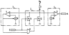
- the figure shows a basic circuit diagram of the circuit arrangement according to the invention.
- the circuit arrangement shown in the figure can be used as a driver stage for engine controls in motor vehicles will.
- a load 1 for example the coil of an electromagnetically controlled injection valve, is switched on or off by a control device (not shown) via the circuit arrangement with its input E, the circuit arrangement being used as a low-side driver.
- the load 1 is connected on the one hand to the supply voltage U B and on the other hand to the circuit arrangement, hereinafter referred to as the driver stage.
- the driver stage has a measuring resistor 2, which is implemented by the drain-source paths of two field-effect transistors T1 and T2 arranged in parallel.
- the total resistance of the parallel connection of the drain-source resistances of the transistors T1 and T2 results as the measuring resistor.
- Load 1 is switched on or off by a control unit via input E of the circuit arrangement, i.e. the gate connections of the transistors T1 and T2 are controlled by the control device.
- the source connections of the transistors T1 and T2 are each connected to ground and the drain connections are connected to the load 1.
- the voltage drop across the transistors T1 and T2 as a result of the load current flowing through the transistors is detected by a switching device 3 and a diagnostic device 4.
- the switching device 3 has a first comparator 5 and a first reference voltage source 6.
- the voltage that is present between the measuring resistor 2 and the load 1 (hereinafter referred to as measuring voltage) is compared with a first reference voltage (threshold value S1) generated by the reference voltage source 6.
- the output signal of the comparator 5 controls both the reference voltage source 6 and thus sets the threshold value S1 and an AND gate 8, which in turn switches transistor T2 on or off.
- the diagnostic device 4 has a second comparator 9 and a second reference voltage source 10. The measuring voltage is compared with a second reference voltage (threshold value S2) generated by the reference voltage source 10. If the line to load 1 is interrupted (indicated by a cross in the figure), a diagnostic signal is output at output A of the circuit arrangement.
- the circuit arrangement for detecting a line break works on the principle of a current measurement with a shunt.
- That voltage which is established across the measuring resistor 2 as a result of the current flow through the load 1 is detected and compared with the threshold values S1, S2. This voltage is referred to below as the measuring voltage.
- the measuring resistor 2 is divided into several resistance ranges, i.e. depending on the load current, the resistance value is changed so that there is a sufficiently large voltage drop both with a small and with a large load current across the measuring resistor.
- two different resistance values of the measuring resistor 2 can be set.
- the measuring resistor 2 is designed such that its resistance value is much larger with a small load current than with a large load current.
- the measuring voltage that is established is compared with the two threshold values S1 and S2, where: U B >S1>S2> 0 V
- the change in the measuring resistor 2 is controlled by the switching device 3, specifically when the measuring voltage falls below the first threshold value S1, for example with a small load current which has produced a small voltage drop across the measuring resistor 2.
- the measuring resistor is switched from a small value to a large one by blocking the transistor T2.
- the measuring voltage remains greater than the threshold value S2.
- the measuring voltage increases again and would now be greater than the threshold S1 if the threshold S1 had not been increased with the change in resistance. Otherwise this would have resulted in an oscillation of the circuit arrangement.
- This property of the switching device 3 can also be referred to as hysteresis.
- the first threshold value S1 which is determined by the first reference voltage source 6, is increased.
- the measuring voltage is therefore approximately 0 V.
- the second threshold value S2 the is determined by the second reference voltage source 10 is dimensioned such that it is then safely above this measuring voltage, but is less than the measuring voltage which arises with a small load current. If the measuring voltage is less than the threshold value S2, a diagnostic signal is generated in the diagnostic device 4, which is sent via the output A to an evaluation unit, not shown.
- the measuring resistance value is determined by the drain-source resistance of the transistors T1 and T2. It is particularly advantageous to use the drain-source resistance values trained very differently so that the circuit arrangement can be used in applications with a large load current range.
- the first transistor T1 has a drain-source resistance value in the conductive state of approximately 3 ⁇ and the second transistor T2 of approximately 0.3 ⁇ .
- the effective resistance value is determined by the parallel connection of transistors T1 and T2, i.e. it is approximately 0.27 ⁇ , and in the case of small load currents only by transistor T1 with approximately 3 ⁇ , since transistor T2 is blocked and then very has large drain-source resistance.
- both transistors T1 and T2 are blocked.
- both transistors T1 and T2 are initially conductive and the load current is distributed among them according to their drain-source resistance.
- the measuring voltage becomes smaller than the threshold value S1. Consequently, the transistor T2 is blocked via the output of the comparator 5 and the AND gate 8, while the transistor T1 continues to conduct.
- the circuit arrangement can be designed as an integrated circuit (IC).
- IC integrated circuit
- the different drain-source resistance values can be realized, for example, by transistor areas of different sizes.
- transistors T1 and T2 D-MOSFET transistors are particularly advantageous as transistors T1 and T2 D-MOSFET transistors to use. More than two transistors can also be arranged in parallel. This then corresponds to a measuring resistor 2 with several resistance stages which can be switched on as a function of the load current.
- the switching device together with the AND gate is replaced by a control device.
- the measuring resistor is not switched in stages, but continuously controlled.
- the measuring device regulates the measuring voltage to a constant value via the voltage at the gate connections of the transistors T1 and T2.
Abstract
Description
Die Erfindung betrifft eine Schaltungsanordnung zum Steuern einer Last und zum Erkennen einer Unterbrechung der Leitung zu der Last, vorzugsweise für den Einsatz in einem Kraftfahrzeug.The invention relates to a circuit arrangement for controlling a load and for detecting an interruption in the line to the load, preferably for use in a motor vehicle.
Bei einer bekannten Schaltungsanordnung zum Steuern einer Last (GB-A 2 034 550), wird eine Leitungsunterbrechung zwischen der Schaltungsanordnung und der Last bei eingeschalteter Last erkannt. Hierzu wird der Spannungsabfall über die Schaltungsanordnung erfaßt und ausgewertet. Wenn trotz eingeschalteter Last infolge eines Leitungsbruchs kein Laststrom fließt, so ist der Spannungsabfall über die Schaltungsanordnung annähernd null, d.h. die Spannung ist unter einen Grenzwert gefallen und ein Fehler wird erkannt.In a known circuit arrangement for controlling a load (GB-A 2 034 550), a line interruption between the circuit arrangement and the load is recognized when the load is switched on. For this purpose, the voltage drop is recorded and evaluated via the circuit arrangement. If, despite the load being switched on, no load current flows as a result of a line break, the voltage drop across the circuit arrangement is approximately zero, i.e. the voltage has dropped below a limit and an error is detected.
Allerdings ist die Spannung auch nahe null, wenn durch die Last nur ein sehr kleiner Laststrom fließt. Daher ist ein sicheres Erkennen einer Leitungsunterbrechung nicht möglich bei Schaltungsanordnungen, die sowohl bei kleinen als auch bei großen Lastströmen eingesetzt werden, d.h. bei Anwendungen mit einem großen Laststrombereich.However, the voltage is also close to zero if only a very small load current flows through the load. Therefore, it is not possible to reliably detect a line interruption in circuit arrangements which are used both with small and with large load currents, i.e. for applications with a large load current range.
Die Aufgabe der Erfindung ist es, eine Schaltungsanordnung zu schaffen, die eine Unterbrechung der Leitung zu der Last bei eingeschalteter Last und über einen großen Laststrombereich zuverlässig erkennt.The object of the invention is to provide a circuit arrangement which reliably detects an interruption in the line to the load when the load is switched on and over a large load current range.
Diese Aufgabe wird erfindungsgemäß durch eine Schaltungsanordnung mit den Merkmalen des Patentanspruchs 1 gelöst. Dabei wird ein Meßwiderstand in mehrere Bereiche aufgeteilt. Durch Ändern des Meßwiderstandes wird der Spannungsabfall über die Schaltungsanordnung und damit die Höhe der zu erfassenden Spannung an den Laststrom angepaßt. Deswegen ist die durch den Laststrom verursachte Verlustleistung gering.This object is achieved according to the invention by a circuit arrangement having the features of patent claim 1. A measuring resistor is divided into several areas. By changing the measuring resistance, the voltage drop adapted to the load current via the circuit arrangement and thus the level of the voltage to be detected. Therefore, the power loss caused by the load current is low.
Vorteilhafte Ausbildungen der Erfindung sind in den Unteransprüchen gekennzeichnet. Der Meßwiderstand kann durch Drain-Source-Widerstände von Feldeffekt-Transistoren realisiert werden. Eine Änderung des Meßwiderstandes erfolgt durch Ein- oder Ausschalten von einzelnen Transistoren, die parallel zueinander angeordnet sind.Advantageous developments of the invention are characterized in the subclaims. The measuring resistor can be implemented by drain-source resistors of field effect transistors. The measuring resistance is changed by switching individual transistors on or off, which are arranged in parallel with one another.
Besonders vorteilhaft ist es, wenn die Drain-Source-Widerstände mit stark unterschiedlichen Widerstandswerten realisiert sind, damit sich die zu erfassende Spannung besser an den jeweiligen Laststrom anpaßt. Der Spannungsabfall über die Schaltungsanordnung ist somit gering und begrenzt nicht die für die Last verfügbare Spannung.It is particularly advantageous if the drain-source resistors are implemented with very different resistance values, so that the voltage to be detected adapts better to the respective load current. The voltage drop across the circuit arrangement is thus small and does not limit the voltage available for the load.
Damit beim Ändern des Meßwiderstandes durch Umschalten des Widerstandswertes keine Oszillation entsteht, ist eine Umschalteinrichtung vorteilhafterweise mit einer Hysterese versehen.In order that no oscillation occurs when the measuring resistor is changed by switching the resistance value, a switching device is advantageously provided with a hysteresis.
Die Transistoren können mit der Umschalteinrichtung thermisch gekoppelt werden, um Temperatureinflüsse infolge des Laststromflusses durch die Transistoren zu kompensieren. Hierzu ist es günstig, wenn die Schaltungsanordnung als integrierter Schaltkreis ausgebildet ist.The transistors can be thermally coupled to the switching device in order to compensate for temperature influences due to the load current flow through the transistors. For this purpose, it is advantageous if the circuit arrangement is designed as an integrated circuit.
Ein Ausführungsbeispiel der Erfindung ist in der Zeichnung dargestellt und wird im folgenden näher erläutert.An embodiment of the invention is shown in the drawing and is explained in more detail below.
Die Figur zeigt ein prinzipielles Schaltbild der erfindungsgemäßen Schaltungsanordnung.The figure shows a basic circuit diagram of the circuit arrangement according to the invention.
Die in der Figur dargestellte Schaltungsanordnung kann als Treiberstufe für Motorsteuerungen bei Kraftfahrzeugen eingesetzt werden. Dabei wird eine Last 1, z.B. die Spule eines elektromagnetisch gesteuerten Einspritzventils, durch ein nicht dargestelltes Steuergerät über die Schaltungsanordnung mit ihrem Eingang E ein- oder ausgeschaltet, wobei die Schaltungsanordnung als Low-Side-Treiber eingesetzt wird. Dies bedeutet, daß die Last 1 einerseits an die Versorgungsspannung UB und andererseits an der Schaltungsanordnung, im folgenden als Treiberstufe bezeichnet, angeschlossen ist.The circuit arrangement shown in the figure can be used as a driver stage for engine controls in motor vehicles will. A load 1, for example the coil of an electromagnetically controlled injection valve, is switched on or off by a control device (not shown) via the circuit arrangement with its input E, the circuit arrangement being used as a low-side driver. This means that the load 1 is connected on the one hand to the supply voltage U B and on the other hand to the circuit arrangement, hereinafter referred to as the driver stage.
Die Treiberstufe weist einen Meßwiderstand 2 auf, der durch die Drain-Source-Strecken von zwei parallel angeordneten Feldeffekt-Transistoren T1 und T2 realisiert ist. Als Meßwiderstand ergibt sich der Gesamtwiderstand der Parallelschaltung der Drain-Source-Widerstände der Transistoren T1 und T2.The driver stage has a measuring resistor 2, which is implemented by the drain-source paths of two field-effect transistors T1 and T2 arranged in parallel. The total resistance of the parallel connection of the drain-source resistances of the transistors T1 and T2 results as the measuring resistor.
Die Last 1 wird durch ein Steuergerät über den Eingang E der Schaltungsanordnung ein- oder ausgeschaltet, d.h. die Gateanschlüsse der Transistoren T1 und T2 werden durch das Steuergerät gesteuert. Die Sourceanschlüsse der Transistoren T1 und T2 liegen jeweils auf Masse und die Drainanschlüsse sind mit der Last 1 verbunden.Load 1 is switched on or off by a control unit via input E of the circuit arrangement, i.e. the gate connections of the transistors T1 and T2 are controlled by the control device. The source connections of the transistors T1 and T2 are each connected to ground and the drain connections are connected to the load 1.
Der Spannungsabfall über die Transistoren T1 und T2 infolge des Laststromflusses durch die Transistoren wird durch eine Umschalteinrichtung 3 und eine Diagnoseeinrichtung 4 erfaßt. Die Umschalteinrichtung 3 weist einen ersten Komparator 5 und eine erste Referenzspannungsquelle 6 auf. Die Spannung, die zwischen dem Meßwiderstand 2 und der Last 1 anliegt (im folgenden als Meßspannung bezeichnet), wird mit einer von der Referenzspannungsquelle 6 erzeugten ersten Referenzspannung (Schwellwert S1) verglichen. Das Ausgangssignal des Komparators 5 steuert sowohl die Referenzspannungsquelle 6 und stellt somit den Schwellwert S1 ein als auch ein UND-Gatter 8, das wiederum den Transistor T2 ein- oder ausschaltet.The voltage drop across the transistors T1 and T2 as a result of the load current flowing through the transistors is detected by a switching device 3 and a
Die Diagnoseeinrichtung 4 weist einen zweiten Komparator 9 und eine zweite Referenzspannungsquelle 10 auf. Die Meßspannung wird mit einer von der Referenzspannungsquelle 10 erzeugten zweiten Referenzspannung (Schwellwert S2) verglichen. Bei einer Unterbrechung der Leitung zu der Last 1 (in der Figur durch ein Kreuz gekennzeichnet) wird am Ausgang A der Schaltungsanordnung ein Diagnosesignal ausgegeben.The
Das Steuern von Spannungsquellen ist von der Elektronik her hinreichend bekannt (z.B. Tietze, Schenk "Halbleiter-Schaltungstechnik", gesteuerte Quellen mit Stromspiegel) und wird daher nicht näher beschrieben.The control of voltage sources is well known from electronics (e.g. Tietze, Schenk "semiconductor circuit technology", controlled sources with current mirrors) and is therefore not described in detail.
Die Schaltungsanordnung zum Erkennen einer Leitungsunterbrechung funktioniert nach dem Prinzip einer Strommessung mit einem Shunt. Bei eingeschalteter Treiberstufe wird diejenige Spannung, die sich über den Meßwiderstand 2 infolge des Stromflusses durch die Last 1 einstellt, erfaßt und mit den Schwellwerten S1, S2 verglichen. Diese Spannung wird im folgenden als Meßspannung bezeichnet.The circuit arrangement for detecting a line break works on the principle of a current measurement with a shunt. When the driver stage is switched on, that voltage which is established across the measuring resistor 2 as a result of the current flow through the load 1 is detected and compared with the threshold values S1, S2. This voltage is referred to below as the measuring voltage.
Um eine Leitungsunterbrechung über einen großen Laststrombereich sicher erkennen zu können, wird der Meßwiderstand 2 in mehrere Widerstandsbereiche aufgeteilt, d.h. in Abhängigkeit von dem Laststrom wird der Widerstandswert so geändert, daß sich ein genügend großer Spannungsabfall sowohl bei einem kleinen als auch bei einem großen Laststrom über den Meßwiderstand ergibt.In order to be able to reliably detect a line interruption over a large load current range, the measuring resistor 2 is divided into several resistance ranges, i.e. depending on the load current, the resistance value is changed so that there is a sufficiently large voltage drop both with a small and with a large load current across the measuring resistor.
Bei dem vorliegenden Ausführungsbeispiel können zwei verschiedene Widerstandswerte des Meßwiderstands 2 eingestellt werden. Hierzu ist der Meßwiderstand 2 so ausgebildet, daß sein Widerstandswert bei einem kleinen Laststrom viel größer ist, als bei einem großen Laststrom. Die sich einstellende Meßspannung wird mit den zwei Schwellwerten S1 und S2 verglichen, wobei gilt:
![]()
Die Änderung des Meßwiderstands 2 wird durch die Umschalteinrichtung 3 gesteuert, und zwar dann, wenn die Meßspannung den ersten Schwellwert S1 unterschreitet, z.B. bei einem kleinen Laststrom, der einen kleinen Spannungsabfall über den Meßwiderstand 2 erzeugt hat. Der Meßwiderstand wird von einem kleinen Wert auf einen großen umgeschaltet, indem der Transistor T2 gesperrt wird. Die Meßspannung bleibt größer als der Schwellwert S2.In the present exemplary embodiment, two different resistance values of the measuring resistor 2 can be set. For this purpose, the measuring resistor 2 is designed such that its resistance value is much larger with a small load current than with a large load current. The measuring voltage that is established is compared with the two threshold values S1 and S2, where:
![]()
The change in the measuring resistor 2 is controlled by the switching device 3, specifically when the measuring voltage falls below the first threshold value S1, for example with a small load current which has produced a small voltage drop across the measuring resistor 2. The measuring resistor is switched from a small value to a large one by blocking the transistor T2. The measuring voltage remains greater than the threshold value S2.
Als Nebeneffekt erhöht sich die Meßspannung wieder und wäre nun größer als der Schwellwert S1, wenn mit der Widerstandsänderung der Schwellwert S1 nicht erhöht worden wäre. Dies hätte sonst eine Oszillation der Schaltungsanordnung zur Folge hat. Diese Eigenschaft der Umschalteinrichtung 3 kann auch als Hysterese bezeichnet werden. Hierfür wird der erste Schwellwert S1, der durch die erste Referenzspannungsquelle 6 bestimmt wird, erhöht.As a side effect, the measuring voltage increases again and would now be greater than the threshold S1 if the threshold S1 had not been increased with the change in resistance. Otherwise this would have resulted in an oscillation of the circuit arrangement. This property of the switching device 3 can also be referred to as hysteresis. For this purpose, the first threshold value S1, which is determined by the first reference voltage source 6, is increased.
Bei einer nicht beabsichtigten Unterbrechung der Leitung zu der Last 1 fließt nur noch ein sehr geringer Reststrom, der nur durch Eingangsströme der Komparatoren 6 und 9 bedingt ist, durch den Meßwiderstand 2. Die Meßspannung ist daher annähernd 0 V. Der zweite Schwellwert S2, der durch die zweite Referenzspannungsquelle 10 bestimmt wird, ist so bemessen, daß er dann sicher über dieser Meßspannung liegt, aber kleiner ist als die Meßspannung, die sich bei einem kleinen Laststrom einstellt. Wenn die Meßspannung kleiner als der Schwellwert S2 ist, wird ein Diagnosesignal in der Diagnoseeinrichtung 4 erzeugt, das über den Ausgang A zu einer nicht dargestellten Auswerteeinheit gesendet wird.In the event of an unintentional interruption of the line to the load 1, only a very small residual current, which is only caused by input currents from the
Wenn der Meßwiderstand 2 durch Feldeffekt-Transistoren T1 und T2 realisiert ist, wird der Meßwiderstandswert durch den Drain-Source-Widerstand der Transistoren T1 und T2 bestimmt. Besonders vorteilhaft ist es, die Drain-Source-Widerstandswerte stark unterschiedlich auszubilden, damit die Schaltungsanordnung bei Anwendungen mit einem großen Laststrombereich eingesetzt werden kann.If the measuring resistor 2 is realized by field effect transistors T1 and T2, the measuring resistance value is determined by the drain-source resistance of the transistors T1 and T2. It is particularly advantageous to use the drain-source resistance values trained very differently so that the circuit arrangement can be used in applications with a large load current range.
Der erste Transistor T1 hat einen Drain-Source-Widerstandswert im leitenden Zustand von etwa 3 Ω und der zweite Transistor T2 von etwa 0,3 Ω. Bei großen Lastströmen wird der wirksame Widerstandswert durch die Parallelschaltung der Transistoren T1 und T2 bestimmt, er ist also etwa 0,27 Ω, und bei kleinen Lastströmen nur durch den Transistor T1 mit etwa 3 Ω, da der Transistor T2 gesperrt ist und dann einen sehr großen Drain-Source-Widerstand hat.The first transistor T1 has a drain-source resistance value in the conductive state of approximately 3 Ω and the second transistor T2 of approximately 0.3 Ω. In the case of large load currents, the effective resistance value is determined by the parallel connection of transistors T1 and T2, i.e. it is approximately 0.27 Ω, and in the case of small load currents only by transistor T1 with approximately 3 Ω, since transistor T2 is blocked and then very has large drain-source resistance.
Im Ruhezustand, d.h. wenn kein Laststrom fließen soll, sind beide Transistoren T1 und T2 gesperrt. Wenn ein Laststrom fließ, sind beide Transistoren T1 und T2 zunächst leitend und der Laststrom verteilt sich auf sie entsprechend ihrem Drain-Source-Widerstand. Wenn der Laststrom jedoch eine gewisse Größe unterschreitet, wird die Meßspannung kleiner als der Schwellwert S1. Folglich wird über den Ausgang des Komparators 5 und das UND-Gatter 8 der Transistor T2 gesperrt, während der Transistor T1 weiterhin leitet.At rest, i.e. if no load current is to flow, both transistors T1 and T2 are blocked. When a load current flows, both transistors T1 and T2 are initially conductive and the load current is distributed among them according to their drain-source resistance. However, if the load current falls below a certain size, the measuring voltage becomes smaller than the threshold value S1. Consequently, the transistor T2 is blocked via the output of the comparator 5 and the AND gate 8, while the transistor T1 continues to conduct.
Die Schaltungsanordnung kann als integrierter Schaltkreis (IC) ausgebildet sein. In einem solchen IC können die unterschiedlichen Drain-Source-Widerstandswerte beispielsweise durch unterschiedlich große Transistorflächen realisiert werden.The circuit arrangement can be designed as an integrated circuit (IC). In such an IC, the different drain-source resistance values can be realized, for example, by transistor areas of different sizes.
In einem IC ist es auch vorteilhaft, eine durch Temperaturänderung der Transistoren T1 und T2 verursachte Drift der Meßspannung dadurch zu kompensieren, daß die erste Referenzspannungsquelle 6 in die Nähe der Transistoren T1 und T2 plaziert wird, damit der Schwellwert auch eine Temperaturdrift in gleicher Richtung erfährt.In an IC, it is also advantageous to compensate for a drift in the measurement voltage caused by the temperature change in the transistors T1 and T2 by placing the first reference voltage source 6 in the vicinity of the transistors T1 and T2 so that the threshold value also experiences a temperature drift in the same direction .
Besonders vorteilhaft ist es, als Transistoren T1 und T2 D-MOSFET-Transistoren einzusetzen. Es können auch mehr als zwei Transistoren parallel angeordnet werden. Dies entspricht dann einem Meßwiderstand 2 mit mehreren Widerstandsstufen, die in Abhängigkeit von dem Laststrom eingeschaltet werden können.It is particularly advantageous as transistors T1 and T2 D-MOSFET transistors to use. More than two transistors can also be arranged in parallel. This then corresponds to a measuring resistor 2 with several resistance stages which can be switched on as a function of the load current.
Bei einem weiteren, nicht dargestellten Ausführungsbeispiel (Elemente gleicher Funktion tragen dieselben Bezeichnungen wie im ersten Ausführungsbeispiel) ist die Umschalteinrichtung zusammen mit dem UND-Gatter durch eine Regeleinrichtung ersetzt. Dabei wird der Meßwiderstand nicht stufenweise geschaltet, sondern kontinuierlich geregelt. Durch die Regeleinrichtung wird über die Spannung an den Gateanschlüssen der Transistoren T1 und T2 die Meßspannung auf einen konstanten Wert geregelt.In a further exemplary embodiment, not shown (elements with the same function have the same designations as in the first exemplary embodiment), the switching device together with the AND gate is replaced by a control device. The measuring resistor is not switched in stages, but continuously controlled. The measuring device regulates the measuring voltage to a constant value via the voltage at the gate connections of the transistors T1 and T2.
Claims (7)
dadurch gekennzeichnet, daß
sie einen Meßwiderstand (2), der in Reihe zu der Last (1) angeordnet ist und dessen Widerstandswert in Abhängigkeit von dem Laststrom durch eine Umschalteinrichtung (3) geändert wird, sowie eine Diagnoseeinrichtung (4) aufweist, die ein Diagnosesignal erzeugt, wenn der durch den Laststrom hervorgerufenen Spannungsabfall über den Meßwiderstand (2) einen Schwellwert unterschreitet.Circuit arrangement for controlling a load (1) and for detecting an interruption in the line to the load,
characterized in that
it has a measuring resistor (2) which is arranged in series with the load (1) and whose resistance value is changed as a function of the load current by a switching device (3), and has a diagnostic device (4) which generates a diagnostic signal when the voltage drop across the measuring resistor (2) caused by the load current falls below a threshold value.
Priority Applications (4)
| Application Number | Priority Date | Filing Date | Title |
|---|---|---|---|
| DE59201675T DE59201675D1 (en) | 1992-08-07 | 1992-08-07 | Circuit arrangement for controlling a load and for detecting a line break. |
| EP92113493A EP0581993B1 (en) | 1992-08-07 | 1992-08-07 | Circuit arrangement for the control of a load and the detection of line interruption |
| JP21357993A JP3383688B2 (en) | 1992-08-07 | 1993-08-06 | Circuit device for controlling load and identifying disconnection state |
| US08/104,327 US5570259A (en) | 1992-08-07 | 1993-08-09 | Circuit arrangement for controlling a load and for recognizing a line interruption |
Applications Claiming Priority (1)
| Application Number | Priority Date | Filing Date | Title |
|---|---|---|---|
| EP92113493A EP0581993B1 (en) | 1992-08-07 | 1992-08-07 | Circuit arrangement for the control of a load and the detection of line interruption |
Publications (2)
| Publication Number | Publication Date |
|---|---|
| EP0581993A1 true EP0581993A1 (en) | 1994-02-09 |
| EP0581993B1 EP0581993B1 (en) | 1995-03-15 |
Family
ID=8209889
Family Applications (1)
| Application Number | Title | Priority Date | Filing Date |
|---|---|---|---|
| EP92113493A Expired - Lifetime EP0581993B1 (en) | 1992-08-07 | 1992-08-07 | Circuit arrangement for the control of a load and the detection of line interruption |
Country Status (4)
| Country | Link |
|---|---|
| US (1) | US5570259A (en) |
| EP (1) | EP0581993B1 (en) |
| JP (1) | JP3383688B2 (en) |
| DE (1) | DE59201675D1 (en) |
Cited By (5)
| Publication number | Priority date | Publication date | Assignee | Title |
|---|---|---|---|---|
| FR2743635A1 (en) * | 1996-01-11 | 1997-07-18 | Sgs Thomson Microelectronics | CURRENT MEASUREMENT CIRCUIT |
| EP0987724A2 (en) * | 1998-09-17 | 2000-03-22 | Atlas Copco Electric Tools GmbH | Hand-held power tool |
| WO2008071722A1 (en) * | 2006-12-13 | 2008-06-19 | Siemens Aktiengesellschaft | Measuring apparatus for measuring an electrical current |
| WO2012001157A1 (en) * | 2010-07-01 | 2012-01-05 | Continental Teves Ag & Co. Ohg | Current sensor |
| WO2014095226A1 (en) * | 2012-12-20 | 2014-06-26 | Continental Teves Ag & Co. Ohg | Method for setting up a current sensor |
Families Citing this family (15)
| Publication number | Priority date | Publication date | Assignee | Title |
|---|---|---|---|---|
| DE4234402A1 (en) * | 1992-10-07 | 1994-04-14 | Siemens Ag | Arrangement for transmitting binary signals over a signal line |
| DE69611826T2 (en) * | 1996-09-17 | 2001-06-07 | St Microelectronics Srl | Circuit for diagnosing the condition of an electrical load |
| DE19741780B4 (en) * | 1997-09-22 | 2005-07-28 | Siemens Ag | Method for detecting line breaks in an inductive sensor |
| US6194951B1 (en) * | 1998-09-15 | 2001-02-27 | Siemens Aktiengesellschaft | Method and device for diving an integrated power output stage |
| DE10246107B4 (en) * | 2002-10-02 | 2015-11-26 | Continental Automotive Gmbh | Method and circuit arrangement for fault monitoring of at least one electrical load |
| JP2004226115A (en) * | 2003-01-20 | 2004-08-12 | Elpida Memory Inc | Semiconductor device and its testing method |
| DE10335083B3 (en) * | 2003-07-31 | 2004-12-16 | Infineon Technologies Ag | Load diagnosis circuit arrangement, for semiconductor switch, has circuit for evaluating currents flowing to first and second connection terminals and providing load state signal depending on these currents |
| EP1957992B1 (en) | 2005-12-06 | 2011-05-25 | Harman International Industries, Incorporated | Diagnostic system for power converter |
| CN103477234A (en) * | 2011-03-29 | 2013-12-25 | 大陆-特韦斯贸易合伙股份公司及两合公司 | Current sensor |
| EP2760093B1 (en) * | 2013-01-29 | 2017-04-12 | Delphi Technologies, Inc. | Power switch fault detection system |
| US9568504B2 (en) * | 2013-03-15 | 2017-02-14 | Milwaukee Electric Tool Corporation | Digital multi-meter |
| JP6628537B2 (en) * | 2015-10-02 | 2020-01-08 | 日本信号株式会社 | Communication abnormality detection system and communication abnormality detection method |
| US10527661B2 (en) * | 2018-02-07 | 2020-01-07 | Rockwell Automation Technologies, Inc. | Calculating a load resistance |
| US10901035B2 (en) * | 2019-02-01 | 2021-01-26 | Intel Corporation | Techniques in ensuring functional safety (fusa) systems |
| CN110426549A (en) * | 2019-08-14 | 2019-11-08 | 上海爻火微电子有限公司 | The current detection circuit and electronic equipment of power channel |
Citations (2)
| Publication number | Priority date | Publication date | Assignee | Title |
|---|---|---|---|---|
| DE3312304A1 (en) * | 1983-04-06 | 1984-10-11 | Neumann Elektronik GmbH, 4330 Mülheim | Device for automatically switching the output level of a power amplifier |
| DE3907880A1 (en) * | 1989-03-10 | 1990-09-13 | Siemens Ag | Circuit arrangement for outputting binary signals |
Family Cites Families (3)
| Publication number | Priority date | Publication date | Assignee | Title |
|---|---|---|---|---|
| GB2034550B (en) * | 1978-10-21 | 1983-03-02 | Ward Goldstone Ltd | Indicating faults in soldid state switching circuits |
| US4375073A (en) * | 1980-06-16 | 1983-02-22 | Reliance Electric Company | Dual-monitoring protection circuit for switching transistor |
| US5057719A (en) * | 1990-06-27 | 1991-10-15 | Sverdrup Technology, Inc. | Passively forced current sharing among transistors |
-
1992
- 1992-08-07 EP EP92113493A patent/EP0581993B1/en not_active Expired - Lifetime
- 1992-08-07 DE DE59201675T patent/DE59201675D1/en not_active Expired - Lifetime
-
1993
- 1993-08-06 JP JP21357993A patent/JP3383688B2/en not_active Expired - Fee Related
- 1993-08-09 US US08/104,327 patent/US5570259A/en not_active Expired - Lifetime
Patent Citations (2)
| Publication number | Priority date | Publication date | Assignee | Title |
|---|---|---|---|---|
| DE3312304A1 (en) * | 1983-04-06 | 1984-10-11 | Neumann Elektronik GmbH, 4330 Mülheim | Device for automatically switching the output level of a power amplifier |
| DE3907880A1 (en) * | 1989-03-10 | 1990-09-13 | Siemens Ag | Circuit arrangement for outputting binary signals |
Cited By (9)
| Publication number | Priority date | Publication date | Assignee | Title |
|---|---|---|---|---|
| FR2743635A1 (en) * | 1996-01-11 | 1997-07-18 | Sgs Thomson Microelectronics | CURRENT MEASUREMENT CIRCUIT |
| EP0789246A1 (en) * | 1996-01-11 | 1997-08-13 | STMicroelectronics S.A. | Current measuring circuit |
| US5845275A (en) * | 1996-01-11 | 1998-12-01 | Sgs-Thomson Microelectronics S.A. | Current measurement circuit |
| EP0987724A2 (en) * | 1998-09-17 | 2000-03-22 | Atlas Copco Electric Tools GmbH | Hand-held power tool |
| EP0987724A3 (en) * | 1998-09-17 | 2000-11-22 | Atlas Copco Electric Tools GmbH | Hand-held power tool |
| WO2008071722A1 (en) * | 2006-12-13 | 2008-06-19 | Siemens Aktiengesellschaft | Measuring apparatus for measuring an electrical current |
| WO2012001157A1 (en) * | 2010-07-01 | 2012-01-05 | Continental Teves Ag & Co. Ohg | Current sensor |
| KR101921765B1 (en) | 2010-07-01 | 2019-02-13 | 콘티넨탈 테베스 아게 운트 코. 오하게 | Current sensor |
| WO2014095226A1 (en) * | 2012-12-20 | 2014-06-26 | Continental Teves Ag & Co. Ohg | Method for setting up a current sensor |
Also Published As
| Publication number | Publication date |
|---|---|
| EP0581993B1 (en) | 1995-03-15 |
| DE59201675D1 (en) | 1995-04-20 |
| JPH06205531A (en) | 1994-07-22 |
| JP3383688B2 (en) | 2003-03-04 |
| US5570259A (en) | 1996-10-29 |
Similar Documents
| Publication | Publication Date | Title |
|---|---|---|
| EP0581993B1 (en) | Circuit arrangement for the control of a load and the detection of line interruption | |
| DE4015625C2 (en) | Transistor with current detection function, the current detection resistor is temperature compensated | |
| DE4207568C2 (en) | Overcurrent detector circuit for a power semiconductor device | |
| DE19544863C2 (en) | Sensor device | |
| DE102006054354A1 (en) | Protective circuit for electrical appliance, has short circuit short circuiting output or input clamps during exceedance of threshold value, where control signal regulates limit has same origin as that of circuit that controls short circuit | |
| DE102005003643B4 (en) | Circuit device with a current limiter of an output transistor | |
| DE3338124C2 (en) | ||
| DE2610177C2 (en) | Sensor amplifier with at least two operating states | |
| DE3931921A1 (en) | POWER CONTROL UNIT | |
| DE69614659T2 (en) | Circuit with overcurrent protection for power transistors | |
| DE4316275A1 (en) | MOS power switching circuit IC with short circuit protection - has current limiter between source of MOS power transistor and base of bipolar transistor | |
| DE3132257A1 (en) | PROTECTIVE CIRCUIT FOR A FIELD EFFECT TRANSISTOR IN A LOAD CIRCUIT | |
| DE3233536A1 (en) | DEVICE FOR THE CLOCKED REGULATION OF A COIL FLOWING THROUGH | |
| DE69838973T2 (en) | Low power monitoring by "low-side" driven DMOS by modulating its internal resistance | |
| EP0698794A1 (en) | Under voltage detection circuit | |
| DE4335683A1 (en) | Constant current source | |
| EP0098460B1 (en) | Control device for an electrical actuator | |
| DE4020187C2 (en) | ||
| DE19855870B4 (en) | Flow sensor of the heat sensitive type | |
| EP0410188B1 (en) | Circuit arrangement for protecting a clocked semi-conductor switch | |
| DE2148437C3 (en) | Circuit arrangement for improving the short-circuit strength of circuits of the slow, fail-safe logic type | |
| DE4428115A1 (en) | Control unit with a circuit arrangement for protecting the control unit when the control unit mass is interrupted | |
| DE3013474A1 (en) | SENSOR SYSTEM | |
| DE4223274A1 (en) | DRIVER CIRCUIT FOR INDUCTIVE LOADS | |
| EP0575587B1 (en) | Undervoltage detection circuit |
Legal Events
| Date | Code | Title | Description |
|---|---|---|---|
| PUAI | Public reference made under article 153(3) epc to a published international application that has entered the european phase |
Free format text: ORIGINAL CODE: 0009012 |
|
| 17P | Request for examination filed |
Effective date: 19920824 |
|
| AK | Designated contracting states |
Kind code of ref document: A1 Designated state(s): AT BE CH DE DK ES FR GB GR IE IT LI LU MC NL PT SE |
|
| RBV | Designated contracting states (corrected) |
Designated state(s): DE FR GB IT |
|
| 17Q | First examination report despatched |
Effective date: 19940826 |
|
| GRAA | (expected) grant |
Free format text: ORIGINAL CODE: 0009210 |
|
| AK | Designated contracting states |
Kind code of ref document: B1 Designated state(s): DE FR GB IT |
|
| REF | Corresponds to: |
Ref document number: 59201675 Country of ref document: DE Date of ref document: 19950420 |
|
| ITF | It: translation for a ep patent filed |
Owner name: STUDIO JAUMANN |
|
| ET | Fr: translation filed | ||
| GBT | Gb: translation of ep patent filed (gb section 77(6)(a)/1977) |
Effective date: 19950605 |
|
| PLBE | No opposition filed within time limit |
Free format text: ORIGINAL CODE: 0009261 |
|
| STAA | Information on the status of an ep patent application or granted ep patent |
Free format text: STATUS: NO OPPOSITION FILED WITHIN TIME LIMIT |
|
| 26N | No opposition filed | ||
| REG | Reference to a national code |
Ref country code: GB Ref legal event code: IF02 |
|
| PGFP | Annual fee paid to national office [announced via postgrant information from national office to epo] |
Ref country code: DE Payment date: 20100831 Year of fee payment: 19 |
|
| REG | Reference to a national code |
Ref country code: GB Ref legal event code: 732E Free format text: REGISTERED BETWEEN 20110519 AND 20110525 |
|
| PGFP | Annual fee paid to national office [announced via postgrant information from national office to epo] |
Ref country code: FR Payment date: 20110901 Year of fee payment: 20 Ref country code: GB Payment date: 20110819 Year of fee payment: 20 |
|
| REG | Reference to a national code |
Ref country code: FR Ref legal event code: TQ Owner name: HARRIS SEMICONDUCTOR GMBH, DE Effective date: 20111104 Ref country code: FR Ref legal event code: TQ Owner name: CONTINENTAL AUTOMOTIVE GMBH, DE Effective date: 20111104 |
|
| PGFP | Annual fee paid to national office [announced via postgrant information from national office to epo] |
Ref country code: IT Payment date: 20110824 Year of fee payment: 20 |
|
| REG | Reference to a national code |
Ref country code: DE Ref legal event code: R119 Ref document number: 59201675 Country of ref document: DE Effective date: 20120301 |
|
| REG | Reference to a national code |
Ref country code: GB Ref legal event code: PE20 Expiry date: 20120806 |
|
| PG25 | Lapsed in a contracting state [announced via postgrant information from national office to epo] |
Ref country code: GB Free format text: LAPSE BECAUSE OF EXPIRATION OF PROTECTION Effective date: 20120806 |
|
| PG25 | Lapsed in a contracting state [announced via postgrant information from national office to epo] |
Ref country code: DE Free format text: LAPSE BECAUSE OF NON-PAYMENT OF DUE FEES Effective date: 20120301 |